Rangkaian Speaker Aktif Buat HP +3,7 Volt1__LM4868
28
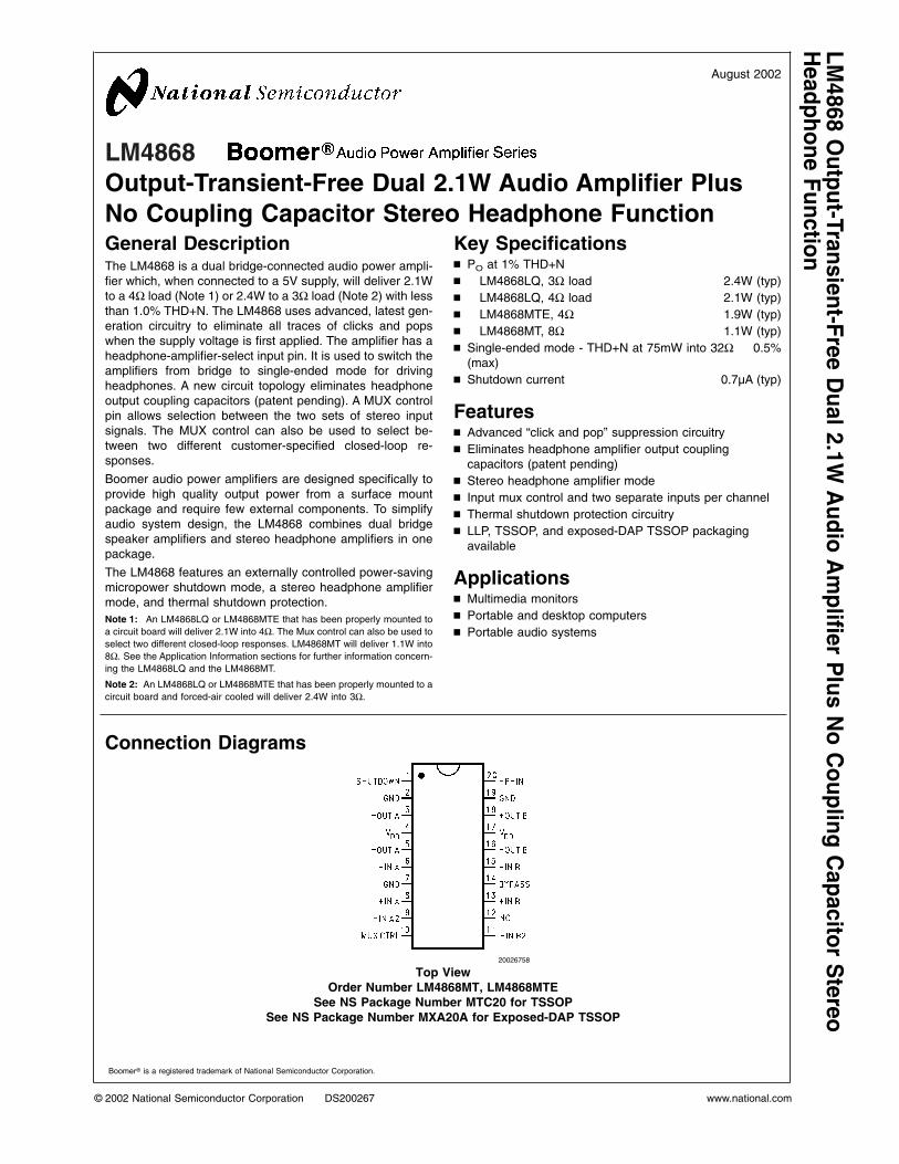
LM4868 Output-Transient-Free Dual 2.1W Audio Amplifier Plus No Coupling Capacitor Stereo Headphone Function General Description The LM4868 is a dual bridge-connected audio power ampli- fier which, when connected to a 5V supply, will deliver 2.1W to a 4Ω load (Note 1) or 2.4W to a 3Ω load (Note 2) with less than 1.0% THD+N. The LM4868 uses advanced, latest gen- eration circuitry to eliminate all traces of clicks and pops when the supply voltage is first applied. The amplifier has a headphone-amplifier-select input pin. It is used to switch the amplifiers from bridge to single-ended mode for driving headphones. A new circuit topology eliminates headphone output coupling capacitors (patent pending). A MUX control pin allows selection between the two sets of stereo input signals. The MUX control can also be used to select be- tween two different customer-specified closed-loop re- sponses. Boomer audio power amplifiers are designed specifically to provide high quality output power from a surface mount package and require few external components. To simplify audio system design, the LM4868 combines dual bridge speaker amplifiers and stereo headphone amplifiers in one package. The LM4868 features an externally controlled power-saving micropower shutdown mode, a stereo headphone amplifier mode, and thermal shutdown protection. Note 1: An LM4868LQ or LM4868MTE that has been properly mounted to a circuit board will deliver 2.1W into 4Ω. The Mux control can also be used to select two different closed-loop responses. LM4868MT will deliver 1.1W into 8Ω. See the Application Information sections for further information concern- ing the LM4868LQ and the LM4868MT. Note 2: An LM4868LQ or LM4868MTE that has been properly mounted to a circuit board and forced-air cooled will deliver 2.4W into 3Ω. Key Specifications n P O at 1% THD+N n LM4868LQ, 3Ω load 2.4W (typ) n LM4868LQ, 4Ω load 2.1W (typ) n LM4868MTE, 4Ω 1.9W (typ) n LM4868MT, 8Ω 1.1W (typ) n Single-ended mode - THD+N at 75mW into 32Ω 0.5% (max) n Shutdown current 0.7μA (typ) Features n Advanced “click and pop” suppression circuitry n Eliminates headphone amplifier output coupling capacitors (patent pending) n Stereo headphone amplifier mode n Input mux control and two separate inputs per channel n Thermal shutdown protection circuitry n LLP, TSSOP, and exposed-DAP TSSOP packaging available Applications n Multimedia monitors n Portable and desktop computers n Portable audio systems Connection Diagrams 20026758 Top View Order Number LM4868MT, LM4868MTE See NS Package Number MTC20 for TSSOP See NS Package Number MXA20A for Exposed-DAP TSSOP Boomer ® is a registered trademark of National Semiconductor Corporation. August 2002 LM4868 Output-Transient-Free Dual 2.1W Audio Amplifier Plus No Coupling Capacitor Stereo Headphone Function © 2002 National Semiconductor Corporation DS200267 www.national.com
-
Upload
dony-donkers -
Category
Documents
-
view
130 -
download
9
Transcript of Rangkaian Speaker Aktif Buat HP +3,7 Volt1__LM4868
LM4868Output-Transient-Free Dual 2.1W Audio Amplifier PlusNo Coupling Capacitor Stereo Headphone FunctionGeneral DescriptionThe LM4868 is a dual bridge-connected audio power ampli-fier which, when connected to a 5V supply, will deliver 2.1Wto a 4Ω load (Note 1) or 2.4W to a 3Ω load (Note 2) with lessthan 1.0% THD+N. The LM4868 uses advanced, latest gen-eration circuitry to eliminate all traces of clicks and popswhen the supply voltage is first applied. The amplifier has aheadphone-amplifier-select input pin. It is used to switch theamplifiers from bridge to single-ended mode for drivingheadphones. A new circuit topology eliminates headphoneoutput coupling capacitors (patent pending). A MUX controlpin allows selection between the two sets of stereo inputsignals. The MUX control can also be used to select be-tween two different customer-specified closed-loop re-sponses.
Boomer audio power amplifiers are designed specifically toprovide high quality output power from a surface mountpackage and require few external components. To simplifyaudio system design, the LM4868 combines dual bridgespeaker amplifiers and stereo headphone amplifiers in onepackage.
The LM4868 features an externally controlled power-savingmicropower shutdown mode, a stereo headphone amplifiermode, and thermal shutdown protection.Note 1: An LM4868LQ or LM4868MTE that has been properly mounted toa circuit board will deliver 2.1W into 4Ω. The Mux control can also be used toselect two different closed-loop responses. LM4868MT will deliver 1.1W into8Ω. See the Application Information sections for further information concern-ing the LM4868LQ and the LM4868MT.
Note 2: An LM4868LQ or LM4868MTE that has been properly mounted to acircuit board and forced-air cooled will deliver 2.4W into 3Ω.
Key Specificationsn PO at 1% THD+Nn LM4868LQ, 3Ω load 2.4W (typ)n LM4868LQ, 4Ω load 2.1W (typ)n LM4868MTE, 4Ω 1.9W (typ)n LM4868MT, 8Ω 1.1W (typ)n Single-ended mode - THD+N at 75mW into 32Ω 0.5%
(max)n Shutdown current 0.7µA (typ)
Featuresn Advanced “click and pop” suppression circuitryn Eliminates headphone amplifier output coupling
capacitors (patent pending)n Stereo headphone amplifier moden Input mux control and two separate inputs per channeln Thermal shutdown protection circuitryn LLP, TSSOP, and exposed-DAP TSSOP packaging
available
Applicationsn Multimedia monitorsn Portable and desktop computersn Portable audio systems
Connection Diagrams
20026758
Top ViewOrder Number LM4868MT, LM4868MTE
See NS Package Number MTC20 for TSSOPSee NS Package Number MXA20A for Exposed-DAP TSSOP
Boomer® is a registered trademark of National Semiconductor Corporation.
August 2002LM
4868O
utput-Transient-FreeD
ual2.1WA
udioA
mplifier
Plus
No
Coupling
Capacitor
Stereo
Headphone
Function
© 2002 National Semiconductor Corporation DS200267 www.national.com
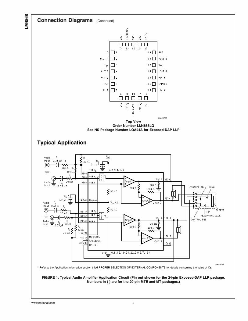
Connection Diagrams (Continued)
20026738
Top ViewOrder Number LM4868LQ
See NS Package Number LQA24A for Exposed-DAP LLP
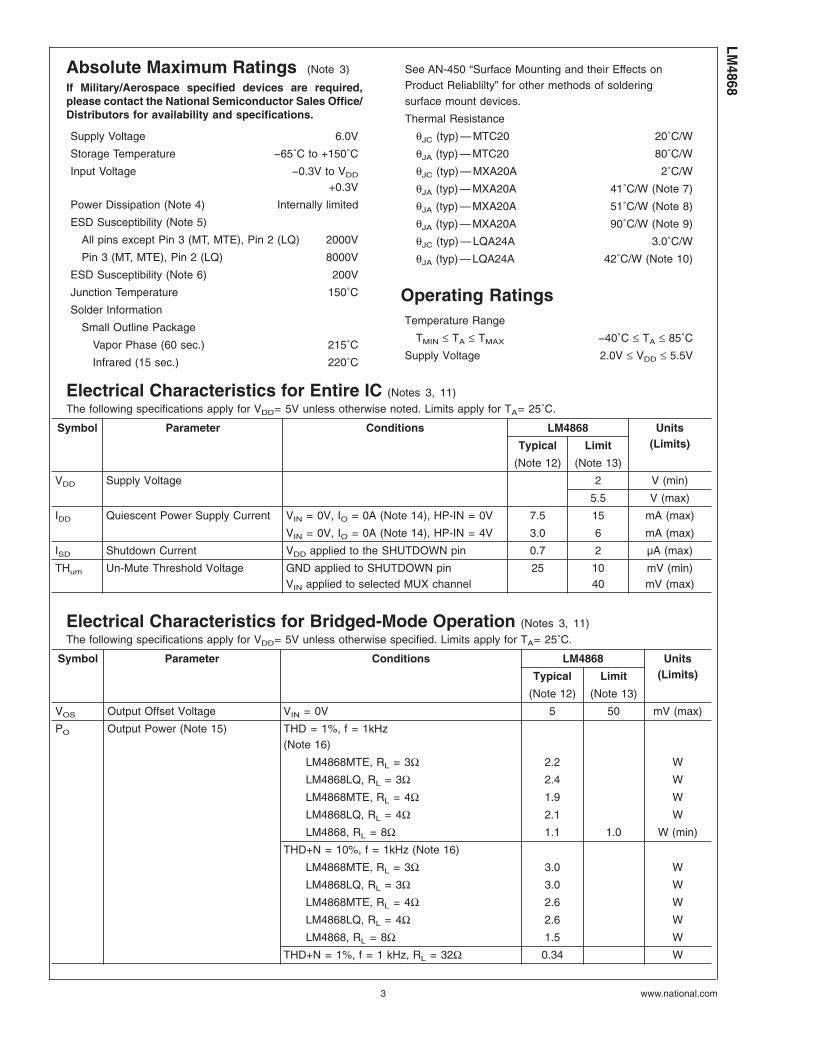
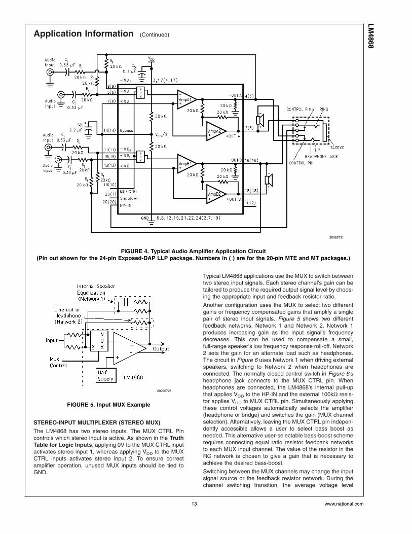
Typical Application
20026731
* Refer to the Application Information section titled PROPER SELECTION OF EXTERNAL COMPONENTS for details concerning the value of CB.
FIGURE 1. Typical Audio Amplifier Application Circuit (Pin out shown for the 24-pin Exposed-DAP LLP package.Numbers in ( ) are for the 20-pin MTE and MT packages.)
LM48
68
www.national.com 2
Absolute Maximum Ratings (Note 3)
If Military/Aerospace specified devices are required,please contact the National Semiconductor Sales Office/Distributors for availability and specifications.
Supply Voltage 6.0V
Storage Temperature −65˚C to +150˚C
Input Voltage −0.3V to VDD
+0.3V
Power Dissipation (Note 4) Internally limited
ESD Susceptibility (Note 5)
All pins except Pin 3 (MT, MTE), Pin 2 (LQ) 2000V
Pin 3 (MT, MTE), Pin 2 (LQ) 8000V
ESD Susceptibility (Note 6) 200V
Junction Temperature 150˚C
Solder Information
Small Outline Package
Vapor Phase (60 sec.) 215˚C
Infrared (15 sec.) 220˚C
See AN-450 “Surface Mounting and their Effects onProduct Reliablilty” for other methods of solderingsurface mount devices.
Thermal Resistance
θJC (typ) — MTC20 20˚C/W
θJA (typ) — MTC20 80˚C/W
θJC (typ) — MXA20A 2˚C/W
θJA (typ) — MXA20A 41˚C/W (Note 7)
θJA (typ) — MXA20A 51˚C/W (Note 8)
θJA (typ) — MXA20A 90˚C/W (Note 9)
θJC (typ) — LQA24A 3.0˚C/W
θJA (typ) — LQA24A 42˚C/W (Note 10)
Operating RatingsTemperature Range
TMIN ≤ TA ≤ TMAX −40˚C ≤ TA ≤ 85˚C
Supply Voltage 2.0V ≤ VDD ≤ 5.5V
Electrical Characteristics for Entire IC (Notes 3, 11)
The following specifications apply for VDD= 5V unless otherwise noted. Limits apply for TA= 25˚C.
Symbol Parameter Conditions LM4868 Units(Limits)Typical Limit
(Note 12) (Note 13)
VDD Supply Voltage 2 V (min)
5.5 V (max)
IDD Quiescent Power Supply Current VIN = 0V, IO = 0A (Note 14), HP-IN = 0V 7.5 15 mA (max)
VIN = 0V, IO = 0A (Note 14), HP-IN = 4V 3.0 6 mA (max)
ISD Shutdown Current VDD applied to the SHUTDOWN pin 0.7 2 µA (max)
THum Un-Mute Threshold Voltage GND applied to SHUTDOWN pinVIN applied to selected MUX channel
25 1040
mV (min)mV (max)
Electrical Characteristics for Bridged-Mode Operation (Notes 3, 11)
The following specifications apply for VDD= 5V unless otherwise specified. Limits apply for TA= 25˚C.
Symbol Parameter Conditions LM4868 Units(Limits)Typical Limit
(Note 12) (Note 13)
VOS Output Offset Voltage VIN = 0V 5 50 mV (max)
PO Output Power (Note 15) THD = 1%, f = 1kHz(Note 16)
LM4868MTE, RL = 3Ω 2.2 W
LM4868LQ, RL = 3Ω 2.4 W
LM4868MTE, RL = 4Ω 1.9 W
LM4868LQ, RL = 4Ω 2.1 W
LM4868, RL = 8Ω 1.1 1.0 W (min)
THD+N = 10%, f = 1kHz (Note 16)
LM4868MTE, RL = 3Ω 3.0 W
LM4868LQ, RL = 3Ω 3.0 W
LM4868MTE, RL = 4Ω 2.6 W
LM4868LQ, RL = 4Ω 2.6 W
LM4868, RL = 8Ω 1.5 W
THD+N = 1%, f = 1 kHz, RL = 32Ω 0.34 W
LM4868
www.national.com3
Electrical Characteristics for Bridged-Mode Operation (Notes 3, 11) (Continued)The following specifications apply for VDD= 5V unless otherwise specified. Limits apply for TA= 25˚C.
Symbol Parameter Conditions LM4868 Units(Limits)Typical Limit
(Note 12) (Note 13)
THD+N Total Harmonic Distortion+Noise 20Hz ≤ f ≤ 20kHz, AVD = 2LM4868MTE, RL = 4Ω, PO = 2WLM4868LQ, RL = 4Ω, PO = 2WLM4868, RL = 8Ω, PO = 1W
0.30.30.3
%%%
PSRR Power Supply Rejection Ratio VDD = 5V, VRIPPLE = 200 mVRMS, RL = 8Ω,CB = 2.2µF
67 dB
XTALK Channel Separation f = 1 kHz, CB = 2.2µF 80 dB
SNR Signal To Noise Ratio VDD = 5V, PO = 1.1W, RL = 8Ω 97 dB
Electrical Characteristics for Single-Ended Operation (Notes 3, 11)
The following specifications apply for VDD= 5V unless otherwise specified. Limits apply for TA= 25˚C.
Symbol Parameter Conditions LM4868 Units(Limits)Typical Limit
(Note 12) (Note 13)
VOS Output Offset Voltage VIN = 0V 5 50 mV (max)
PO Output Power THD = 0.5%, f = 1kHz, RL = 32Ω 85 75 mW (min)
THD+N = 1%, f = 1kHz, RL = 8Ω (Note17)
180 mW
THD+N = 1%, f = 1kHz, RL = 16ΩTHD+N = 1%, f = 1kHz, RL = 32ΩTHD+N = 10%, f = 1kHz, RL = 16ΩTHD+N = 10%, f = 1kHz, RL = 32Ω
16588208114
mWmWmWmW
VOUT Output Voltage Swing THD = 0.05%, RL = 5kΩ 1 VP-P
THD+N Total Harmonic Distortion+Noise AV = −1, PO = 75mW, 20 Hz ≤ f ≤ 20kHz,RL = 32Ω
0.2 %
PSRR Power Supply Rejection Ratio CB = 2.2µF, VRIPPLE = 200mVRMS,f = 1kHz
52 dB
XTALK Channel Separation f = 1kHz, CB = 2.2µF 60 dB
SNR Signal To Noise Ratio VDD = 5V, PO = 340mW, RL = 8Ω 94 dB
Note 3: Absolute Maximum Ratings indicate limits beyond which damage to the device may occur. Operating Ratings indicate conditions for which the device isfunctional, but do not guarantee specific performance limits. Electrical Characteristics state DC and AC electrical specifications under particular test conditions whichguarantee specific performance limits. This assumes that the device operates within the Operating Ratings. Specifications are not guaranteed for parameters whereno limit is given. The typical value however, is a good indication of device performance.
Note 4: The maximum power dissipation must be derated at elevated temperatures and is dictated by TJMAX, θJA, and the ambient temperature TA. The maximumallowable power dissipation is PDMAX = (TJMAX − TA)/θJA. For the LM4868, TJMAX = 150˚C. For the θJAs for different packages, please see the ApplicationInformation section or the Absolute Maximum Ratings section.
Note 5: Human body model, 100pF discharged through a 1.5kΩ resistor.
Note 6: Machine model, 220pF–240pF discharged through all pins.
Note 7: The given θJA is for an LM4868 packaged in an MXA20A with the Exposed-DAP soldered to an exposed 2in2 area of 1oz printed circuit board copper.
Note 8: The given θJA is for an LM4868 packaged in an MXA20A with the Exposed-DAP soldered to an exposed 1in2 area of 1oz printed circuit board copper.
Note 9: The given θJA is for an LM4868 packaged in an MXA20A with the Exposed-DAP not soldered to printed circuit board copper.
Note 10: The given θJA is for an LM4868 packaged in an LQA24A with the Exposed-DAP soldered to an exposed 2in2 area of 1oz printed circuit board copper.
Note 11: All voltages are measured with respect to the ground (GND) pins, unless otherwise specified.
Note 12: Typicals are measured at 25˚C and represent the parametric norm.
Note 13: Limits are guaranteed to National’s AOQL (Average Outgoing Quality Level). Datasheet min/max specification limits are guaranteed by design, test, orstatistical analysis.
Note 14: The quiescent power supply current depends on the offset voltage when a practical load is connected to the amplifier.
Note 15: Output power is measured at the device terminals.
Note 16: When driving 3Ω or 4Ω loads and operating on a 5V supply, the LM4868LQ and LM4868MTE must be mounted to a circuit board that has a minimum of2.5in2 of exposed, uniterrupted copper area connected to the LLP or TSSOP package’s exposed DAP.
Note 17: See Application Information section ’Single-Ended Output Power Performance and Measurement Considerations’ for more information.
LM48
68
www.national.com 4
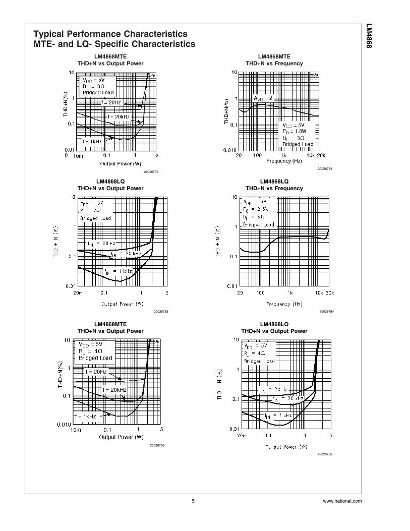
Typical Performance CharacteristicsMTE- and LQ- Specific Characteristics
LM4868MTETHD+N vs Output Power
LM4868MTETHD+N vs Frequency
2002673320026734
LM4868LQTHD+N vs Output Power
LM4868LQTHD+N vs Frequency
20026753 20026754
LM4868MTETHD+N vs Output Power
LM4868LQTHD+N vs Output Power
20026736
20026755
LM4868
www.national.com5
Typical Performance CharacteristicsMTE- and LQ- Specific Characteristics (Continued)
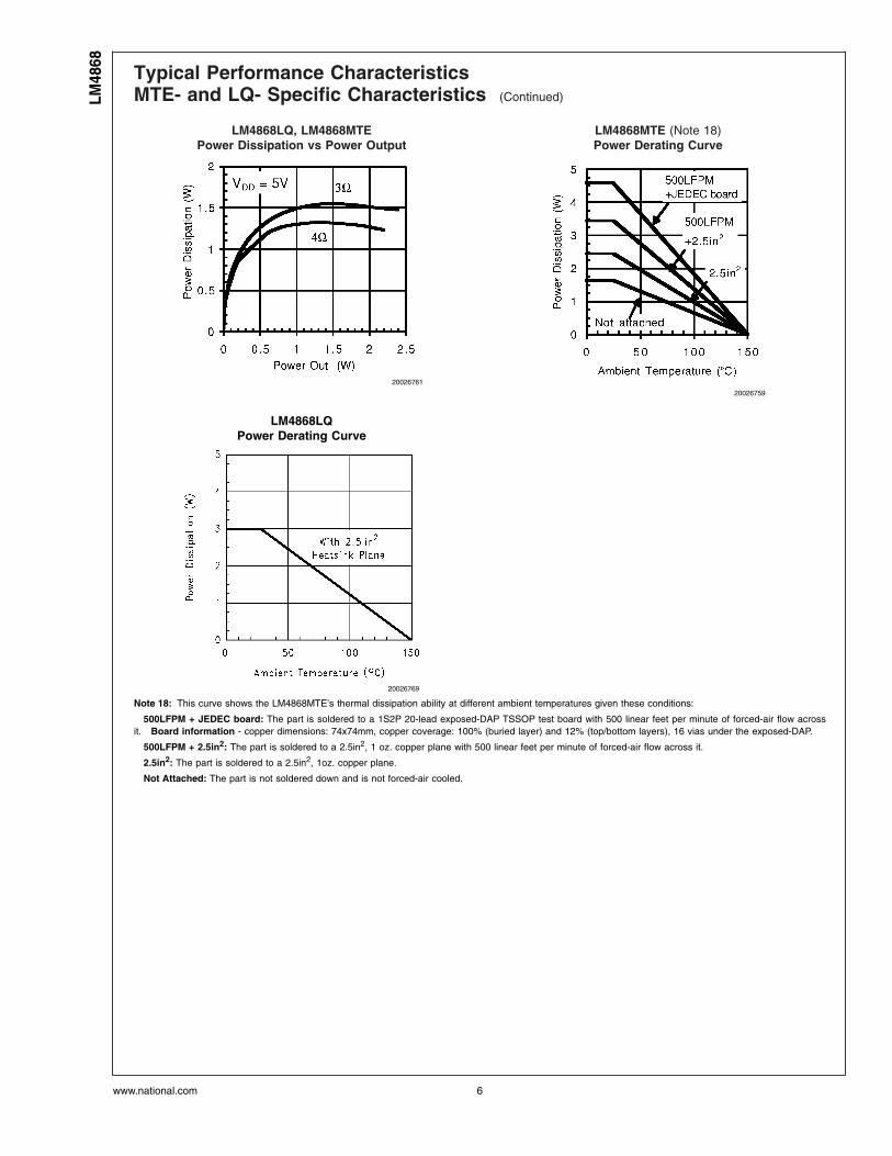
LM4868LQ, LM4868MTEPower Dissipation vs Power Output
LM4868MTE (Note 18)Power Derating Curve
20026761
20026759
LM4868LQPower Derating Curve
20026769
Note 18: This curve shows the LM4868MTE’s thermal dissipation ability at different ambient temperatures given these conditions:
500LFPM + JEDEC board: The part is soldered to a 1S2P 20-lead exposed-DAP TSSOP test board with 500 linear feet per minute of forced-air flow acrossit. Board information - copper dimensions: 74x74mm, copper coverage: 100% (buried layer) and 12% (top/bottom layers), 16 vias under the exposed-DAP.
500LFPM + 2.5in2: The part is soldered to a 2.5in2, 1 oz. copper plane with 500 linear feet per minute of forced-air flow across it.
2.5in2: The part is soldered to a 2.5in2, 1oz. copper plane.
Not Attached: The part is not soldered down and is not forced-air cooled.
LM48
68
www.national.com 6
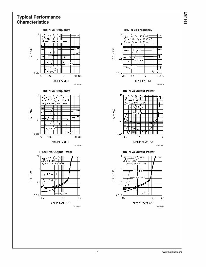
Typical PerformanceCharacteristics
THD+N vs Frequency THD+N vs Frequency
20026703 20026704
THD+N vs Frequency THD+N vs Output Power
20026705 20026706
THD+N vs Output Power THD+N vs Output Power
20026707 20026708
LM4868
www.national.com7
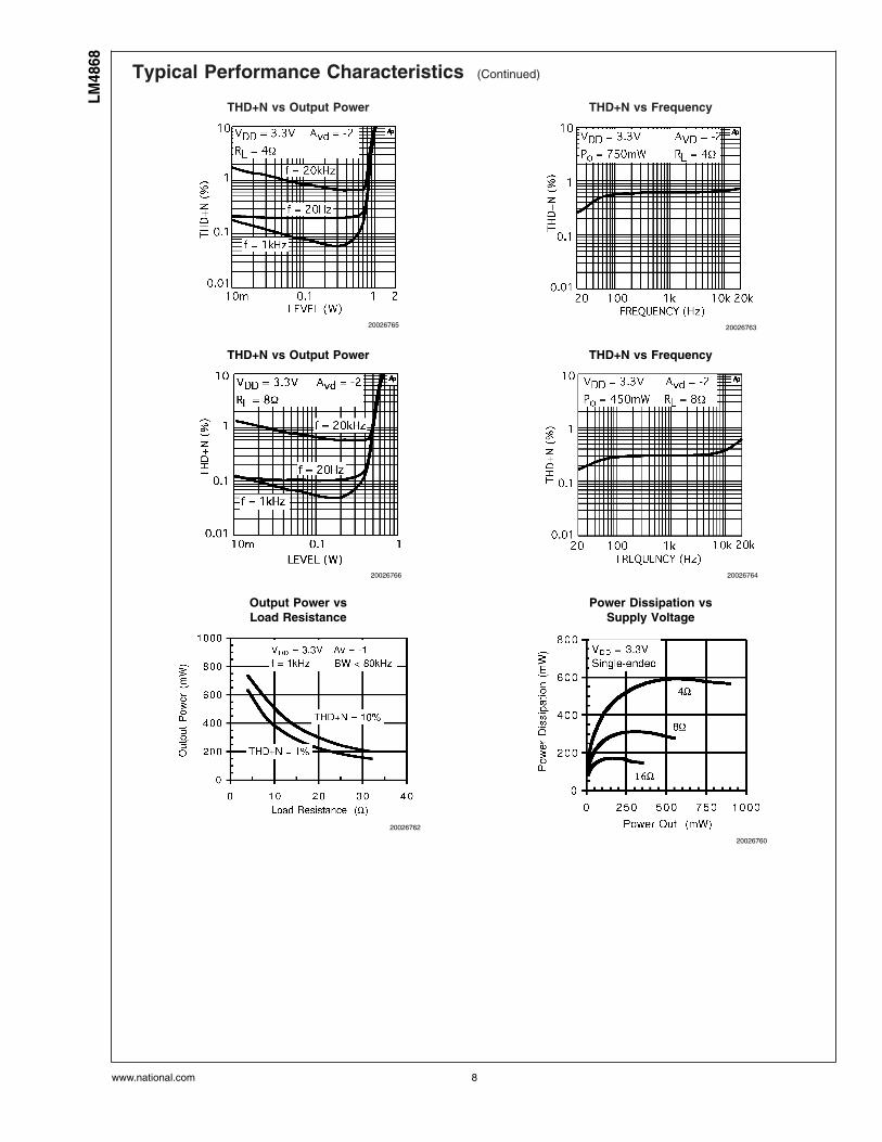
Typical Performance Characteristics (Continued)
THD+N vs Output Power THD+N vs Frequency
20026765 20026763
THD+N vs Output Power THD+N vs Frequency
20026766 20026764
Output Power vsLoad Resistance
Power Dissipation vsSupply Voltage
20026762
20026760
LM48
68
www.national.com 8
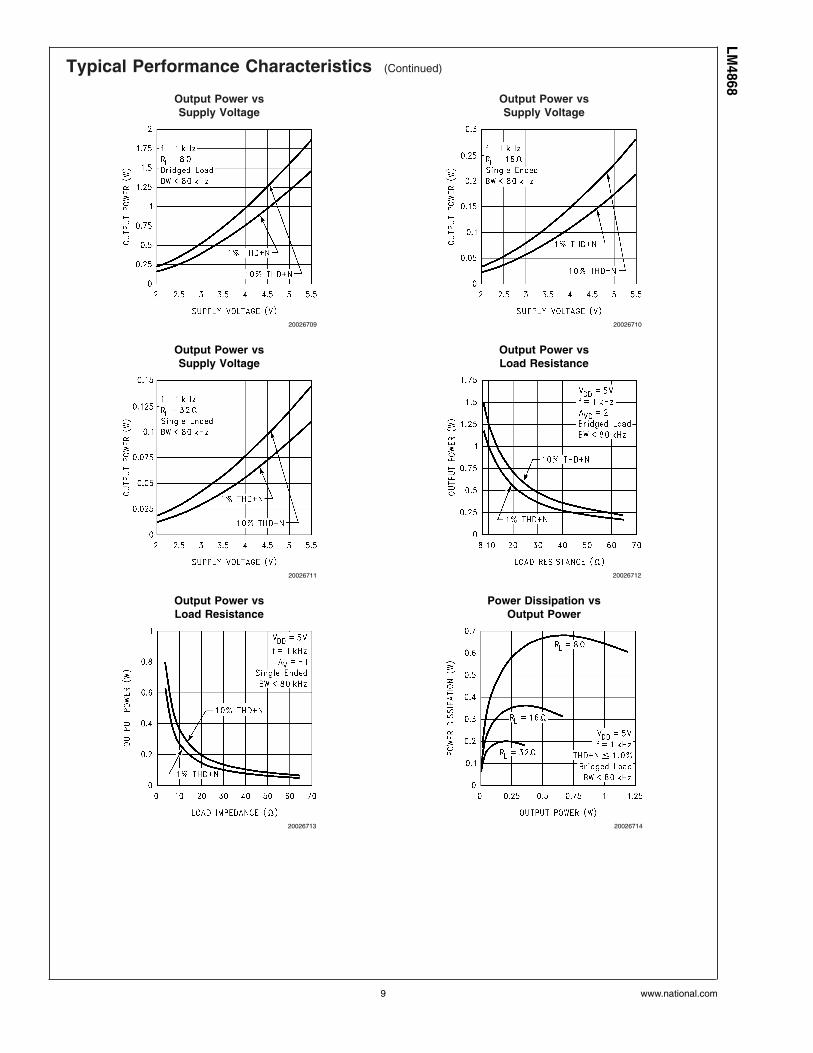
Typical Performance Characteristics (Continued)
Output Power vsSupply Voltage
Output Power vsSupply Voltage
20026709 20026710
Output Power vsSupply Voltage
Output Power vsLoad Resistance
20026711 20026712
Output Power vsLoad Resistance
Power Dissipation vsOutput Power
20026713 20026714
LM4868
www.national.com9
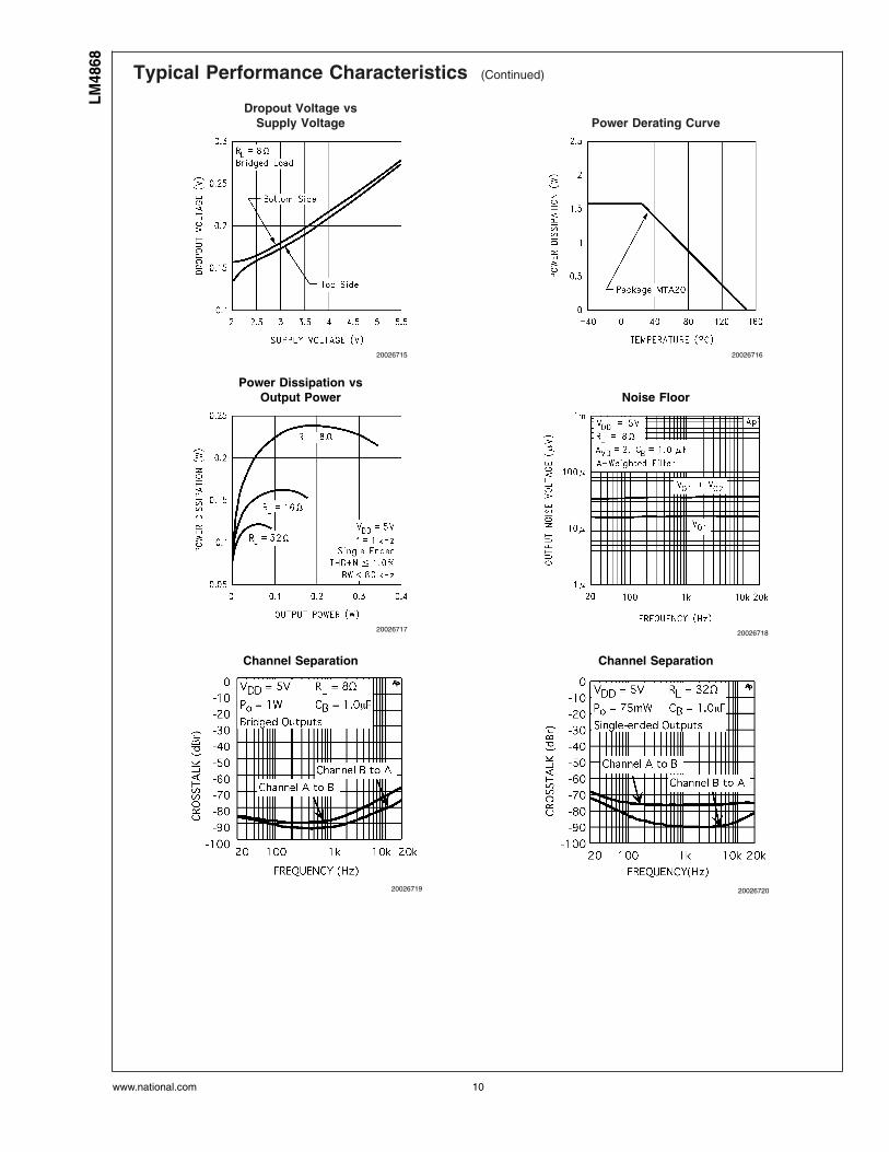
Typical Performance Characteristics (Continued)
Dropout Voltage vsSupply Voltage Power Derating Curve
20026715 20026716
Power Dissipation vsOutput Power Noise Floor
20026717 20026718
Channel Separation Channel Separation
20026719 20026720
LM48
68
www.national.com 10
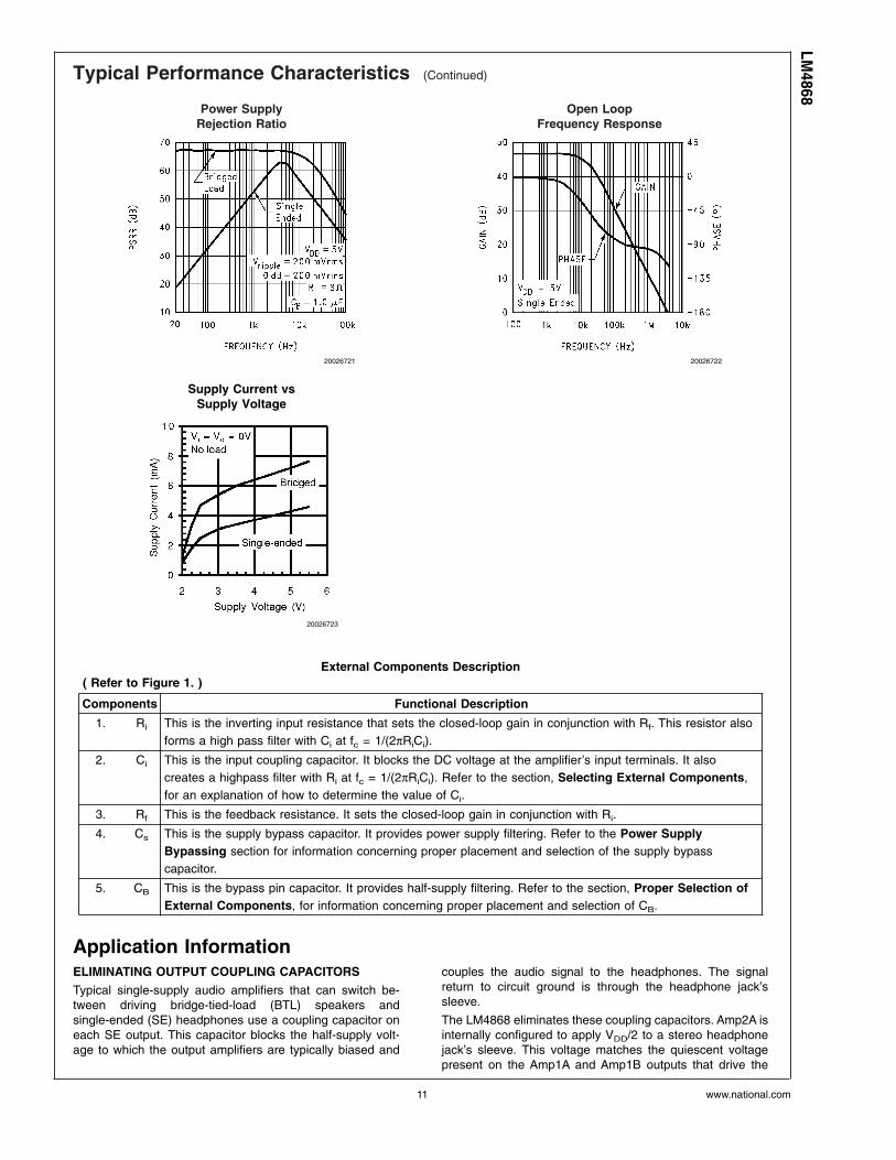
Typical Performance Characteristics (Continued)
Power SupplyRejection Ratio
Open LoopFrequency Response
20026721 20026722
Supply Current vsSupply Voltage
20026723
External Components Description( Refer to Figure 1. )
Components Functional Description
1. Ri This is the inverting input resistance that sets the closed-loop gain in conjunction with Rf. This resistor alsoforms a high pass filter with Ci at fc = 1/(2πRiCi).
2. Ci This is the input coupling capacitor. It blocks the DC voltage at the amplifier’s input terminals. It alsocreates a highpass filter with Ri at fc = 1/(2πRiCi). Refer to the section, Selecting External Components,for an explanation of how to determine the value of Ci.
3. Rf This is the feedback resistance. It sets the closed-loop gain in conjunction with Ri.
4. Cs This is the supply bypass capacitor. It provides power supply filtering. Refer to the Power SupplyBypassing section for information concerning proper placement and selection of the supply bypasscapacitor.
5. CB This is the bypass pin capacitor. It provides half-supply filtering. Refer to the section, Proper Selection ofExternal Components, for information concerning proper placement and selection of CB.
Application InformationELIMINATING OUTPUT COUPLING CAPACITORS
Typical single-supply audio amplifiers that can switch be-tween driving bridge-tied-load (BTL) speakers andsingle-ended (SE) headphones use a coupling capacitor oneach SE output. This capacitor blocks the half-supply volt-age to which the output amplifiers are typically biased and
couples the audio signal to the headphones. The signalreturn to circuit ground is through the headphone jack’ssleeve.
The LM4868 eliminates these coupling capacitors. Amp2A isinternally configured to apply VDD/2 to a stereo headphonejack’s sleeve. This voltage matches the quiescent voltagepresent on the Amp1A and Amp1B outputs that drive the
LM4868
www.national.com11
Application Information (Continued)
headphones. The headphones operate in a manner verysimilar to a bridge-tied-load (BTL). The same DC voltage isapplied to both headphone speaker terminals. This results inno net DC current flow through the speaker. AC current flowsthrough a headphone speaker as an audio signal’s outputamplitude increases on the speaker’s terminal.
When operating as a headphone amplifier, the headphonejack sleeve is not connected to circuit ground. Using theheadphone output jack as a line-level output will place theLM4868’s one-half supply voltage on a plug’s sleeve con-nection. Driving a portable notebook computer oraudio-visual display equipment is possible. This presents nodifficulty when the external equipment uses capacitivelycoupled inputs. For the very small minority of equipment thatis DC-coupled, the LM4868 monitors the current supplied bythe amplifier that drives the headphone jack’s sleeve. If thiscurrent exceeds 500mAPK, the amplifier is shutdown, pro-tecting the LM4868 and the external equipment. For moreinformation, see the section titled ’Single-Ended OutputPower Performance and Measurement Considerations’.
OUTPUT TRANSIENT (’POPS AND CLICKS’)ELIMINATED
The LM4868 contains advanced circuitry that eliminates out-put transients (’pop and click’). This circuitry prevents alltraces of transients when the supply voltage is first applied,when the part resumes operation after shutdown, or whenswitching between BTL speakers and SE headphones. Twocircuits combine to eliminate pop and click. One circuitmutes the output when switching between speaker loads.Another circuit monitors the input signal. It maintains themuted condition until there is sufficient input signal magni-tude (>25mVRMS, typ) to mask any remaining transient thatmay occur.
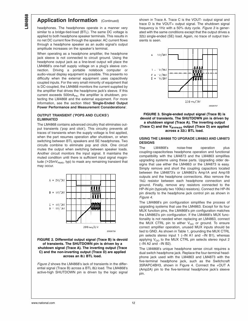
Figure 2 shows the LM4868’s lack of transients in the differ-ential signal (Trace B) across a BTL 8Ω load. The LM4868’sactive-high SHUTDOWN pin is driven by the logic signal
shown in Trace A. Trace C is the VOUT- output signal andtrace D is the VOUT+ output signal. The shutdown signalfrequency is 1Hz with a 50% duty cycle. Figure 3 is gener-ated with the same conditions except that the output drives a32Ω single-ended (SE) load. Again, no trace of output tran-sients is seen.
USING THE LM4868 TO UPGRADE LM4863 AND LM4873DESIGNS
The LM4868’s noise-free operation pluscoupling-capacitorless headphone operation and functionalcompatibility with the LM4873 and the LM4863 simplifiesupgrading systems using these parts. Upgrading older de-signs that use either the LM4863 or the LM4873 is easy.Simply remove and short the coupling capacitors locatedbetween the LM4873’s or LM4863’s Amp1A and Amp1Boutputs and the headphone connections. Also remove the1kΩ resistor between each headphone connection andground. Finally, remove any resistors connected to theHP-IN pin (typically two 100kΩ resistors). Connect the HP-INpin directly to the headphone jack control pin as shown inFigure 4.
The LM4868’s pin configuration simplifies the process ofupgrading systems that use the LM4863. Except for its fourMUX function pins, the LM4868’s pin configuration matchesthe LM4863’s pin configuration. If the LM4868’s MUX func-tionality is not needed when replacing an LM4863, connectthe MUX CTRL pin to either VDD or ground. To ensurecorrect amplifier operation, unused MUX inputs should betied to GND. As shown in Table 1, grounding the MUX CTRLpin selects stereo input 1 (−IN A1 and −IN B1), whereasapplying VDD to the MUX CTRL pin selects stereo input 2(−IN A2 and −IN B2).
The LM4868’s unique headphone sense circuit requires adual switch headphone jack. Replace the four-terminal head-phone jack used with the LM4863 and LM4873 with thefive-terminal headphone jack, such as the Switchcraft35RAPC4BH3, shown in Figure 4. Connect the +OUT A(Amp2A) pin to the five-terminal headphone jack’s sleevepin.
20026756
FIGURE 2. Differential output signal (Trace B) is devoidof transients. The SHUTDOWN pin is driven by a
shutdown signal (Trace A). The inverting output (TraceC) and the non-inverting output (Trace D) are applied
across an 8Ω BTL load.
20026757
FIGURE 3. Single-ended output signal (Trace B) isdevoid of transients. The SHUTDOWN pin is driven by
a shutdown signal (Trace A). The inverting output(Trace C) and the VBYPASS output (Trace D) are applied
across a 32Ω BTL load.
LM48
68
www.national.com 12
Application Information (Continued)
STEREO-INPUT MULTIPLEXER (STEREO MUX)
The LM4868 has two stereo inputs. The MUX CTRL Pincontrols which stereo input is active. As shown in the TruthTable for Logic Inputs, applying 0V to the MUX CTRL inputactivates stereo input 1, whereas applying VDD to the MUXCTRL inputs activates stereo input 2. To ensure correctamplifier operation, unused MUX inputs should be tied toGND.
Typical LM4868 applications use the MUX to switch betweentwo stereo input signals. Each stereo channel’s gain can betailored to produce the required output signal level by choos-ing the appropriate input and feedback resistor ratio.
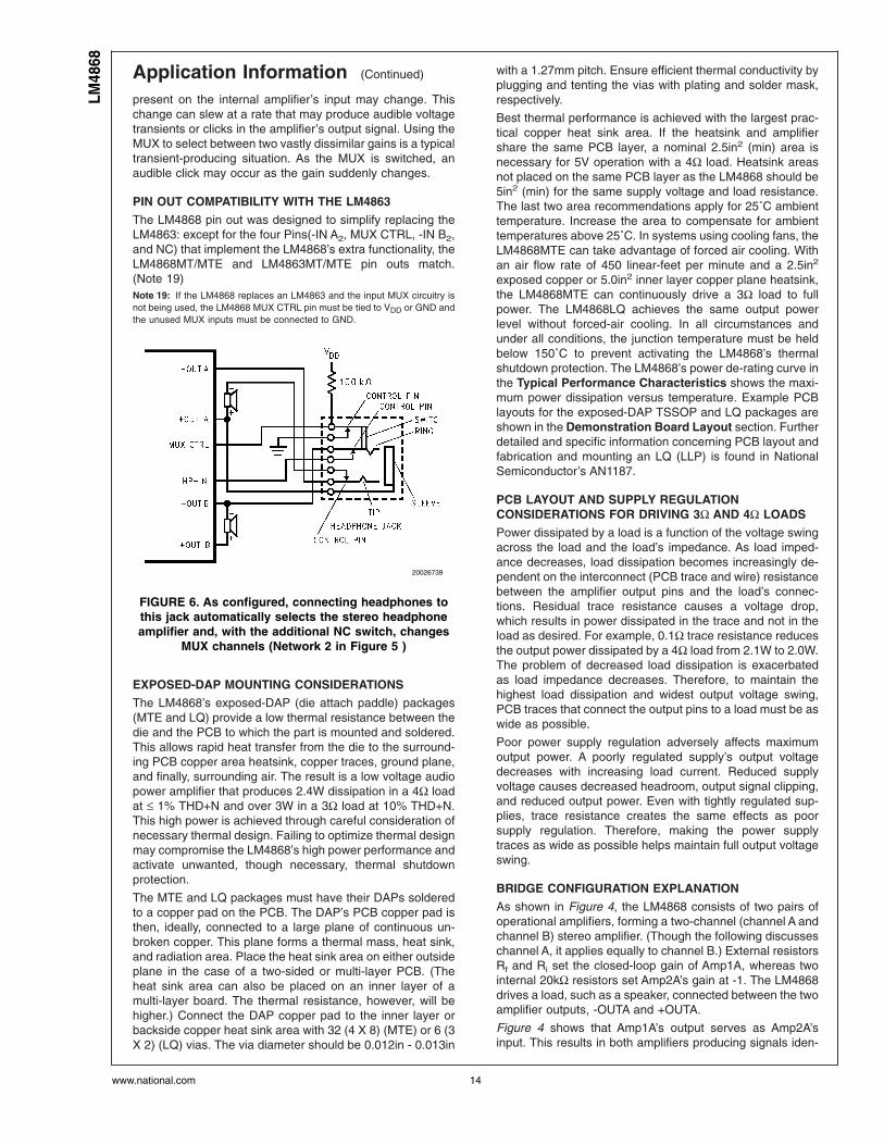
Another configuration uses the MUX to select two differentgains or frequency compensated gains that amplify a singlepair of stereo input signals. Figure 5 shows two differentfeedback networks, Network 1 and Network 2. Network 1produces increasing gain as the input signal’s frequencydecreases. This can be used to compensate a small,full-range speaker’s low frequency response roll-off. Network2 sets the gain for an alternate load such as headphones.The circuit in Figure 6 uses Network 1 when driving externalspeakers, switching to Network 2 when headphones areconnected. The normally closed control switch in Figure 6’sheadphone jack connects to the MUX CTRL pin. Whenheadphones are connected, the LM4868’s internal pull-upthat applies VDD to the HP-IN and the external 100kΩ resis-tor applies VDD to MUX CTRL pin. Simultaneously applyingthese control voltages automatically selects the amplifier(headphone or bridge) and switches the gain (MUX channelselection). Alternatively, leaving the MUX CTRL pin indepen-dently accessible allows a user to select bass boost asneeded. This alternative user-selectable bass-boost schemerequires connecting equal ratio resistor feedback networksto each MUX input channel. The value of the resistor in theRC network is chosen to give a gain that is necessary toachieve the desired bass-boost.
Switching between the MUX channels may change the inputsignal source or the feedback resistor network. During thechannel switching transition, the average voltage level
20026731
FIGURE 4. Typical Audio Amplifier Application Circuit(Pin out shown for the 24-pin Exposed-DAP LLP package. Numbers in ( ) are for the 20-pin MTE and MT packages.)
20026728
FIGURE 5. Input MUX Example
LM4868
www.national.com13
Application Information (Continued)
present on the internal amplifier’s input may change. Thischange can slew at a rate that may produce audible voltagetransients or clicks in the amplifier’s output signal. Using theMUX to select between two vastly dissimilar gains is a typicaltransient-producing situation. As the MUX is switched, anaudible click may occur as the gain suddenly changes.
PIN OUT COMPATIBILITY WITH THE LM4863
The LM4868 pin out was designed to simplify replacing theLM4863: except for the four Pins(-IN A2, MUX CTRL, -IN B2,and NC) that implement the LM4868’s extra functionality, theLM4868MT/MTE and LM4863MT/MTE pin outs match.(Note 19)Note 19: If the LM4868 replaces an LM4863 and the input MUX circuitry isnot being used, the LM4868 MUX CTRL pin must be tied to VDD or GND andthe unused MUX inputs must be connected to GND.
EXPOSED-DAP MOUNTING CONSIDERATIONS
The LM4868’s exposed-DAP (die attach paddle) packages(MTE and LQ) provide a low thermal resistance between thedie and the PCB to which the part is mounted and soldered.This allows rapid heat transfer from the die to the surround-ing PCB copper area heatsink, copper traces, ground plane,and finally, surrounding air. The result is a low voltage audiopower amplifier that produces 2.4W dissipation in a 4Ω loadat ≤ 1% THD+N and over 3W in a 3Ω load at 10% THD+N.This high power is achieved through careful consideration ofnecessary thermal design. Failing to optimize thermal designmay compromise the LM4868’s high power performance andactivate unwanted, though necessary, thermal shutdownprotection.
The MTE and LQ packages must have their DAPs solderedto a copper pad on the PCB. The DAP’s PCB copper pad isthen, ideally, connected to a large plane of continuous un-broken copper. This plane forms a thermal mass, heat sink,and radiation area. Place the heat sink area on either outsideplane in the case of a two-sided or multi-layer PCB. (Theheat sink area can also be placed on an inner layer of amulti-layer board. The thermal resistance, however, will behigher.) Connect the DAP copper pad to the inner layer orbackside copper heat sink area with 32 (4 X 8) (MTE) or 6 (3X 2) (LQ) vias. The via diameter should be 0.012in - 0.013in
with a 1.27mm pitch. Ensure efficient thermal conductivity byplugging and tenting the vias with plating and solder mask,respectively.
Best thermal performance is achieved with the largest prac-tical copper heat sink area. If the heatsink and amplifiershare the same PCB layer, a nominal 2.5in2 (min) area isnecessary for 5V operation with a 4Ω load. Heatsink areasnot placed on the same PCB layer as the LM4868 should be5in2 (min) for the same supply voltage and load resistance.The last two area recommendations apply for 25˚C ambienttemperature. Increase the area to compensate for ambienttemperatures above 25˚C. In systems using cooling fans, theLM4868MTE can take advantage of forced air cooling. Withan air flow rate of 450 linear-feet per minute and a 2.5in2
exposed copper or 5.0in2 inner layer copper plane heatsink,the LM4868MTE can continuously drive a 3Ω load to fullpower. The LM4868LQ achieves the same output powerlevel without forced-air cooling. In all circumstances andunder all conditions, the junction temperature must be heldbelow 150˚C to prevent activating the LM4868’s thermalshutdown protection. The LM4868’s power de-rating curve inthe Typical Performance Characteristics shows the maxi-mum power dissipation versus temperature. Example PCBlayouts for the exposed-DAP TSSOP and LQ packages areshown in the Demonstration Board Layout section. Furtherdetailed and specific information concerning PCB layout andfabrication and mounting an LQ (LLP) is found in NationalSemiconductor’s AN1187.
PCB LAYOUT AND SUPPLY REGULATIONCONSIDERATIONS FOR DRIVING 3Ω AND 4Ω LOADS
Power dissipated by a load is a function of the voltage swingacross the load and the load’s impedance. As load imped-ance decreases, load dissipation becomes increasingly de-pendent on the interconnect (PCB trace and wire) resistancebetween the amplifier output pins and the load’s connec-tions. Residual trace resistance causes a voltage drop,which results in power dissipated in the trace and not in theload as desired. For example, 0.1Ω trace resistance reducesthe output power dissipated by a 4Ω load from 2.1W to 2.0W.The problem of decreased load dissipation is exacerbatedas load impedance decreases. Therefore, to maintain thehighest load dissipation and widest output voltage swing,PCB traces that connect the output pins to a load must be aswide as possible.
Poor power supply regulation adversely affects maximumoutput power. A poorly regulated supply’s output voltagedecreases with increasing load current. Reduced supplyvoltage causes decreased headroom, output signal clipping,and reduced output power. Even with tightly regulated sup-plies, trace resistance creates the same effects as poorsupply regulation. Therefore, making the power supplytraces as wide as possible helps maintain full output voltageswing.
BRIDGE CONFIGURATION EXPLANATION
As shown in Figure 4, the LM4868 consists of two pairs ofoperational amplifiers, forming a two-channel (channel A andchannel B) stereo amplifier. (Though the following discusseschannel A, it applies equally to channel B.) External resistorsRf and Ri set the closed-loop gain of Amp1A, whereas twointernal 20kΩ resistors set Amp2A’s gain at -1. The LM4868drives a load, such as a speaker, connected between the twoamplifier outputs, -OUTA and +OUTA.
Figure 4 shows that Amp1A’s output serves as Amp2A’sinput. This results in both amplifiers producing signals iden-
20026739
FIGURE 6. As configured, connecting headphones tothis jack automatically selects the stereo headphoneamplifier and, with the additional NC switch, changes
MUX channels (Network 2 in Figure 5 )
LM48
68
www.national.com 14
Application Information (Continued)
tical in magnitude, but 180˚ out of phase. Taking advantageof this phase difference, a load is placed between -OUTAand +OUTA and driven differentially (’commonly referred toas bridge mode’). This results in a differential gain of
AVD = 2 * (Rf/R i) (1)
Bridge mode amplifiers are different from single-ended am-plifiers that drive loads connected between a single amplifi-er’s output and ground. For a given supply voltage, bridgemode has a distinct advantage over the single-ended con-figuration: its differential output doubles the voltage swingacross the load. This produces four times the output powerwhen compared to a single-ended amplifier under the sameconditions. This increase in attainable output power as-sumes that the amplifier is not current limited or that theoutput signal is not clipped. To ensure minimum output sig-nal clipping when choosing an amplifier’s closed-loop gain,refer to the Audio Power Amplifier Design section.
Another advantage of the differential bridge output is no netDC voltage across the load. This is accomplished by biasingchannel A’s and channel B’s outputs at half-supply. Thiseliminates the coupling capacitor that single supply,single-ended amplifiers require. Eliminating an output cou-pling capacitor in a single-ended configuration forces asingle-supply amplifier’s half-supply bias voltage across theload. This increases internal IC power dissipation and maypermanently damage loads such as speakers.
POWER DISSIPATION
Power dissipation is a major concern when designing asuccessful single-ended or bridged amplifier. Equation (2)states the maximum power dissipation point for asingle-ended amplifier operating at a given supply voltageand driving a specified output load.
PDMAX = (VDD)2/(2π2RL): Single-Ended (2)
However, a direct consequence of the increased power de-livered to the load by a bridge amplifier is higher internalpower dissipation for the same conditions.
The LM4868 has two operational amplifiers per channel. Themaximum internal power dissipation per channel operating inthe bridge mode is four times that of a single-ended ampli-fier. From Equation (3), assuming a 5V power supply and an4Ω load, the maximum single channel power dissipation is1.27W or 2.54W for stereo operation.
PDMAX = 4 * (VDD)2/(2π2RL): Bridge Mode (3)
The LM4868’s power dissipation is twice that given by Equa-tion (2) or Equation (3) when operating in the single-endedmode or bridge mode, respectively. Twice the maximumpower dissipation point given by Equation (3) must not ex-ceed the power dissipation given by Equation (4):
PDMAX’ = (TJMAX − TA)/θJA (4)
The LM4868’s TJMAX = 150˚C. In the LQ package solderedto a DAP pad that expands to a copper area of 5in2 on aPCB, the LM4868’s θJA is 42˚C/W. In the MTE package
soldered to a DAP pad that expands to a copper area of 2in2
on a PCB, the LM4868’s θJA is 41˚C/W. At any given ambienttemperature TA, use Equation (4) to find the maximum inter-nal power dissipation supported by the IC packaging. Rear-ranging Equation (4) and substituting PDMAX for PDMAX’ re-sults in Equation (5). This equation gives the maximumambient temperature that still allows maximum stereo powerdissipation without violating the LM4868’s maximum junctiontemperature.
TA = TJMAX − 2 X PDMAX θJA (5)
For a typical application with a 5V power supply and an 4Ωload, the maximum ambient temperature that allows maxi-mum stereo power dissipation without exceeding the maxi-mum junction temperature is approximately 43˚C for the LQpackage and 45˚C for the MTE package.
TJMAX = PDMAX θJA + TA (6)
Equation (6) gives the maximum junction temperatureTJMAX. If the result violates the LM4868’s 150˚C, reduce themaximum junction temperature by reducing the power sup-ply voltage or increasing the load resistance. Further allow-ance should be made for increased ambient temperatures.
The above examples assume that a device is a surfacemount part operating around the maximum power dissipationpoint. Since internal power dissipation is a function of outputpower, higher ambient temperatures are allowed as outputpower or duty cycle decreases.
If the result of Equation (2) is greater than that of Equation(3), then decrease the supply voltage, increase the loadimpedance, or reduce the ambient temperature. If thesemeasures are insufficient, a heat sink can be added toreduce θJA. The heat sink can be created using additionalcopper area around the package, with connections to theground pin(s), supply pin and amplifier output pins. External,solder attached SMT heatsinks such as the Thermalloy7106D can also improve power dissipation. When adding aheat sink, the θJA is the sum of θJC, θCS, and θSA. (θJC is thejunction−to−case thermal impedance, θCS is thecase−to−sink thermal impedance, and θSA is thesink−to−ambient thermal impedance.) Refer to the TypicalPerformance Characteristics curves for power dissipationinformation at lower output power levels.
POWER SUPPLY BYPASSING
As with any power amplifier, proper supply bypassing iscritical for low noise performance and high power supplyrejection. Applications that employ a 5V regulator typicallyuse a 10µF in parallel with a 0.1µF filter capacitors to stabi-lize the regulator’s output, reduce noise on the supply line,and improve the supply’s transient response. However, theirpresence does not eliminate the need for a local 1.0µFtantalum bypass capacitance connected between theLM4868’s supply pins and ground. Do not substitute a ce-ramic capacitor for the tantalum. Doing so may cause oscil-lation. Keep the length of leads and traces that connectcapacitors between the LM4868’s power supply pin andground as short as possible. Connecting a 1µF capacitor,CB, between the BYPASS pin and ground improves theinternal bias voltage’s stability and improves the amplifier’sPSRR. The PSRR improvements increase as the bypass pincapacitor value increases. Too large, however, increasesturn−on time and can compromise the amplifier’s click and
LM4868
www.national.com15
Application Information (Continued)
pop performance. The selection of bypass capacitor values,especially CB, depends on desired PSRR requirements,click and pop performance (as explained in the section,Proper Selection of External Components), system cost,and size constraints.
MICRO−POWER SHUTDOWN
The voltage applied to the SHUTDOWN pin controls theLM4868’s shutdown function. Activate micro−power shut-down by applying VDD to the SHUTDOWN pin. When active,the LM4868’s micro−power shutdown feature turns off theamplifier’s bias circuitry, reducing the supply current. Thelogic threshold is typically VDD/2. The low 0.7µA typicalshutdown current is achieved by applying a voltage that is asnear as VDD as possible to the SHUTDOWN pin. A voltagethat is less than VDD may increase the shutdown current.Table 1 shows the logic signal levels that activate and deac-tivate micro−power shutdown and headphone amplifier op-
eration. To ensure that the output signal remainstransient−free, do not cycle the shutdown functionfaster than 1Hz.
There are a few ways to control the micro−power shutdown.These include using a single−pole, single, throw switch, amicroprocessor, or a microcontroller. When using a switch,connect an external 100kΩ pull−up resistor between theSHUTDOWN pin and VDD. Connect the switch between theSHUTDOWN pin and ground. Select normal amplifier opera-tion by closing the switch. Opening the switch connects theSHUTDOWN pin to VDD through the pull−up resistor, acti-vating micro−power shutdown. The switch and resistor guar-antee that the SHUTDOWN pin will not float. This preventsunwanted state changes. In a system with a microprocessoror a microcontroller, use a digital output to apply the controlvoltage to the SHUTDOWN pin. Driving the SHUTDOWN pinwith active circuitry eliminates the pull up resistor.
Truth Table for Logic Inputs
SHUTDOWNPIN
HP-INPIN
MUX CHANNELINPUT SELECT
OPERATIONAL MODE (MUXINPUTCHANNEL #)
Logic Low = −OUTB signal Logic Low Bridged amplifiers (1)
Logic Low = −OUTB signal Logic High Bridged amplifiers (2)
Logic Low ≠ −OUTB signal Logic Low Single-ended amplifiers (1)
Logic Low ≠ −OUTB signal Logic High Single-ended amplifiers (2)
Logic High X X Micro−power shutdown
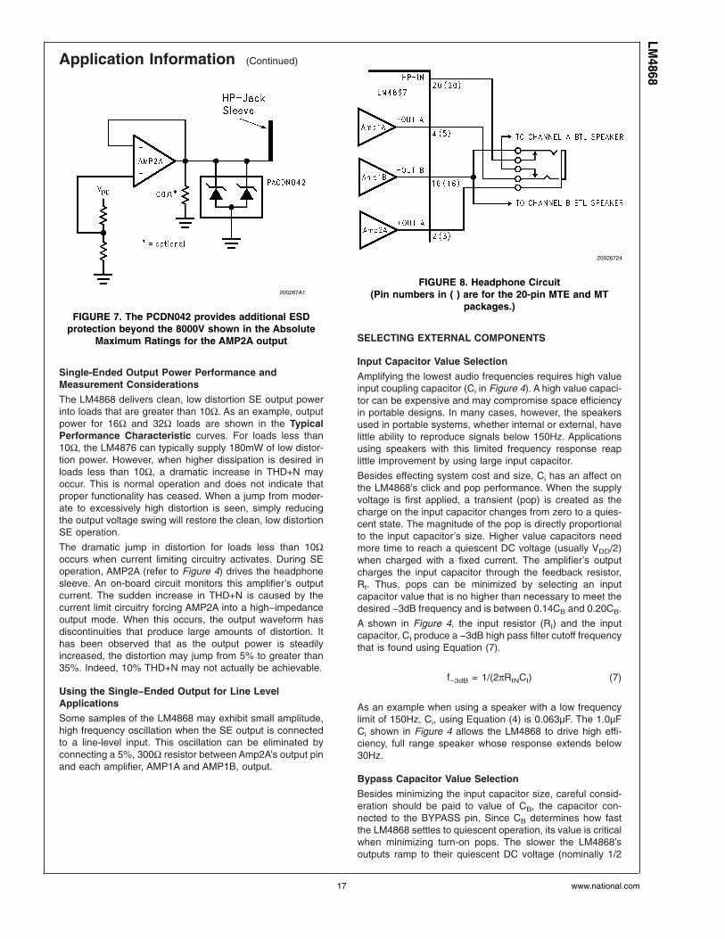
HEADPHONE (SINGLE-ENDED) AMPLIFIEROPERATION
An internal pull−up circuit is connected to the HP−IN (pin 20)headphone amplifier control pin. When this pin is left uncon-nected, VDD is applied to the HP−IN. This turns off Amp2Band switches Amp2A’s input signal from an audio signal tothe VDD/2 voltage present on pin 14. The result is mutedbridge-connected loads. Quiescent current consumption isreduced when the IC is in this single−ended mode.
Figure 8 shows the implementation of the LM4868’s head-phone control function. An internal comparator with a nomi-nal 400mV offset monitors the signal present at the −OUTBoutput. It compares this signal against the signal applied tothe HP−IN pin. When these signals are equal, as is the casewhen a BTL is connected to the amplifier, the comparatorforces the LM4868 to maintain bridged−amplifier operation.When the HP−IN pin is externally floated, such as whenheadphones are connected to the jack shown in Figure 8,and internal pull−up forces VDD on the internal comparator’sHP−IN inputs. This changes the comparator’s output stateand enables the headphone function: it turns off Amp2B,switches Amp2A’s input signal from an audio signal to theVDD/2 voltage present on pin 14, and mutes thebridge-connected loads. Amp1A and Amp1B drive the head-phones.
Figure 8 also shows the suggested headphone jack electri-cal connections. The jack is designed to mate with athree−wire plug. The plug’s tip and ring should each carryone of the two stereo output signals, whereas the sleeve
provides the return to Amp2A. A headphone jack with onecontrol pin contact is sufficient to drive the HP−IN pin whenconnecting headphones.
A switch can replace the headphone jack contact pin. Whena switch shorts the HP−IN pin to VDD, bridge−connectedspeakers are muted and Amp1A and Amp2A drive a pair ofheadphones. When a switch shorts the HP−IN pin to GND,the LM4868 operates in bridge mode. If headphone drive isnot needed, short the HP−IN pin to the −OUTB pin.
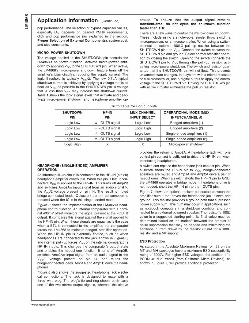
Figure 7 shows an optional resistor connected between theamplifier output that drives the headphone jack sleeve andground. This resistor provides a ground path that supressedpower supply hum. This hum may occur in applications suchas notebook computers in a shutdown condition and con-nected to an external powered speaker. The resistor’s 100Ωvalue is a suggested starting point. Its final value must bedetermined based on the tradeoff between the amount ofnoise suppression that may be needed and minimizing theadditional current drawn by the resistor (25mA for a 100Ωresistor and a 5V supply).
ESD Protection
As stated in the Absolute Maximum Ratings, pin 28 on theMT and MH packages have a maximum ESD susceptibilityrating of 8000V. For higher ESD voltages, the addition of aPCDN042 dual transil (from California Micro Devices), asshown in Figure 7, will provide additional protection.
LM48
68
www.national.com 16
Application Information (Continued)
Single-Ended Output Power Performance andMeasurement Considerations
The LM4868 delivers clean, low distortion SE output powerinto loads that are greater than 10Ω. As an example, outputpower for 16Ω and 32Ω loads are shown in the TypicalPerformance Characteristic curves. For loads less than10Ω, the LM4876 can typically supply 180mW of low distor-tion power. However, when higher dissipation is desired inloads less than 10Ω, a dramatic increase in THD+N mayoccur. This is normal operation and does not indicate thatproper functionality has ceased. When a jump from moder-ate to excessively high distortion is seen, simply reducingthe output voltage swing will restore the clean, low distortionSE operation.
The dramatic jump in distortion for loads less than 10Ωoccurs when current limiting circuitry activates. During SEoperation, AMP2A (refer to Figure 4) drives the headphonesleeve. An on-board circuit monitors this amplifier’s outputcurrent. The sudden increase in THD+N is caused by thecurrent limit circuitry forcing AMP2A into a high−impedanceoutput mode. When this occurs, the output waveform hasdiscontinuities that produce large amounts of distortion. Ithas been observed that as the output power is steadilyincreased, the distortion may jump from 5% to greater than35%. Indeed, 10% THD+N may not actually be achievable.
Using the Single−Ended Output for Line LevelApplications
Some samples of the LM4868 may exhibit small amplitude,high frequency oscillation when the SE output is connectedto a line-level input. This oscillation can be eliminated byconnecting a 5%, 300Ω resistor between Amp2A’s output pinand each amplifier, AMP1A and AMP1B, output.
SELECTING EXTERNAL COMPONENTS
Input Capacitor Value Selection
Amplifying the lowest audio frequencies requires high valueinput coupling capacitor (Ci in Figure 4). A high value capaci-tor can be expensive and may compromise space efficiencyin portable designs. In many cases, however, the speakersused in portable systems, whether internal or external, havelittle ability to reproduce signals below 150Hz. Applicationsusing speakers with this limited frequency response reaplittle improvement by using large input capacitor.
Besides effecting system cost and size, Ci has an affect onthe LM4868’s click and pop performance. When the supplyvoltage is first applied, a transient (pop) is created as thecharge on the input capacitor changes from zero to a quies-cent state. The magnitude of the pop is directly proportionalto the input capacitor’s size. Higher value capacitors needmore time to reach a quiescent DC voltage (usually VDD/2)when charged with a fixed current. The amplifier’s outputcharges the input capacitor through the feedback resistor,Rf. Thus, pops can be minimized by selecting an inputcapacitor value that is no higher than necessary to meet thedesired −3dB frequency and is between 0.14CB and 0.20CB.
A shown in Figure 4, the input resistor (RI) and the inputcapacitor, CI produce a −3dB high pass filter cutoff frequencythat is found using Equation (7).
f−3dB = 1/(2πRINCI) (7)
As an example when using a speaker with a low frequencylimit of 150Hz, Ci, using Equation (4) is 0.063µF. The 1.0µFCi shown in Figure 4 allows the LM4868 to drive high effi-ciency, full range speaker whose response extends below30Hz.
Bypass Capacitor Value Selection
Besides minimizing the input capacitor size, careful consid-eration should be paid to value of CB, the capacitor con-nected to the BYPASS pin. Since CB determines how fastthe LM4868 settles to quiescent operation, its value is criticalwhen minimizing turn-on pops. The slower the LM4868’soutputs ramp to their quiescent DC voltage (nominally 1/2
200267A1
FIGURE 7. The PCDN042 provides additional ESDprotection beyond the 8000V shown in the Absolute
Maximum Ratings for the AMP2A output
20026724
FIGURE 8. Headphone Circuit(Pin numbers in ( ) are for the 20-pin MTE and MT
packages.)
LM4868
www.national.com17
Application Information (Continued)
VDD), the smaller the turn-on pop. Choosing CB equal to1.0µF along with a small value of Ci (in the range of 0.1µF to0.39µF), produces a click-less and pop-less shutdown func-tion. As discussed above, choosing Ci no larger than neces-sary for the desired bandwidth helps minimize clicks andpops. CB’s value should be in the range of 5 times to 7 timesthe value of Ci. This ensures that output transients areeliminated when power is first applied or the LM4868 re-sumes operation after shutdown.
OPTIMIZING CLICK AND POP REDUCTIONPERFORMANCE
The LM4868 contains circuitry that eliminates turn-on andshutdown transients (“clicks and pops“) and transients thatcould occur when switching between BTL speakers andsingle-ended headphones. For this discussion, turn-on re-fers to either applying the power supply voltage or when theshutdown mode is deactivated. While the power supply isramping to its final value, the LM4868’s internal amplifiersare configured as unity gain buffers and are disconnectedfrom the -OUT and +OUT pins. An internal current sourcechanges the voltage of the BYPASS pin in a controlled,linear manner. Ideally, the input and outputs track the voltageapplied to the BYPASS pin. The gain of the internal amplifi-ers remains unity until the voltage on the bypass pin reaches1/2 VDD. As soon as the voltage on the bypass pin is stable,the device becomes fully operational and the amplifier out-puts are reconnected to the -OUT and +OUT pins. Althoughthe BYPASS pin current cannot be modified, changing thesize of CB alters the device’s turn-on time. There is a linearrelationship between the size of CB and the turn-on time.Here are some typical turn-on times for various values of CB:
CB TON
0.01µF 3ms
0.1µF 30ms
0.22µF 63ms
0.47µF 134ms
1.0µF 300ms
2.2µF 630ms
In order eliminate “clicks and pops“, all capacitors must bedischarged before turn-on. Rapidly switching VDD may notallow the capacitors to fully discharge, which may cause“clicks and pops“.
NO LOAD STABILITY
The LM4868 may exhibit low level oscillation when the loadresistance is greater than 10kΩ. This oscillation only occursas the output signal swings near the supply voltages. Pre-vent this oscillation by connecting a 5kΩ between the outputpins and ground.
AUDIO POWER AMPLIFIER DESIGN
Audio Amplifier Design: Driving 1W into an 8Ω Load
The following are the desired operational parameters:
Power Output: 1 WRMS
Load Impedance: 8Ω
Input Level: 1 VRMS
Input Impedance: 20 kΩBandwidth: 100 Hz−20 kHz ± 0.25 dB
The design begins by specifying the minimum supply voltagenecessary to obtain the specified output power. One way tofind the minimum supply voltage is to use the Output Powervs Supply Voltage curve in the Typical Performance Char-acteristics section. Another way, using Equation (8), is tocalculate the peak output voltage necessary to achieve thedesired output power for a given load impedance. To ac-count for the amplifier’s dropout voltage, two additional volt-ages, based on the Dropout Voltage vs Supply Voltage in theTypical Performance Characteristics curves, must beadded to the result obtained by Equation (8). The result isEquation (9).
(8)
VDD ≥ (VOUTPEAK+ (VODTOP+ VODBOT
)) (9)
The Output Power vs Supply Voltage graph for an 8Ω loadindicates a minimum supply voltage of 4.6V. This is easilymet by the commonly used 5V supply voltage. The additionalvoltage creates the benefit of headroom, allowing theLM4868 to produce peak output power in excess of 1Wwithout clipping or other audible distortion. The choice ofsupply voltage must also not create a situation that violatesof maximum power dissipation as explained above in thePower Dissipation section.
After satisfying the LM4868’s power dissipation require-ments, the minimum differential gain needed to achieve 1Wdissipation in an 8Ω load is found using Equation (10).
(10)
Thus, a minimum gain of 2.83 allows the LM4868’s to reachfull output swing and maintain low noise and THD+N perfor-mance. For this example, let AVD = 3.
The amplifier’s overall gain is set using the input (Ri) andfeedback (Ri) resistors. With the desired input impedanceset at 20kΩ, the feedback resistor is found using Equation(11).
Rf/Ri = AVD/2 (11)
The value of Rf is 30kΩ.
The last step in this design example is setting the amplifier’s−3dB frequency bandwidth. To achieve the desired ±0.25dBpass band magnitude variation limit, the low frequency re-sponse must extend to at least one-fifth the lower bandwidthlimit and the high frequency response must extend to at leastfive times the upper bandwidth limit. The gain variation forboth response limits is 0.17dB, well within the ±0.25dBdesired limit. The results are an
LM48
68
www.national.com 18
Application Information (Continued)
fL = 100Hz/5 = 20Hz (12)
and an
fH = 20kHz x 5 = 100kHz (13)
As mentioned in the Selecting Proper External Compo-nents section, Ri and Ci create a highpass filter that sets theamplifier’s lower bandpass frequency limit. Find the couplingcapacitor’s value using Equation (12).
Ci≥ 1/(2πR ifL) (14)
The result is
1/(2π*20kΩ*20Hz) = 0.397µF (15)
Use a 0.39µF capacitor, the closest standard value.
The product of the desired high frequency cutoff (100kHz inthis example) and the differential gain AVD, determines the
upper passband response limit. With AVD = 3 and fH =100kHz, the closed-loop gain bandwidth product (GBWP) is300kHz. This is less than the LM4868’s 3.5MHz GBWP. Withthis margin, the amplifier can be used in designs that requiremore differential gain while avoiding performance,restrictingbandwidth limitations.
RECOMMENDED PRINTED CIRCUIT BOARD LAYOUT
Figures 9 through 13 show the recommended four-layer PCboard layout that is optimized for the 24-pin LQ-packagedLM4868 and associated external components. Figures 14through 18 show the recommended four-layer PC boardlayout that is optimized for the 24-pin MTE-packagedLM4868 and associated external components. Figures 19through 21 show the recommended two-layer PC boardlayout that is optimized for the 20-pin MT-packaged LM4868and associated external components. These circuits are de-signed for use with an external 5V supply and 4Ω speakers(or greater) for the MT-packaged LM4868 or 3Ω speakers (orgreater) for the LQ- and MTE-packaged LM4868.
These circuit boards are easy to use. Apply 5V and ground tothe board’s VDD and GND pads, respectively. Connect 4Ωspeakers between the board’s −OUTA and +OUTA andOUTB and +OUTB pads.
20026778
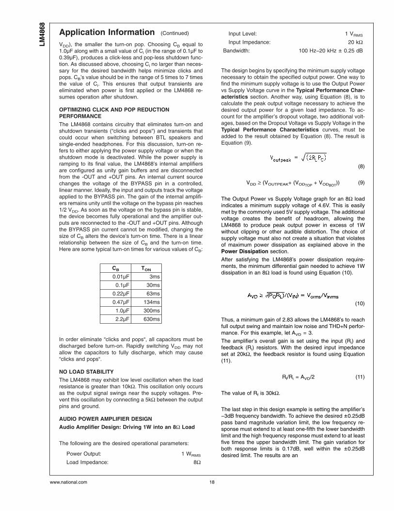
FIGURE 9. Recommended LQ PC Board Layout:Component-Side Silkscreen
LM4868
www.national.com19
Application Information (Continued)
20026741
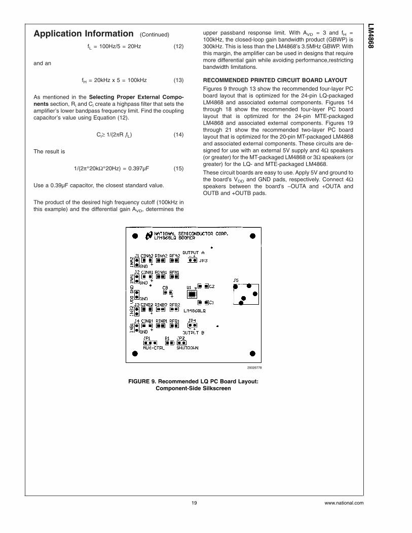
FIGURE 10. Recommended LQ PC Board Layout:Component-Side Layout
20026742
FIGURE 11. Recommended LQ PC Board Layout:Upper Inner-Layer Layout
LM48
68
www.national.com 20
Application Information (Continued)
20026743
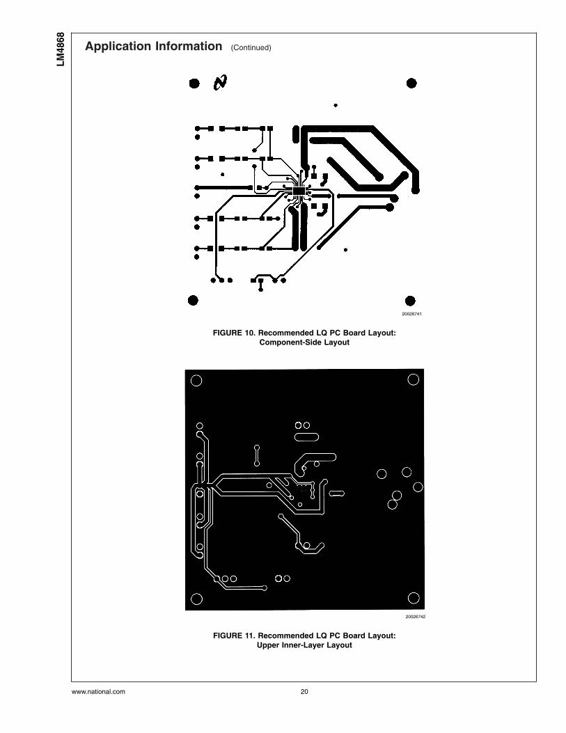
FIGURE 12. Recommended LQ PC Board Layout:Lower Inner-Layer Layout
20026744
FIGURE 13. Recommended LQ PC Board Layout:Bottom-Side Layout
LM4868
www.national.com21
Application Information (Continued)
20026770
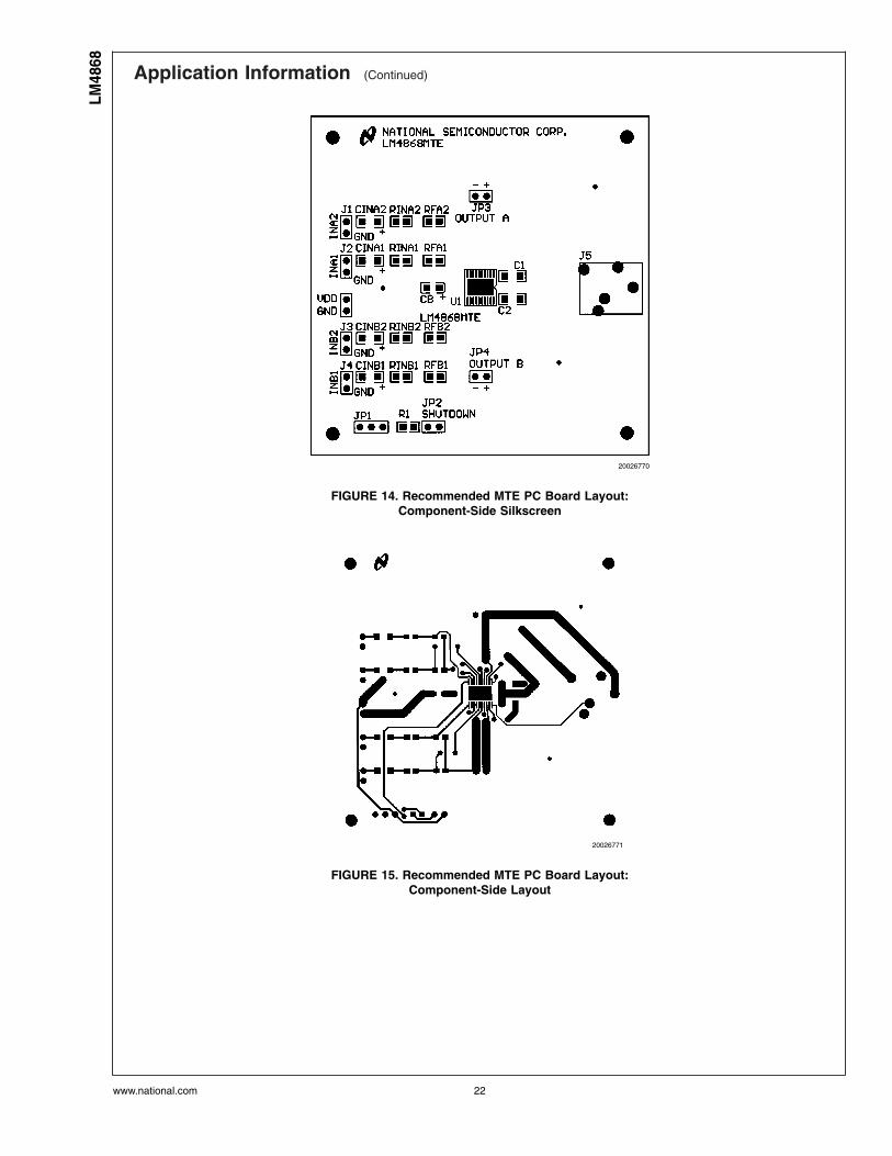
FIGURE 14. Recommended MTE PC Board Layout:Component-Side Silkscreen
20026771
FIGURE 15. Recommended MTE PC Board Layout:Component-Side Layout
LM48
68
www.national.com 22
Application Information (Continued)
20026772
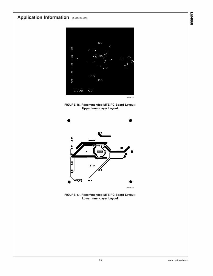
FIGURE 16. Recommended MTE PC Board Layout:Upper Inner-Layer Layout
20026773
FIGURE 17. Recommended MTE PC Board Layout:Lower Inner-Layer Layout
LM4868
www.national.com23
Application Information (Continued)
20026774
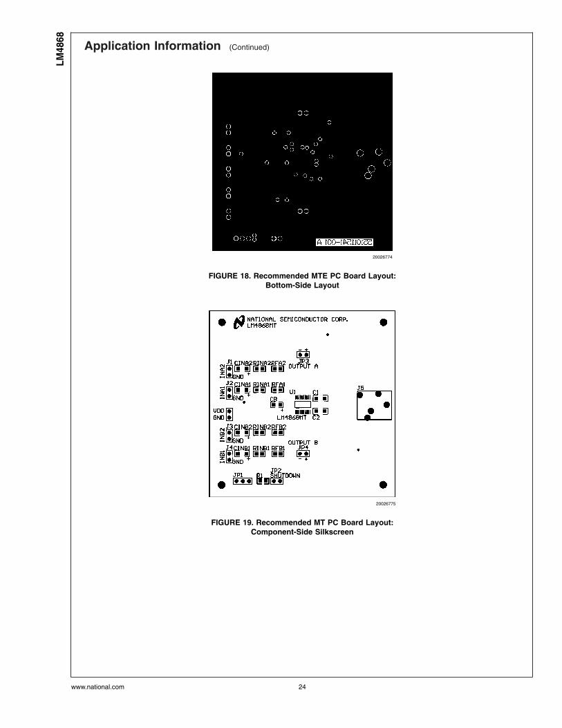
FIGURE 18. Recommended MTE PC Board Layout:Bottom-Side Layout
20026775
FIGURE 19. Recommended MT PC Board Layout:Component-Side Silkscreen
LM48
68
www.national.com 24
Application Information (Continued)
20026776
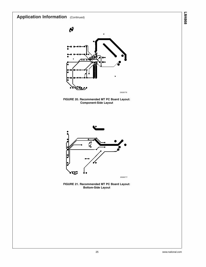
FIGURE 20. Recommended MT PC Board Layout:Component-Side Layout
20026777
FIGURE 21. Recommended MT PC Board Layout:Bottom-Side Layout
LM4868
www.national.com25
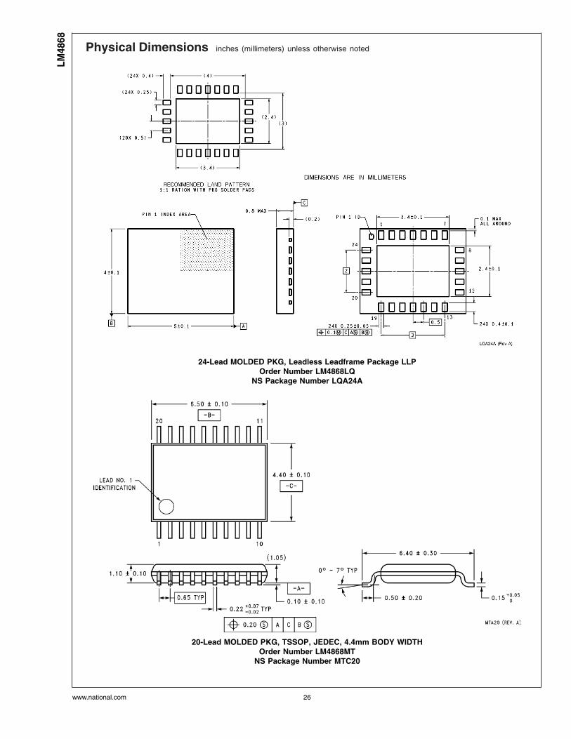
Physical Dimensions inches (millimeters) unless otherwise noted
24-Lead MOLDED PKG, Leadless Leadframe Package LLPOrder Number LM4868LQ
NS Package Number LQA24A
20-Lead MOLDED PKG, TSSOP, JEDEC, 4.4mm BODY WIDTHOrder Number LM4868MT
NS Package Number MTC20
LM48
68
www.national.com 26
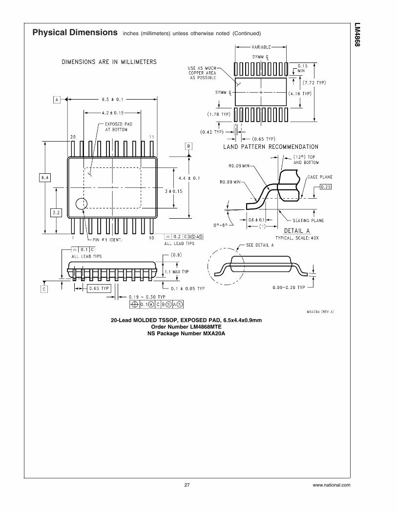
Physical Dimensions inches (millimeters) unless otherwise noted (Continued)
20-Lead MOLDED TSSOP, EXPOSED PAD, 6.5x4.4x0.9mmOrder Number LM4868MTE
NS Package Number MXA20A
LM4868
www.national.com27
Notes
LIFE SUPPORT POLICY
NATIONAL’S PRODUCTS ARE NOT AUTHORIZED FOR USE AS CRITICAL COMPONENTS IN LIFE SUPPORTDEVICES OR SYSTEMS WITHOUT THE EXPRESS WRITTEN APPROVAL OF THE PRESIDENT AND GENERALCOUNSEL OF NATIONAL SEMICONDUCTOR CORPORATION. As used herein:
1. Life support devices or systems are devices orsystems which, (a) are intended for surgical implantinto the body, or (b) support or sustain life, andwhose failure to perform when properly used inaccordance with instructions for use provided in thelabeling, can be reasonably expected to result in asignificant injury to the user.
2. A critical component is any component of a lifesupport device or system whose failure to performcan be reasonably expected to cause the failure ofthe life support device or system, or to affect itssafety or effectiveness.
National SemiconductorCorporationAmericasEmail: [email protected]
National SemiconductorEurope
Fax: +49 (0) 180-530 85 86Email: [email protected]
Deutsch Tel: +49 (0) 69 9508 6208English Tel: +44 (0) 870 24 0 2171Français Tel: +33 (0) 1 41 91 8790
National SemiconductorAsia Pacific CustomerResponse GroupTel: 65-2544466Fax: 65-2504466Email: [email protected]
National SemiconductorJapan Ltd.Tel: 81-3-5639-7560Fax: 81-3-5639-7507
www.national.com
LM48
68O
utpu
t-Tr
ansi
ent-
Free
Dua
l2.1
WA
udio
Am
plifi
erP
lus
No
Cou
plin
gC
apac
itor
Ste
reo
Hea
dpho
neFu
nctio
n
National does not assume any responsibility for use of any circuitry described, no circuit patent licenses are implied and National reserves the right at any time without notice to change said circuitry and specifications.