Radiation Tests of Semiconductor Detectors10452/... · 2006-06-20 · Valery Chmill: Radiation...
106
Radiation Tests of Semiconductor Detectors Valery Chmill KUNGL TEKNISKA H ¨ OGSKOLAN Fysiska Institutionen Stockholm 2006
Transcript of Radiation Tests of Semiconductor Detectors10452/... · 2006-06-20 · Valery Chmill: Radiation...
Radiation Tests of SemiconductorDetectors
Valery Chmill
KUNGL TEKNISKA HOGSKOLANFysiska Institutionen
Stockholm 2006

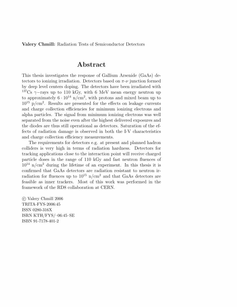
Valery Chmill: Radiation Tests of Semiconductor Detectors
Abstract
This thesis investigates the response of Gallium Arsenide (GaAs) de-tectors to ionizing irradiation. Detectors based on π-ν junction formedby deep level centers doping. The detectors have been irradiated with137Cs γ−rays up to 110 kGy, with 6 MeV mean energy neutron upto approximately 6 · 1014 n/cm2, with protons and mixed beam up to1015 p/cm2. Results are presented for the effects on leakage currentsand charge collection efficiencies for minimum ionizing electrons andalpha particles. The signal from minimum ionizing electrons was wellseparated from the noise even after the highest delivered exposures andthe diodes are thus still operational as detectors. Saturation of the ef-fects of radiation damage is observed in both the I-V characteristicsand charge collection efficiency measurements.
The requirements for detectors e.g. at present and planned hadroncolliders is very high in terms of radiation hardness. Detectors fortracking applications close to the interaction point will receive chargedparticle doses in the range of 110 kGy and fast neutron fluences of1014 n/cm2 during the lifetime of an experiment. In this thesis it isconfirmed that GaAs detectors are radiation resistant to neutron ir-radiation for fluences up to 1015 n/cm2 and that GaAs detectors arefeasible as inner trackers. Most of this work was performed in theframework of the RD8 collaboration at CERN.
c© Valery Chmill 2006TRITA-FYS-2006:45ISSN 0280-316XISRN KTH/FYS/–06:45–SEISBN 91-7178-401-2

Contents
1 Introduction 31.1 Background . . . . . . . . . . . . . . . . . . . . . . . . 31.2 Aims of Work . . . . . . . . . . . . . . . . . . . . . . . 41.3 Properties of Semiconductor . . . . . . . . . . . . . . . 51.4 Band Structure . . . . . . . . . . . . . . . . . . . . . . 51.5 Charge Carrier Mobility and Drift Velocity . . . . . . . 81.6 Classification of Defects in Semiconductor . . . . . . . 81.7 Author’s Contribution . . . . . . . . . . . . . . . . . . 10
1.7.1 List of publications included in thesis. . . . . . 111.7.2 List of publications not included in thesis. . . . 12
2 Description of Investigated Structures 142.1 Technology . . . . . . . . . . . . . . . . . . . . . . . . 15
2.1.1 Diffusion . . . . . . . . . . . . . . . . . . . . . . 152.1.2 Epitaxy . . . . . . . . . . . . . . . . . . . . . . 16
3 Response of GaAs detectors to Ionizing Irradiation 193.1 Measuring bench . . . . . . . . . . . . . . . . . . . . . 213.2 Response of the GaAs samples to radioactive sources . 223.3 Signal formation mechanism and estimations of charge
collection time . . . . . . . . . . . . . . . . . . . . . . . 253.4 Temperature dependence of the properties of π-ν struc-
tures . . . . . . . . . . . . . . . . . . . . . . . . . . . . 313.5 γ–ray irradiation of GaAs structures . . . . . . . . . . 34
4 Neutron Irradiation of GaAs Structures 374.1 Description of the experimental method . . . . . . . . 374.2 Irradiation induced defects and test structures properties 39
1
2 Contents
4.3 Sensitivity of GaAs structures to minimum ionizing betaparticles . . . . . . . . . . . . . . . . . . . . . . . . . . 44
4.4 Conclusion . . . . . . . . . . . . . . . . . . . . . . . . . 47
5 Irradiation in Mixed Beam at CERN 485.1 Introduction . . . . . . . . . . . . . . . . . . . . . . . . 485.2 Investigated structures . . . . . . . . . . . . . . . . . . 495.3 Experimental details . . . . . . . . . . . . . . . . . . . 505.4 Exposure in mixed beam, basic results . . . . . . . . . 515.5 Signal estimation . . . . . . . . . . . . . . . . . . . . . 56
6 Microstrip Detectors Test 576.1 Main parameters of the microstrip detectors . . . . . . 586.2 Experimental set-up . . . . . . . . . . . . . . . . . . . 606.3 The beam test results . . . . . . . . . . . . . . . . . . . 616.4 Investigation of radiation hardness . . . . . . . . . . . 65
7 GaAs detectors for α-particles and heavy ions spectrom-etry 687.1 Introduction . . . . . . . . . . . . . . . . . . . . . . . . 687.2 Detector manufacture technology . . . . . . . . . . . . 697.3 Electrical characteristics . . . . . . . . . . . . . . . . . 697.4 Detector performance for α-particles . . . . . . . . . . 72
8 X-ray Irradiation of Silicon Detectors 768.1 Experimental layout . . . . . . . . . . . . . . . . . . . 778.2 Results and discussions . . . . . . . . . . . . . . . . . . 798.3 Summary . . . . . . . . . . . . . . . . . . . . . . . . . 86
9 Summary and Outlook 879.1 Comparison with prediction from Local Charge Neutral-
ity model . . . . . . . . . . . . . . . . . . . . . . . . . 879.2 Rate of Irradiation . . . . . . . . . . . . . . . . . . . . 899.3 Conclusion . . . . . . . . . . . . . . . . . . . . . . . . . 90
10 Acknowledgments 92
Chapter 1
Introduction
1.1 Background
The operation of semiconductor detectors in harsh radiation environ-ments depends strongly on the radiation hardness of the device. Onesuch environment is the CERN Large Hadron Collider (LHC). Herethe inner tracker detectors close to the interaction point will receivecharged particle doses in the range of 110 kGy and fast neutron fluencesof 1014 n/cm2 during the lifetime of an experiment. Applications withharsh radiation environments exist in a wide range of fields from ex-periments with high charged particle multiplicity to proton and nucleiirradiation therapy. The basic damage mechanisms in semiconductorsare conveniently separated into two categories:
a) Bulk effects, which are manifestations of the displacement ofatoms from their normal sites in the crystal lattice.
b) Surface effects, which are long-term ionization effects in the in-sulators connected with the active semiconductor region.
Modern electronics is based on semiconductor structures formed bythe introduction of impurities into semiconductors, thus creating cen-ters with shallow energy levels (see later in this chapter). The SiberianInstitute of Technology in Tomsk, Russia, has over the last twenty yearsadopted a non-traditional approach to create device structures throughdoping semiconductors with impurities which create centers with deep
3
4 Chapter 1. Introduction
energy levels. The resulting, so called π-ν structures enabled new de-vices, since these structures allows to form high ohmical intrinsic-likeGaAs material.
In this thesis, the effects of bulk damage due to gamma, neutron,proton and pion irradiation on the properties of GaAs detectors interms of current as a function of voltage (I-V), capacitance as a func-tion of reverse bias voltage (C-V) measurements and charge collectionefficiency degradation are experimentally investigated.
The thesis also includes a study of recovery effects of a Si-detectorsby voltage training from X-ray irradiation.
1.2 Aims of Work
The aims of this work are to enhance the understanding of GaAs withdeep level dopants from an experimental physics point of view and tostudy the radiation hardness of GaAs for high energy physics applica-tions. More specifically this involved:
• investigation of differences between industry-standard, SI-U (Semi-Insulating, Undoped), LEC (Liquid-Encapsulated Czochralski [1])and epitaxially-grown GaAs layers
• provide input to optimize fabrication technology for simple padand microstrip detectors production
• evaluation of the radiation hardness of GaAs detectors to chargedparticles, neutrons and gamma
• testing of commercial and laboratory pad and microstrip detec-tors to LHC specification with LHC speed read-out electronics
• development of methods for enhancing the detection efficiency forionizing radiation.
• investigate the feasibility of GaAs detectors as α-particles spec-troscopy detectors
1.3. Properties of Semiconductor 5
1.3 Properties of Semiconductor
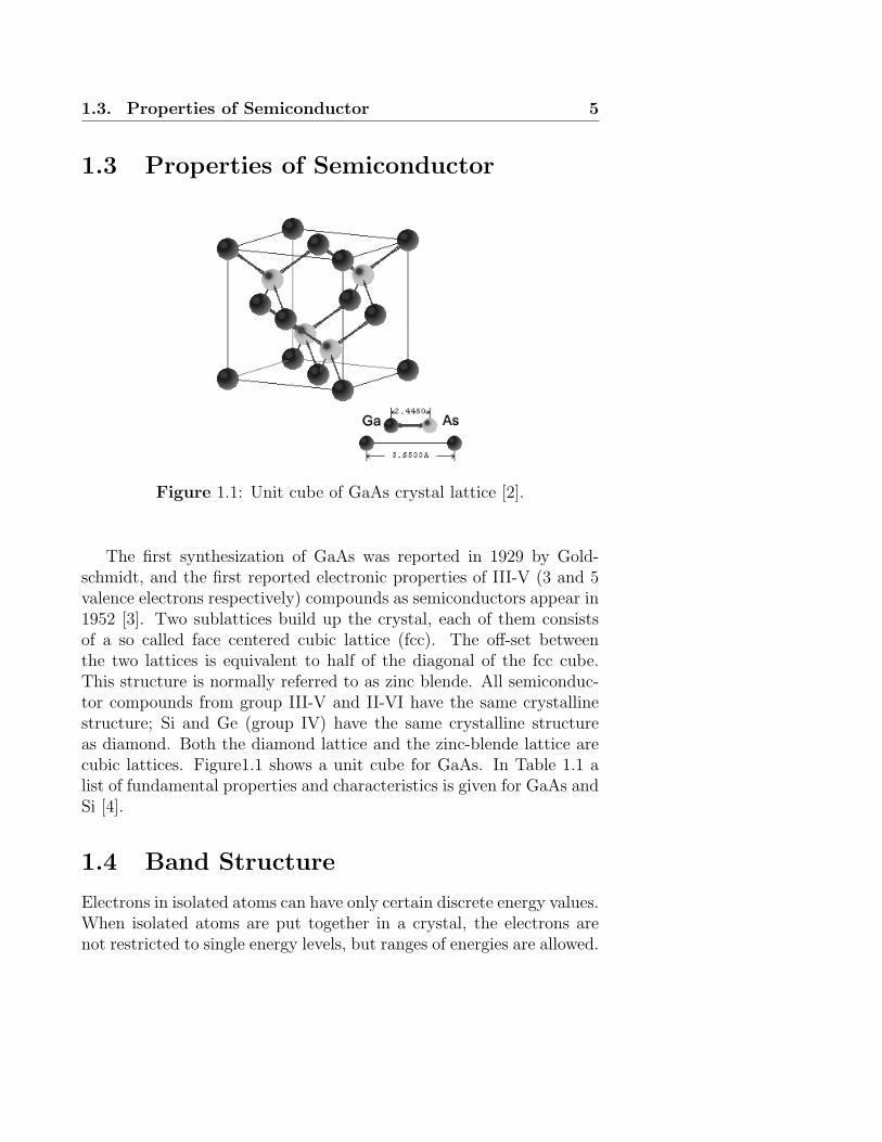
Figure 1.1: Unit cube of GaAs crystal lattice [2].
The first synthesization of GaAs was reported in 1929 by Gold-schmidt, and the first reported electronic properties of III-V (3 and 5valence electrons respectively) compounds as semiconductors appear in1952 [3]. Two sublattices build up the crystal, each of them consistsof a so called face centered cubic lattice (fcc). The off-set betweenthe two lattices is equivalent to half of the diagonal of the fcc cube.This structure is normally referred to as zinc blende. All semiconduc-tor compounds from group III-V and II-VI have the same crystallinestructure; Si and Ge (group IV) have the same crystalline structureas diamond. Both the diamond lattice and the zinc-blende lattice arecubic lattices. Figure1.1 shows a unit cube for GaAs. In Table 1.1 alist of fundamental properties and characteristics is given for GaAs andSi [4].
1.4 Band Structure
Electrons in isolated atoms can have only certain discrete energy values.When isolated atoms are put together in a crystal, the electrons arenot restricted to single energy levels, but ranges of energies are allowed.
6 Chapter 1. Introduction
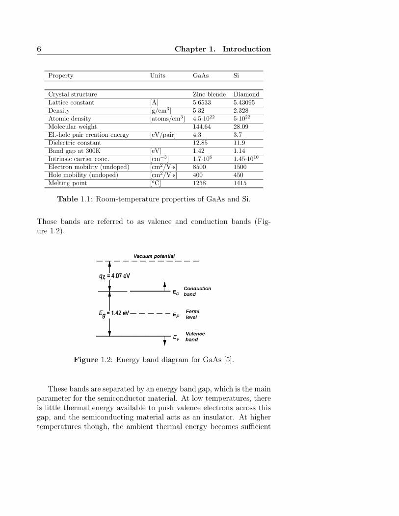
Property Units GaAs Si
Crystal structure Zinc blende DiamondLattice constant [A] 5.6533 5.43095Density [g/cm3] 5.32 2.328Atomic density [atoms/cm3] 4.5·1022 5·1022
Molecular weight 144.64 28.09El.-hole pair creation energy [eV/pair] 4.3 3.7Dielectric constant 12.85 11.9Band gap at 300K [eV] 1.42 1.14Intrinsic carrier conc. [cm−3] 1.7·106 1.45·1010
Electron mobility (undoped) [cm2/V·s] 8500 1500Hole mobility (undoped) [cm2/V·s] 400 450Melting point [oC] 1238 1415
Table 1.1: Room-temperature properties of GaAs and Si.
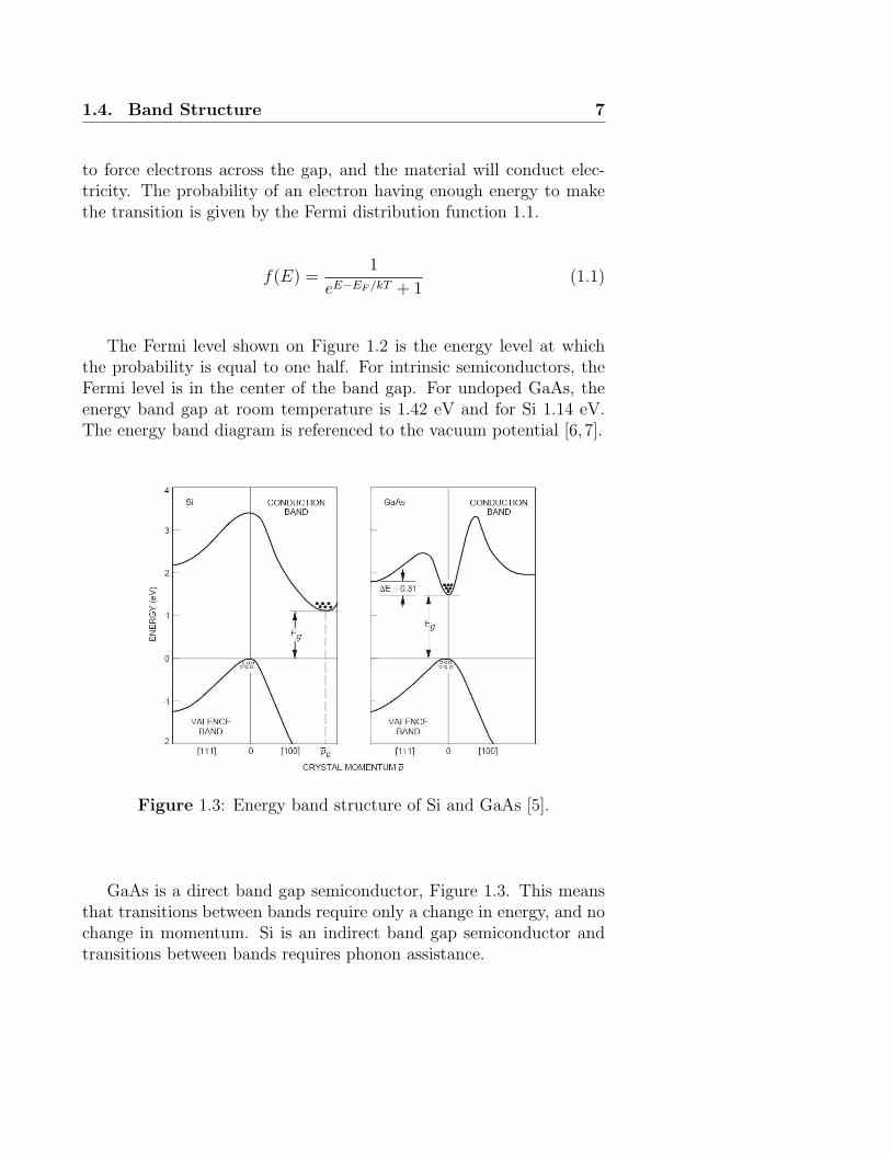
Those bands are referred to as valence and conduction bands (Fig-ure 1.2).
Figure 1.2: Energy band diagram for GaAs [5].
These bands are separated by an energy band gap, which is the mainparameter for the semiconductor material. At low temperatures, thereis little thermal energy available to push valence electrons across thisgap, and the semiconducting material acts as an insulator. At highertemperatures though, the ambient thermal energy becomes sufficient
1.4. Band Structure 7
to force electrons across the gap, and the material will conduct elec-tricity. The probability of an electron having enough energy to makethe transition is given by the Fermi distribution function 1.1.
f(E) =1
eE−EF /kT + 1(1.1)
The Fermi level shown on Figure 1.2 is the energy level at whichthe probability is equal to one half. For intrinsic semiconductors, theFermi level is in the center of the band gap. For undoped GaAs, theenergy band gap at room temperature is 1.42 eV and for Si 1.14 eV.The energy band diagram is referenced to the vacuum potential [6, 7].
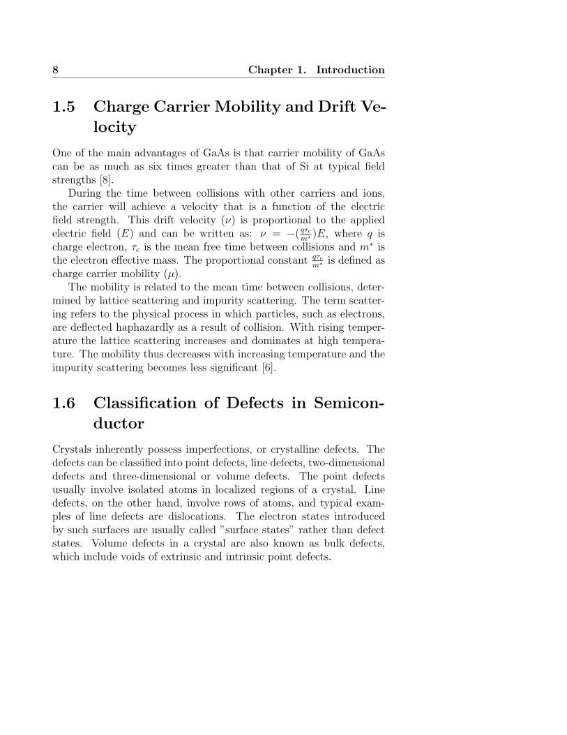
Figure 1.3: Energy band structure of Si and GaAs [5].
GaAs is a direct band gap semiconductor, Figure 1.3. This meansthat transitions between bands require only a change in energy, and nochange in momentum. Si is an indirect band gap semiconductor andtransitions between bands requires phonon assistance.
8 Chapter 1. Introduction
1.5 Charge Carrier Mobility and Drift Ve-
locity
One of the main advantages of GaAs is that carrier mobility of GaAscan be as much as six times greater than that of Si at typical fieldstrengths [8].
During the time between collisions with other carriers and ions,the carrier will achieve a velocity that is a function of the electricfield strength. This drift velocity (ν) is proportional to the appliedelectric field (E) and can be written as: ν = −( qτc
m∗ )E, where q ischarge electron, τc is the mean free time between collisions and m∗ isthe electron effective mass. The proportional constant qτc
m∗ is defined ascharge carrier mobility (µ).
The mobility is related to the mean time between collisions, deter-mined by lattice scattering and impurity scattering. The term scatter-ing refers to the physical process in which particles, such as electrons,are deflected haphazardly as a result of collision. With rising temper-ature the lattice scattering increases and dominates at high tempera-ture. The mobility thus decreases with increasing temperature and theimpurity scattering becomes less significant [6].
1.6 Classification of Defects in Semicon-
ductor
Crystals inherently possess imperfections, or crystalline defects. Thedefects can be classified into point defects, line defects, two-dimensionaldefects and three-dimensional or volume defects. The point defectsusually involve isolated atoms in localized regions of a crystal. Linedefects, on the other hand, involve rows of atoms, and typical exam-ples of line defects are dislocations. The electron states introducedby such surfaces are usually called ”surface states” rather than defectstates. Volume defects in a crystal are also known as bulk defects,which include voids of extrinsic and intrinsic point defects.
1.6. Classification of Defects in Semiconductor 9
The crystal point defects in semiconductor can be classified as fol-lows:
• Vacancy: created by a missing atom.
• Interstitial: atom occupying interstitial site (is located in a non-lattice site).
• Substitutional: impurity atom replacing the host atom.
• Antisite: a special kind of substitutional defect when a hostatom occupies the site of another host atom.
• Frenkel defect pair: a complex formed by the host atom dis-placed from a lattice site to a nearby interstitial site (vacancy-interstitial).
• Impurities: defects involving foreign atoms (i.e., impurities) arereferred to as extrinsic defects.
All the listed effects are so called point defects, which are impor-tant since they strongly impact the performance of any semiconductordevice. For example they determine the dark current as well as thebias voltage for any detector [9–11].
Intrinsic defects in GaAs include both arsenic and gallium vacancies.The effect of these vacancy defects has been observed to be neutral [12],deep donor-like, and deep acceptor-like [13]. A donor-like defect locatedat the middle of the energy band gap is the so called EL2 defect [14].This defect is important since it enables a conversion of p-type GaAsto semi-insulating. The EL2 defect is more frequent in material grownfrom an arsenic rich melt.
The electrical properties of the semiconductor will change depend-ing on the impurity. Figure 1.4 shows the energy band diagram ofGaAs with the impurity additions. The impurities will shift the Fermilevel from the center of the band towards these impurity levels.
Doping impurities e.g. Cu, Se are referred to as shallow level im-purities accordingly [15–17] and impurities with energies in the centerof the band gap e.g. Fe, Cr as deep level centers. Device performanceis degraded by deep impurities since the charge carrier lifetime will beshorter.
10 Chapter 1. Introduction
Figure 1.4: Energy band diagram of GaAs with impurities [5].
GaAs resistivity can be controlled by precision doping with a deep-level impurity like Fe, Cr that has a conductivity type opposite ton-type impurities or defects introduced during growth. The impor-tance of semi-insulating GaAs is that devices made of it by direct ionimplantation are self-isolating, so they become well suited for detectorfabrication.
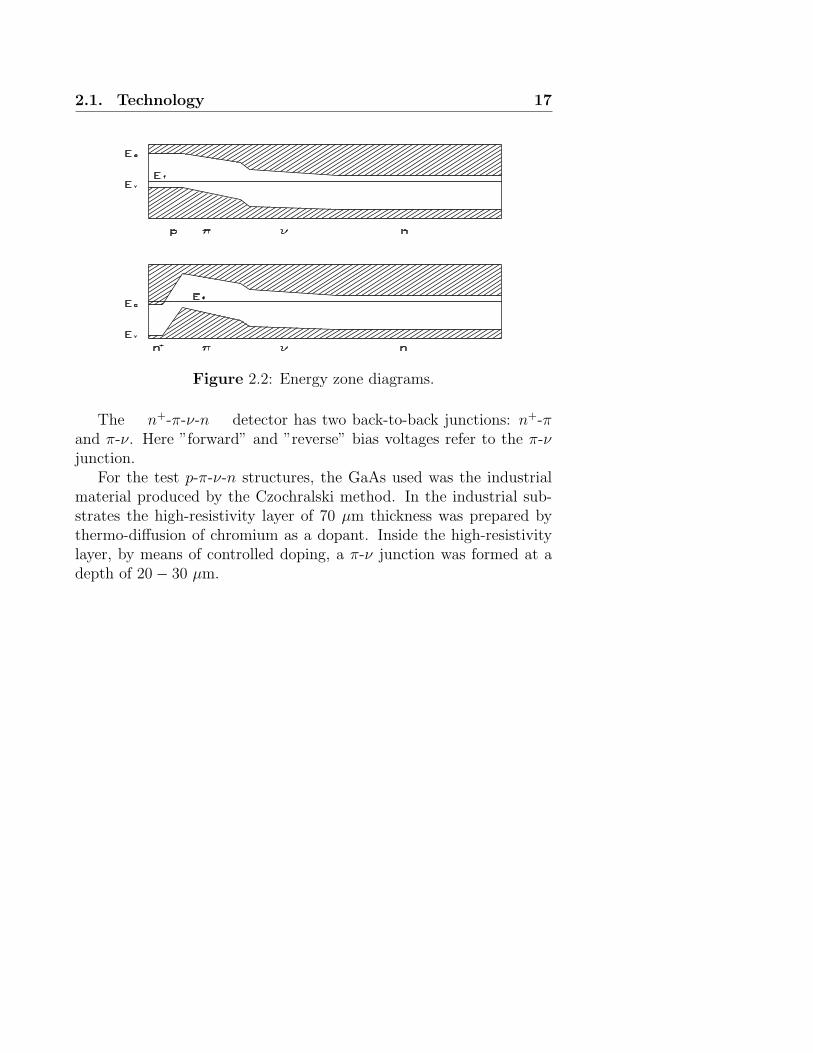
Tomsk GaAs researchers have entered the terms π-type and ν-typeconductivity layers in analogy with p−-type and n−-type to distinguishthe deep level centers doping from shallow level impurity doping. En-ergy zone diagrams of π-ν structures presented on Figure 2.2.
1.7 Author’s Contribution
The research presented in this thesis was performed at the Institute forHigh Energy Physics (Russia), at CERN (Switzerland) and at Kungl.Tekniska Hogskolan (Sweden) during the years 1993-2005. The thesisis based on work listed in Refs. [18–25].
For seven years I was heavily involved in the design and implemen-tation of beam tests of prototype Gallium Arsenide (GaAs) pad andmicrostrip detectors where the goal application was the inner detectorsof the ATLAS experiment at CERN, Geneva. This work was performedin the RD8 collaboration. I took a major part in the analysis of the
1.7. Author’s Contribution 11
data from these beam tests. Different combinations of detectors andelectronics were evaluated in parallel.
I was also involved in measurements on proposed front-end elec-tronics and in particular the optimization of the design of the pream-plifier. In this case the foreseen application was not only high energyphysics experiments like the ATLAS detector but also other imagingapplications. The electronics was of both hybrid types with discretecomponents mounted on a PCB and integrated analogue circuits with64 parallel channels.
The Siberian Physics Technical Institute in Tomsk has manufac-tured the GaAs detectors described in this thesis. This institute hasdeveloped a new technology for GaAs detector fabrication based ongrowing the GaAs crystal in a magnetic field resulting in an improvedcrystal with less defects. I have supplied this group with experimentalresults for optimizing the inner structure of the GaAs detectors.
I also evaluated the possibilities for the use of GaAs in the highintensity mixed beam employed by the CHORUS and NOMAD exper-iments at CERN [23].
In 1999-2001 I investigated possibilities of using GaAs detectorscompensated with deep level centers for alpha particle and heavy ionspectroscopy. The plan was that if the other requirements were ful-filled the detectors could, due to their radiation hardness, be used inenvironments where other materials would not work. The result waspromising as presented in [22] and the detectors may in the future beused in these applications.
I did a significant amount of the writing for articles [18–25] and wascorresponding author of all of them. If not explicitly stated otherwiseI performed all preparations for irradiation experiments and providedata collection and most of analysis myself.
1.7.1 List of publications included in thesis.
1. [18] Chmill V.B., Chuntonov A.V., Sergeev V.A., Smol A.V., TsyupaY.P., Vorobiev A.P., Gordienko A.I., Potapov A.I. An explorationof GaAs structures for solid state detectors. Nucl. Instr. andMeth., A326: pp.310-312, 1993.
2. [19] Chmill V.B., Chuntonov A.V., Smol A.V., Vorobiev A.P., Tol-
12 Chapter 1. Introduction
banov O.P., Koretskaya O.B. Exploration of GaAs structureswith π-ν junction for coordinate sensitive detectors. Nucl. Instr.and Meth., A340: pp.328-340, 1994.
3. [21] Chmill V.B., Chuntonov A.V., Krupnyi G.I. Rastsvetalov Ya.N.Radiation resistance of GaAs structures based on π-ν junctions.J.Phys. D: Appl. Phys. 28, , pp.559-564, 1995.
4. [20] Chmill V.B., Chuntonov A.V., Khludkov S.S., Smith K.M., Tol-banov O.P., Vorobiev A.P. Radiation hard microstrip detectorsbased on gallium arsenide. Nucl. Instr. and Meth., A379: pp.406-408, 1996.
5. [22] Chmill V.B., Chuntonov A.V., Falaleev V.V., Smith K.M., SmolA.V., Vorobiev A.P., Tolbanov O.P. The Result of GaAs Irra-diation at Mixed Beam Neutrino Cave CERN. Fifth Interna-tional Workshop on Gallium Arsenide Detectors and RelatedCompounds (Cividale del Friuli, Italy June17-20 1997) Nucl. In-str. and Meth., A410: pp.54-60, 1998.
6. [23] Chmill V.B., Chuntonov A.V., Smol A.V., Vorobiev A.P., Tol-banov O.P., Smith K.M. Particle detector based on GaAs. Radi-ation hardness and spatial resolution. Nucl. Instr. and Meth., A409: pp.247-250, 1998.
7. [24] Chmill V., Chuntonov A., Kholodenko A., Vorobiev A., TsyupaY., Porohovnichenko L., Potapov A., Klamra W. Investigationof epitaxial GaAs charged particle detectors. Nucl. Instr. andMeth., A438, pp.362-367, 1999.
8. [25] Chmill V. X-ray Irradiation of Silicon Detectors. Submitted toNucl. Instr. and Meth., 2006.
1.7.2 List of publications not included in thesis.
1. Chmill V.B., et al. Radiation Hard Microstrip Gallium ArsenideDetectors. Proceeding of the Third International Workshop onGallium Arsenide and Related Compounds. S.Miniato, Tuscany,Italy, March 21-24 1995. World Scientific Publishing Co Pte Ltd.
1.7. Author’s Contribution 13
2. M. Lundqvist, B. Cederstrom, V. Chmill, M. Danielsson and DNygren. Computer simulations and performance measurementson a silicon strip detector for edge-on imaging. IEEE Trans.Nucl. Science 47:(4), pp. 1487-1492, 2000.
3. M. Danielsson, H. Bornefalk, B. Cederstrom, V. Chmill, B. Hasegawa,M. Lundqvist, D. Nygren and T. Tabar, Dose-efficient system fordigital mammography, Proc SPIE Physics of Medical Imaging,3977, San Diego (2000)
4. Mats Lundqvist, Bjorn Cederstrom,Valery Chmill, Mats Daniels-son and Bruce Hasegawa, Evaluation of a Photon-Counting X-rayImaging System, IEEE Transactions on Nuclear Science, Vol 48(4) (2001)
5. M. Lundqvist, D. Bergstrom, B. Cederstrom, V. Chmill, A. Chuntonov,M. Danielsson and M. Aslund, Physical Evaluation of a Prototypefor the Sectra Microdose Mammography System, Proceedings 6thInternationa Workshop on Digital Mammography IWDM2002,Bremen, 2002, ed. Heinz-Otto Peitgen
6. Danielsson M, Cederstroem B, Chmill V, Lundqvist M, AslundM. Measurements on a full-field digital mammography systemwith a photon counting crystalline silicon detector. SPIE Phys.Med. Imaging 2003; 5030:547-552.
7. R.A. Achmadullin, V.V. Artemov, V.F. Dvoryankin, G.G. Dvoryank-ina, Yu.M. Dikaev, M.G. Ermakov, O.N. Ermakova, V.B. Chmil,A.G. Holodenko, A.A. Kudryashov, A.I. Krikunov, A.G. Petrov,A.A. Telegin and A.P. Vorobiev. Photovoltaic x-ray detectorsbased on epitaxial GaAs structures. Nucl. Instr. and Meth.,A554, pp.314-319, 2005.
Chapter 2
Description of InvestigatedStructures
A microstrip semiconductor detector has to contain a high-resistivitylayer. In case of Si, depleted by external bias voltage, a p–n structurewith an impurity concentration of 1011–1013 cm−3 has been taken as thebasis. GaAs can not be grown as pure as Si, at least not yet, and theTomsk engineers have chosen another way of making the concentrationsof donors and acceptors equal to each other – compensated GaAs. Thischoice has substantiated the high radiation hardness.
For the test structures, the GaAs detectors were fabricated bothfrom laboratory material and from industrial material. The GaAs wasgrown in a magnetic field by the Bridgeman [26] method in the SiberianInstitute for Physics and Technology, Tomsk (basically a controlledfreezing process taking place under liquid - solid equilibrium condi-tions). The industrial material was produced following the Czochral-ski [1] method (the crystal is pulled from the melt). We have low-resistivity n–type GaAs in industrial case and high-resistivity for lab-oratory material.
14
2.1. Technology 15
2.1 Technology
There are two technologies used by the Tomsk group to form high-resistivity layers: diffusion and epitaxy.
2.1.1 Diffusion
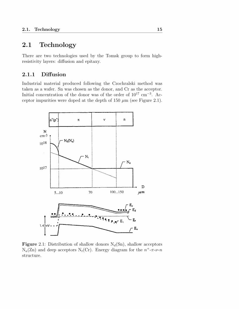
Industrial material produced following the Czochralski method wastaken as a wafer. Sn was chosen as the donor, and Cr as the acceptor.Initial concentration of the donor was of the order of 1017 cm−3. Ac-ceptor impurities were doped at the depth of 150 µm (see Figure 2.1).
Figure 2.1: Distribution of shallow donors Nd(Sn), shallow acceptorsNa(Zn) and deep acceptors Nt(Cr). Energy diagram for the n+-π-ν-nstructure.
16 Chapter 2. Description of Investigated Structures
Cr accepts electrons from Sn, otherwise, the acceptor compensates thedonor, thus, the high-resistivity region of 109 Ohm·cm is formed at adepth of 70 µm (full thickness of sensitive layer ∼100–150 µm). Thatstructure has been named as p-π-ν-n. The π-layer is weak p-type andthe ν- one is weak n-type. Both layers can be considered as pseudo-intrinsic. Advantages:
large surface area – up to 5 inch in diameter.
Disadvantage:
chromium solubility, as well thickness of sensitive layer are lim-ited: 150 µm at 1017 cm−3 impurity.
2.1.2 Epitaxy
Advantages:
resistivity distribution of sensitive region is even.
Disadvantage:
very small surface area can be made – no more than 10 mm2.
Two main structure types were investigated: p-π-ν-n and n+-π-ν-n.The contact layer was made of either n+– or p– type GaAs.
On the n-type substrate the high-resistivity layer was grown byliquid-phase epitaxy with Fe as a dopant. The layer thickness wasabout ∼150 µm and the resistivity 107 Ohm·cm.
The dopant concentration gradient, specified during the doping pro-cess in the π– and ν– regions induces an internal electrical field. In astructure without an applied biasing field, the average strength of theelectrical field is 350 V/m, whereas in the space charge region (SCR)of the π-ν junction it can reach 104 V/m.
The energy zone diagrams for the samples are given in Figure 2.2.
2.1. Technology 17
Figure 2.2: Energy zone diagrams.
The n+-π-ν-n detector has two back-to-back junctions: n+-πand π-ν. Here ”forward” and ”reverse” bias voltages refer to the π-νjunction.
For the test p-π-ν-n structures, the GaAs used was the industrialmaterial produced by the Czochralski method. In the industrial sub-strates the high-resistivity layer of 70 µm thickness was prepared bythermo-diffusion of chromium as a dopant. Inside the high-resistivitylayer, by means of controlled doping, a π-ν junction was formed at adepth of 20− 30 µm.
18 Chapter 2. Description of Investigated Structures
Bridgeman CzochralskiEpitaxy Thermo-diffusion
T n+, pγ n+, pn p(Fe) p(Cr)p n+(Cr)mix p(Cr)strip n+(Cr)α p+(pure)
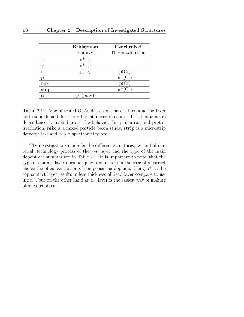
Table 2.1: Type of tested GaAs detectors, material, conducting layerand main dopant for the different measurements. T is temperaturedependance, γ, n and p are the behavior for γ, neutron and protonirradiation, mix is a mixed particle beam study, strip is a microstripdetector test and α is a spectrometry test.
The investigations made for the different structures, i.e. initial ma-terial, technology process of the π-ν layer and the type of the maindopant are summarized in Table 2.1. It is important to note, that thetype of contact layer does not play a main role in the case of a correctchoice the of concentration of compensating dopants. Using p+ as thetop contact layer results in less thickness of dead layer compare to us-ing n+, but on the other hand an n+ layer is the easiest way of makingohmical contact.
Chapter 3
Response of GaAs detectorsto Ionizing Irradiation
The investigated samples were plates of n–type GaAs with surface areavarying from 2×2 to 5×10 mm2 and 200−300 µm thickness. By meansof thermo-diffusion or epitaxy, either gas-phase or liquid-phase, a high-resistivity 100 ± 50 µm thick layer with resistivity 105 − 107 Ohm·cmhas been formed on these plates. Inside this layer, through controlleddoping with iron group elements, a π-ν junction which penetrates 70±20 µm into the layer is formed. The dopant concentration gradient,specified during the doping process in those π– and ν– regions inducedan internal electrical field.
19
20Chapter 3. Response of GaAs detectors to Ionizing
Irradiation
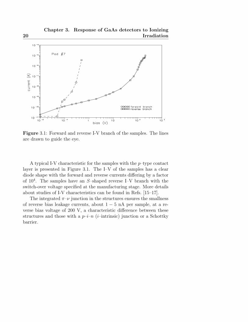
Figure 3.1: Forward and reverse I-V branch of the samples. The linesare drawn to guide the eye.
A typical I-V characteristic for the samples with the p–type contactlayer is presented in Figure 3.1. The I–V of the samples has a cleardiode shape with the forward and reverse currents differing by a factorof 104. The samples have an S–shaped reverse I–V branch with theswitch-over voltage specified at the manufacturing stage. More detailsabout studies of I-V characteristics can be found in Refs. [15–17].
The integrated π–ν junction in the structures ensures the smallnessof reverse bias leakage currents, about 1 − 5 nA per sample, at a re-verse bias voltage of 200 V, a characteristic difference between thesestructures and those with a p–i–n (i–intrinsic) junction or a Schottkybarrier.
3.1. Measuring bench 21
3.1 Measuring bench
The characteristics of GaAs structures were investigated by means ofa measuring bench with two independent electronic channels:
Channel one — a charge sensitive amplifier; an amplifier-shaperwith an active filter Polon 1101 (Ortec) and a self-triggered peak sen-sitive pulse analog-digital converter (ADC) ADC 712 . The calibrationof the channel is approximately:
Q(N) = 230 ·N + 250 [e−], (3.1)
where Q is the charge in electrons collected at the input of the amplifier,and N is the ADC channel number . The optimum Gaussian shapingtime for the output signal ts = 1 µs, was chosen such as to minimizethe noise in the channel. At an equivalent detector capacity the noiseat the input of the amplifier is approximately 1600 electrons (FWHM).
Channel two — a current sensitive amplifier ”Garantiya” [27],a ”strobable integrator” analog-digital converter LeCROY 2249A andtrigger electronics. The gate length required to trigger the ADC was40 ns. The equivalent noise charge at the input of the amplifier was3500 electrons (FWHM). The calibration of the channel is approxi-mated by:
Q(N) = 400 ·N + 4100 [e−], (3.2)
All the electronics except the trigger system is industrial and madein CAMAC standard. The information was read out by a standardcomputer through a CAMAC crate controller.
22Chapter 3. Response of GaAs detectors to Ionizing
Irradiation
3.2 Response of the GaAs samples to ra-
dioactive sources
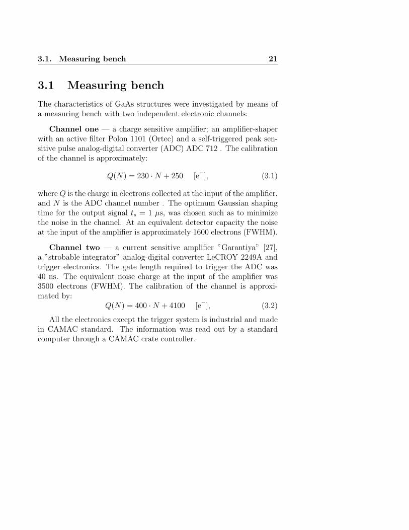
As a result of the repeated investigations of different structures withdoping of the active layers by dopants with deep levels (Fe, Cr), n+-π-ν-n and p-π-ν-n structures have shown the best signal to noise ratiosand the highest charge collection efficiency. Figure 3.2 shows the chargespectra of the signals from a radioactive 106Ru β–source, (3.55 MeVend-point energy) obtained with the p-π-ν-n structure using the chargesensitive channel.
Figure 3.2: Spectra of the signals from p-π-ν-n structure registered inthe charge sensitive channel for different bias voltage.
The signal due to the β–particles can be clearly detected above thenoise peak even at zero bias. Clearly, the bias voltage of a sample doesnot affect the charge collection efficiency. This shows that the SpaceCharge Region (SCR), as well as the regions of π– and ν– layers, arefully depleted by the intrinsic electric field. Another indication of thisfact is the weak dependence of the structure capacitance on the reversebias voltage, see Figure 3.3.
3.2. Response of the GaAs samples to radioactive sources23
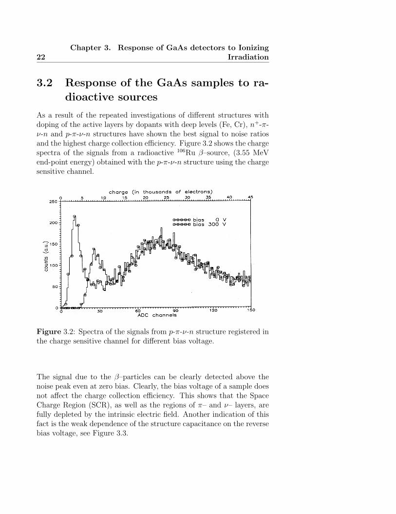
Figure 3.3: C–V of the p-π-ν-n sample (at the frequency 1 MHz).
Figure 3.4: Spectrum of the signals from the n+-π-ν-n structure, ex-posed to 2 MeV β–particles, registered in the charge sensitive channel;the full line represents the fitted Landau distribution for the ionizationlosses in the thin layer.
The response of n+-π-ν-n structures to monoenergetic β–particles withenergies between 0.6 MeV and 3.1 MeV was explored in detail in
24Chapter 3. Response of GaAs detectors to Ionizing
Irradiation
Ref. [28]. Of greatest interest are the experimental results of the ex-posure of samples to 2 MeV electrons ( minimum ionizing particles)for which the energy loss can be approximated by the Landau distri-bution [29] for ionization losses in a thin layer of matter. Such a dis-tribution in the 150 µm thick n+-π-ν-n high-resistivity sensitive layeris illustrated Figure 3.4.
For minimum ionizing particles, the most probable ionizing energyloss in GaAs is 6.48 MeV/cm. The generation of an electron–holepair requires on average 4.2 eV. Therefore, 23000 pairs are expectedin the 150 µm layer of the sample active region. From Figure 3.4, themost probable value of the collected charge is 22000 electrons, whichcorresponds to a charge collection efficiency of more than 95%.
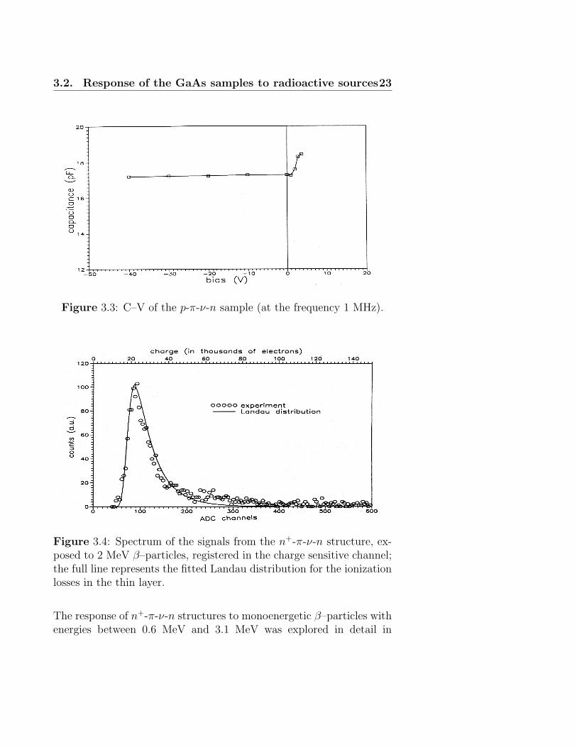
Figure 3.5: Spectrum of the signals from the n+-π-ν-n sample ex-posed to radioactive 241Am α–particles, registered in the charge sensi-tive channel.
Conventionally, the charge collection efficiency in Si and Ge detectorsis estimated from α–particle radiation. However, the high density ofcharge released at a depth of 5 − 10 µm from 5 MeV α–particles inGaAs results in a high density of pairs of charge carriers and, as aconsequence, in noticeable recombination. For this reason the chargecollection efficiency is not more than 20% in this case (Figure 3.5).
3.3. Signal formation mechanism and estimations of chargecollection time 25
In particular samples the thickness of the upper contact layer exceeds25 µm which is enough to stop α–particles. Nevertheless, we havedetected signals due to the ionization by α–particles.
Figure 3.5 shows the spectrum of the signals from 241Am α–particles(5.5 MeV) due to the ionization of the n+-π-ν-n structure.
3.3 Signal formation mechanism and esti-
mations of charge collection time
The model of the signal formation mechanism [28] in the semiconductorstructures is based on the following assumptions:
• the problem is one dimensional;
• the electric field in the sample should be constant;
• the track ionization density should not change;
• effects due to diffusion and charge carrier capture are negligible;
• no plasma effects are observed;
• the currents of electrons and holes are uncorrelated.
Then the problem is reduced to the motion of the charge columnin the fully depleted layer of the p-i-n structure. If the proper fieldstrength in the structure is 350 V/m, then the charge collection time,calculated by the drift model, should not exceed 500 ns. However, inanalysis of the response of the structures to β–particles some signalswere longer that 800 ns, whereas with 241Am α–particles the chargecollection period increased to even 1 µs, which exceeds the estimateobtained with the drift model.
To explain this effect, a plasma model has been applied whose es-sential points are: in the sensitive layer a charged particle (electron,in our case) leads to a high density of electron-hole pairs ∼ 1017cm−3.For the track diameter one may choose 0.5 µm, which is of the order ofmagnitude of the maximum δ–electron path length. For a track ioniza-tion density of 177 pairs/µm the necessary condition for the existenceof a plasma in a semiconductor should then be fulfilled [30], since at
26Chapter 3. Response of GaAs detectors to Ionizing
Irradiation
the given concentration of carriers the penetration depth of the internalelectrical field of the structure into the plasma is small compared to thelength of the plasma track. Clearly, the duration of the signal from thestructure will be extended by the plasma lifetime, tpl. In other words, itwill become longer by the time period starting when a particle enters adetector until the plasma state has decayed and all the carriers start tomove under the action of the electrical field. To estimate the time tpl,a model has been chosen [31] which exploits the ambipolar character ofdiffusion. Underlying the model were the assumptions that a particletrack has a cylindrical geometry and that in their motion away fromthe track the current carriers generate a current limited by the spacecharge.
tpl =
(3QoqenlA
32π3µ(εεo)2D2a
) 13
· 1
E; where, (3.3)
Qo — means the charge due to ionization,qe — is the elementary electrical charge;nl — is the linear density of the generated charge;µ — is the mobility of carriers;εεo — are the dielectric constant;Da — the ambipolar diffusion coefficient;A — the initial cross-sectional area of the track;E — the electrical field strength.
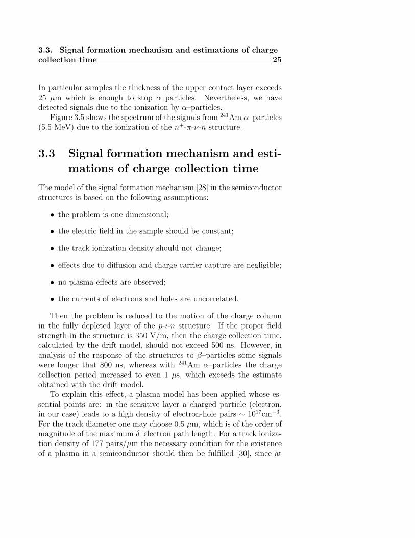
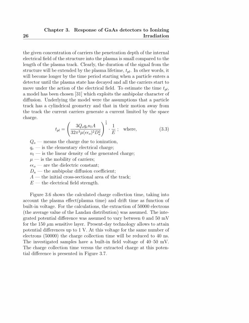
Figure 3.6 shows the calculated charge collection time, taking intoaccount the plasma effect(plasma time) and drift time as function ofbuilt-in voltage. For the calculations, the extraction of 50000 electrons(the average value of the Landau distribution) was assumed. The inte-grated potential difference was assumed to vary between 0 and 50 mVfor the 150 µm sensitive layer. Present-day technology allows to attainpotential differences up to 1 V. At this voltage for the same number ofelectrons (50000) the charge collection time will be reduced to 40 ns.The investigated samples have a built-in field voltage of 40–50 mV.The charge collection time versus the extracted charge at this poten-tial difference is presented in Figure 3.7.
3.3. Signal formation mechanism and estimations of chargecollection time 27
Figure 3.6: Estimated dependence of the charge collection time takinginto account the plasma effect for the release of 50000 electrons. Thelines are drawn by interpolating spline.
Figure 3.7: Estimated dependence of the charge collection time takinginto account the plasma effect at the integrated potential difference50 mV as function of the numbers of injected electron. The lines aredrawn by interpolating spline.
28Chapter 3. Response of GaAs detectors to Ionizing
Irradiation
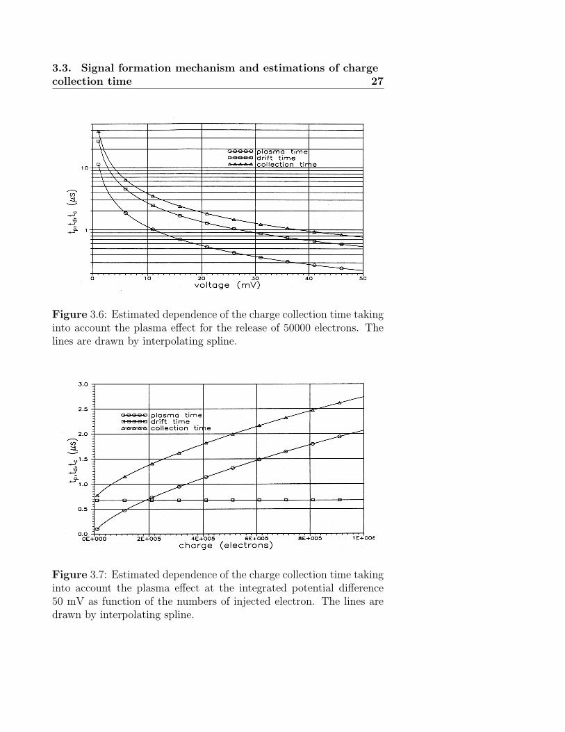
To get an experimental verification of the increase in the charge col-lection time (> 500 ns) due to the plasma lifetime in the structures,the samples were exposed to monoenergetic 2 MeV and 0.6 MeVβ–particles at different bias voltages. To get monoenergetic electronsfrom the radioactive source, a setup based on a permanent magnet wasused, described schematically in [28]. In experiments with monoener-getic beams, a 5× 10 mm2 sample of the p–π–ν–n structure was usedhaving a p–type contact layer in the form of a lattice.
Figure 3.8: The charge spectra of the signals from the p-π-ν-n sampleexposed to monoenergetic 0.6 MeV β–particles at various bias voltages.Every fifth data point is labelled. The lines drawn connecting everydata point.
Figure 3.8 shows the spectra of the signals obtained after exposure ofthe sample to 0.6 MeV monoenergetic electrons at bias voltages be-tween 0 and 300 V. The exposure to 0.6 MeV electrons is characterizedby multiple scattering in the 150 µm thick sensitive region. The signalcharge spectrum of these particles do not follow the Landau distribu-tion for ionization losses in a thin layer because of the accompanyingevents with a large number of extracted charge carriers. The shape ofthe distribution is practically unaltered at bias voltages above 100 V.
3.3. Signal formation mechanism and estimations of chargecollection time 29
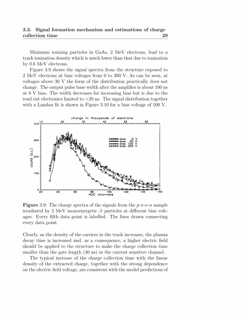
Minimum ionizing particles in GaAs, 2 MeV electrons, lead to atrack ionization density which is much lower than that due to ionizationby 0.6 MeV electrons.
Figure 3.9 shows the signal spectra from the structure exposed to2 MeV electrons at bias voltages from 0 to 300 V. As can be seen, atvoltages above 30 V the form of the distribution practically does notchange. The output pulse base width after the amplifier is about 100 nsat 0 V bias. The width decreases for increasing bias but is due to theread out electronics limited to >20 ns. The signal distribution togetherwith a Landau fit is shown in Figure 3.10 for a bias voltage of 100 V.
Figure 3.9: The charge spectra of the signals from the p-π-ν-n sampleirradiated by 2 MeV monoenergetic β–particles at different bias volt-ages. Every fifth data point is labelled. The lines drawn connectingevery data point.
Clearly, as the density of the carriers in the track increases, the plasmadecay time is increased and, as a consequence, a higher electric fieldshould be applied to the structure to make the charge collection timesmaller than the gate length (40 ns) in the current sensitive channel.
The typical increase of the charge collection time with the lineardensity of the extracted charge, together with the strong dependenceon the electric field voltage, are consistent with the model predictions of
30Chapter 3. Response of GaAs detectors to Ionizing
Irradiation
the influence of the plasma on the charge collection time. Calculationswhich take into account only the carrier drift in the depleted detectorregion surely underestimate the charge collection time.
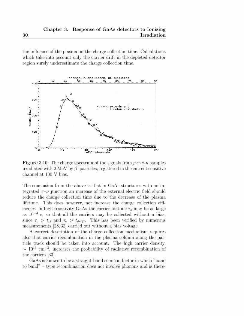
Figure 3.10: The charge spectrum of the signals from p-π-ν-n samplesirradiated with 2 MeV by β–particles, registered in the current sensitivechannel at 100 V bias.
The conclusion from the above is that in GaAs structures with an in-tegrated π–ν junction an increase of the external electric field shouldreduce the charge collection time due to the decrease of the plasmalifetime. This does however, not increase the charge collection effi-ciency. In high-resistivity GaAs the carrier lifetime τo may be as largeas 10−4 s, so that all the carriers may be collected without a bias,since τo > tpl and τo > tdrift. This has been verified by numerousmeasurements [28,32] carried out without a bias voltage.
A correct description of the charge collection mechanism requiresalso that carrier recombination in the plasma column along the par-ticle track should be taken into account. The high carrier density,∼ 1015 cm−3, increases the probability of radiative recombination ofthe carriers [33].
GaAs is known to be a straight-band semiconductor in which ”bandto band” – type recombination does not involve phonons and is there-

3.4. Temperature dependence of the properties of π-νstructures 31
fore accompanied by the emission of light quanta. The radiative re-combination lifetime, estimated in the Van Roosbroek and Schoklyemodel [34], was τr < 10−9 s, whereas estimates for the nonradioac-tive recombination lifetime gave τo ∼ 10−8 s. The recombination in thetrack channel should lead to spontaneous reradiation with hν ≤ Eq (Eq
being the band gap width). If, as supposed in [28], radiation due torecombination were selectively absorbed in the π–ν junction, then thenewly produced pairs would appear away from the track of the particle,which, in turn, would lower the density of nonequilibrium carriers inthe track. As a result this mechanism, together with the electric fieldand diffusion, would reduce the plasma lifetime. Presumably, however,due to the sharp increase of the optical absorption coefficient in thestrong electric field region (the Franz–Keldysh effect) [35] the radiationis absorbed selectively in the ambipolar diffusion field region inside theplasma column, generating new electron-hole pairs. This mechanismof charge transfer due to photoelectron transformations in GaAs maybe observed for samples with surface contact layer thicker than 20 µmwhere the α–particle stops (see Figure 3.5).
At a bias voltage of 100 V, the signal duration from these structureswas shorter than 20 ns (limited by the capability of the electronics).It follows from the above that structures with p–type GaAs strips maybe utilized as coordinate detectors in high luminosity experiments.
For the case of irradiation by 2 MeV β–particles (minimum ionizingparticles) the signal-to-noise ratio was equal to 8.5, while the detectionefficiency approached 100% for a threshold of the trigger electronics at3σ (noise).
Structures with an n+–type contact layer may be used for detectorsin experiments with relatively low luminosity, since such structureshave charge collection times between 150 and 1000 ns depending onthe extracted charge value. In this case an external electric field canhelp to reduce the charge collection time.
3.4 Temperature dependence of the prop-
erties of π-ν structures
To optimize the characteristics of semiconductor detectors in the oper-ating temperature range 10 to 70 oC, the process parameters at the
32Chapter 3. Response of GaAs detectors to Ionizing
Irradiation
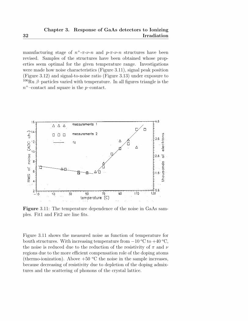
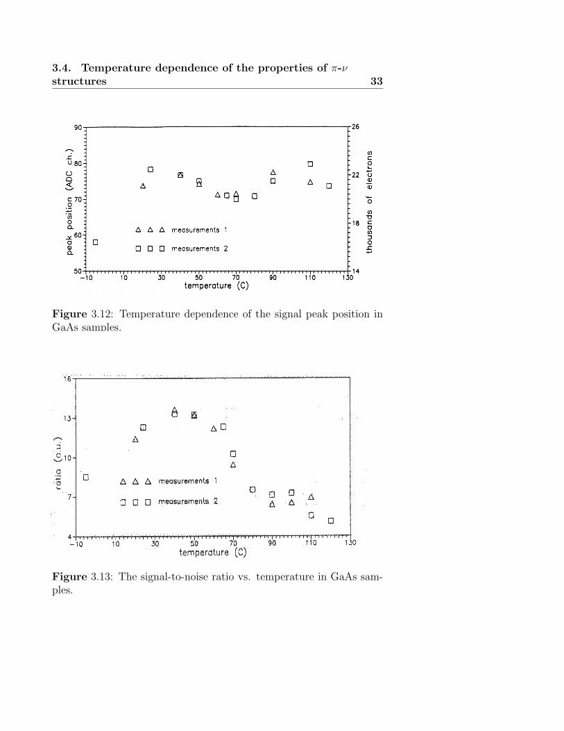
manufacturing stage of n+-π-ν-n and p-π-ν-n structures have beenrevised. Samples of the structures have been obtained whose prop-erties seem optimal for the given temperature range. Investigationswere made how noise characteristics (Figure 3.11), signal peak position(Figure 3.12) and signal-to-noise ratio (Figure 3.13) under exposure to106Ru β–particles varied with temperature. In all figures triangle is then+–contact and square is the p–contact.
Figure 3.11: The temperature dependence of the noise in GaAs sam-ples. Fit1 and Fit2 are line fits.
Figure 3.11 shows the measured noise as function of temperature forbouth structures. With increasing temperature from−10 oC to +40 oC,the noise is reduced due to the reduction of the resistivity of π and νregions due to the more efficient compensation role of the doping atoms(thermo-ionization). Above +50 oC the noise in the sample increases,because decreasing of resistivity due to depletion of the doping admix-tures and the scattering of phonons of the crystal lattice.
3.4. Temperature dependence of the properties of π-νstructures 33
Figure 3.12: Temperature dependence of the signal peak position inGaAs samples.
Figure 3.13: The signal-to-noise ratio vs. temperature in GaAs sam-ples.
34Chapter 3. Response of GaAs detectors to Ionizing
Irradiation
The location of the minimum noise value relative to the temperatureaxis can be optimized by varying the compensating admixture concen-tration, so that the signal-to-noise ratio is maximized in the operatingtemperature range (Figure 3.13).
3.5 γ–ray irradiation of GaAs structures
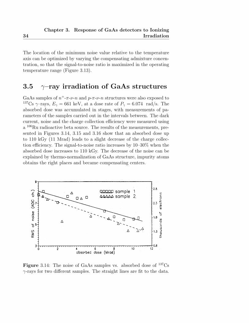
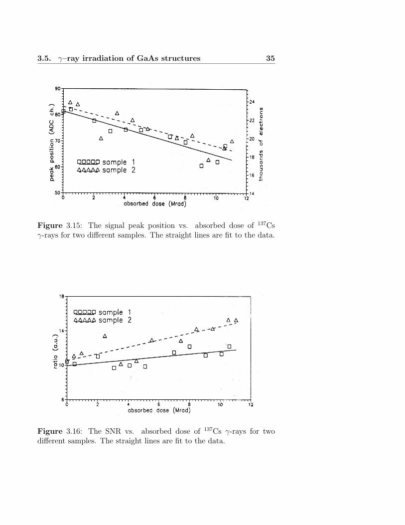
GaAs samples of n+-π-ν-n and p-π-ν-n structures were also exposed to137Cs γ–rays, Eγ = 661 keV, at a dose rate of Pγ = 6.074 rad/s. Theabsorbed dose was accumulated in stages, with measurements of pa-rameters of the samples carried out in the intervals between. The darkcurrent, noise and the charge collection efficiency were measured usinga 106Ru radioactive beta source. The results of the measurements, pre-sented in Figures 3.14, 3.15 and 3.16 show that an absorbed dose upto 110 kGy (11 Mrad) leads to a slight decrease of the charge collec-tion efficiency. The signal-to-noise ratio increases by 10–30% when theabsorbed dose increases to 110 kGy. The decrease of the noise can beexplained by thermo-normalization of GaAs structure, impurity atomsobtains the right places and became compensating centers.
Figure 3.14: The noise of GaAs samples vs. absorbed dose of 137Csγ-rays for two different samples. The straight lines are fit to the data.
3.5. γ–ray irradiation of GaAs structures 35
Figure 3.15: The signal peak position vs. absorbed dose of 137Csγ-rays for two different samples. The straight lines are fit to the data.
Figure 3.16: The SNR vs. absorbed dose of 137Cs γ-rays for twodifferent samples. The straight lines are fit to the data.
36Chapter 3. Response of GaAs detectors to Ionizing
Irradiation
Conclusion
The high charge collection efficiency (> 95%) that is independent ofthe external bias voltage, by virtue of the complete depletion of high-resistivity sensitive layers, may be achieved due to the high level ofcompensation in the starting material and the presence of an internalelectric field. Low-level noise is also attainable at a bias voltage due toS–shaped reverse I–V branch of the π-ν junction. These characteristicsgive detectors based on of p-π-ν-n structures significant advantage com-pared with available detector prototypes based on the p-i-n junctionsand Schottky barriers using semi-insulating GaAs [36–39].
The studies of the radiation resistance of the samples have revealedthat for a gamma dose of 110 kGy only a very minor deterioration isobserved.
The research into the mechanisms of charge collection and pulseformation processes allow to conclude that at external bias voltagesabove 100 V the charge collection time is independent of the extractedcharge value and that the pulse length in that case does not exceed afew nanoseconds.
It is important to note that detectors based on p-π-ν-n and n+-π-ν-n structures might operate, in principle, without an external biasvoltage under the action of only the internal electric field. In this casehowever, one should keep in mind the dependence of the pulse lengthon the created charge value.
Chapter 4
Neutron Irradiation of GaAsStructures
Introduction
In this chapter the results of experimental investigations of the effect ofvery large neutron fluences 1015 n/cm2 on the characteristics of GaAsdetector structures with π-ν – junctions are presented. The sensitiv-ity of this type of structure to ionizing radiation was described in theprevious chapter. The degradation of the GaAs structures is measuredin terms of the reduction in charge collection efficiency and signal tonoise ratio measured for minimum ionizing beta particles from a ra-dioactive 106Ru source and from changes in I–V and C–V electricalcharacteristics.
4.1 Description of the experimental method
The p-π-ν-n structures used in this test was fabricated from the Bridge-man method of crystal growth in a magnetic field and from the indus-trial GaAs material produced following the Czochralski method.
On Bridgeman material, a high-resistivity 107 Ohm·cm ∼ 150 µmthick layer was grown by epitaxy method with iron doping.
In the case of industrial substrates the high-resistivity layer of 70 µmthick was prepared by in-diffusion of chromium as a dopant. The con-tact layer was made of n+ or p – type GaAs.
37
38 Chapter 4. Neutron Irradiation of GaAs Structures
Neutron irradiation of the prepared samples was carried out at theI-100 proton linear accelerator laboratory of the Institute for High En-ergy Physics (Protvino). The characteristics of the proton beam fromthe accelerator are given in Table 4.1.
Parameter Value
Energy 100 [MeV]Beam current 50 [mA]Pulse length 100 [µs]Frequency 0.5 [Hz]
Table 4.1: Parameters of the I-100 proton beam. The beam size andits transverse shape (circular or elliptical) depends on the tuning of theaccelerator and varies from 5 to 50 cm2. The beam is made up of 0.6 nsbunches at 6 ns intervals.
For the irradiation of the samples, a target of aluminium of totalabsorption length for the 100 MeV protons was used. The GaAs sam-ples to be irradiated were located on the beam axis at a distance of0.1 m from the target. The main characteristics of the radiation at thispoint are given in Table 4.2.
Average Neutron fluence Gamma dose Absorbed doseneutron energy En > 6 MeV [Rad/proton] [Rad], 20 min[MeV] [n/cm2] after beam off
23± 3 (1.2± 0.2) · 10−4 (4.7± 0.9) · 10−13 (1.2± 0.4)
Table 4.2: Main characteristics of the irradiation volume. Right col-umn shows absorbed gamma dose for the 20 min waiting time due tosafety regulation.
The GaAs samples were irradiated by neutrons with a rate of(4–5)·1012 n/cm2 per hour. The exposure time was typically two hours.
The samples were exposed to neutron irradiation - two commercialsamples and two fabricated at the Tomsk laboratory. In order to sim-ulate more precisely the actual conditions to be expected in practicaluse of the detectors, one sample of each type was irradiated under a
4.2. Irradiation induced defects and test structuresproperties 39
reverse bias voltage of 300 V, since at an electric field of more than1 V/µ m of thickness, defect migration mechanisms and formation ofmore complex defects can become more significant [40].
The irradiation was carried out in stages, with the response of thesamples to beta particles from a 106Ru β-source being checked at eachstage.
4.2 Irradiation induced defects and test
structures properties
The present understanding of radiation-induced defects in low resistiv-ity GaAs crystals is reviewed in references [41–44].
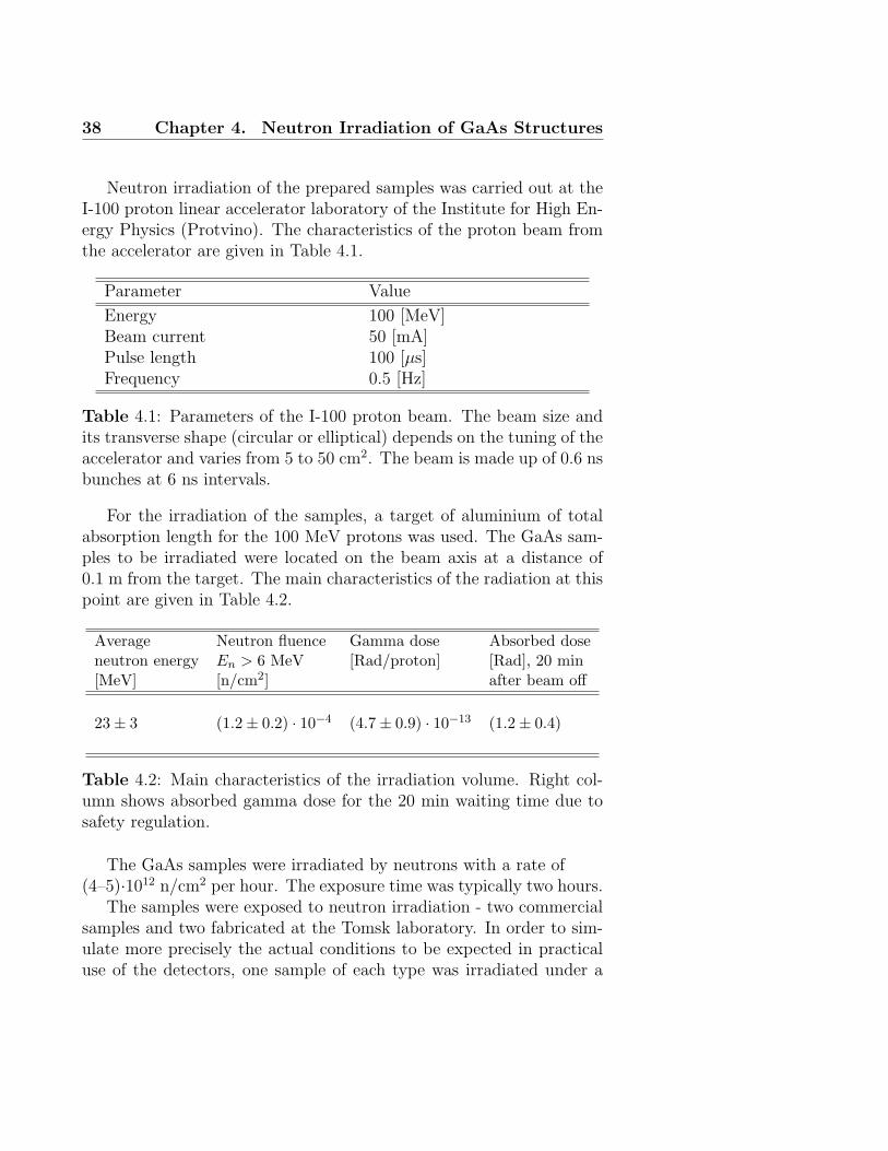
Figure 4.1: Resistivity of GaAs material as a function of radiationflux by fast protons, neutrons and electrons. (no is an initial density ofelectrons in GaAs.) Open symbols are earlier measurements by Tomskgroup. Solid circles are results from one of the neutron irradiated sam-ples. The lines are drawn to guide the eye.
When the low resistance GaAs material are exposed to high energyionizing radiation [41], compensation of the electrical conductivity hasbeen demonstrated. This compensation is found not to depend on
40 Chapter 4. Neutron Irradiation of GaAs Structures
either the type of initial conductivity or on single impurities, but doesdepend on the trapping of free charge carriers by radiation-induceddefects.
Figure 4.1 shows the change in resistivity of GaAs samples sub-jected to irradiation by fast protons, neutrons and electrons [45]. Theresistivity tends to a maximum value of 109 Ohm·cm independently ofthe type of irradiating particle. The increase in specific resistance isdue mainly to the reduction in the density of free charge carriers. Inour case, the initial compensation means that there is no further in-crease in specific resistance up to some limit of the neutron dose fromthe I-100 accelerator. For our samples of GaAs which have been com-pensated by iron, the typical resistance only begins to show an increasefor neutron fluences in excess of 1015 n/cm2 (Figure 4.1).
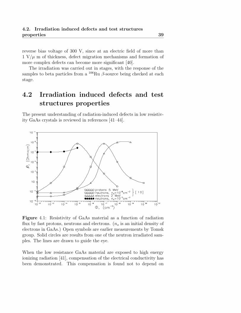
Figure 4.2: Forward I–V characteristic as a function of neutron irradi-ation. Regions I, II and III correspond to different current mechanisms.
The I-V characteristic variation with neutron irradiation was stud-ied using π-ν-n structures. The forward I-V characteristic is illustratedin Figure 4.2. The ohmic region of the characteristic (I) can be ob-served for both forward and reverse bias voltages of less than 0.1 V.The minority carrier lifetime, τ0, in the space charge region has beenmeasured from the slope of this part of the I-V curve and found to
4.2. Irradiation induced defects and test structuresproperties 41
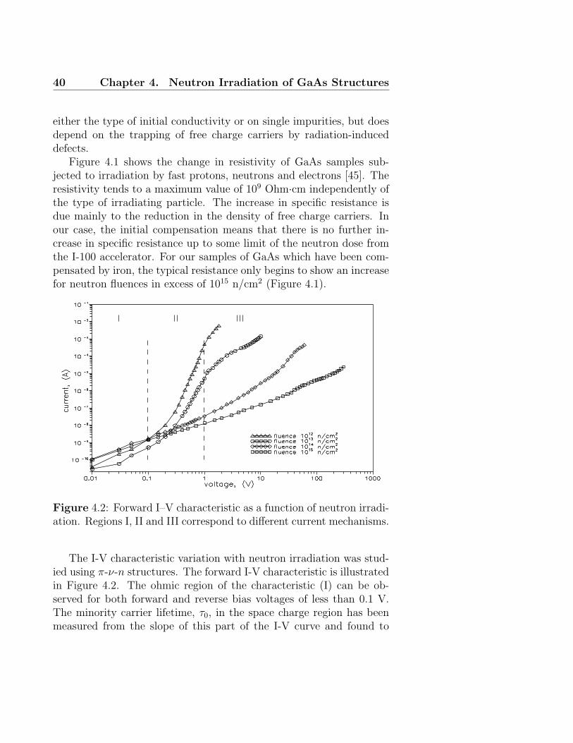
Figure 4.3: Reverse I–V characteristic as a function of neutron irradi-ation. Regions I, II and III correspond to different current mechanisms.
be independent of the irradiation and lies in the range 0.5 − 1 ns. Inthe recombination region (II) the forward characteristic changes signif-icantly. When the dose increases, it is observed that this part tendsto disappear, i.e. recombination in the space-charge region becomesnegligible in spite of the widening of this area of the volume charge.The third region (III), connected with the double injection of currentin the π–layer, has also changed: with increased dose this part of thecurrent becomes smaller and, ultimately, we see the transformation toan ohmic state. Estimation shows that when the dose increases, thespecific resistance of the thin π–layer also grows in proportion up to108 Ohm·cm (Figure 4.4). Regions II and III of the reverse bias branchalso become deformed (Figure 4.3).
Let us analyze the processes in the π–layer. There is a large increasein the resistance of the π–layer, as shown in Figure 4.4. A classicalconductivity modulation method was used to establish the lifetime ofthe minority carriers (electrons) in the π–layer. A fixed-length forwardbias rectangular pulse was applied to the structure, resulting in theinjection of electrons into the π–region from the displaced π-ν junction.In a fixed time interval the rectangular test pulse was applied to the
42 Chapter 4. Neutron Irradiation of GaAs Structures
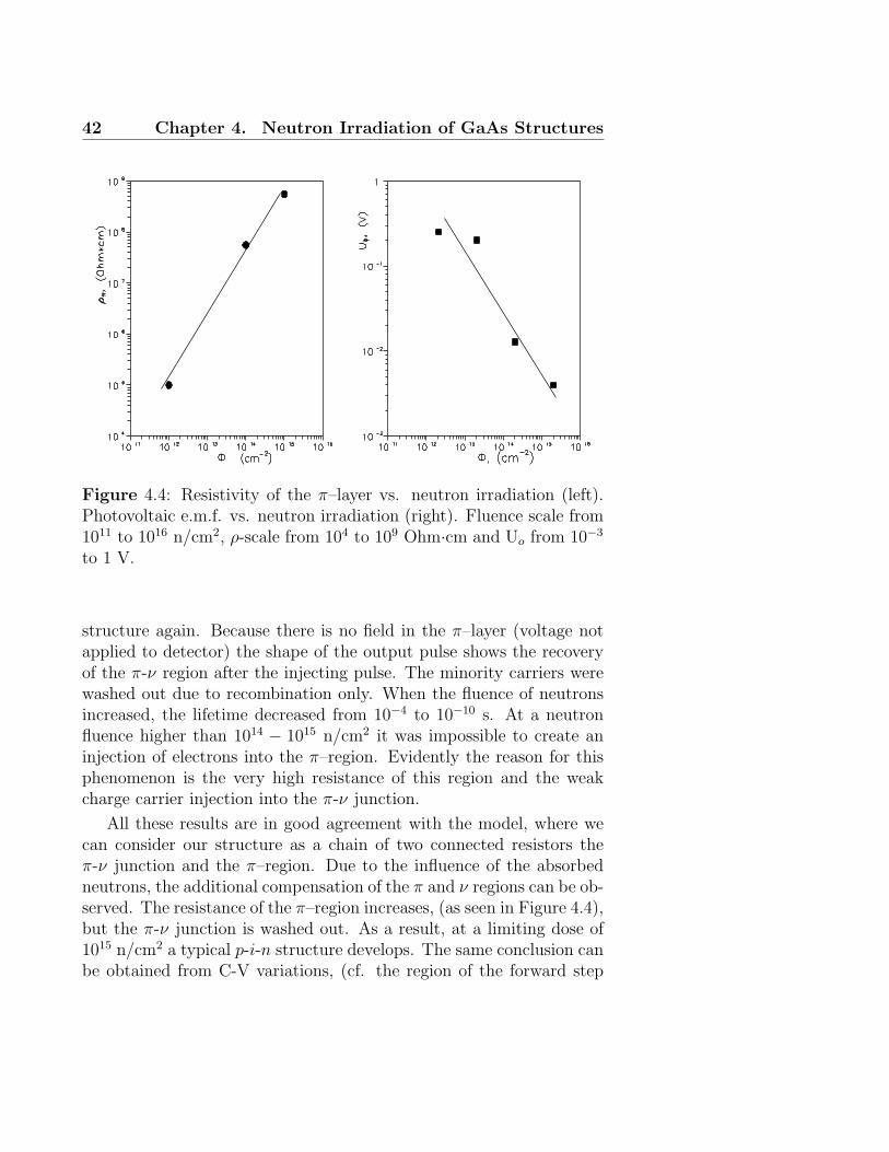
Figure 4.4: Resistivity of the π–layer vs. neutron irradiation (left).Photovoltaic e.m.f. vs. neutron irradiation (right). Fluence scale from1011 to 1016 n/cm2, ρ-scale from 104 to 109 Ohm·cm and Uo from 10−3
to 1 V.
structure again. Because there is no field in the π–layer (voltage notapplied to detector) the shape of the output pulse shows the recoveryof the π-ν region after the injecting pulse. The minority carriers werewashed out due to recombination only. When the fluence of neutronsincreased, the lifetime decreased from 10−4 to 10−10 s. At a neutronfluence higher than 1014 − 1015 n/cm2 it was impossible to create aninjection of electrons into the π–region. Evidently the reason for thisphenomenon is the very high resistance of this region and the weakcharge carrier injection into the π-ν junction.
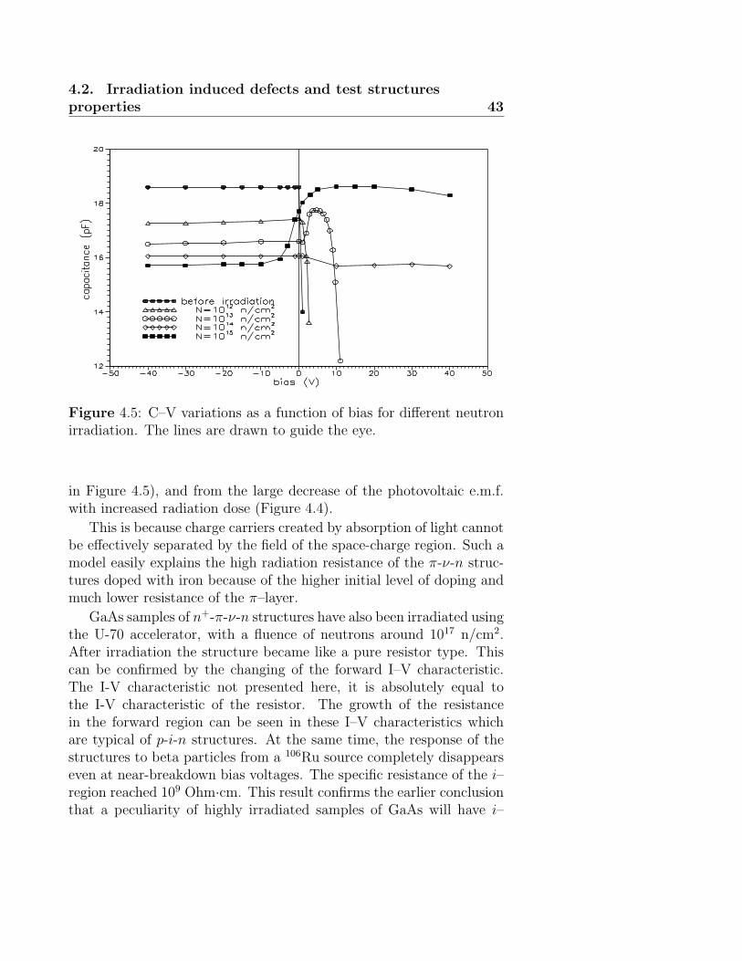
All these results are in good agreement with the model, where wecan consider our structure as a chain of two connected resistors theπ-ν junction and the π–region. Due to the influence of the absorbedneutrons, the additional compensation of the π and ν regions can be ob-served. The resistance of the π–region increases, (as seen in Figure 4.4),but the π-ν junction is washed out. As a result, at a limiting dose of1015 n/cm2 a typical p-i-n structure develops. The same conclusion canbe obtained from C-V variations, (cf. the region of the forward step
4.2. Irradiation induced defects and test structuresproperties 43
Figure 4.5: C–V variations as a function of bias for different neutronirradiation. The lines are drawn to guide the eye.
in Figure 4.5), and from the large decrease of the photovoltaic e.m.f.with increased radiation dose (Figure 4.4).
This is because charge carriers created by absorption of light cannotbe effectively separated by the field of the space-charge region. Such amodel easily explains the high radiation resistance of the π-ν-n struc-tures doped with iron because of the higher initial level of doping andmuch lower resistance of the π–layer.
GaAs samples of n+-π-ν-n structures have also been irradiated usingthe U-70 accelerator, with a fluence of neutrons around 1017 n/cm2.After irradiation the structure became like a pure resistor type. Thiscan be confirmed by the changing of the forward I–V characteristic.The I-V characteristic not presented here, it is absolutely equal tothe I-V characteristic of the resistor. The growth of the resistancein the forward region can be seen in these I–V characteristics whichare typical of p-i-n structures. At the same time, the response of thestructures to beta particles from a 106Ru source completely disappearseven at near-breakdown bias voltages. The specific resistance of the i–region reached 109 Ohm·cm. This result confirms the earlier conclusionthat a peculiarity of highly irradiated samples of GaAs will have i–
44 Chapter 4. Neutron Irradiation of GaAs Structures
Figure 4.6: Noise (RMS) vs. neutron irradiation. The lines are drawnto guide the eye.
type conductivity independently of the initial material’s conductivitytype [40]. This behavior is in agreement with the change of detectorcapacitance due to the creation of compensation impurities (centers)during irradiation (Figure 4.5).
4.3 Sensitivity of GaAs structures to min-
imum ionizing beta particles
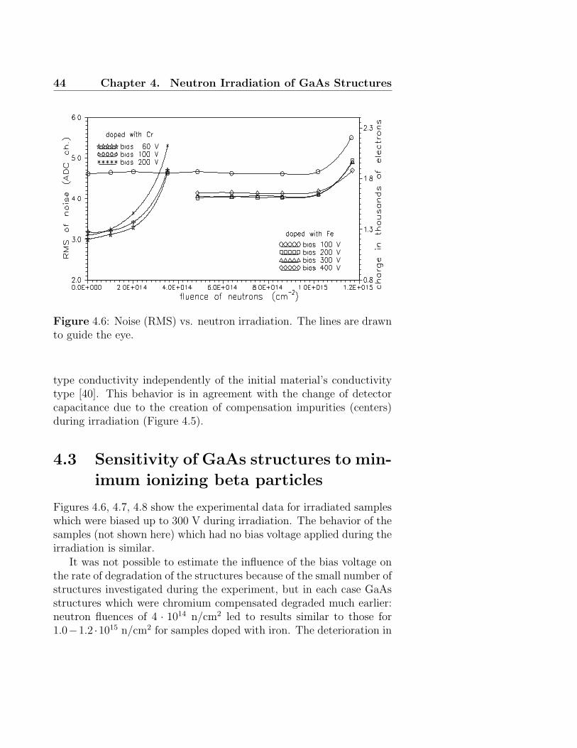
Figures 4.6, 4.7, 4.8 show the experimental data for irradiated sampleswhich were biased up to 300 V during irradiation. The behavior of thesamples (not shown here) which had no bias voltage applied during theirradiation is similar.
It was not possible to estimate the influence of the bias voltage onthe rate of degradation of the structures because of the small number ofstructures investigated during the experiment, but in each case GaAsstructures which were chromium compensated degraded much earlier:neutron fluences of 4 · 1014 n/cm2 led to results similar to those for1.0−1.2 ·1015 n/cm2 for samples doped with iron. The deterioration in
4.3. Sensitivity of GaAs structures to minimum ionizingbeta particles 45
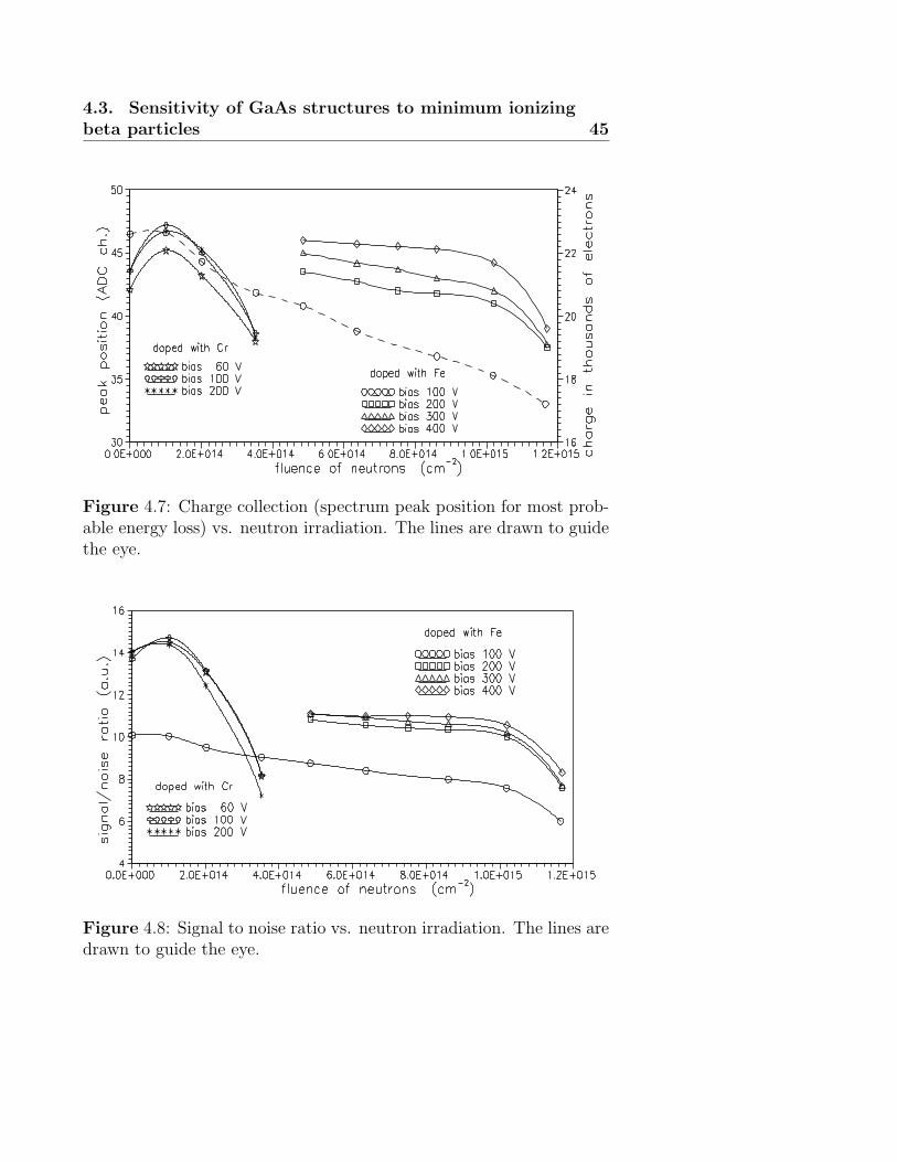
Figure 4.7: Charge collection (spectrum peak position for most prob-able energy loss) vs. neutron irradiation. The lines are drawn to guidethe eye.
Figure 4.8: Signal to noise ratio vs. neutron irradiation. The lines aredrawn to guide the eye.
46 Chapter 4. Neutron Irradiation of GaAs Structures
S/N ratio due to the irradiation was not more than 20% for the latter.
The much lower radiation resistance of chromium doped samplescan be explained by the following. To decrease the specific capacity ofthese structures (which leads to an increase in the S/N ratio for samplesbefore irradiation (Figure 4.8)), the sample processing used a chromiumconcentration which was ten times less than that of the iron in the caseof doping by the latter. It is well known that radiation-induced defectsin GaAs give deep trapping centers which have compensating propertieslike iron and chromium [46]. Consequently at a higher concentrationof the chromium or iron dopants the relative influence of created trapsat higher neutron fluence is smaller. One of the properties of GaAsafter irradiation is the decrease in the intensity of radiative recom-bination, Refs. [40–44], pointing to the predominant creation of non-radiative recombination centers. Significant distortion of the latticenear the radiation-induced defects leads to an increase of the probabil-ity of multi-phonon non-radiative recombination of charge carriers anddistortion of the lattice also accounts for the recombination-stimulatedmigration of defects [45].
All of this leads to a decrease of the lifetime of a non-equilibriumcharge carriers concentration in π– and ν–layers caused by ionizationby beta particles. For neutron fluences > 1015 n/cm2 full charge collec-tion requires an increase of the electric field in the structure so that thecharge collection time is not longer than the lifetime of non-equilibriumcharge carriers (Figure 4.7). As discussed in Section 4.2, during theneutron beam irradiation of GaAs, additional compensation of thesemiconductor takes place, leading to an increase in the specific re-sistance of the π– and ν–layers of the structure. The specific resistanceof the π–region can be approximately ten times that of other layers.It is supposed that the extension of the space-charge region with in-creasing reverse bias voltage will take place mainly in the ν–region butwith the increase of the specific resistance of the π–region, the volt-age decrease does not occur over the whole sensitive thickness of thesample. To create the required electric field inside the whole sensitiveregion of the sample, it is necessary to raise the bias voltage [19]. Thischange of the voltage distribution between π– and ν–layers togetherwith the decreased lifetime of non-equilibrium charge carriers leads tothe observed degradation of the sample response to beta particles.
4.4. Conclusion 47
4.4 Conclusion
Fe doped detectors based on laboratory grown material (Bridgeman)shows better radiation resistance compared to GaAs detectors basedon commercial (Czochralski) low resistivity Cr doped materials. Themain reason is assumed due to to the lower dopant concentration. GaAsstructures based on Czochralski low resistivity materials with increasedchromium doping concentration can be in principle created. It can beexpected that the radiation resistance of such structures will be similarto that of similar structures compensated by iron. The present resultsconfirm the possibility of the use of such structures as a basis for thefabrication of radiation-resistant coordinate detectors.
The diffusion technology for the formation of compensated high-resistivity GaAs layers on industrial substrates is now better under-stood. This ensures the reproducibility of the electrophysical charac-teristics of the devices and furthermore provides the necessary surfaceareas to permit the application of planar technology in the industrialfabrication of strip detectors.
Chapter 5
Irradiation in Mixed Beamat CERN
In this chapter results from irradiation of GaAs detectors at intenseparticles beam are presented. The irradiation was made just afterthe beryllium target in the special beam-line for the neutrino experi-ments. The target was bombarded with proton beams at 540 GeV atCERN. The study of the radiation resistance of the GaAs samples hasshown that their main characteristics (charge collection efficiency, sig-nal/noise ratio) degrade less than factor of two at the integral fluenceof 2·1014 particles·cm−2.
5.1 Introduction
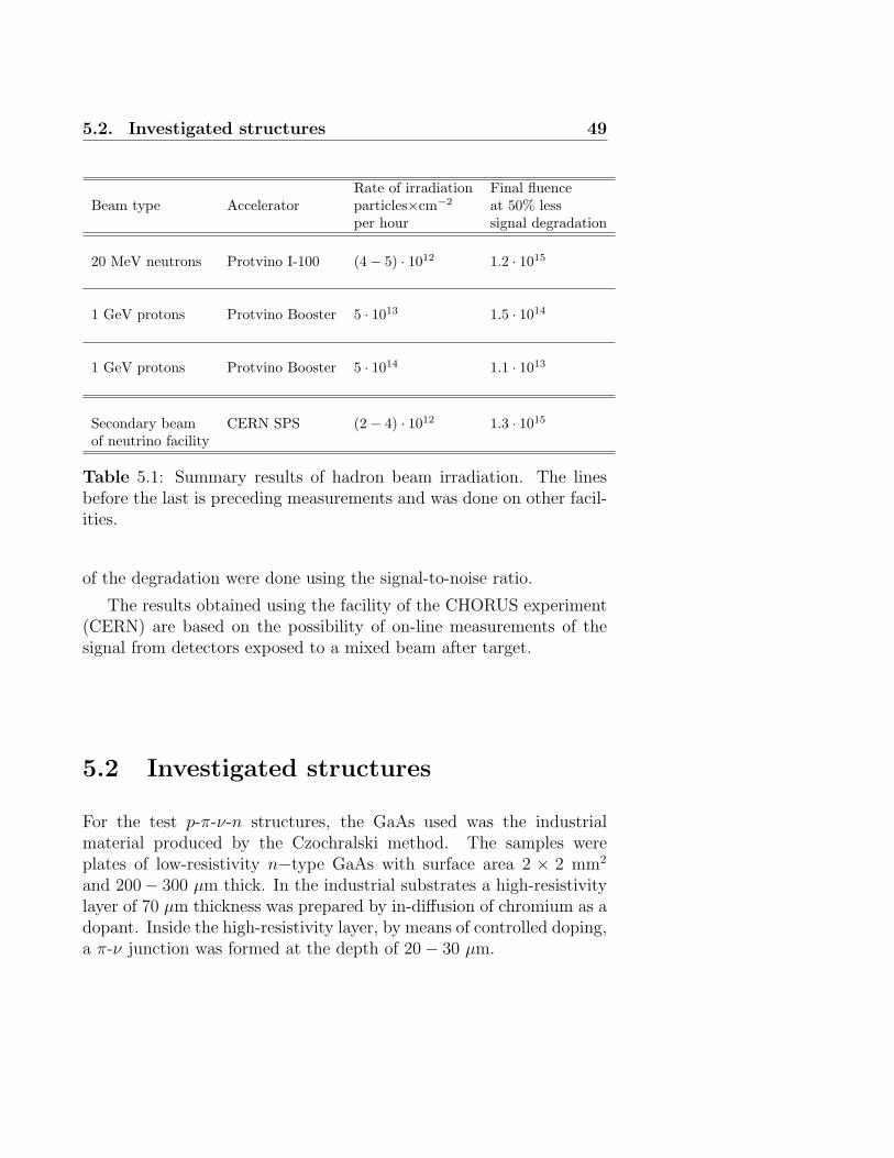
Proceeding from the data on GaAs detectors irradiation by varioustypes of particles, a hypothesis about the correlation between degra-dation of the properties of the detectors and the rate of irradiation isset forth. The results of the preceding investigations are summarizedin Table 5.1. Therefore a test was made in an environment with adifferent irradiation rate at CERN.
The 540 GeV proton beam from CERN SPS accelerator was sent tothe target with the following time structure: ten repeated cycles of twoextractions, 1.5 · 1015 protons each, separated by 2.76 s. Clearly, thedegradation of detectors is in proportion to the rate of irradiation inthe range (1.5–3)·1012 — 5 · 1014 part.×cm−2 per hour. The estimates
48
5.2. Investigated structures 49
Rate of irradiation Final fluenceBeam type Accelerator particles×cm−2 at 50% less
per hour signal degradation
20 MeV neutrons Protvino I-100 (4− 5) · 1012 1.2 · 1015
1 GeV protons Protvino Booster 5 · 1013 1.5 · 1014
1 GeV protons Protvino Booster 5 · 1014 1.1 · 1013
Secondary beam CERN SPS (2− 4) · 1012 1.3 · 1015
of neutrino facility
Table 5.1: Summary results of hadron beam irradiation. The linesbefore the last is preceding measurements and was done on other facil-ities.
of the degradation were done using the signal-to-noise ratio.
The results obtained using the facility of the CHORUS experiment(CERN) are based on the possibility of on-line measurements of thesignal from detectors exposed to a mixed beam after target.
5.2 Investigated structures
For the test p-π-ν-n structures, the GaAs used was the industrialmaterial produced by the Czochralski method. The samples wereplates of low-resistivity n−type GaAs with surface area 2 × 2 mm2
and 200− 300 µm thick. In the industrial substrates a high-resistivitylayer of 70 µm thickness was prepared by in-diffusion of chromium as adopant. Inside the high-resistivity layer, by means of controlled doping,a π-ν junction was formed at the depth of 20− 30 µm.
50 Chapter 5. Irradiation in Mixed Beam at CERN
5.3 Experimental details
The 4-channel data acquisition system was developed and manufac-tured in NIM standard to fit the special experimental area, which wasa remote pit. Using this system, the following measurements were done:
1. Identify of the beam spill number dumped from SPS onto target.This was required since the two spills per cycle differ.
2. Read-out the BCT (Beam-Current Transformer) counter datathat is proportional to the number of protons hitting the target.
3. Measure the signal response to the secondary particle beam.
The module control and data acquisition was made using a PC that wasconnected to the module through a serial port. The duration of a singlemeasurement cycle, with the bias voltage polarity fixed, was around 2.5hours. First, before placing the detectors along the secondary beam in
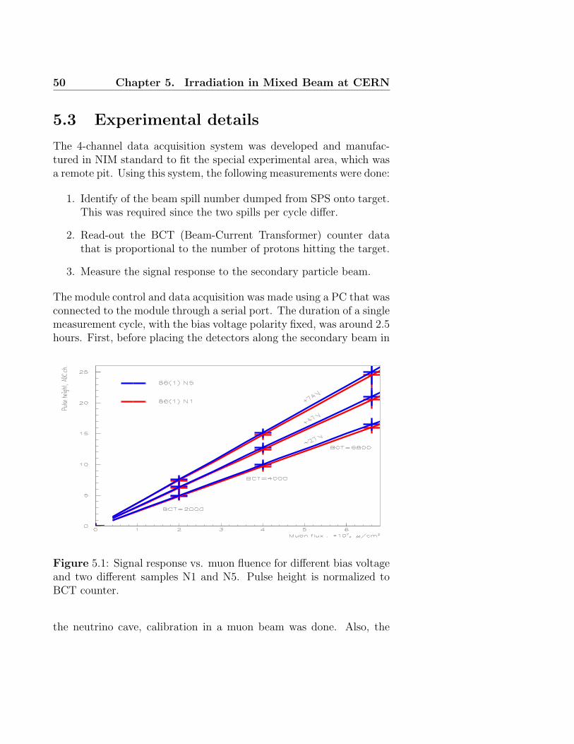
Figure 5.1: Signal response vs. muon fluence for different bias voltageand two different samples N1 and N5. Pulse height is normalized toBCT counter.
the neutrino cave, calibration in a muon beam was done. Also, the
5.4. Exposure in mixed beam, basic results 51
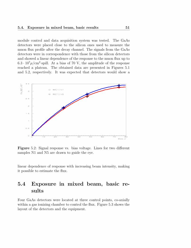
module control and data acquisition system was tested. The GaAsdetectors were placed close to the silicon ones used to measure themuon flux profile after the decay channel. The signals from the GaAsdetectors were in correspondence with those from the silicon detectorsand showed a linear dependence of the response to the muon flux up to6.3 · 107µ/cm2·spill. At a bias of 70 V, the amplitude of the responsereached a plateau. The obtained data are presented in Figures 5.1and 5.2, respectively. It was expected that detectors would show a
Figure 5.2: Signal response vs. bias voltage. Lines for two differentsamples N1 and N5 are drawn to guide the eye.
linear dependence of response with increasing beam intensity, makingit possible to estimate the flux.
5.4 Exposure in mixed beam, basic re-
sults
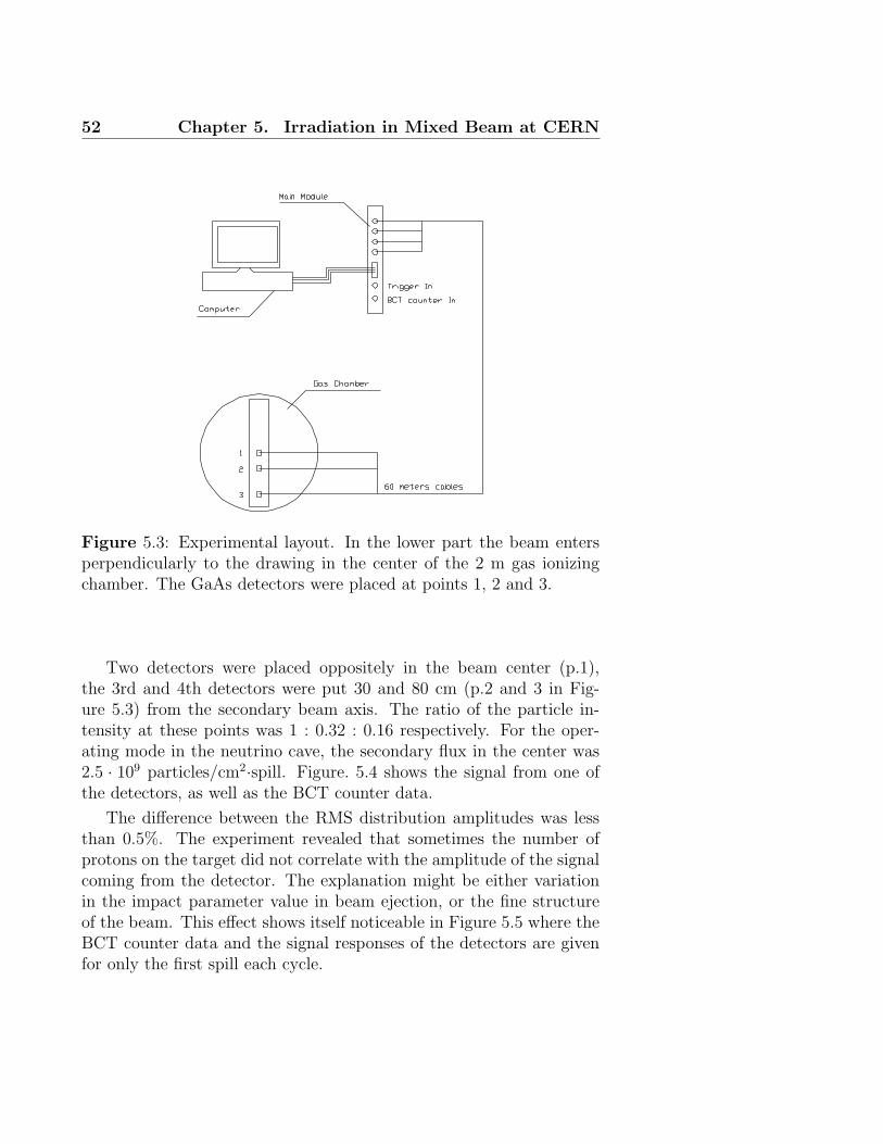
Four GaAs detectors were located at three control points, co-axiallywithin a gas ionizing chamber to control the flux. Figure 5.3 shows thelayout of the detectors and the equipment.
52 Chapter 5. Irradiation in Mixed Beam at CERN
Figure 5.3: Experimental layout. In the lower part the beam entersperpendicularly to the drawing in the center of the 2 m gas ionizingchamber. The GaAs detectors were placed at points 1, 2 and 3.
Two detectors were placed oppositely in the beam center (p.1),the 3rd and 4th detectors were put 30 and 80 cm (p.2 and 3 in Fig-ure 5.3) from the secondary beam axis. The ratio of the particle in-tensity at these points was 1 : 0.32 : 0.16 respectively. For the oper-ating mode in the neutrino cave, the secondary flux in the center was2.5 · 109 particles/cm2·spill. Figure. 5.4 shows the signal from one ofthe detectors, as well as the BCT counter data.
The difference between the RMS distribution amplitudes was lessthan 0.5%. The experiment revealed that sometimes the number ofprotons on the target did not correlate with the amplitude of the signalcoming from the detector. The explanation might be either variationin the impact parameter value in beam ejection, or the fine structureof the beam. This effect shows itself noticeable in Figure 5.5 where theBCT counter data and the signal responses of the detectors are givenfor only the first spill each cycle.
5.4. Exposure in mixed beam, basic results 53
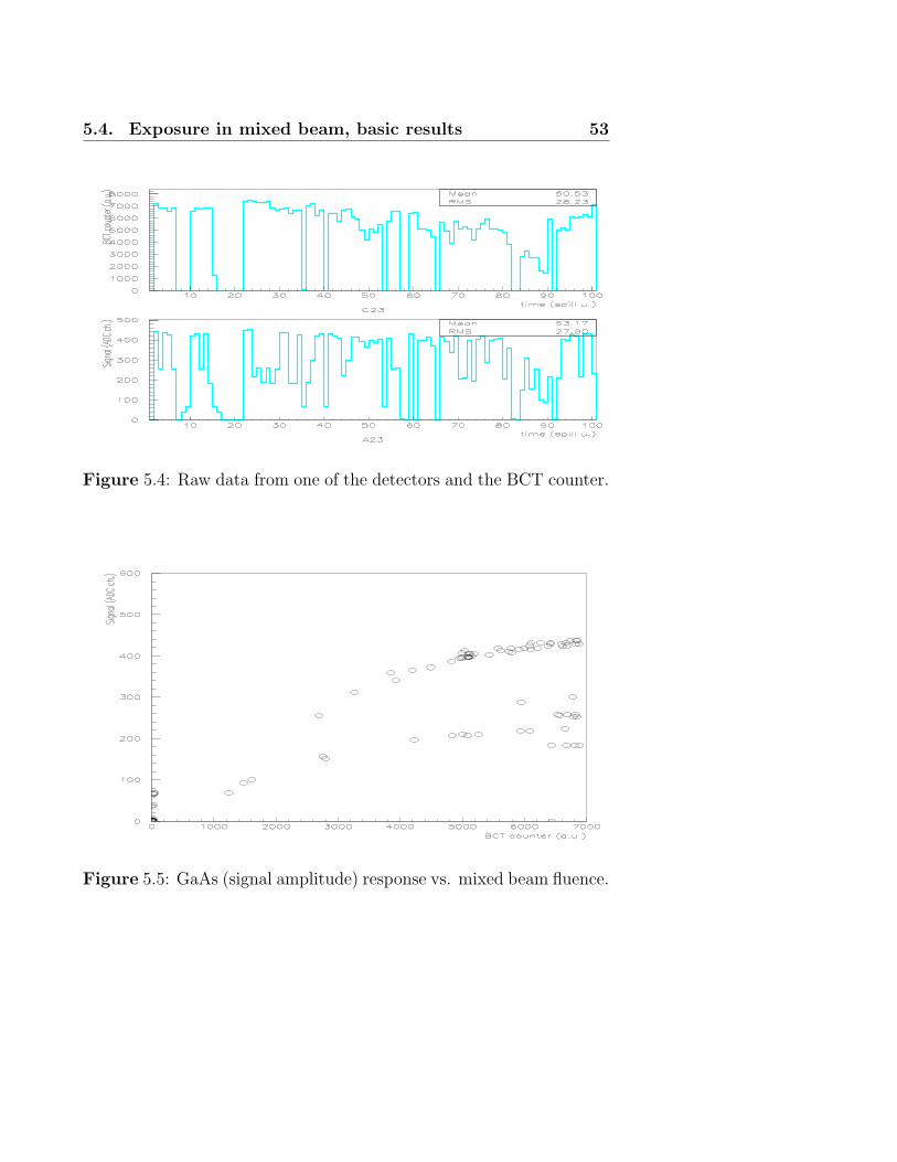
Figure 5.4: Raw data from one of the detectors and the BCT counter.
Figure 5.5: GaAs (signal amplitude) response vs. mixed beam fluence.
54 Chapter 5. Irradiation in Mixed Beam at CERN
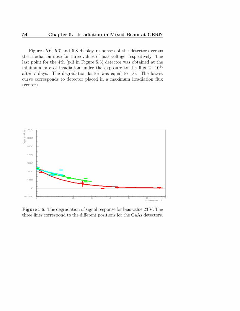
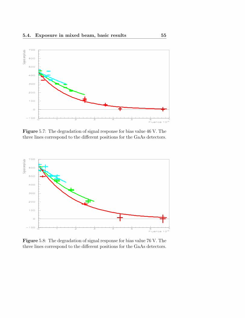
Figures 5.6, 5.7 and 5.8 display responses of the detectors versusthe irradiation dose for three values of bias voltage, respectively. Thelast point for the 4th (p.3 in Figure 5.3) detector was obtained at theminimum rate of irradiation under the exposure to the flux 2 · 1014
after 7 days. The degradation factor was equal to 1.6. The lowestcurve corresponds to detector placed in a maximum irradiation flux(center).
Figure 5.6: The degradation of signal response for bias value 23 V. Thethree lines correspond to the different positions for the GaAs detectors.
5.4. Exposure in mixed beam, basic results 55
Figure 5.7: The degradation of signal response for bias value 46 V. Thethree lines correspond to the different positions for the GaAs detectors.
Figure 5.8: The degradation of signal response for bias value 76 V. Thethree lines correspond to the different positions for the GaAs detectors.
56 Chapter 5. Irradiation in Mixed Beam at CERN
5.5 Signal estimation
To measure the flux, only the data of the gas ionizing chambers wasused because of the nonlinear response of the GaAs detectors to ion-ization. The signal amplitude of the detector can be written as:
U =[( dE
dxΦ
∆Ecr
· qe
)/ts
]Rin (5.1)
where,
dEdx
– ionizing energy loss;
Φ – flux;
∆Ecr – electron-hole pair creation energy;
qe – charge of electron;
Rin – input impedance of amplifier;
ts – spill time.
A simple calculation using(5.1) reveals that at full charge collection,the signal amplitude would be around 100 V with Rin = 1 MOhm. Thesignals ∼ 20 V that are observed at the bias voltage 70 V testify tothe fact that the basic signal production mechanism is of drift nature.The value of the signal relaxation time after spill transition, providedone takes into account that the cable length is 60 m and the totalcapacitance of the detector plus cable is 2500 pF, also speaks in favor ofthe absence of either breakdown, or current avalanche in the detectors.
The data shows that the degradation of the detectors, as expected,is a function of the irradiation rate.

Chapter 6
Microstrip Detectors Test
In this chapter the results of the first steps of studying pioneering GaAsprototypes of radiation resistant coordinate detectors using charge par-ticle beams are presented. The structure design of two detector pro-totypes with 150 µm and 50 µm pitch and their main characteristicsare described. The results of radiation tests show good operating con-ditions for protons and neutrons with fluxes up to 2 · 1014 p/cm2, 1 ·1015 n/cm2 and γ-rays absorbed dose up to 110 kGy in CH(polyethylene)-equivalent. The response of the detectors to the charge particles andthe detection efficiency have been measured.
57
58 Chapter 6. Microstrip Detectors Test
6.1 Main parameters of the microstrip de-
tectors
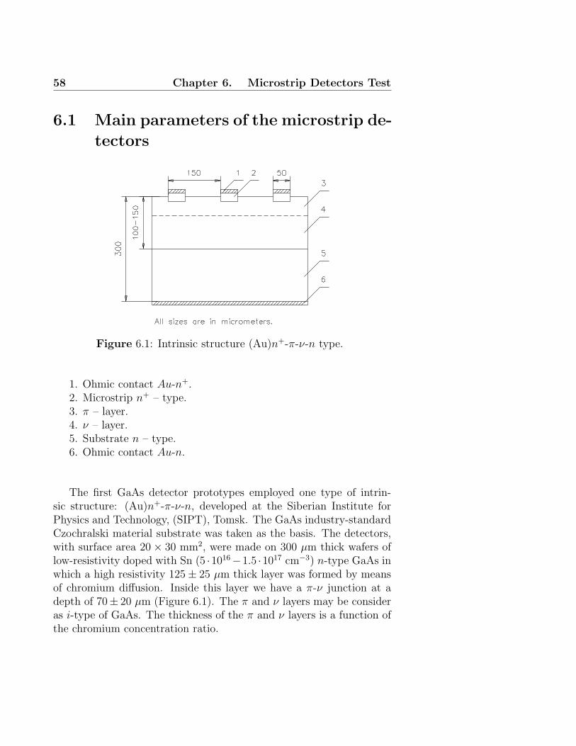
Figure 6.1: Intrinsic structure (Au)n+-π-ν-n type.
1. Ohmic contact Au-n+.2. Microstrip n+ – type.3. π – layer.4. ν – layer.5. Substrate n – type.6. Ohmic contact Au-n.
The first GaAs detector prototypes employed one type of intrin-sic structure: (Au)n+-π-ν-n, developed at the Siberian Institute forPhysics and Technology, (SIPT), Tomsk. The GaAs industry-standardCzochralski material substrate was taken as the basis. The detectors,with surface area 20 × 30 mm2, were made on 300 µm thick wafers oflow-resistivity doped with Sn (5 ·1016−1.5 ·1017 cm−3) n-type GaAs inwhich a high resistivity 125± 25 µm thick layer was formed by meansof chromium diffusion. Inside this layer we have a π-ν junction at adepth of 70± 20 µm (Figure 6.1). The π and ν layers may be consideras i-type of GaAs. The thickness of the π and ν layers is a function ofthe chromium concentration ratio.
6.1. Main parameters of the microstrip detectors 59
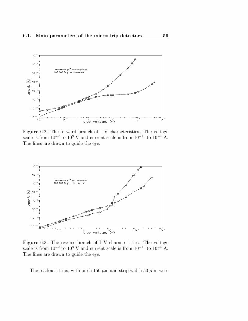
Figure 6.2: The forward branch of I–V characteristics. The voltagescale is from 10−2 to 103 V and current scale is from 10−11 to 10−4 A.The lines are drawn to guide the eye.
Figure 6.3: The reverse branch of I–V characteristics. The voltagescale is from 10−2 to 103 V and current scale is from 10−11 to 10−4 A.The lines are drawn to guide the eye.
The readout strips, with pitch 150 µm and strip width 50 µm, were
60 Chapter 6. Microstrip Detectors Test
formed from n+-type GaAs with Au on top. The I–V characteristics forthe (Au)n+-π-ν-n detector, measured for a single strip, are presentedin Figure 6.2 and Figure 6.3. The (Au)n+-π-ν-n detector have twoback-to-back junctions: n+-π and π-ν. Here ”forward” and ”reverse”bias voltages refer to the π-ν junction.
6.2 Experimental set-up
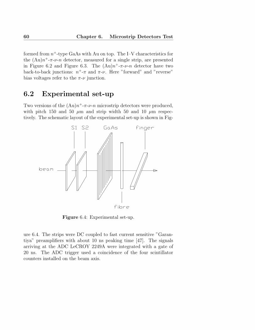
Two versions of the (Au)n+-π-ν-n microstrip detectors were produced,with pitch 150 and 50 µm and strip width 50 and 10 µm respec-tively. The schematic layout of the experimental set-up is shown in Fig-
Figure 6.4: Experimental set-up.
ure 6.4. The strips were DC coupled to fast current sensitive ”Garan-tiya” preamplifiers with about 10 ns peaking time [47]. The signalsarriving at the ADC LeCROY 2249A were integrated with a gate of20 ns. The ADC trigger used a coincidence of the four scintillatorcounters installed on the beam axis.
6.3. The beam test results 61
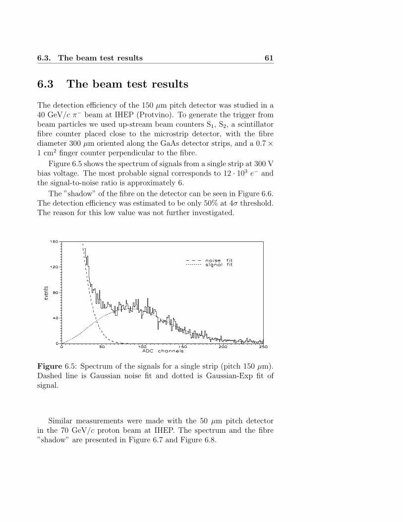
6.3 The beam test results
The detection efficiency of the 150 µm pitch detector was studied in a40 GeV/c π− beam at IHEP (Protvino). To generate the trigger frombeam particles we used up-stream beam counters S1, S2, a scintillatorfibre counter placed close to the microstrip detector, with the fibrediameter 300 µm oriented along the GaAs detector strips, and a 0.7×1 cm2 finger counter perpendicular to the fibre.
Figure 6.5 shows the spectrum of signals from a single strip at 300 Vbias voltage. The most probable signal corresponds to 12 · 103 e− andthe signal-to-noise ratio is approximately 6.
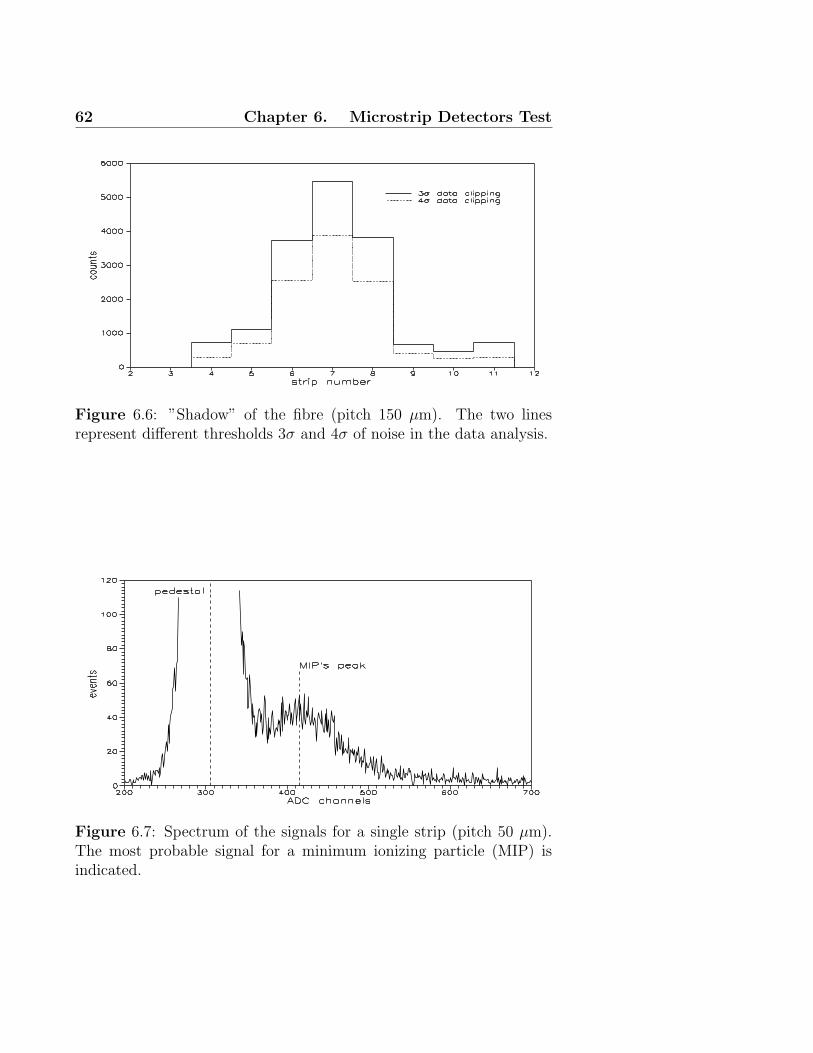
The ”shadow” of the fibre on the detector can be seen in Figure 6.6.The detection efficiency was estimated to be only 50% at 4σ threshold.The reason for this low value was not further investigated.
Figure 6.5: Spectrum of the signals for a single strip (pitch 150 µm).Dashed line is Gaussian noise fit and dotted is Gaussian-Exp fit ofsignal.
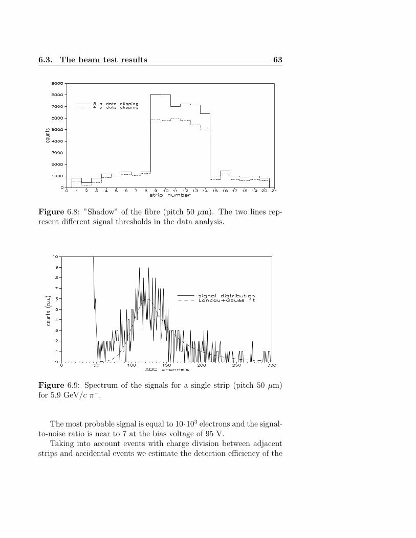
Similar measurements were made with the 50 µm pitch detectorin the 70 GeV/c proton beam at IHEP. The spectrum and the fibre”shadow” are presented in Figure 6.7 and Figure 6.8.
62 Chapter 6. Microstrip Detectors Test
Figure 6.6: ”Shadow” of the fibre (pitch 150 µm). The two linesrepresent different thresholds 3σ and 4σ of noise in the data analysis.
Figure 6.7: Spectrum of the signals for a single strip (pitch 50 µm).The most probable signal for a minimum ionizing particle (MIP) isindicated.
6.3. The beam test results 63
Figure 6.8: ”Shadow” of the fibre (pitch 50 µm). The two lines rep-resent different signal thresholds in the data analysis.
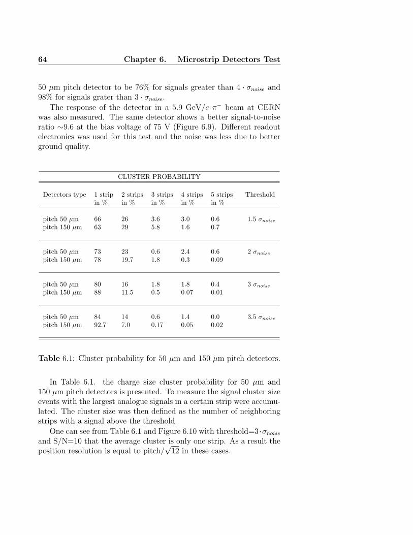
Figure 6.9: Spectrum of the signals for a single strip (pitch 50 µm)for 5.9 GeV/c π−.
The most probable signal is equal to 10·103 electrons and the signal-to-noise ratio is near to 7 at the bias voltage of 95 V.
Taking into account events with charge division between adjacentstrips and accidental events we estimate the detection efficiency of the
64 Chapter 6. Microstrip Detectors Test
50 µm pitch detector to be 76% for signals greater than 4 · σnoise and98% for signals grater than 3 · σnoise.
The response of the detector in a 5.9 GeV/c π− beam at CERNwas also measured. The same detector shows a better signal-to-noiseratio ∼9.6 at the bias voltage of 75 V (Figure 6.9). Different readoutelectronics was used for this test and the noise was less due to betterground quality.
CLUSTER PROBABILITY
Detectors type 1 strip 2 strips 3 strips 4 strips 5 strips Thresholdin % in % in % in % in %
pitch 50 µm 66 26 3.6 3.0 0.6 1.5 σnoise
pitch 150 µm 63 29 5.8 1.6 0.7
pitch 50 µm 73 23 0.6 2.4 0.6 2 σnoise
pitch 150 µm 78 19.7 1.8 0.3 0.09
pitch 50 µm 80 16 1.8 1.8 0.4 3 σnoise
pitch 150 µm 88 11.5 0.5 0.07 0.01
pitch 50 µm 84 14 0.6 1.4 0.0 3.5 σnoise
pitch 150 µm 92.7 7.0 0.17 0.05 0.02
Table 6.1: Cluster probability for 50 µm and 150 µm pitch detectors.
In Table 6.1. the charge size cluster probability for 50 µm and150 µm pitch detectors is presented. To measure the signal cluster sizeevents with the largest analogue signals in a certain strip were accumu-lated. The cluster size was then defined as the number of neighboringstrips with a signal above the threshold.
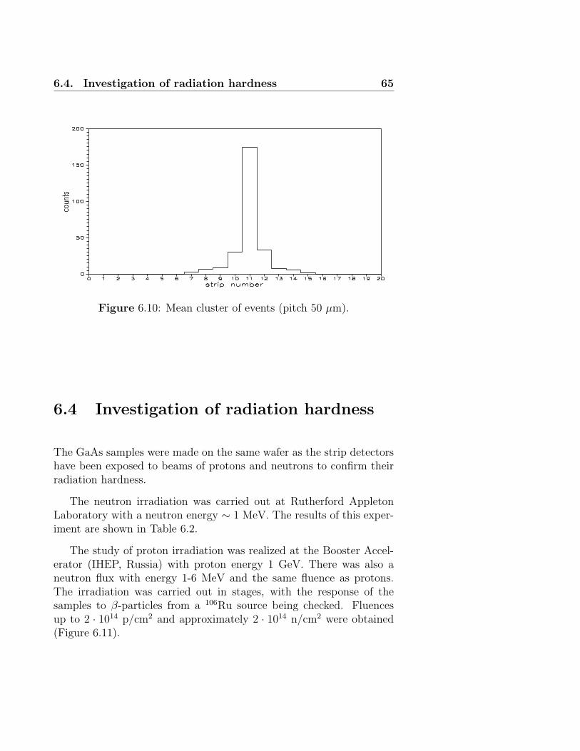
One can see from Table 6.1 and Figure 6.10 with threshold=3 ·σnoise
and S/N=10 that the average cluster is only one strip. As a result theposition resolution is equal to pitch/
√12 in these cases.
6.4. Investigation of radiation hardness 65
Figure 6.10: Mean cluster of events (pitch 50 µm).
6.4 Investigation of radiation hardness
The GaAs samples were made on the same wafer as the strip detectorshave been exposed to beams of protons and neutrons to confirm theirradiation hardness.
The neutron irradiation was carried out at Rutherford AppletonLaboratory with a neutron energy ∼ 1 MeV. The results of this exper-iment are shown in Table 6.2.
The study of proton irradiation was realized at the Booster Accel-erator (IHEP, Russia) with proton energy 1 GeV. There was also aneutron flux with energy 1-6 MeV and the same fluence as protons.The irradiation was carried out in stages, with the response of thesamples to β-particles from a 106Ru source being checked. Fluencesup to 2 · 1014 p/cm2 and approximately 2 · 1014 n/cm2 were obtained(Figure 6.11).
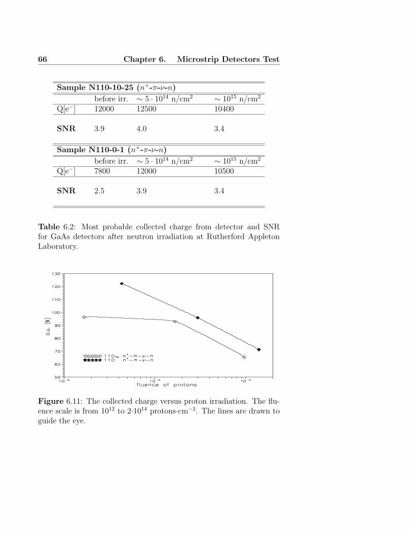
66 Chapter 6. Microstrip Detectors Test
Sample N110-10-25 (n+-π-ν-n)
before irr. ∼ 5 · 1014 n/cm2 ∼ 1015 n/cm2
Q[e−] 12000 12500 10400
SNR 3.9 4.0 3.4
Sample N110-0-1 (n+-π-ν-n)
before irr. ∼ 5 · 1014 n/cm2 ∼ 1015 n/cm2
Q[e−] 7800 12000 10500
SNR 2.5 3.9 3.4
Table 6.2: Most probable collected charge from detector and SNRfor GaAs detectors after neutron irradiation at Rutherford AppletonLaboratory.
Figure 6.11: The collected charge versus proton irradiation. The flu-ence scale is from 1012 to 2·1014 protons·cm−2. The lines are drawn toguide the eye.
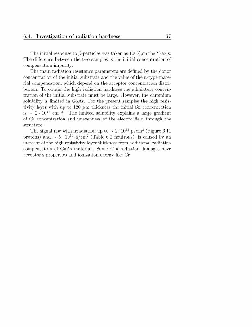
6.4. Investigation of radiation hardness 67
The initial response to β-particles was taken as 100%,on the Y-axis.The difference between the two samples is the initial concentration ofcompensation impurity.
The main radiation resistance parameters are defined by the donorconcentration of the initial substrate and the value of the n-type mate-rial compensation, which depend on the acceptor concentration distri-bution. To obtain the high radiation hardness the admixture concen-tration of the initial substrate must be large. However, the chromiumsolubility is limited in GaAs. For the present samples the high resis-tivity layer with up to 120 µm thickness the initial Sn concentrationis ∼ 2 · 1017 cm−3. The limited solubility explains a large gradientof Cr concentration and unevenness of the electric field through thestructure.
The signal rise with irradiation up to ∼ 2 · 1013 p/cm2 (Figure 6.11protons) and ∼ 5 · 1014 n/cm2 (Table 6.2 neutrons), is caused by anincrease of the high resistivity layer thickness from additional radiationcompensation of GaAs material. Some of a radiation damages haveacceptor’s properties and ionization energy like Cr.
Chapter 7
GaAs detectors forα-particles and heavy ionsspectrometry
7.1 Introduction
One main requirement for the fabrication of detectors for α-particlesand heavy ions spectrometry is the uniformity of the detector thicknessand its electrophysical characteristics. Only in this case will fluctua-tions of the particles energy losses be less or comparable to the statis-tical fluctuations of the created charge, which is formed by the particlein the detector structure. Detectors based on GaAs, due to its wideband gap (Eg=1.43 eV) and high electron mobility (µ=8600 cm2/Vs),offers the prospect of high speed particles detection and signal process-ing. The GaAs wafers are generally prepared by means of liquid-phaseepitaxy and the results of studies of such detectors can be found inreferences [48–53]. The aim of the present work is to study chargedparticle GaAs detectors fabricated by means of vapour-phase epitaxy(VPE) in Siberian Institute for Physics and Technology, Tomsk, Rus-sia.
68
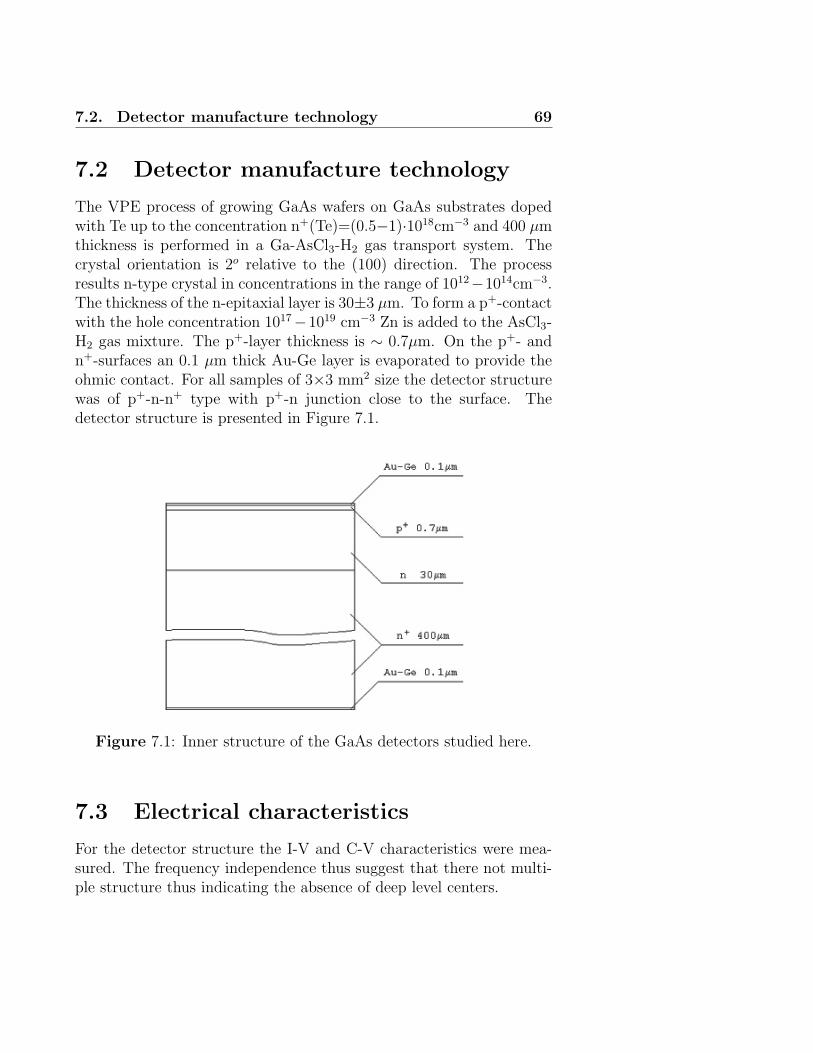
7.2. Detector manufacture technology 69
7.2 Detector manufacture technology
The VPE process of growing GaAs wafers on GaAs substrates dopedwith Te up to the concentration n+(Te)=(0.5−1)·1018cm−3 and 400 µmthickness is performed in a Ga-AsCl3-H2 gas transport system. Thecrystal orientation is 2o relative to the (100) direction. The processresults n-type crystal in concentrations in the range of 1012−1014cm−3.The thickness of the n-epitaxial layer is 30±3 µm. To form a p+-contactwith the hole concentration 1017−1019 cm−3 Zn is added to the AsCl3-H2 gas mixture. The p+-layer thickness is ∼ 0.7µm. On the p+- andn+-surfaces an 0.1 µm thick Au-Ge layer is evaporated to provide theohmic contact. For all samples of 3×3 mm2 size the detector structurewas of p+-n-n+ type with p+-n junction close to the surface. Thedetector structure is presented in Figure 7.1.
Figure 7.1: Inner structure of the GaAs detectors studied here.
7.3 Electrical characteristics
For the detector structure the I-V and C-V characteristics were mea-sured. The frequency independence thus suggest that there not multi-ple structure thus indicating the absence of deep level centers.
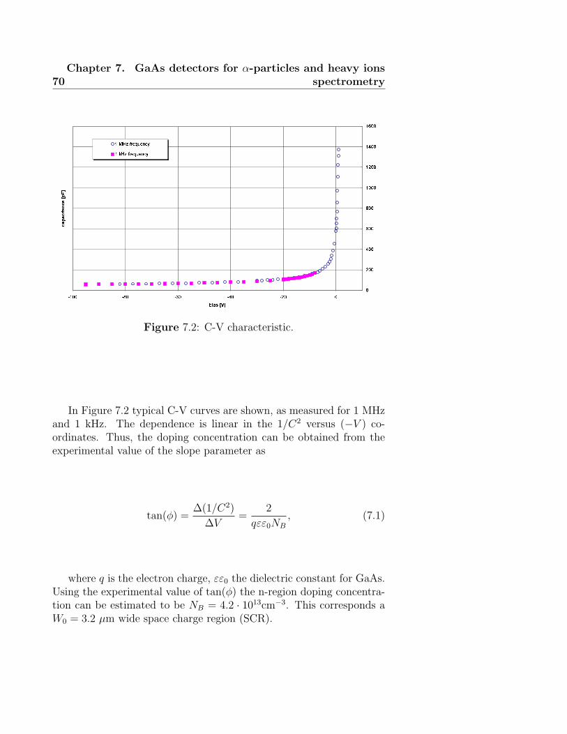
70Chapter 7. GaAs detectors for α-particles and heavy ions
spectrometry
�
���
���
���
���
����
����
����
����
���� ��� ��� ��� ��� �
�� ��
���������������
� ��� ������ !"
� #�� ������ !"
Figure 7.2: C-V characteristic.
In Figure 7.2 typical C-V curves are shown, as measured for 1 MHzand 1 kHz. The dependence is linear in the 1/C2 versus (−V ) co-ordinates. Thus, the doping concentration can be obtained from theexperimental value of the slope parameter as
tan(φ) =∆(1/C2)
∆V=
2
qεε0NB
, (7.1)
where q is the electron charge, εε0 the dielectric constant for GaAs.Using the experimental value of tan(φ) the n-region doping concentra-tion can be estimated to be NB = 4.2 · 1013cm−3. This corresponds aW0 = 3.2 µm wide space charge region (SCR).
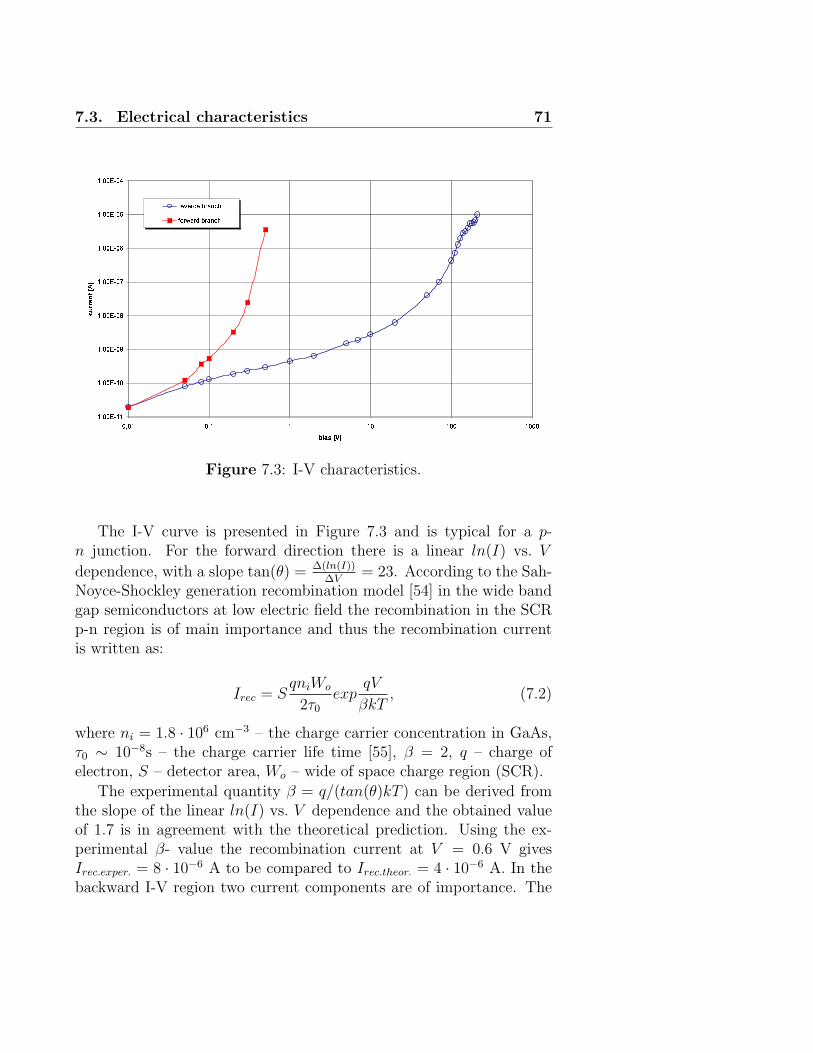
7.3. Electrical characteristics 71
��������
��������
��������
��������
��������
��������
�������
�������
���� ��� � �� ��� ������ � ���
����������
������� �� !�"#$�% �& �� !�"
Figure 7.3: I-V characteristics.
The I-V curve is presented in Figure 7.3 and is typical for a p-n junction. For the forward direction there is a linear ln(I) vs. V
dependence, with a slope tan(θ) = ∆(ln(I))∆V
= 23. According to the Sah-Noyce-Shockley generation recombination model [54] in the wide bandgap semiconductors at low electric field the recombination in the SCRp-n region is of main importance and thus the recombination currentis written as:
Irec = SqniWo
2τ0
expqV
βkT, (7.2)
where ni = 1.8 · 106 cm−3 – the charge carrier concentration in GaAs,τ0 ∼ 10−8s – the charge carrier life time [55], β = 2, q – charge ofelectron, S – detector area, Wo – wide of space charge region (SCR).
The experimental quantity β = q/(tan(θ)kT ) can be derived fromthe slope of the linear ln(I) vs. V dependence and the obtained valueof 1.7 is in agreement with the theoretical prediction. Using the ex-perimental β- value the recombination current at V = 0.6 V givesIrec.exper. = 8 · 10−6 A to be compared to Irec.theor. = 4 · 10−6 A. In thebackward I-V region two current components are of importance. The
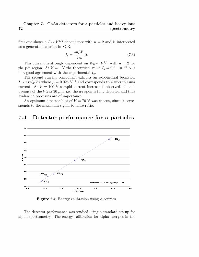
72Chapter 7. GaAs detectors for α-particles and heavy ions
spectrometry
first one shows a I ∼ V 1/n dependence with n = 2 and is interpretedas a generation current in SCR.
Ig =qniW0
2τ0
S. (7.3)
This current is strongly dependent on W0 ∼ V 1/n with n = 2 forthe p-n region. At V = 1 V the theoretical value Ig = 9.2 · 10−10 A isin a good agreement with the experimental Ig.
The second current component exhibits an exponential behavior,I ∼ exp(µV ) where µ = 0.025 V−1 and corresponds to a microplasmacurrent. At V = 100 V a rapid current increase is observed. This isbecause of the W0 ' 30 µm, i.e. the n-region is fully depleted and thusavalanche processes are of importance.
An optimum detector bias of V = 70 V was chosen, since it corre-sponds to the maximum signal to noise ratio.
7.4 Detector performance for α-particles
�������� � ���� ������ ������ � ������
���
���
���
���
���
���
���
���
���� ���� ���� ���� ���� ��� !����"#"$%& '(")*
+,-../01
2334
23567 23867
29:6;
2324
Figure 7.4: Energy calibration using α-sources.
The detector performance was studied using a standard set-up foralpha spectrometry. The energy calibration for alpha energies in the
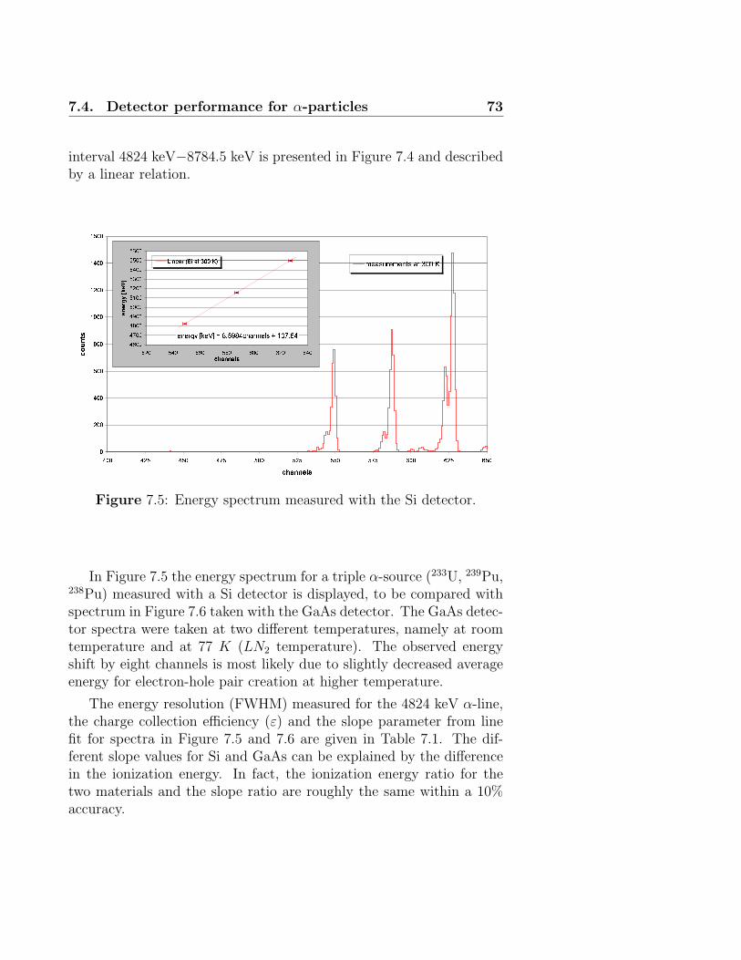
7.4. Detector performance for α-particles 73
interval 4824 keV−8784.5 keV is presented in Figure 7.4 and describedby a linear relation.
�
���
���
���
���
����
����
����
����
��� ��� ��� ��� ��� ��� ��� ��� ��� ��� ������� �
������
������������ �� ��� �
! "#$ %& '( ) *+,-*./01!! 23 4 567+,.89::8;::8<::8=::>:::>?::>@::>A::>8::>>::>9::
>@: >8: >9: ><: 9:: 9@: 98:BCDEEFGH
IJIKLMNOIPQ
RSTUVW XYS VZ [�� \]
Figure 7.5: Energy spectrum measured with the Si detector.
In Figure 7.5 the energy spectrum for a triple α-source (233U, 239Pu,238Pu) measured with a Si detector is displayed, to be compared withspectrum in Figure 7.6 taken with the GaAs detector. The GaAs detec-tor spectra were taken at two different temperatures, namely at roomtemperature and at 77 K (LN2 temperature). The observed energyshift by eight channels is most likely due to slightly decreased averageenergy for electron-hole pair creation at higher temperature.
The energy resolution (FWHM) measured for the 4824 keV α-line,the charge collection efficiency (ε) and the slope parameter from linefit for spectra in Figure 7.5 and 7.6 are given in Table 7.1. The dif-ferent slope values for Si and GaAs can be explained by the differencein the ionization energy. In fact, the ionization energy ratio for thetwo materials and the slope ratio are roughly the same within a 10%accuracy.
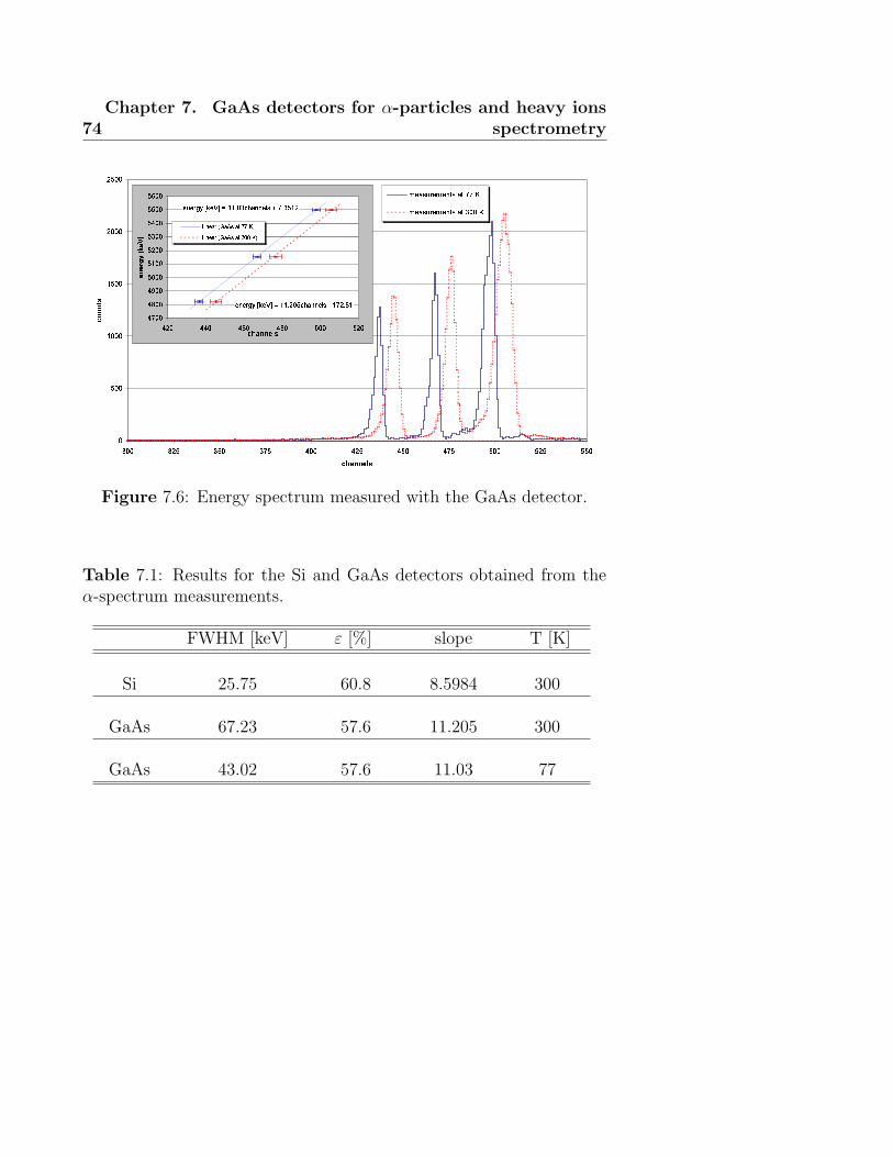
74Chapter 7. GaAs detectors for α-particles and heavy ions
spectrometry
�
���
����
����
����
����
��� ��� ��� ��� ��� ��� ��� ��� ��� ��� �������
������
������������ �� �� �
������������ �� ��� ����� ! "#�$% & ''()*+,-���./ 0 1(*2'3
���� ! "#�$% & ''(3)2+,-���./ 4 '13(5'61))67))68))2)))2'))23))2*))26))22))25))
63) 66) 65) 67) 2)) 23)����
9:9;<=>?9@A
BCDEFG HIFJK FL MM NOBCDEFG HIFJK FL PQQ NO
Figure 7.6: Energy spectrum measured with the GaAs detector.
Table 7.1: Results for the Si and GaAs detectors obtained from theα-spectrum measurements.
FWHM [keV] ε [%] slope T [K]
Si 25.75 60.8 8.5984 300
GaAs 67.23 57.6 11.205 300
GaAs 43.02 57.6 11.03 77
7.4. Detector performance for α-particles 75
Conclusion
The present studies of a GaAs detector based on an epitaxial materialshowed a linear signal response in a wide alpha energy range. Thegood results for the energy resolution and the charge collection effi-ciency indicates abilities for α- spectrometry applications. This maybe well valid even for heavy ion detection, which can be a subject forfurther studies. The Si detectors give us a better resolution, but themain advantage of GaAs detectors is the radiation hardness which isan important for heavy ion spectrometry. To obtain radiation hardnessfor ion spectrometry applications, investigations should be continuedwith compensated GaAs.
Chapter 8
X-ray Irradiation of SiliconDetectors
Introduction
Silicon detectors are used extensively in X-ray imaging, either as pri-mary detector for the X-rays or in combination with a scintillator asa detector for secondary light. Long term stability is usually desiredfor any application in medical imaging or non-destructive testing, andany radiation related measurable impact on the detector performancemust be low or corrected for. The radiation hardness thus plays animportant role for the choice of the detector material. Applicationsrange from detectors for portal imaging to detectors for computed to-mography (CT) and mammography. The impact of ionizing radiationon Silicon detectors has been described in the literature [56, 57], how-ever all studies have been performed at higher energies, e.g. using a60Co gamma-ray source or hadrons. The damage depends on the radi-ation energy. X-rays at high enough energy, 145-173 keV accordinglyto [58,59], create defects in the Silicon lattice at the Si/SiO2 interface.Data for these higher energies cannot be extrapolated to lower ener-gies, less than 50 keV in our case. Z. Marka et al. [60] have studiedthe long-term time dependence of the observed leakage current in sam-ples irradiated with low energy X-ray at 10 keV. They investigated thedamage enhanced electron transport across thin oxides in Si/SiO2.
The behavior of a silicon pad detector produced by Detection Tech-nology [61] has been studied in terms of current versus voltage (I-V)
76
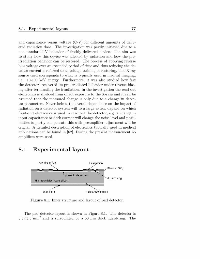
8.1. Experimental layout 77
and capacitance versus voltage (C-V) for different amounts of deliv-ered radiation dose. The investigation was partly initiated due to anon-standard I-V behavior of freshly delivered device. The aim wasto study how this device was affected by radiation and how the pre-irradiation behavior can be restored. The process of applying reversebias voltage over an extended period of time and thus reducing the de-tector current is referred to as voltage training or restoring. The X-raysource used corresponds to what is typically used in medical imaging,i.e. 10-100 keV energy. Furthermore, it was also studied how fastthe detectors recovered its pre-irradiated behavior under reverse bias-ing after terminating the irradiation. In the investigation the read-outelectronics is shielded from direct exposure to the X-rays and it can beassumed that the measured change is only due to a change in detec-tor parameters. Nevertheless, the overall dependence on the impact ofradiation on a detector system will to a large extent depend on whichfront-end electronics is used to read out the detector, e.g. a change ininput capacitance or dark current will change the noise level and possi-bilities to partly compensate this with preamplifier adjustment will becrucial. A detailed description of electronics typically used in medicalapplications can be found in [62]. During the present measurement noamplifiers were used.
8.1 Experimental layout
Figure 8.1: Inner structure and layout of pad detector.
The pad detector layout is shown in Figure 8.1. The detector is3.5×3.5 mm2 and is surrounded by a 50 µm thick guard-ring. The
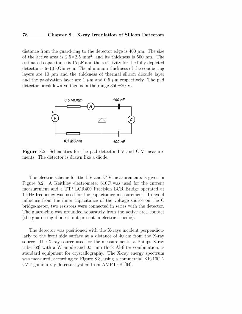
78 Chapter 8. X-ray Irradiation of Silicon Detectors
distance from the guard-ring to the detector edge is 400 µm. The sizeof the active area is 2.5×2.5 mm2, and its thickness is 500 µm. Theestimated capacitance is 15 pF and the resistivity for the fully depleteddetector is 6–10 kOhm·cm. The aluminum thickness of the conductinglayers are 10 µm and the thickness of thermal silicon dioxide layerand the passivation layer are 1 µm and 0.5 µm respectively. The paddetector breakdown voltage is in the range 350±20 V.
Figure 8.2: Schematics for the pad detector I-V and C-V measure-ments. The detector is drawn like a diode.
The electric scheme for the I-V and C-V measurements is given inFigure 8.2. A Keithley electrometer 610C was used for the currentmeasurement and a TTi LCR400 Precision LCR Bridge operated at1 kHz frequency was used for the capacitance measurement. To avoidinfluence from the inner capacitance of the voltage source on the Cbridge-meter, two resistors were connected in series with the detector.The guard-ring was grounded separately from the active area contact(the guard-ring diode is not present in electric scheme).
The detector was positioned with the X-rays incident perpendicu-larly to the front side surface at a distance of 40 cm from the X-raysource. The X-ray source used for the measurements, a Philips X-raytube [63] with a W anode and 0.5 mm thick Al-filter combination, isstandard equipment for crystallography. The X-ray energy spectrumwas measured, according to Figure 8.3, using a commercial XR-100T-CZT gamma ray detector system from AMPTEK [64].
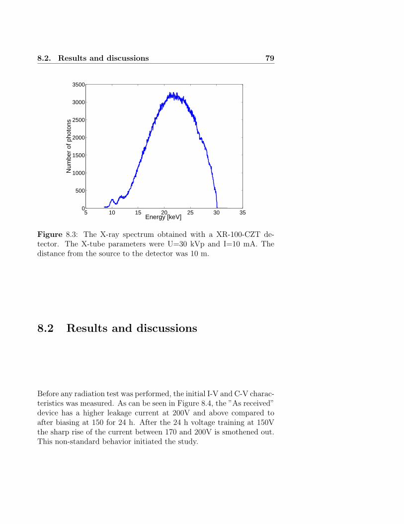
8.2. Results and discussions 79
5 10 15 20 25 30 350
500
1000
1500
2000
2500
3000
3500
Energy [keV]
Num
ber
of p
hoto
ns
Figure 8.3: The X-ray spectrum obtained with a XR-100-CZT de-tector. The X-tube parameters were U=30 kVp and I=10 mA. Thedistance from the source to the detector was 10 m.
8.2 Results and discussions
Before any radiation test was performed, the initial I-V and C-V charac-teristics was measured. As can be seen in Figure 8.4, the ”As received”device has a higher leakage current at 200V and above compared toafter biasing at 150 for 24 h. After the 24 h voltage training at 150Vthe sharp rise of the current between 170 and 200V is smothened out.This non-standard behavior initiated the study.

80 Chapter 8. X-ray Irradiation of Silicon Detectors
0 50 100 150 200 250 300 350
Voltage [V]
Cu
rren
t [A
]
As receivedAfter biasing at 150 V for 24 h
10-10
10-9
10-8
10-7
10-6
10-5
10-4
10-3
Figure 8.4: The I-V curves before irradiation. Errors are within thesize of the markers.
0 50 100 150 200 250 300 350Voltage [V]
Cu
rren
t [A
]
1h Irr. I=10mA150V 24h150V 49h150V 72h150V 96h150V 168h
Infl = 129Ln(t) - 341
0
50
100
150
200
250
300
0 50 100Time [h]
Infl.
poin
t [V
]
10-10
10-9
10-8
10-7
10-6
10-5
10-4
10-3
Figure 8.5: I-V curves obtained after the X-ray irradiation (200 Gy)and indicated hours of voltage training. The subplot shows voltagewhere the sharp leakage current increase occurs as function of timeafter the irradiation. Errors are within the size of the point markers.
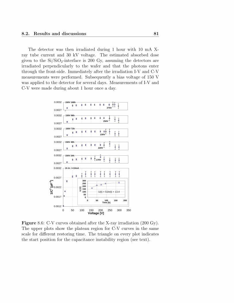
8.2. Results and discussions 81
The detector was then irradiated during 1 hour with 10 mA X-ray tube current and 30 kV voltage. The estimated absorbed dosegiven to the Si/SiO2-interface is 200 Gy, assuming the detectors areirradiated perpendicularly to the wafer and that the photons enterthrough the front-side. Immediately after the irradiation I-V and C-Vmeasurements were performed. Subsequently a bias voltage of 150 Vwas applied to the detector for several days. Measurements of I-V andC-V were made during about 1 hour once a day.
1h Irr. I=10mA
0.0012
0.0017
0.0022
0.0027
0.0032
0 50 100 150 200 250 300 350Voltage [V]
1/C
2 [p
F-2
]
150V 24h
170V
0.0027
0.0032
150V 49h
220V0.0027
0.0032
150V 72h
230V0.0027
0.0032
150V 96h
250V0.0027
0.0032
150V 168h
270V0.0027
0.0032
U(t) = 51ln(t) + 13.4
050
100150200250300
0 50 100 150 200Time [h]
U [
V]
Figure 8.6: C-V curves obtained after the X-ray irradiation (200 Gy).The upper plots show the plateau region for C-V curves in the samescale for different restoring time. The triangle on every plot indicatesthe start position for the capacitance instability region (see text).
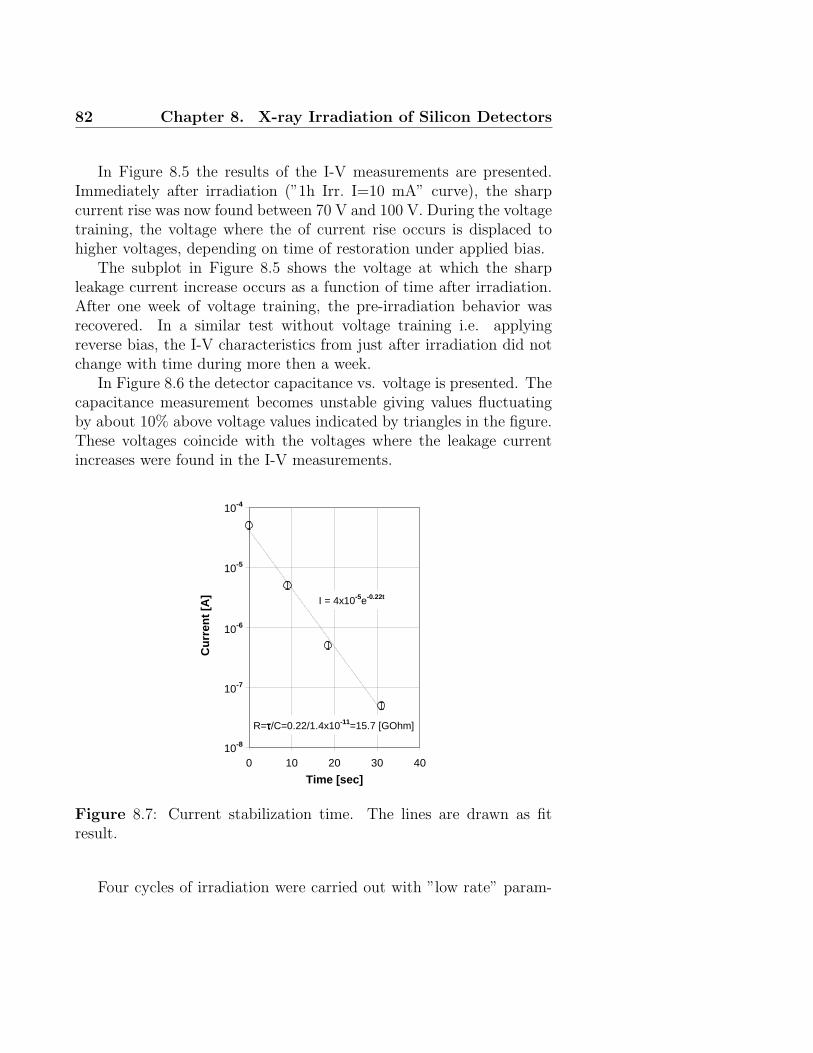
82 Chapter 8. X-ray Irradiation of Silicon Detectors
In Figure 8.5 the results of the I-V measurements are presented.Immediately after irradiation (”1h Irr. I=10 mA” curve), the sharpcurrent rise was now found between 70 V and 100 V. During the voltagetraining, the voltage where the of current rise occurs is displaced tohigher voltages, depending on time of restoration under applied bias.
The subplot in Figure 8.5 shows the voltage at which the sharpleakage current increase occurs as a function of time after irradiation.After one week of voltage training, the pre-irradiation behavior wasrecovered. In a similar test without voltage training i.e. applyingreverse bias, the I-V characteristics from just after irradiation did notchange with time during more then a week.
In Figure 8.6 the detector capacitance vs. voltage is presented. Thecapacitance measurement becomes unstable giving values fluctuatingby about 10% above voltage values indicated by triangles in the figure.These voltages coincide with the voltages where the leakage currentincreases were found in the I-V measurements.
R=ττττ/C=0.22/1.4x10-11=15.7 [GOhm]
I = 4x10⁻⁵e-0.22t
0 10 20 30 40
Time [sec]
Cu
rren
t [A
]
10-8
10-7
10-6
10-5
10-4
Figure 8.7: Current stabilization time. The lines are drawn as fitresult.
Four cycles of irradiation were carried out with ”low rate” param-
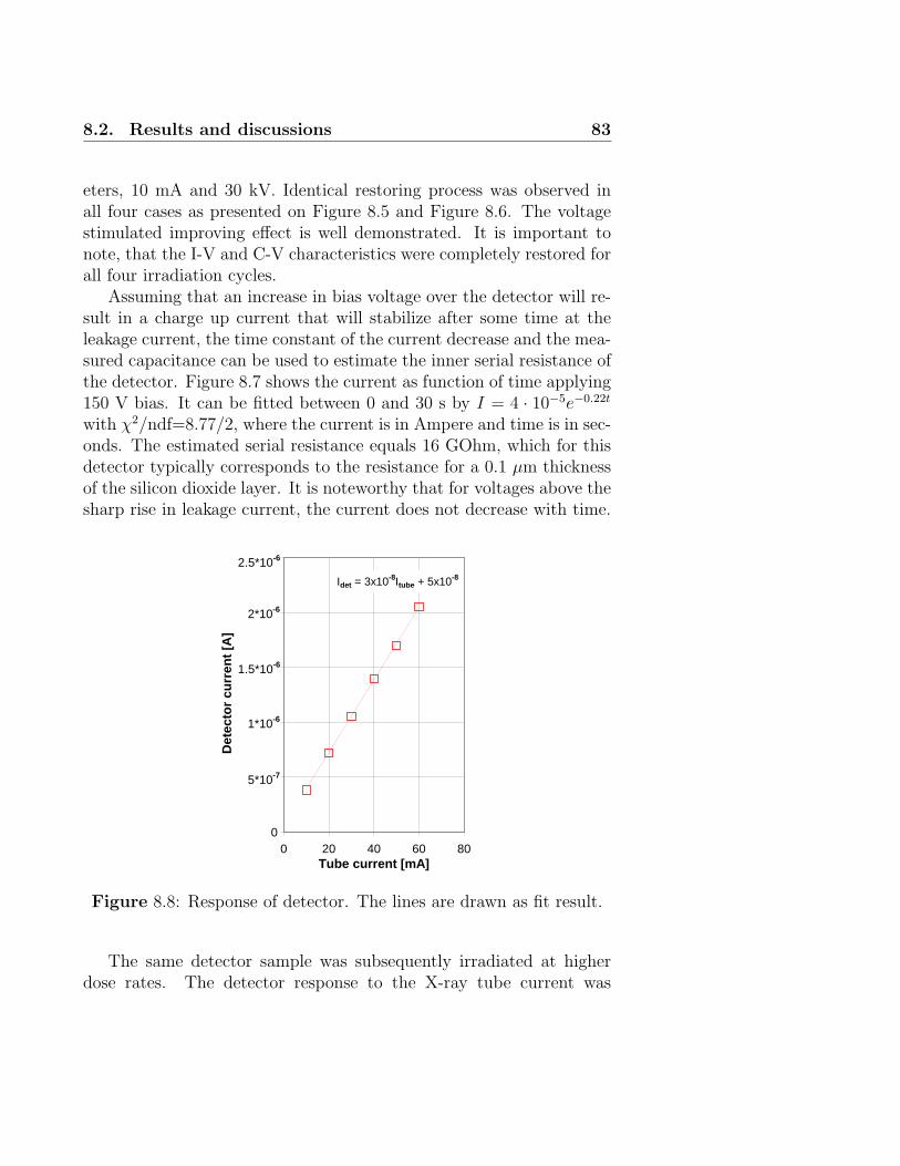
8.2. Results and discussions 83
eters, 10 mA and 30 kV. Identical restoring process was observed inall four cases as presented on Figure 8.5 and Figure 8.6. The voltagestimulated improving effect is well demonstrated. It is important tonote, that the I-V and C-V characteristics were completely restored forall four irradiation cycles.
Assuming that an increase in bias voltage over the detector will re-sult in a charge up current that will stabilize after some time at theleakage current, the time constant of the current decrease and the mea-sured capacitance can be used to estimate the inner serial resistance ofthe detector. Figure 8.7 shows the current as function of time applying150 V bias. It can be fitted between 0 and 30 s by I = 4 · 10−5e−0.22t
with χ2/ndf=8.77/2, where the current is in Ampere and time is in sec-onds. The estimated serial resistance equals 16 GOhm, which for thisdetector typically corresponds to the resistance for a 0.1 µm thicknessof the silicon dioxide layer. It is noteworthy that for voltages above thesharp rise in leakage current, the current does not decrease with time.
Idet = 3x10⁻⁸Itube + 5x10⁻⁸
0 20 40 60 80Tube current [mA]
Det
ecto
r cu
rren
t [A
]
5*10-7
1*10-6
1.5*10-6
2*10-6
2.5*10-6
0
Figure 8.8: Response of detector. The lines are drawn as fit result.
The same detector sample was subsequently irradiated at higherdose rates. The detector response to the X-ray tube current was
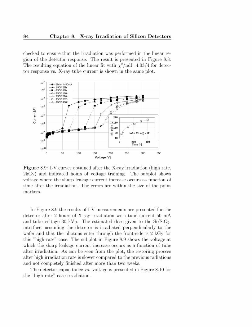
84 Chapter 8. X-ray Irradiation of Silicon Detectors
checked to ensure that the irradiation was performed in the linear re-gion of the detector response. The result is presented in Figure 8.8.The resulting equation of the linear fit with χ2/ndf=4.03/4 for detec-tor response vs. X-ray tube current is shown in the same plot.
0 50 100 150 200 250 300 350
Voltage [V]
Cu
rren
t [A
]
2h Irr. I=50mA150V 26h150V 48h150V 120h150V 210h150V 302h150V 400h
Infl= 51Ln(t) - 121
10
60
110
160
210
0 200 400Time [h]
Infl.
poi
nt [V
]
10-10
10-9
10-8
10-7
10-6
10-5
10-4
10-3
10-2
Figure 8.9: I-V curves obtained after the X-ray irradiation (high rate,2kGy) and indicated hours of voltage training. The subplot showsvoltage where the sharp leakage current increase occurs as function oftime after the irradiation. The errors are within the size of the pointmarkers.
In Figure 8.9 the results of I-V measurements are presented for thedetector after 2 hours of X-ray irradiation with tube current 50 mAand tube voltage 30 kVp. The estimated dose given to the Si/SiO2-interface, assuming the detector is irradiated perpendicularly to thewafer and that the photons enter through the front-side is 2 kGy forthis ”high rate” case. The subplot in Figure 8.9 shows the voltage atwhich the sharp leakage current increase occurs as a function of timeafter irradiation. As can be seen from the plot, the restoring processafter high irradiation rate is slower compared to the previous radiationsand not completely finished after more than two weeks.
The detector capacitance vs. voltage is presented in Figure 8.10 forthe ”high rate” case irradiation.
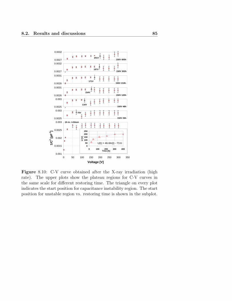
8.2. Results and discussions 85
2h Irr. I=50mA
0.001
0.0015
0.002
0.0025
0.003
0 50 100 150 200 250 300 350
Voltage [V]
1/C
2 [p
F-2
]
150V 26h
70V
0.0025
0.003
150V 48h116V
0.0025
0.003
150V 120h154V
0.0026
0.0031
150V 210h171V
0.0026
0.0031
U(t) = 46.6ln(t) - 73.60
50100150200250
0 100 200 300 400Time [h]
U [
V]
150V 302h197V
0.0027
0.0032
150V 400h201V
0.0027
0.0032
Figure 8.10: C-V curve obtained after the X-ray irradiation (highrate). The upper plots show the plateau regions for C-V curves inthe same scale for different restoring time. The triangle on every plotindicates the start position for capacitance instability region. The startposition for unstable region vs. restoring time is shown in the subplot.
86 Chapter 8. X-ray Irradiation of Silicon Detectors
8.3 Summary
Applying post-irradiation bias voltage to the studied silicon pad detec-tor, produced by Detection Technology [61], has been demonstrated toeffectively restore the basic parameters, thus providing long-term sta-bility in X-ray field. The conclusion from the two different irradiationrate and dose cases is that the degradation effect require more restoringtime under bias for the ”high rate” case.
A detector receiving up to 200 Gy/week should be possible to op-erate provided that it is constantly kept under reverse bias.
Chapter 9
Summary and Outlook
9.1 Comparison with prediction from Lo-
cal Charge Neutrality model
The Local Charge Neutrality (LCN) model permits the estimation ofthe changes in parameters for GaAs compensated by deep level centers.The model [65,66] of hadron induced displacement damage in GaAs wasdeveloped in the Siberian Physical Technical Institute (SPTI) basedon data from hadron irradiation at IHEP and CERN. Local chargeneutrality predicts that acceptor- and donor-like states that appearas a result of displacement damage due to radiation, should respectcharge conservation resulting in a total charge equal to zero. Thereshould thus exist an ”irradiation stable” (LCN) position of the Fermilevel.
From any position of Fermi level in initial material under irradi-ation, the Fermi level shifts to the local charge neutrality level withenergy ELCN . It is also correct for the intrinsic semiconductor mate-rial. In the intrinsic semiconductors the Fermi level is located in themiddle of the band gap Eg. The maximum shift of the Fermi level isequal to Eg/2 − ELCN . This shift equals to 0.17 eV for silicon and0.08 eV for GaAs according to the values of ELCN in these materialsgiven in Table 9.1.
The tendency of increasing resistivity of GaAs under irradiation isdemonstrated in Figure 9.1. The changes in resistivity of the compen-sated GaAs is presented by the line with filled circle data points.
87
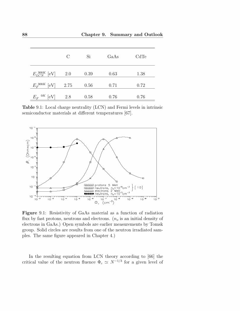
88 Chapter 9. Summary and Outlook
C Si GaAs CdTe
E 300KLCN [eV] 2.0 0.39 0.63 1.38
E 300KF [eV] 2.75 0.56 0.71 0.72
E 0KF [eV] 2.8 0.58 0.76 0.76
Table 9.1: Local charge neutrality (LCN) and Fermi levels in intrinsicsemiconductor materials at different temperatures [67].
Figure 9.1: Resistivity of GaAs material as a function of radiationflux by fast protons, neutrons and electrons. (no is an initial density ofelectrons in GaAs.) Open symbols are earlier measurements by Tomskgroup. Solid circles are results from one of the neutron irradiated sam-ples. The same figure appeared in Chapter 4.)
In the resulting equation from LCN theory according to [66] thecritical value of the neutron fluence Φc ' N−1/3 for a given level of
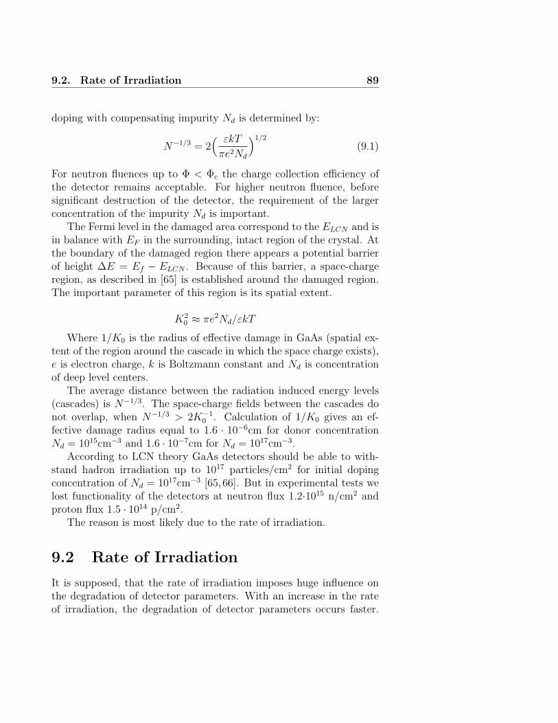
9.2. Rate of Irradiation 89
doping with compensating impurity Nd is determined by:
N−1/3 = 2( εkT
πe2Nd
)1/2
(9.1)
For neutron fluences up to Φ < Φc the charge collection efficiency ofthe detector remains acceptable. For higher neutron fluence, beforesignificant destruction of the detector, the requirement of the largerconcentration of the impurity Nd is important.
The Fermi level in the damaged area correspond to the ELCN and isin balance with EF in the surrounding, intact region of the crystal. Atthe boundary of the damaged region there appears a potential barrierof height ∆E = Ef − ELCN . Because of this barrier, a space-chargeregion, as described in [65] is established around the damaged region.The important parameter of this region is its spatial extent.
K20 ≈ πe2Nd/εkT
Where 1/K0 is the radius of effective damage in GaAs (spatial ex-tent of the region around the cascade in which the space charge exists),e is electron charge, k is Boltzmann constant and Nd is concentrationof deep level centers.
The average distance between the radiation induced energy levels(cascades) is N−1/3. The space-charge fields between the cascades donot overlap, when N−1/3 > 2K−1
0 . Calculation of 1/K0 gives an ef-fective damage radius equal to 1.6 · 10−6cm for donor concentrationNd = 1015cm−3 and 1.6 · 10−7cm for Nd = 1017cm−3.
According to LCN theory GaAs detectors should be able to with-stand hadron irradiation up to 1017 particles/cm2 for initial dopingconcentration of Nd = 1017cm−3 [65, 66]. But in experimental tests welost functionality of the detectors at neutron flux 1.2·1015 n/cm2 andproton flux 1.5 · 1014 p/cm2.
The reason is most likely due to the rate of irradiation.
9.2 Rate of Irradiation
It is supposed, that the rate of irradiation imposes huge influence onthe degradation of detector parameters. With an increase in the rateof irradiation, the degradation of detector parameters occurs faster.
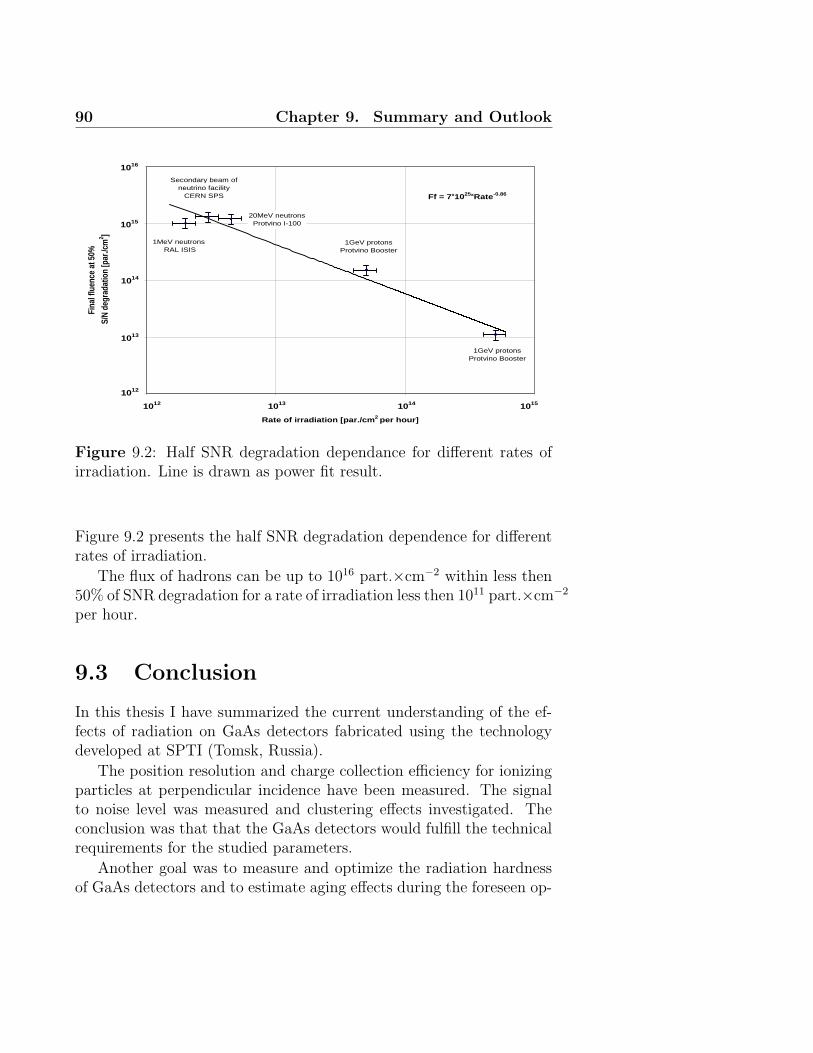
90 Chapter 9. Summary and Outlook
20MeV neutronsProtvino I-100
1GeV protons Protvino Booster
1GeV protons Protvino Booster
1MeV neutrons RAL ISIS
Secondary beam of neutrino facility
CERN SPS Ff = 7x1025xRate-0.86
Rate of irradiation [par./cm2 per hour]
Fina
l flu
ence
at 5
0%
S/N
deg
rada
tion
[par
./cm
2 ]
1012 1013 1014 1015
1012
1013
1014
1015
1016
Figure 9.2: Half SNR degradation dependance for different rates ofirradiation. Line is drawn as power fit result.
Figure 9.2 presents the half SNR degradation dependence for differentrates of irradiation.
The flux of hadrons can be up to 1016 part.×cm−2 within less then50% of SNR degradation for a rate of irradiation less then 1011 part.×cm−2
per hour.
9.3 Conclusion
In this thesis I have summarized the current understanding of the ef-fects of radiation on GaAs detectors fabricated using the technologydeveloped at SPTI (Tomsk, Russia).
The position resolution and charge collection efficiency for ionizingparticles at perpendicular incidence have been measured. The signalto noise level was measured and clustering effects investigated. Theconclusion was that that the GaAs detectors would fulfill the technicalrequirements for the studied parameters.
Another goal was to measure and optimize the radiation hardnessof GaAs detectors and to estimate aging effects during the foreseen op-
9.3. Conclusion 91
eration in a hadron collider. The radiation hardness was estimated byexposing the detectors to gamma, neutron, proton and mixed beamsof short-lived particles leading to a decrease of 20% in the charge-collection efficiency. There is a small increase in the noise due to theirradiation, but the S/N ratio remains above 10 in the worst case ex-pected. No conductivity type inversion has been observed and thedetectors can therefore be operated at room temperature (20oC). Thedata suggest changes in the production of the GaAs compared to in-dustrial production and also in the concentration of compensation im-purities and the thickness of the active layer.
The data suggest that further improvement in performance couldbe expected if the sensitive thickness could be made almost equal tothe physical thickness of the wafer material and if the leakage currentdensity could be reduced.
I believe that GaAs detectors in the future will be a versatile toolin several fields such as medical imaging, non-destructive testing andin physics experiments with high charge multiplicity.
Chapter 10
Acknowledgments
This work could not have been done without the support from severalpeople. I am very grateful for the opportunity given to me by mysupervisors Prof. Per Carlson who took care of my Licentiate. Manythanks go to him for giving support and assistance.
Especially thanks going to Prof. Bengt Lund-Jensen, who was thefinal and a very efficient supervisor, going so deep into all details andaspects of this work, thanks a lot. I would like to thank Prof. Ken-way M. Smith from Physics department of Glasgow University for hisencouragement and guidance in Glasgow and CERN. Many thanks toProf. Stanislav Khludkov and Dr. Oleg Tolbanov for providing re-sources and working environment.
I would like to thank Stefan Rydstrom for very helpful discussion ofexperimental results for semiconductor irradiation and for proof read-ing of thesis.
Finally, I am grateful to all my colleagues and friends from Protvino,Glasgow and Stockholm groups for providing such great and friendlywork-places.
92
Bibliography
[1] Czochralski crystal-growth system. NASA Tech Briefs, 21:p10,1997.
[2] C.R.Wie. Crystal Viewer. http://jas.eng.buffalo.edu/education/solid/unitCell/home.html, Copyright 1997-1998.
[3] Z. Naturforsch H. Welker. Vol.A, No.7:p.774, 1952.
[4] J. Blakemore. Semiconducting and Other Major Properties ofGallium Arsenide. J. Appl. Phys., Vol.53, No.10, 1982.
[5] Sammy Kayali. GaAs Material Properties. JPL Publication 96-25,December 15, 1996.
[6] S. M. Sze. Semiconductor Devices Physics and Technology. J.Wiley, New York, 1985.
[7] R. F. Pierret. Semiconductor Fundamentals. Addison-Wesley Pub-lishing, New York, 1989.
[8] R. Williams. Modern GaAs Processing Methods. Artech House,Dedham, MA, 1990.
[9] Y. Nanishi. J. Appl. Phys., Vol.22, 1983.
[10] S. Miyazawa. Appl. Phys. Lett., Vol.44, 1984.
[11] T. Honda. J. Appl. Phys., Vol.22, 1983.
[12] H. C. Casey. Diffusion in III-V Compound Semiconductors.Atomic Diffusion in Semiconductors, D. Shaw, Editor, Plenum,New York, 1973.
93
94 Bibliography
[13] S. Y. Chiang. Properties of Vacancy Defects in GaAs Single Crys-tals. J. Appl. Phys., Vol.45:p.2986, 1975.
[14] S. Markram-Ebied. Nature of EL2: The Main Native MidgapElectron Trap in VPE and Bulk GaAs. Semi-insulating III-V Ma-terials, D. Look, Editor, Shiva Publishing Ltd., England, 1984.
[15] Tolbanov O.P. et al. I-V characteristics of gallium-arsenideπ–ν–n structures, doped with Fe and Cr, in strong electricalfields range. Semiconductor physics and technology., Vol.20,No.11:p.2072, 1985.
[16] Khludkov S.S. GaAs shower S-diodes. Izvestiya vuzov SSSR,Fizika, Vol. 26, No. 10:p.67 (in Russian), 1983.
[17] Gaman V.I. C-V characteristics of diode structures based on theGaAs, compensated by Mn and Fe. Izvestiya vuzov SSSR, Fizika.,v.26, No.10:p.79 (in Russian), 1983.
[18] Chmill V.B. et. al. An exploration of GaAs structures for solid-state detectors. Nucl. Instr. and Meth., A326:p.310, 1993.
[19] Chmill V.B. et. al. Exploration of GaAs structures with π-ν junc-tion for coordinate sensitive detectors. Nucl. Instr. and Meth.,A340:pp.328–340, 1994.
[20] Chmill V.B. et al. Radiation hard microstrip detectors based ongallium arsenide. Nucl. Instr. and Meth., A379:pp.406–408, 1996.
[21] Chmill V.B. et al. Radiation resistanse of GaAs structures. ATLASInner detector note no.143, 1995.
[22] Chmill V.B. et al. Particle detector based on GaAs. Radia-tion hardness and spatial resolution. Nucl. Instr. and Meth., A409:pp.247–250, 1998.
[23] Chmill V.B. et al. The Result of GaAs Irradiation at Mixed BeamNeutrino Cave CERN. Fifth International Workshop on GalliumArsenide Detectors and Related Compounds (Cividale del Friuli,Italy June17-20 1997) Nucl. Instr. and Meth., A 410:pp.54–60,1998.
Bibliography 95
[24] V.Chmill et al. Investigation of epitaxial GaAs charged particledetectors. Nucl. Instr. and Meth., A438, Number 2:pp.362–367,December 1999.
[25] V.Chmill. X-ray Irradiation of Silicon Detectors. Nucl. Instr. andMeth., A:submitted, 2006.
[26] R.E. Kremer et al. Low dislocation density GaAs grown bythe bridgman technique. Journal of Material Research, Vol.5,No.7.:1468, 1996.
[27] Golovin V.M. et al. Hybrid low-noise amplifier with bipolar tran-sistors. Preprint IHEP 89-231. Protvino, Russia,, 1989.
[28] Vorobiev A.P. et.al. Searching gallium arsenide structures for co-ordinate sensitive detectors. Preprint IHEP 91- 192. Protvino,Russia, 1991.
[29] Demeester G.B. Ramanamurthy P.V. Nucl. Instr. and Meth.,A56:p.93, 1967.
[30] Akimov Yu.K. et al. Semiconductor detectors in experimentalphysics. Energoatomizdat, Moscow, 1989.
[31] Tove P.A. Seibt W., Sundstrom K.E. Nucl. Instr. and Meth.,A113:pp.317–324, 1973.
[32] Chmill V.B. et al. Exploration of GaAs structures for solid-statedetectors. Preprint IHEP 92-59, Protvino, Russia,, (Submitted toNIM). NIM A326:pp.310–312, 1993.
[33] Schoklye. Van Roosbroeck W. Problems of semiconductor physics.Moscow, (in Russian), 1958.
[34] Van Roosbroeck W. Physycs Revew, V.91:p.282, 1953.
[35] Keldysh L.V. Physics of Semiconductors. ZhTEF (in russian),Vol.34:p.1138, 1958.
[36] Bertin R. et al. Nucl. Instr. and Meth., A294:P.211, 1990.
[37] Beaumont S. et al. CERN/DRDC/90-58,, page DRDC/P13, 1990.
96 Bibliography
[38] Beaumont S. et al. Gallium arsenide microstrip detectors forcharged particles. CERN–PRE/92-51, 1992.
[39] Beaumont S. et al. Gallium arsenide microstrip detectors. NuclearPhysycs, B23A:pp.417–418, 1991.
[40] Jeong M.U. et. al. Radiation Effects in Semiconductors. Gordonand Breac Publish. N.Y., page p.287, 1971.
[41] Aukerman L.W. Semiconductors and Semimetals. N.Y.AcodemicPress ed. R.K. Willardson and A.C. Beer., V.4, 1968.
[42] Coates R. and Mitchell E.W.J. Adv. Physics, V.24:p.593, 1975.
[43] Lang D.V. Inst. Phys. Conf. Ser., n31:p.70, 1977.
[44] Brudnyi V.N. et. al. Solid State Comm., V.34:pp.117–119 Perga-mon Press Ltd., 1980.
[45] Krivov M.A. Brudnyi V.N. Radiations Damage in Gallium Ar-senide. Izvestia VUZ, N1(212):(in Russian), 1980.
[46] Logan R.A. Lang D.V. Radiation effects in semiconductors. J.Appl. Phys., V47:p.3587, 1987.
[47] V.M. Golovin et. al. Hybrid low-noise amplifier with bipolar tran-sistors. Preprint IHEP 89-231, Protvino:Russia, 1989.
[48] M.Bruzzi. GaAs Detectors and Related Compaunds. Proceed-ing of the International Workshop(1997) Nucl. Instr. and Meth.,A395:pp.1–151, 1997.
[49] J.E. Eberhardt et al. . Nucl. Instr. and Meth., A395:pp.463–476,1971.
[50] P.E.Gibbons and J.H.Howes. . IEEE Trans. Nucl. Sci., NS-19(3):p.353, 1972.
[51] K.Hesse et al. . Nucl. Instr. and Meth., 101:p.39, 1972.
[52] Kobayashi et al. . IEEE Trans. Nucl. Sci., NS-19(3):p.324, 1972.
[53] Kobayashi et al. . IEEE Trans. Nucl. Sci., NS-20(1):p.310, 1973.
Bibliography 97
[54] Shockley W. Sah C.T., Noyce R.N. . Proc. IEEE, 45:p.1228, 1957.
[55] S.M. Sze. Physics of Semiconductor Devices. Wiley, New York,1983.
[56] M.Bruzzi. Material engineering for the development of ultra-radiation hard semiconductor detectors. Nucl. Instr. and Meth.,A518:pp.336–337, 2004.
[57] R. Rando et al. A. Candelori, D. Bisello. Radiation hardness ofsilicon detectors for high-energy physics applications. IEEE Trans.Nucl. Sci., vol.50:pp.1121 –1128, 2003.
[58] P. Rappoport J. Loferski. . Phys. Rev. III, page pp. 32, 1958.
[59] R. Bauerlein. . Zs. Phys., 176 (4):pp. 498, 1963.
[60] Z. Marka et al. . J. Appl. Phys., Vol.93:No.4, 15 February 2003.
[61] Detection Technology web site. http://www.deetee.com.
[62] John Yorkston. Digital Radiographic Technology. Advances inDigital Radiography:, RSNA Categorical Course in Diagnostic Ra-diology Physics:pp 2336, 2003.
[63] Philips X ray system. PW1830/00/25/26/40. HT Generator In-struction Manual.
[64] Amptek Inc. company web site. http://www.amptek.com.
[65] S.S. Khludkov et. al. Proton-induced displacement damage inGaAs and radiation hardness of semiconductor detectors for highenergy physics. Nucl. Instr. and Meth., A395:pp.60–64, 1997.
[66] S.S. Khludkov et. al. Radiation hardness of semiconductor detec-tors for high-energy physics. J. Phys. D:Appl. Phys., 29:pp.1559–1563, 1996.
[67] C. Kittel. Introduction to solid state physics. 6th Ed., New York:John Wiley:p.185, 1986.
List of Figures
1.1 Unit cube of GaAs crystal lattice. . . . . . . . . . . . . 5
1.2 Energy band diagram for GaAs. . . . . . . . . . . . . . 6
1.3 Energy band structure of GaAs. . . . . . . . . . . . . . 7
1.4 Energy band diagram of GaAs with impurities. . . . . 10
2.1 Distribution of shallow donors, acceptors, deep accep-tors. Energy diagram . . . . . . . . . . . . . . . . . . . 15
2.2 Energy zone diagrams. . . . . . . . . . . . . . . . . . . 17
3.1 Forward and reverse I-V branch of the samples. . . . . 20
3.2 Spectra of the signals from p-π-ν-n structure registeredin the charge sensitive channel for different bias voltage. 22
3.3 C–V of the p-π-ν-n sample (at the frequency 1 MHz). . 23
3.4 Spectrum of the signals from the n+-π-ν-n structure,exposed to 2 MeV β–particles . . . . . . . . . . . . . . 23
3.5 Spectrum of the signals from the n+-π-ν-n sample ex-posed to radioactive 241Am α–particles, registered in thecharge sensitive channel. . . . . . . . . . . . . . . . . . 24
3.6 Estimated dependence of the charge collection time tak-ing into account the plasma effect for the release of 50000electrons. . . . . . . . . . . . . . . . . . . . . . . . . . 27
3.7 Estimated dependence of the charge collection time tak-ing into account the plasma effect at the integrated po-tential difference 50 mV as function of the numbers ofinjected electron. . . . . . . . . . . . . . . . . . . . . . 27
3.8 The charge spectra of the signals from the p-π-ν-n sam-ple exposed to monoenergetic 0.6 MeV β–particles atvarious bias voltages. . . . . . . . . . . . . . . . . . . . 28
98
List of Figures 99
3.9 The charge spectra of the signals from the p-π-ν-n sam-ple irradiated by 2 MeV monoenergetic β–particles atdifferent bias voltages. . . . . . . . . . . . . . . . . . . 29
3.10 The charge spectrum of the signals from p-π-ν-n samplesirradiated with 2 MeV by β–particles, registered in thecurrent sensitive channel at 100 V bias. . . . . . . . . . 30
3.11 The temperature dependence of the noise in GaAs samples. 32
3.12 Temperature dependence of the signal peak position inGaAs samples. . . . . . . . . . . . . . . . . . . . . . . . 33
3.13 The signal-to-noise ratio vs. temperature in GaAs samples. 33
3.14 The noise of GaAs samples vs. absorbed dose of 137Csγ-rays for two different samples. . . . . . . . . . . . . . 34
3.15 The signal peak position vs. absorbed dose of 137Cs γ-rays for two different samples. . . . . . . . . . . . . . . 35
3.16 The SNR vs. absorbed dose of 137Cs γ-rays for two dif-ferent samples. . . . . . . . . . . . . . . . . . . . . . . 35
4.1 Resistivity of GaAs material as a function of radiationflux by fast protons, neutrons and electrons. . . . . . . 39
4.2 Forward I–V characteristic as a function of neutron ir-radiation. . . . . . . . . . . . . . . . . . . . . . . . . . 40
4.3 Reverse I–V characteristic as a function of neutron irra-diation. . . . . . . . . . . . . . . . . . . . . . . . . . . 41
4.4 Resistivity of the π–layer vs. neutron irradiation (left).Photovoltaic e.m.f. vs. neutron irradiation (right). Flu-ence scale from 1011 to 1016 n/cm2, ρ-scale from 104 to109 Ohm·cm and Uo from 10−3 to 1 V. . . . . . . . . . 42
4.5 C–V variations as a function of bias for different neutronirradiation. . . . . . . . . . . . . . . . . . . . . . . . . 43
4.6 Noise (RMS) vs. neutron irradiation. . . . . . . . . . . 44
4.7 Charge collection (spectrum peak position for most prob-able energy loss) vs. neutron irradiation. . . . . . . . . 45
4.8 Signal to noise ratio vs. neutron irradiation. . . . . . . 45
5.1 Signal response vs. muon fluence. . . . . . . . . . . . . 50
5.2 Signal response vs. bias voltage. . . . . . . . . . . . . . 51
5.3 Experimental layout. . . . . . . . . . . . . . . . . . . . 52
5.4 Raw data from one of the detectors and the BCT counter. 53
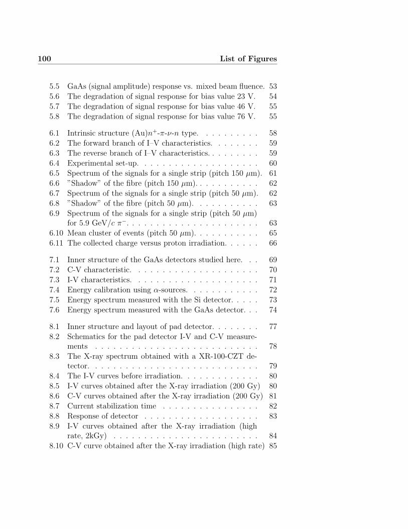
100 List of Figures
5.5 GaAs (signal amplitude) response vs. mixed beam fluence. 53
5.6 The degradation of signal response for bias value 23 V. 54
5.7 The degradation of signal response for bias value 46 V. 55
5.8 The degradation of signal response for bias value 76 V. 55
6.1 Intrinsic structure (Au)n+-π-ν-n type. . . . . . . . . . 58
6.2 The forward branch of I–V characteristics. . . . . . . . 59
6.3 The reverse branch of I–V characteristics. . . . . . . . . 59
6.4 Experimental set-up. . . . . . . . . . . . . . . . . . . . 60
6.5 Spectrum of the signals for a single strip (pitch 150 µm). 61
6.6 ”Shadow” of the fibre (pitch 150 µm). . . . . . . . . . . 62
6.7 Spectrum of the signals for a single strip (pitch 50 µm). 62
6.8 ”Shadow” of the fibre (pitch 50 µm). . . . . . . . . . . 63
6.9 Spectrum of the signals for a single strip (pitch 50 µm)for 5.9 GeV/c π−. . . . . . . . . . . . . . . . . . . . . . 63
6.10 Mean cluster of events (pitch 50 µm). . . . . . . . . . . 65
6.11 The collected charge versus proton irradiation. . . . . . 66
7.1 Inner structure of the GaAs detectors studied here. . . 69
7.2 C-V characteristic. . . . . . . . . . . . . . . . . . . . . 70
7.3 I-V characteristics. . . . . . . . . . . . . . . . . . . . . 71
7.4 Energy calibration using α-sources. . . . . . . . . . . . 72
7.5 Energy spectrum measured with the Si detector. . . . . 73
7.6 Energy spectrum measured with the GaAs detector. . . 74
8.1 Inner structure and layout of pad detector. . . . . . . . 77
8.2 Schematics for the pad detector I-V and C-V measure-ments . . . . . . . . . . . . . . . . . . . . . . . . . . . 78
8.3 The X-ray spectrum obtained with a XR-100-CZT de-tector. . . . . . . . . . . . . . . . . . . . . . . . . . . . 79
8.4 The I-V curves before irradiation. . . . . . . . . . . . . 80
8.5 I-V curves obtained after the X-ray irradiation (200 Gy) 80
8.6 C-V curves obtained after the X-ray irradiation (200 Gy) 81
8.7 Current stabilization time . . . . . . . . . . . . . . . . 82
8.8 Response of detector . . . . . . . . . . . . . . . . . . . 83
8.9 I-V curves obtained after the X-ray irradiation (highrate, 2kGy) . . . . . . . . . . . . . . . . . . . . . . . . 84
8.10 C-V curve obtained after the X-ray irradiation (high rate) 85
List of Figures 101
9.1 Resistivity GaAs samples as a function of radiation fluxby fast protons, neutrons and electrons. . . . . . . . . . 88
9.2 Half SNR degradation dependance for different rates ofirradiation. . . . . . . . . . . . . . . . . . . . . . . . . 90
List of Tables
1.1 Room-temperature properties of GaAs and Si. . . . . . 6
2.1 Type of tested GaAs detectors . . . . . . . . . . . . . . 18
4.1 Parameters of the I-100 proton beam. . . . . . . . . . . 384.2 Main characteristics of the irradiation volume. . . . . . 38
5.1 Summary results of hadron beam irradiation. The linesbefore the last is preceding measurements and was doneon other facilities. . . . . . . . . . . . . . . . . . . . . 49
6.1 Cluster probability for 50 µm and 150 µm pitch detectors. 646.2 Most probable collected charge from detector and SNR
for GaAs detectors after neutron irradiation at RAL. . 66
7.1 Results for the Si and GaAs detectors obtained from theα-spectrum measurements. . . . . . . . . . . . . . . . . 74
9.1 Local charge neutrality (LCN) and Fermi levels in in-trinsic semiconductor materials. . . . . . . . . . . . . . 88
102