Properties of Solids Electrical Resistivity
27
Manuel Núñez Regueiro Properties of Solids Electrical Resistivity
Transcript of Properties of Solids Electrical Resistivity
Manuel Núñez Regueiro
Properties of Solids
Electrical Resistivity
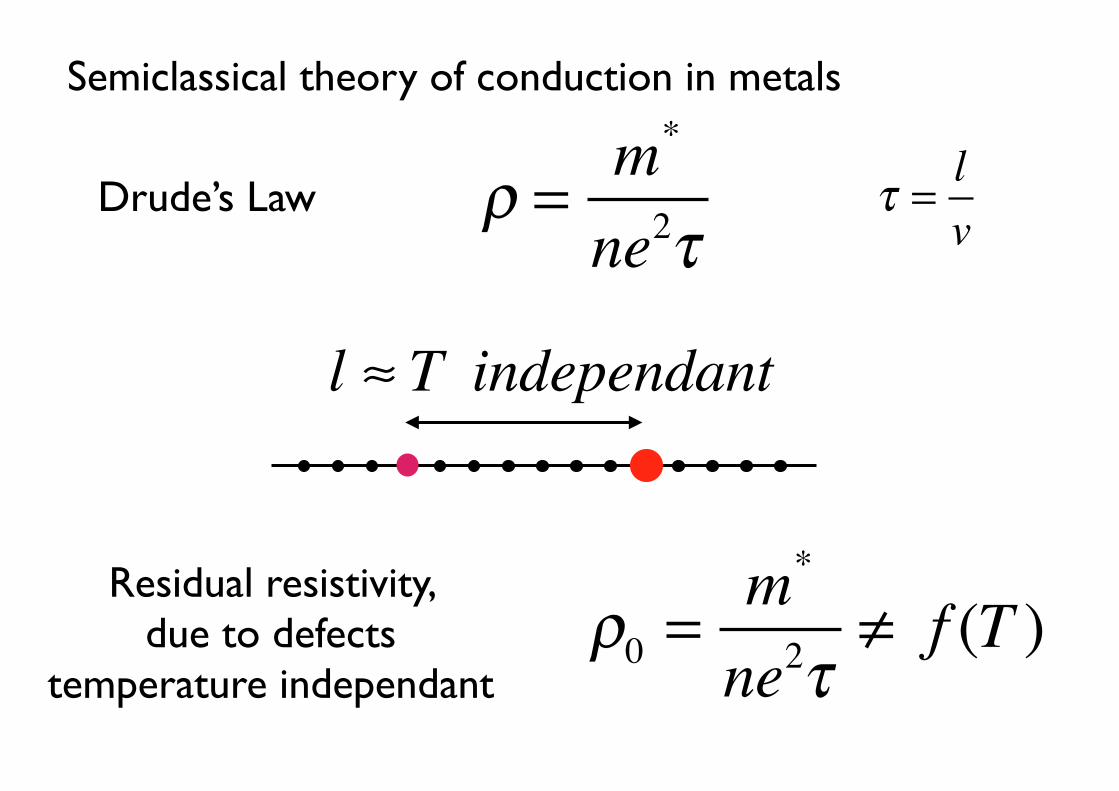
Semiclassical theory of conduction in metals
Drude’s Law ρ =m*
ne2ττ =
lv
l ≈ T independant
ρ0 =m*
ne2τ≠ f (T )
Residual resistivity, due to defects
temperature independant
0
0,2
0,4
0,6
0,8
1
1,2
0 50 100 150 200 250
Elec
tric
al r
esist
ance
(Ω)
Temperature (K)
R α T
R α T 5
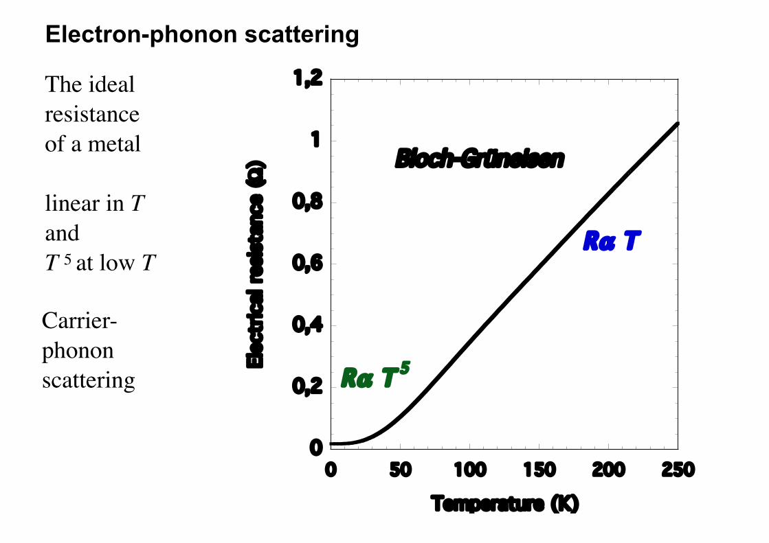
Bloch-Grüneisen
The idealresistanceof a metal
linear in TandT 5 at low T
Carrier-phonon scattering
Electron-phonon scattering
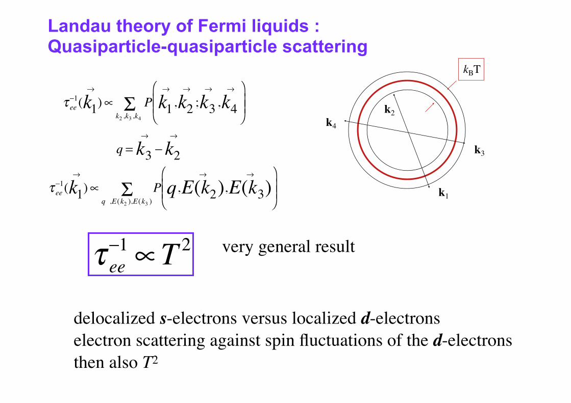
kBT
k2
k3
k1
k4
�
τ ee−1(
→
k1)∝k2 ,k3 ,k4Σ P
→
k1,→
k2 ;→
k3 ,→
k4⎛
⎝ ⎜ ⎜
⎞
⎠ ⎟ ⎟
�
τ ee−1(
→
k1)∝q ,E(k2 ),E(k3 )Σ P q,
→
E(k2),→
E(k3)⎛
⎝ ⎜ ⎜
⎞
⎠ ⎟ ⎟
�
τ ee−1∝T 2
delocalized s-electrons versus localized d-electronselectron scattering against spin fluctuations of the d-electronsthen also T2
�
�
q =→
k3 −→
k2
Landau theory of Fermi liquids : Quasiparticle-quasiparticle scattering
very general result
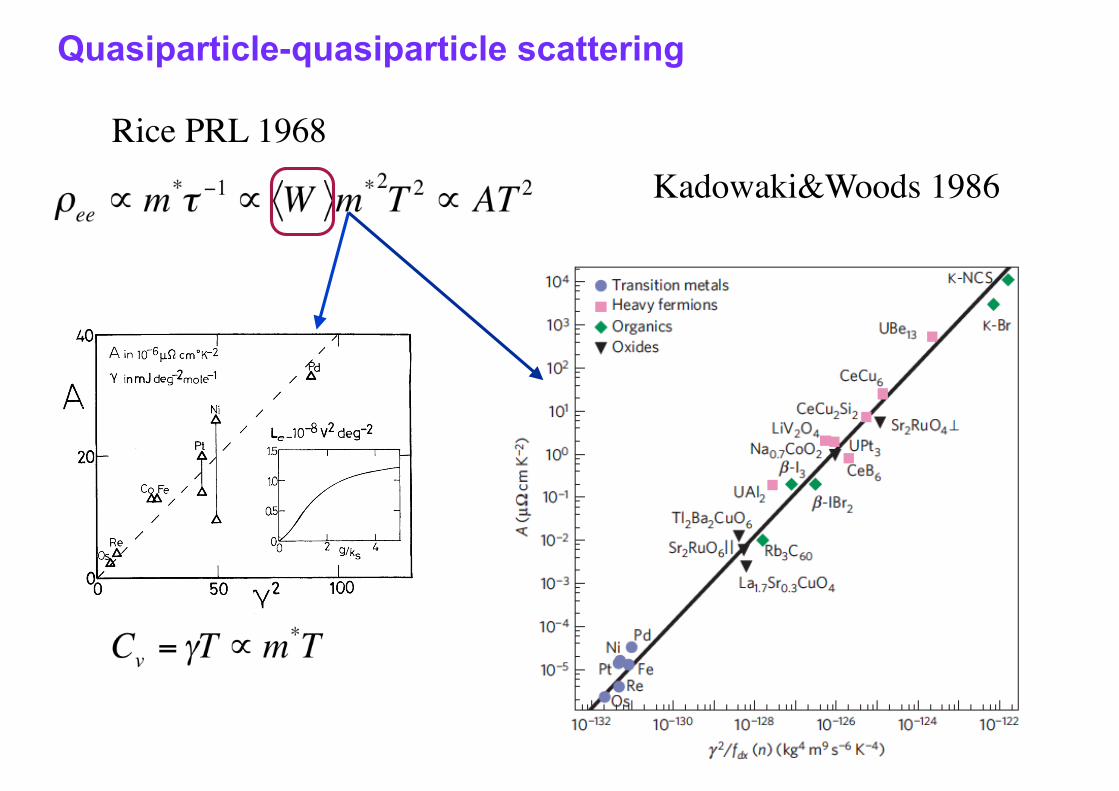
5
Rice PRL 1968Kadowaki&Woods 1986
Quasiparticle-quasiparticle scattering
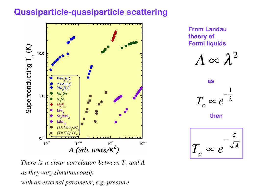
There is a clear correlation between Tc and A as they vary simultaneously with an external parameter, e.g. pressure
Quasiparticle-quasiparticle scattering
Tc ∝ e−
ςA
From Landau theory ofFermi liquids
A ∝ λ2
Tc ∝ e−1λ
as
then
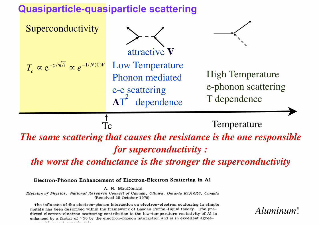
Aluminum!
High Temperaturee-phonon scatteringT dependence
attractive V
Temperature
Low TemperaturePhonon mediatede-e scatteringAT dependence2
Superconductivity
TcThe same scattering that causes the resistance is the one responsible
for superconductivity :the worst the conductance is the stronger the superconductivity
Quasiparticle-quasiparticle scattering
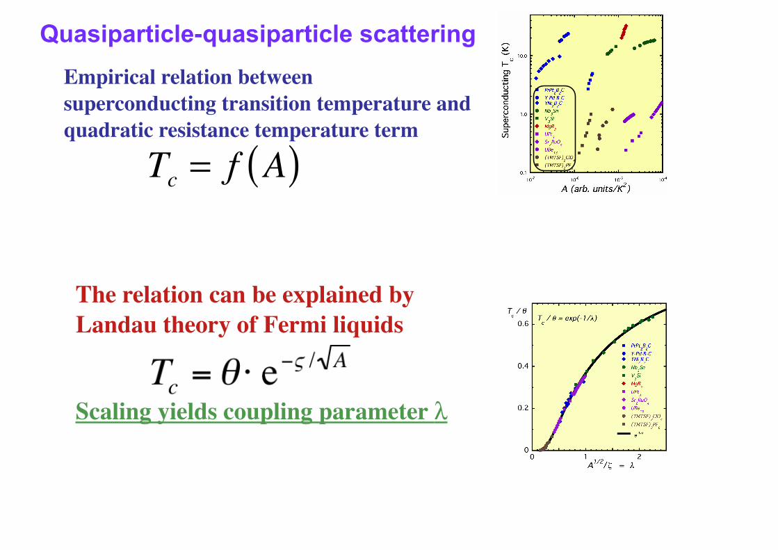
Empirical relation betweensuperconducting transition temperature andquadratic resistance temperature term
The relation can be explained byLandau theory of Fermi liquids
Scaling yields coupling parameter λ
Tc = f A( )
Quasiparticle-quasiparticle scattering
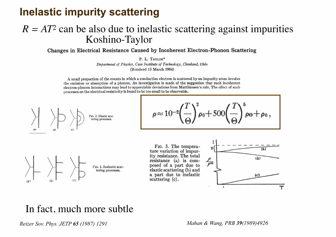
Inelastic impurity scattering R = AT2 can be also due to inelastic scattering against impurities
Koshino-Taylor
In fact, much more subtleMahan & Wang, PRB 39(1989)4926Reizer Sov. Phys. JETP 65 (1987) 1291
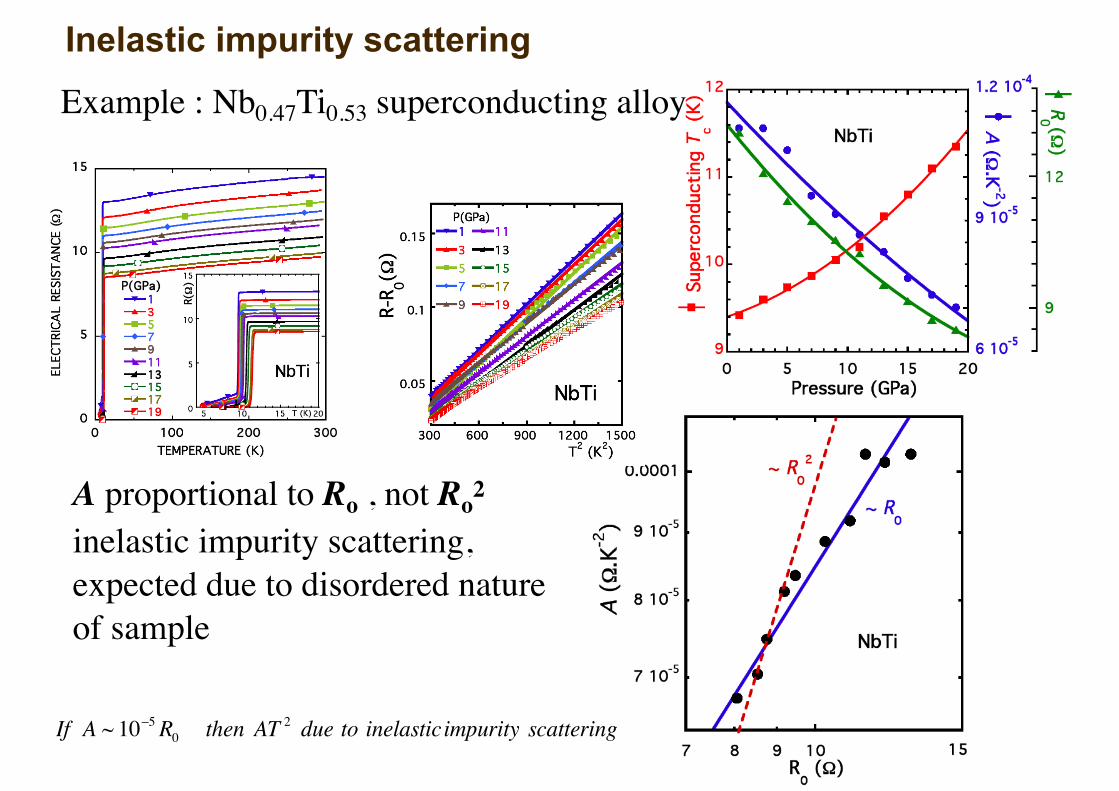
Example : Nb0.47Ti0.53 superconducting alloy
A proportional to Ro , not Ro2
inelastic impurity scattering, expected due to disordered natureof sample
If A ~ 10−5R0 then AT2 due to inelasticimpurity scattering
Inelastic impurity scattering
0
0.2
0.4
0.6
0.8
1
1
0 50 100 150 200 250 300
Δ
Temperature
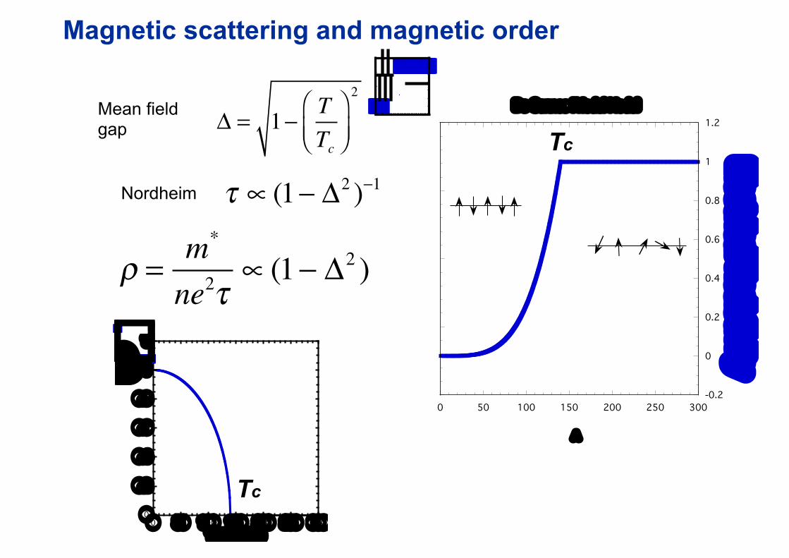
Δ = 1− TTc
⎛⎝⎜
⎞⎠⎟
2Mean field gap
τ ∝ (1− Δ2 )−1Nordheim
ρ =m*
ne2τ∝ (1− Δ2 )
Magnetic scattering and magnetic order
-0.2
0
0.2
0.4
0.6
0.8
1
1.2
0 50 100 150 200 250 300
De Gennes Friedel Model
Electrical Resistivity
A
Tc
Tc
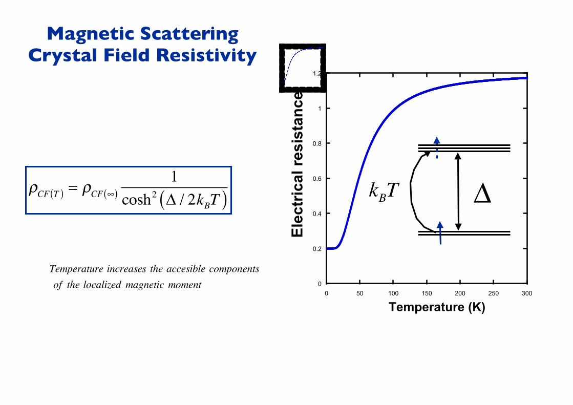
ρCF T( ) = ρCF ∞( )1
cosh2 Δ / 2kBT( )
Magnetic ScatteringCrystal Field Resistivity
Temperature increases the accesible components of the localized magnetic moment
ΔkBT
0
0.2
0.4
0.6
0.8
1
1.2
0 50 100 150 200 250 300El
ectr
ical
resi
stan
ceTemperature (K)
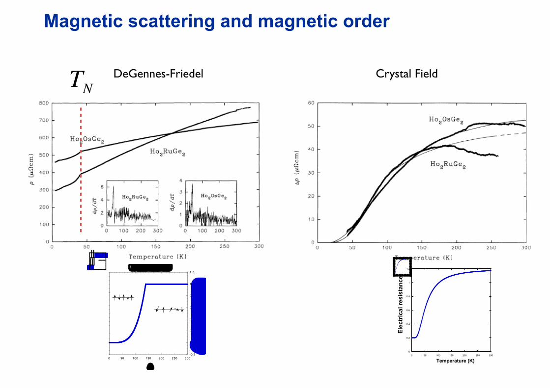
TN DeGennes-Friedel Crystal Field
Magnetic scattering and magnetic order
0
0.2
0.4
0.6
0.8
1
1.2
0 50 100 150 200 250 300
Elec
tric
al re
sist
ance
Temperature (K)-0.2
0
0.2
0.4
0.6
0.8
1
1.2
0 50 100 150 200 250 300
De Gennes Friedel Model
Electrical Resistivity
A
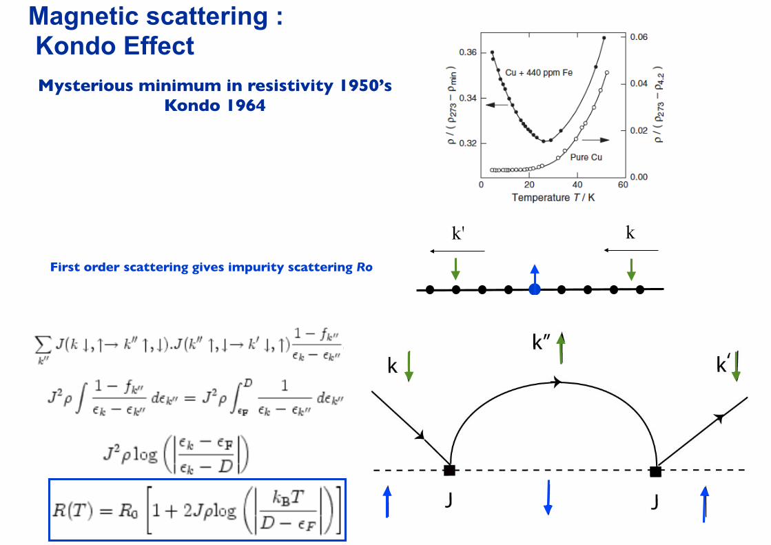
Magnetic scattering : Kondo Effect
kk'First order scattering gives impurity scattering Ro
Mysterious minimum in resistivity 1950’sKondo 1964
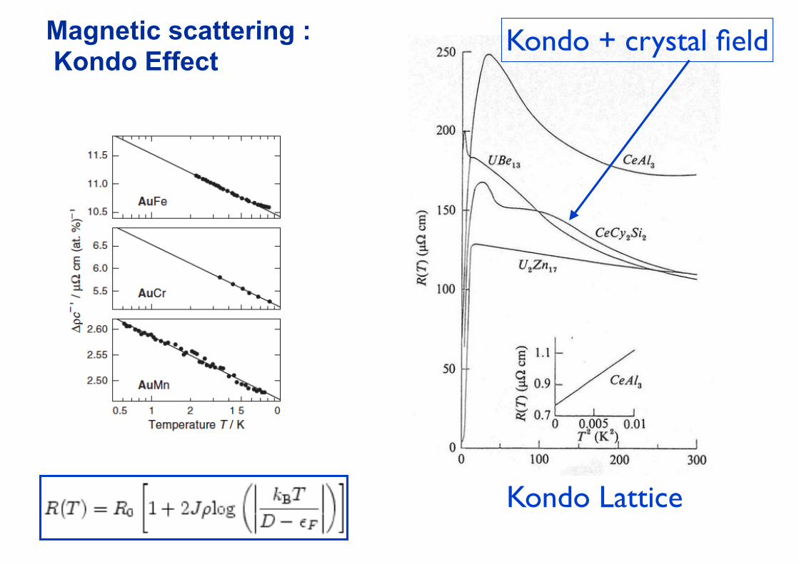
Magnetic scattering : Kondo Effect
Kondo Lattice
Kondo + crystal field
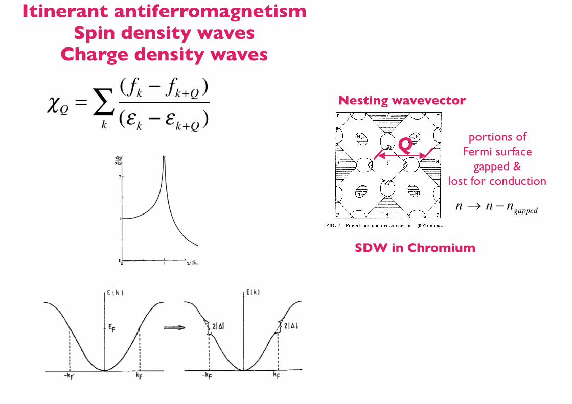
Itinerant antiferromagnetismSpin density waves
Charge density waves
Nesting wavevector
portions of Fermi surface
gapped & lost for conduction
n → n − ngapped
SDW in Chromium
Q
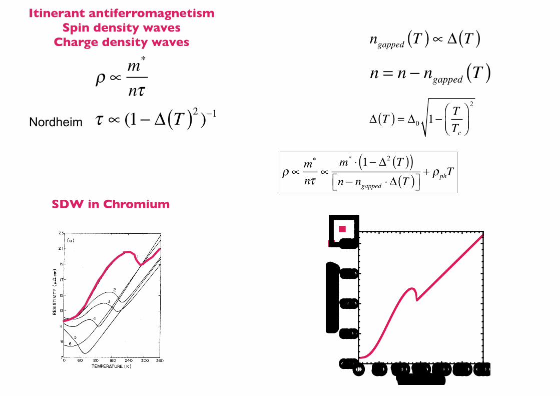
ρ ∝m*
nττ ∝ (1− Δ T( )2 )−1Nordheim
Itinerant antiferromagnetismSpin density waves
Charge density waves ngapped T( )∝ Δ T( )
n = n − ngapped T( )
ρ ∝m*
nτ∝
m* ⋅ 1− Δ2 T( )( )n − ngapped ⋅ Δ T( )⎡⎣ ⎤⎦
+ ρphT
Δ T( ) = Δ0 1− TTc
⎛⎝⎜
⎞⎠⎟
2
SDW in Chromium
0.000
50.00
100.0
150.0
200.0
0 50 100 150 200 250 300
Elec
tric
al R
esist
ivity
Temperature
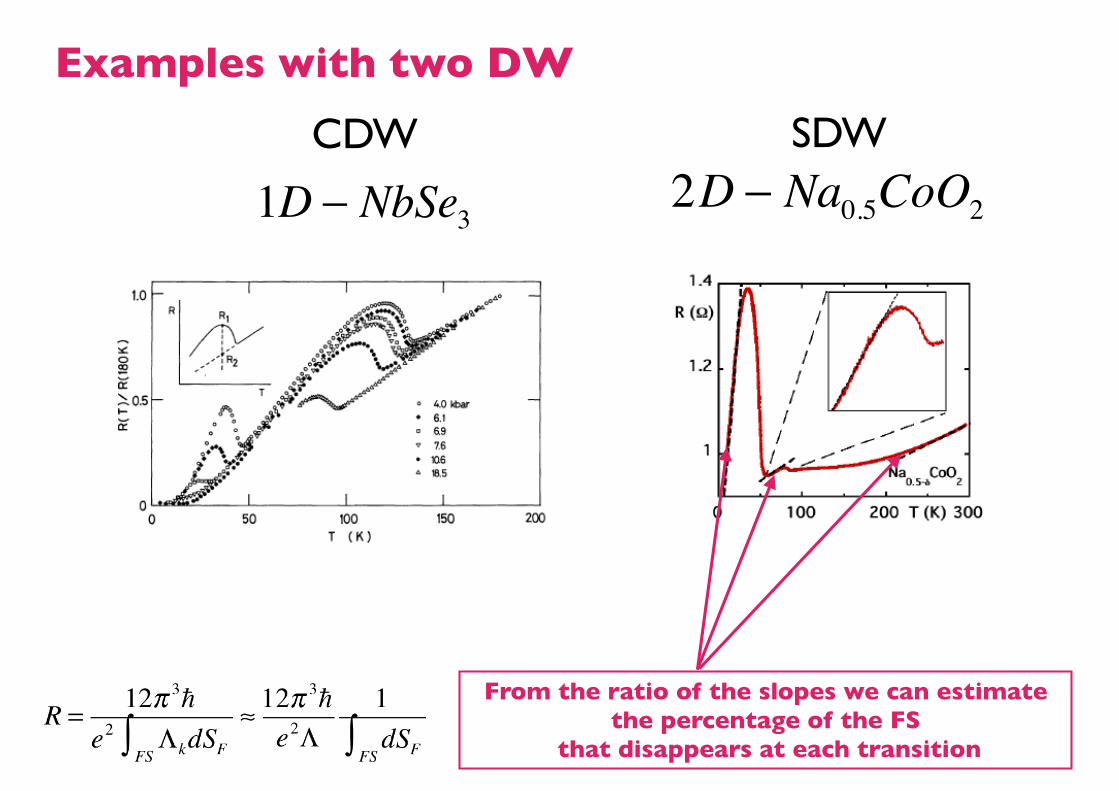
1D − NbSe3 2D − Na0.5CoO2
CDW SDW
Examples with two DW
From the ratio of the slopes we can estimate the percentage of the FS
that disappears at each transition
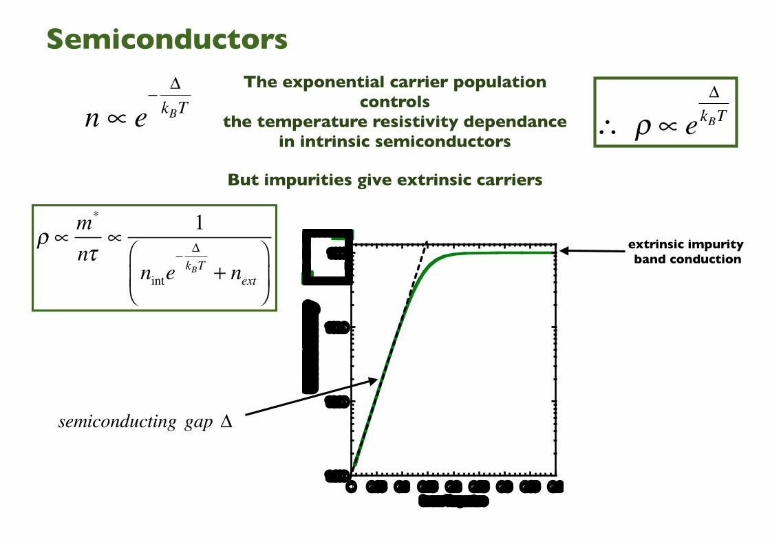
Semiconductors
ρ ∝m*
nτ∝
1
ninte−
ΔkBT + next
⎛
⎝⎜
⎞
⎠⎟
n ∝ e−
ΔkBT
The exponential carrier population controls
the temperature resistivity dependancein intrinsic semiconductors
∴ ρ ∝ eΔkBT
extrinsic impurity band conduction
But impurities give extrinsic carriers
semiconducting gap Δ
1.000
10.00
100.0
1000
0 0.05 0.1 0.15 0.2 0.25 0.3 0.35 0.4
Elec
tric
la re
sistiv
ity
Inverse Temperature
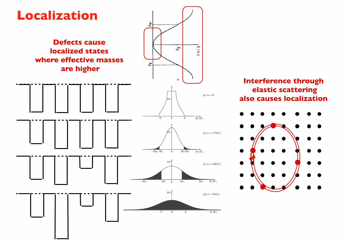
Localization
Defects cause localized states
where effective masses are higher
Interference through elastic scattering
also causes localization
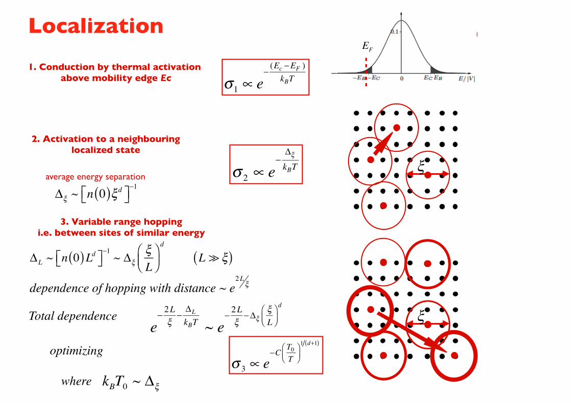
LocalizationEF
σ1 ∝ e−(Ec −EF )kBT
1. Conduction by thermal activation above mobility edge Ec
2. Activation to a neighbouringlocalized state
ξ
Δξ ~ n 0( )ξd⎡⎣ ⎤⎦−1
average energy separation σ 2 ∝ e−
Δξ
kBT
3. Variable range hoppingi.e. between sites of similar energy
ξ
ΔL ~ n 0( )Ld⎡⎣ ⎤⎦
−1~ Δξ
ξL
⎛⎝⎜
⎞⎠⎟d
L ξ( )
dependence of hopping with distance ~ e2L
ξ
Total dependencee−2Lξ
−ΔL
kBT ~ e−2Lξ
−ΔξξL
⎛⎝⎜
⎞⎠⎟d
optimizing
whereσ 3 ∝ e
−CT0T
⎛⎝⎜
⎞⎠⎟1 d+1( )
kBT0 ~ Δξ
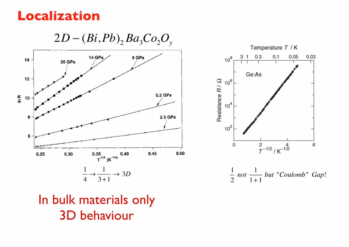
2D − (Bi,Pb)2Ba3Co2Oy
14→
13+1
→ 3D
In bulk materials only 3D behaviour
12 not 1
1+1 but "Coulomb" Gap!
Localization
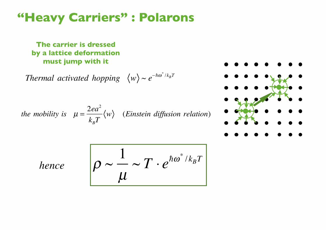
“Heavy Carriers” : Polarons
The carrier is dressedby a lattice deformation
must jump with it
Thermal activated hopping w ~ e−ω* /kBT
the mobility is µ =2ea2
kBTw (Einstein diffusion relation)
ρ ~ 1
µ~ T ⋅ eω
* /kBThence
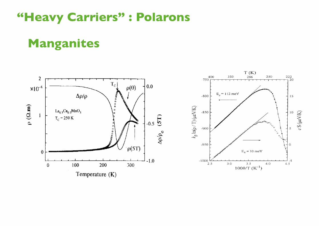
“Heavy Carriers” : Polarons
Manganites
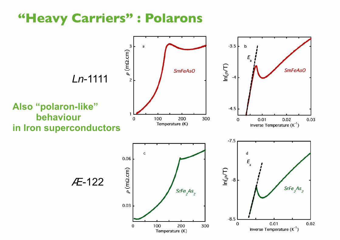
Ln-1111
Æ-122
“Heavy Carriers” : Polarons
Also “polaron-like” behaviour in Iron superconductors
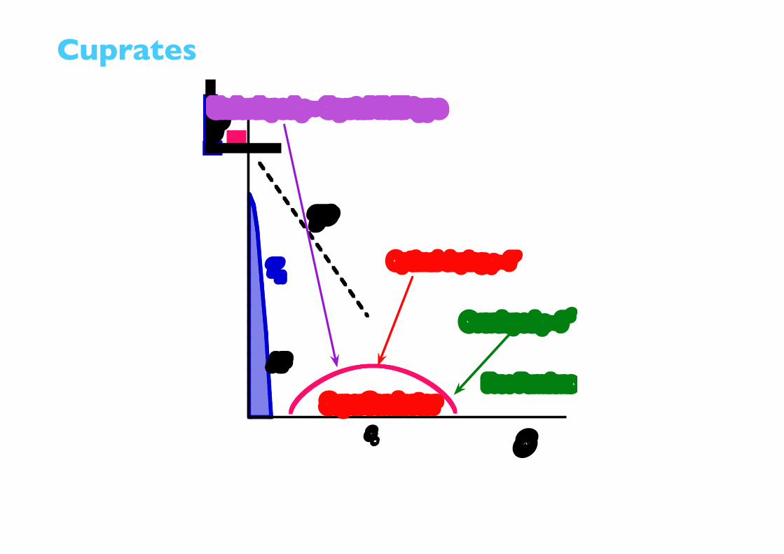
Cuprates
AF
SuperConductorFree Fermions
T*
δ
T
TN
δc
Optimal doping ρ~T
Overdoped ρ~T2
Underdoped ρ~ Crystal field type
Conclusions
The behavior of the the electrical resistivity can yield many hints into the understanding of the physics of materials


![RESISTIVITY [ ]](https://static.fdocument.org/doc/165x107/6249524a7a9f6a12787a8128/resistivity-.jpg)