
Prof. Dae Hyun Kim School of Electrical Engineering and...
52
EE582 Physical Design Automation of VLSI Circuits and Systems Prof. Dae Hyun Kim School of Electrical Engineering and Computer Science Washington State University Interconnect Optimization
Transcript of Prof. Dae Hyun Kim School of Electrical Engineering and...
EE582 Physical Design Automation of VLSI Circuits and Systems
Prof. Dae Hyun Kim
School of Electrical Engineering and Computer Science Washington State University
Interconnect Optimization
2 Physical Design Automation of VLSI Circuits and Systems
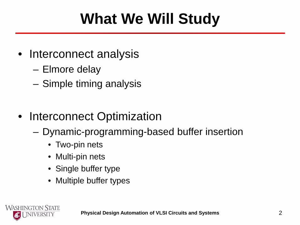
What We Will Study
• Interconnect analysis – Elmore delay – Simple timing analysis
• Interconnect Optimization
– Dynamic-programming-based buffer insertion • Two-pin nets • Multi-pin nets • Single buffer type • Multiple buffer types
3 Physical Design Automation of VLSI Circuits and Systems
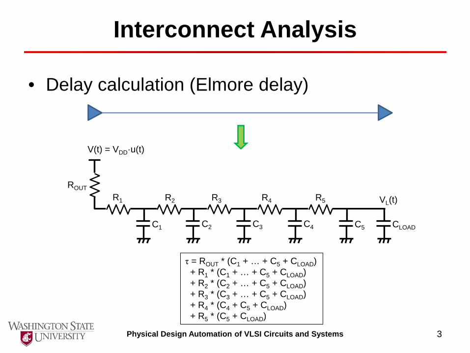
Interconnect Analysis
• Delay calculation (Elmore delay)
V(t) = VDD·u(t)
ROUT R1 R2 R3 R4 R5
C1 C2 C3 C4 C5 CLOAD
VL(t)
τ = ROUT * (C1 + … + C5 + CLOAD) + R1 * (C1 + … + C5 + CLOAD) + R2 * (C2 + … + C5 + CLOAD) + R3 * (C3 + … + C5 + CLOAD) + R4 * (C4 + C5 + CLOAD) + R5 * (C5 + CLOAD)
4 Physical Design Automation of VLSI Circuits and Systems
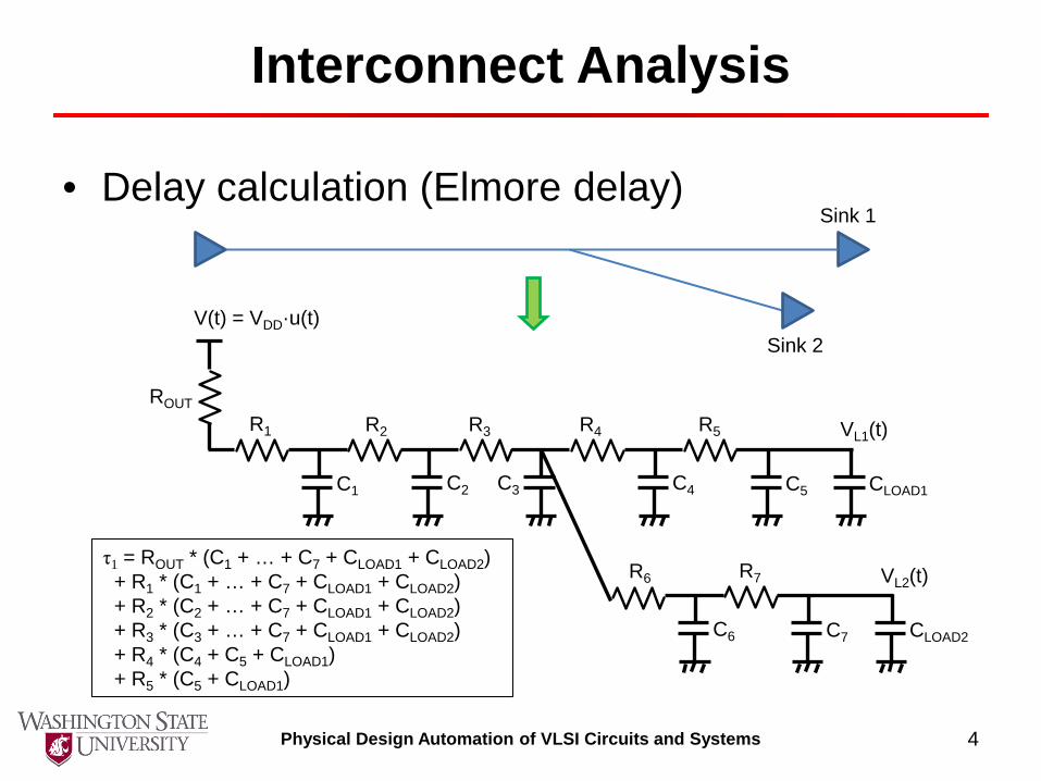
Interconnect Analysis
• Delay calculation (Elmore delay)
V(t) = VDD·u(t)
ROUT R1 R2 R3 R4 R5
C1 C2 C3 C4 C5 CLOAD1
VL1(t)
τ1 = ROUT * (C1 + … + C7 + CLOAD1 + CLOAD2) + R1 * (C1 + … + C7 + CLOAD1 + CLOAD2) + R2 * (C2 + … + C7 + CLOAD1 + CLOAD2) + R3 * (C3 + … + C7 + CLOAD1 + CLOAD2) + R4 * (C4 + C5 + CLOAD1) + R5 * (C5 + CLOAD1)
Sink 1
Sink 2
R7
C6 C7 CLOAD2
VL2(t) R6
5 Physical Design Automation of VLSI Circuits and Systems
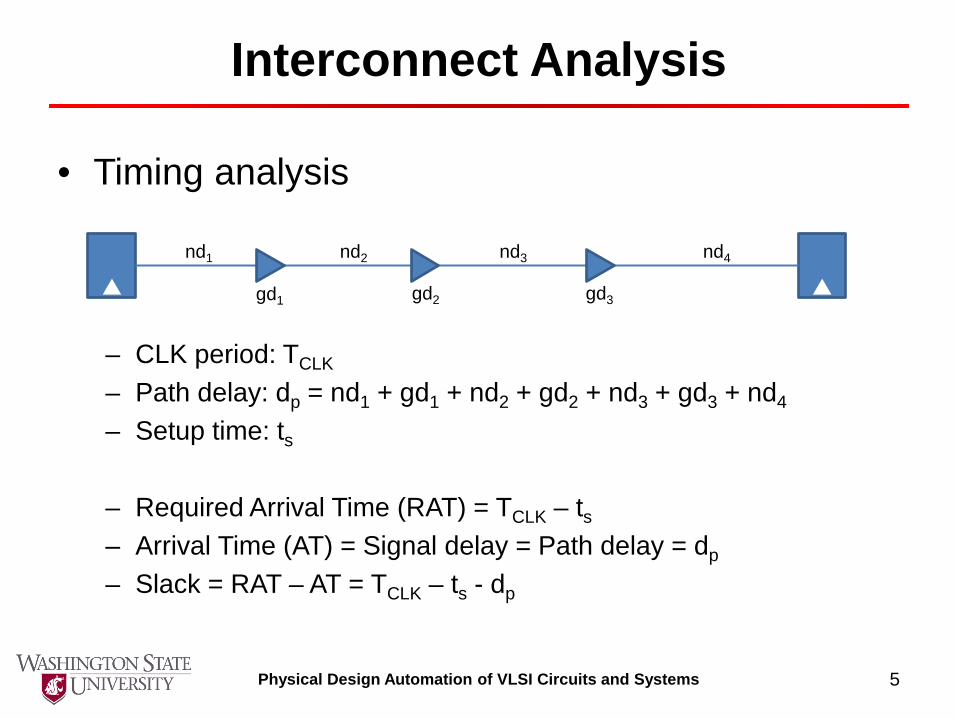
Interconnect Analysis
• Timing analysis
– CLK period: TCLK
– Path delay: dp = nd1 + gd1 + nd2 + gd2 + nd3 + gd3 + nd4 – Setup time: ts
– Required Arrival Time (RAT) = TCLK – ts
– Arrival Time (AT) = Signal delay = Path delay = dp
– Slack = RAT – AT = TCLK – ts - dp
nd1 nd2 nd3 nd4
gd1 gd2 gd3
6 Physical Design Automation of VLSI Circuits and Systems
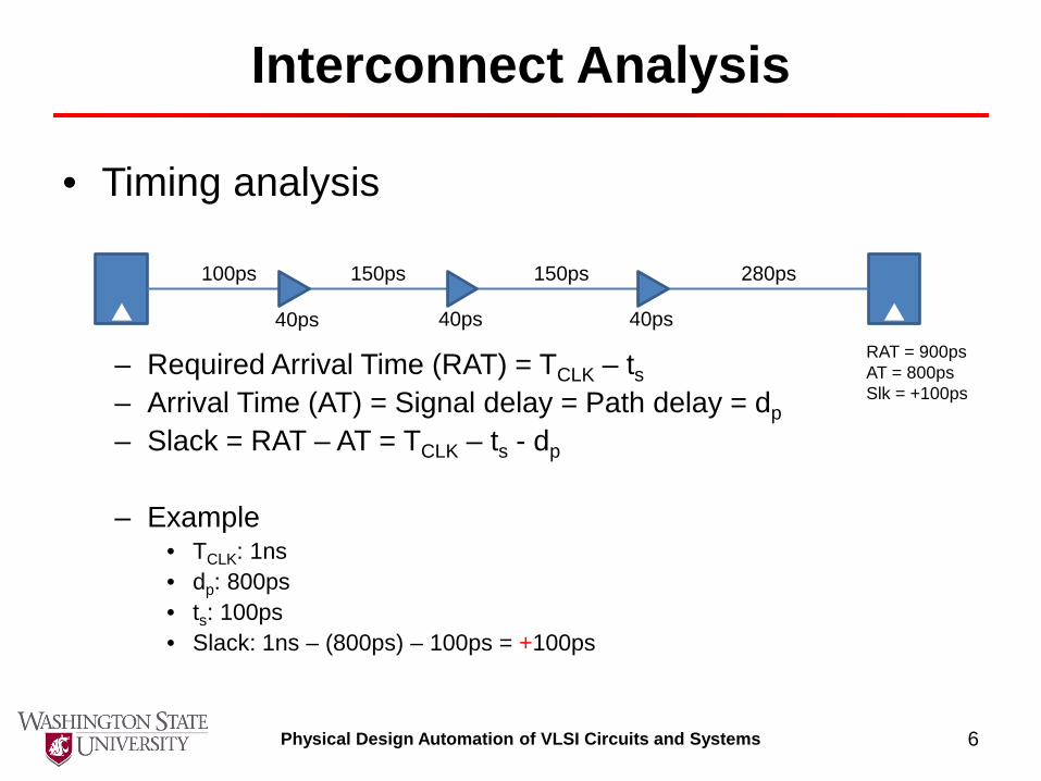
Interconnect Analysis
• Timing analysis
– Required Arrival Time (RAT) = TCLK – ts – Arrival Time (AT) = Signal delay = Path delay = dp – Slack = RAT – AT = TCLK – ts - dp
– Example
• TCLK: 1ns • dp: 800ps • ts: 100ps • Slack: 1ns – (800ps) – 100ps = +100ps
100ps 150ps 150ps 280ps
40ps 40ps 40ps
RAT = 900ps AT = 800ps Slk = +100ps
7 Physical Design Automation of VLSI Circuits and Systems
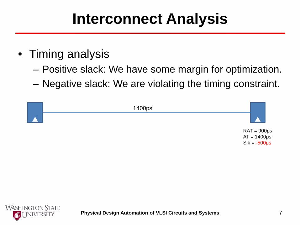
Interconnect Analysis
• Timing analysis – Positive slack: We have some margin for optimization. – Negative slack: We are violating the timing constraint.
1400ps
RAT = 900ps AT = 1400ps Slk = -500ps
8 Physical Design Automation of VLSI Circuits and Systems
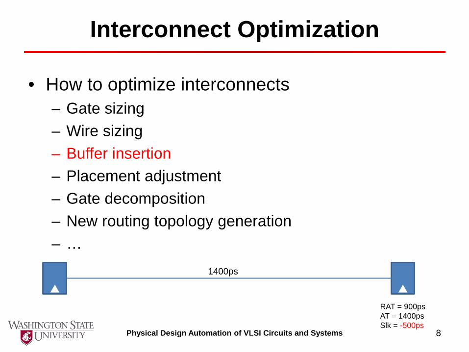
Interconnect Optimization
• How to optimize interconnects – Gate sizing – Wire sizing – Buffer insertion – Placement adjustment – Gate decomposition – New routing topology generation – …
1400ps
RAT = 900ps AT = 1400ps Slk = -500ps
9 Physical Design Automation of VLSI Circuits and Systems
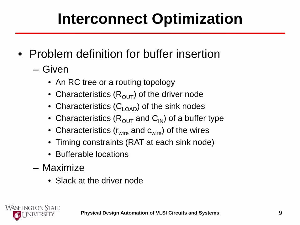
Interconnect Optimization
• Problem definition for buffer insertion – Given
• An RC tree or a routing topology • Characteristics (ROUT) of the driver node • Characteristics (CLOAD) of the sink nodes • Characteristics (ROUT and CIN) of a buffer type • Characteristics (rwire and cwire) of the wires • Timing constraints (RAT at each sink node) • Bufferable locations
– Maximize • Slack at the driver node
10 Physical Design Automation of VLSI Circuits and Systems
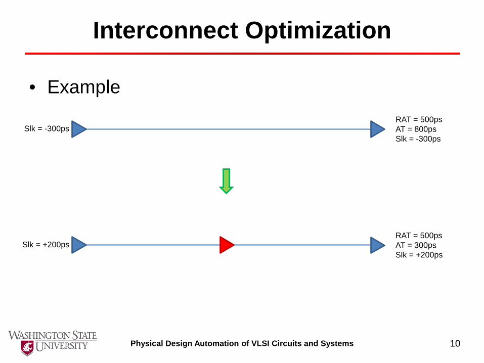
Interconnect Optimization
• Example RAT = 500ps AT = 800ps Slk = -300ps
Slk = -300ps
RAT = 500ps AT = 300ps Slk = +200ps
Slk = +200ps
11 Physical Design Automation of VLSI Circuits and Systems
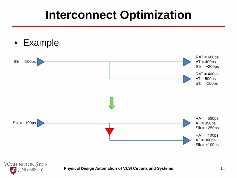
Interconnect Optimization
• Example RAT = 600ps AT = 400ps Slk = +200ps
Slk = -100ps
RAT = 400ps AT = 500ps Slk = -100ps
RAT = 600ps AT = 350ps Slk = +250ps
Slk = +100ps
RAT = 400ps AT = 300ps Slk = +100ps
12 Physical Design Automation of VLSI Circuits and Systems
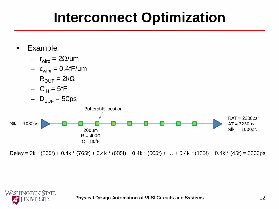
Interconnect Optimization
• Example – rwire = 2Ω/um – cwire = 0.4fF/um – ROUT = 2kΩ – CIN = 5fF – DBUF = 50ps
RAT = 2200ps AT = 3230ps Slk = -1030ps
Slk = -1030ps
Bufferable location
200um R = 400Ω C = 80fF
Delay = 2k * (805f) + 0.4k * (765f) + 0.4k * (685f) + 0.4k * (605f) + … + 0.4k * (125f) + 0.4k * (45f) = 3230ps
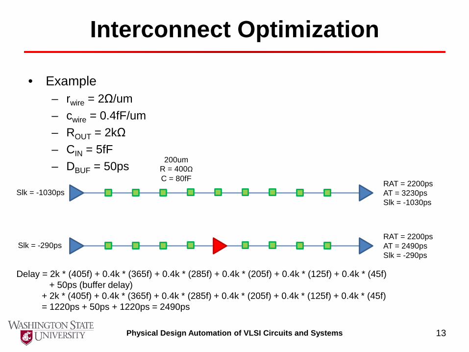
13 Physical Design Automation of VLSI Circuits and Systems
Interconnect Optimization
• Example – rwire = 2Ω/um – cwire = 0.4fF/um – ROUT = 2kΩ – CIN = 5fF – DBUF = 50ps
RAT = 2200ps AT = 3230ps Slk = -1030ps
Slk = -1030ps
200um R = 400Ω C = 80fF
RAT = 2200ps AT = 2490ps Slk = -290ps
Slk = -290ps
Delay = 2k * (405f) + 0.4k * (365f) + 0.4k * (285f) + 0.4k * (205f) + 0.4k * (125f) + 0.4k * (45f) + 50ps (buffer delay) + 2k * (405f) + 0.4k * (365f) + 0.4k * (285f) + 0.4k * (205f) + 0.4k * (125f) + 0.4k * (45f) = 1220ps + 50ps + 1220ps = 2490ps
14 Physical Design Automation of VLSI Circuits and Systems
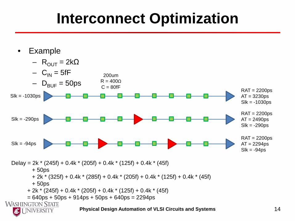
Interconnect Optimization
• Example – ROUT = 2kΩ – CIN = 5fF – DBUF = 50ps
RAT = 2200ps AT = 3230ps Slk = -1030ps
Slk = -1030ps
200um R = 400Ω C = 80fF
Delay = 2k * (245f) + 0.4k * (205f) + 0.4k * (125f) + 0.4k * (45f) + 50ps + 2k * (325f) + 0.4k * (285f) + 0.4k * (205f) + 0.4k * (125f) + 0.4k * (45f) + 50ps + 2k * (245f) + 0.4k * (205f) + 0.4k * (125f) + 0.4k * (45f) = 640ps + 50ps + 914ps + 50ps + 640ps = 2294ps
RAT = 2200ps AT = 2490ps Slk = -290ps
Slk = -290ps
RAT = 2200ps AT = 2294ps Slk = -94ps
Slk = -94ps
15 Physical Design Automation of VLSI Circuits and Systems
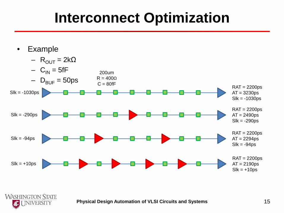
Interconnect Optimization
• Example – ROUT = 2kΩ – CIN = 5fF – DBUF = 50ps
RAT = 2200ps AT = 3230ps Slk = -1030ps
Slk = -1030ps
200um R = 400Ω C = 80fF
RAT = 2200ps AT = 2490ps Slk = -290ps
Slk = -290ps
RAT = 2200ps AT = 2294ps Slk = -94ps
Slk = -94ps
RAT = 2200ps AT = 2190ps Slk = +10ps
Slk = +10ps
16 Physical Design Automation of VLSI Circuits and Systems
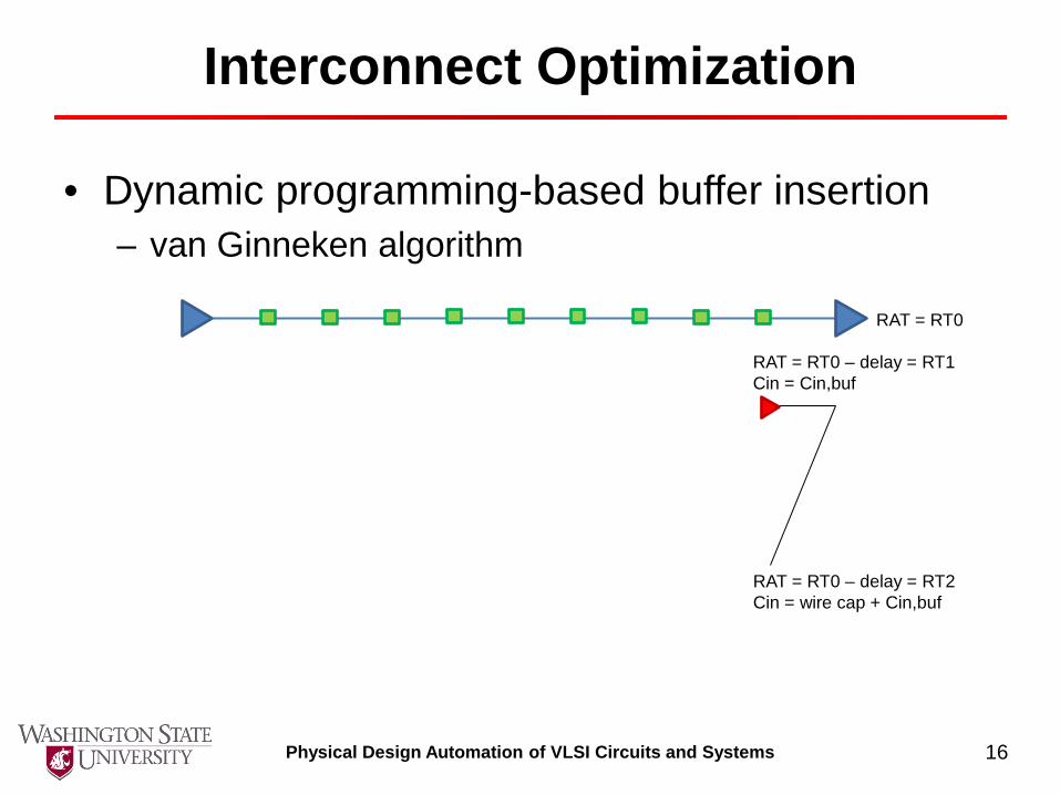
Interconnect Optimization
• Dynamic programming-based buffer insertion – van Ginneken algorithm
RAT = RT0
RAT = RT0 – delay = RT1 Cin = Cin,buf
RAT = RT0 – delay = RT2 Cin = wire cap + Cin,buf
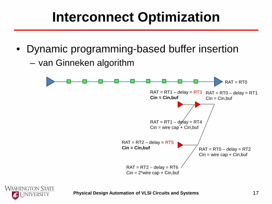
17 Physical Design Automation of VLSI Circuits and Systems
Interconnect Optimization
• Dynamic programming-based buffer insertion – van Ginneken algorithm
RAT = RT0
RAT = RT0 – delay = RT1 Cin = Cin,buf
RAT = RT0 – delay = RT2 Cin = wire cap + Cin,buf
RAT = RT1 – delay = RT3 Cin = Cin,buf
RAT = RT1 – delay = RT4 Cin = wire cap + Cin,buf
RAT = RT2 – delay = RT5 Cin = Cin,buf
RAT = RT2 – delay = RT6 Cin = 2*wire cap + Cin,buf
18 Physical Design Automation of VLSI Circuits and Systems
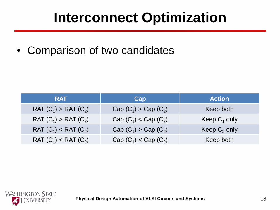
Interconnect Optimization
• Comparison of two candidates
RAT Cap Action RAT (C1) > RAT (C2) Cap (C1) > Cap (C2) Keep both RAT (C1) > RAT (C2) Cap (C1) < Cap (C2) Keep C1 only RAT (C1) < RAT (C2) Cap (C1) > Cap (C2) Keep C2 only RAT (C1) < RAT (C2) Cap (C1) < Cap (C2) Keep both
19 Physical Design Automation of VLSI Circuits and Systems
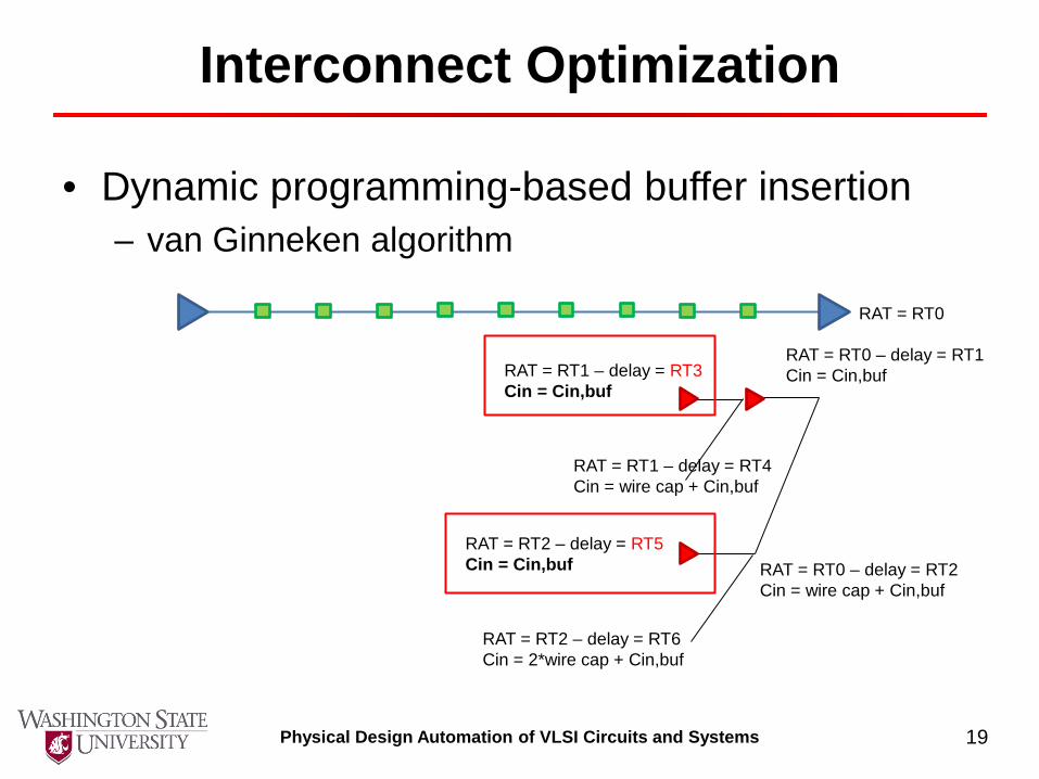
Interconnect Optimization
• Dynamic programming-based buffer insertion – van Ginneken algorithm
RAT = RT0
RAT = RT0 – delay = RT1 Cin = Cin,buf
RAT = RT0 – delay = RT2 Cin = wire cap + Cin,buf
RAT = RT1 – delay = RT3 Cin = Cin,buf
RAT = RT1 – delay = RT4 Cin = wire cap + Cin,buf
RAT = RT2 – delay = RT5 Cin = Cin,buf
RAT = RT2 – delay = RT6 Cin = 2*wire cap + Cin,buf
20 Physical Design Automation of VLSI Circuits and Systems
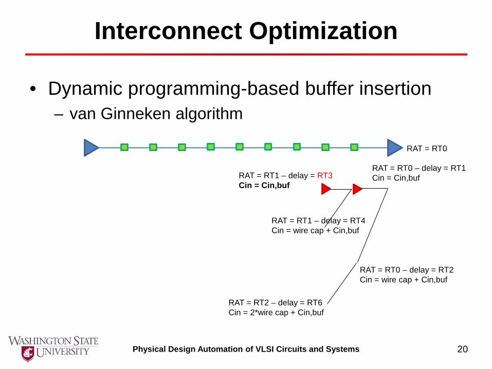
Interconnect Optimization
• Dynamic programming-based buffer insertion – van Ginneken algorithm
RAT = RT0
RAT = RT0 – delay = RT1 Cin = Cin,buf
RAT = RT0 – delay = RT2 Cin = wire cap + Cin,buf
RAT = RT1 – delay = RT3 Cin = Cin,buf
RAT = RT1 – delay = RT4 Cin = wire cap + Cin,buf
RAT = RT2 – delay = RT6 Cin = 2*wire cap + Cin,buf
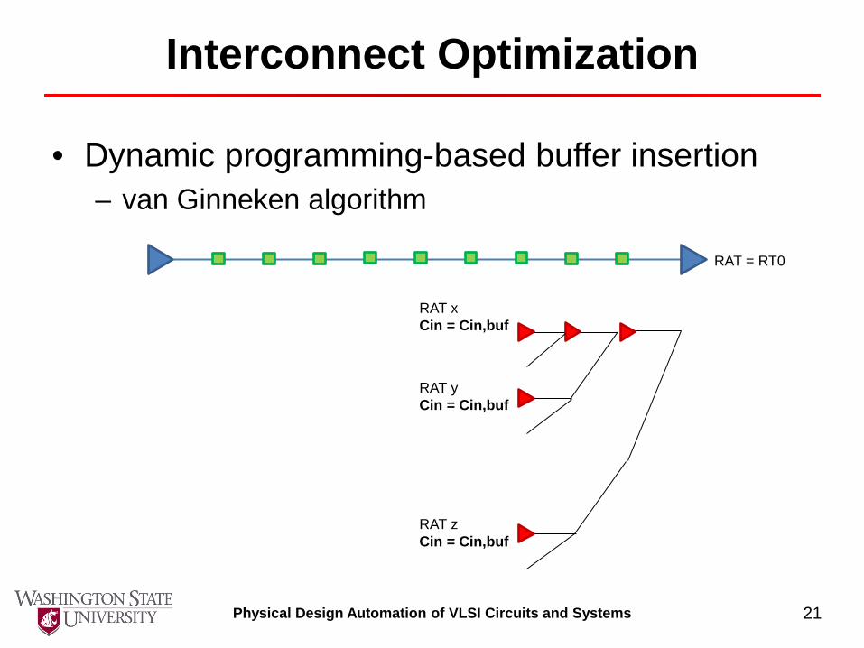
21 Physical Design Automation of VLSI Circuits and Systems
Interconnect Optimization
• Dynamic programming-based buffer insertion – van Ginneken algorithm
RAT = RT0
RAT x Cin = Cin,buf
RAT y Cin = Cin,buf
RAT z Cin = Cin,buf

22 Physical Design Automation of VLSI Circuits and Systems
Interconnect Optimization
• Dynamic programming-based buffer insertion – van Ginneken algorithm
RAT = RT0
RAT x Cin = Cin,buf
RAT y Cin = Cin,buf
RAT z Cin = Cin,buf
23 Physical Design Automation of VLSI Circuits and Systems
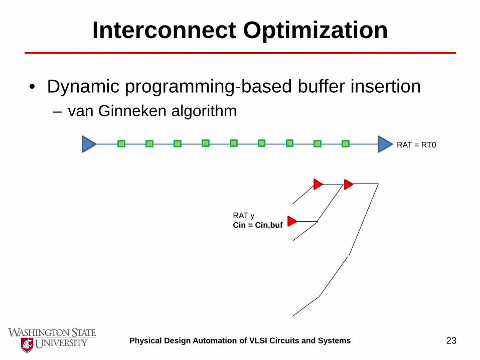
Interconnect Optimization
• Dynamic programming-based buffer insertion – van Ginneken algorithm
RAT = RT0
RAT y Cin = Cin,buf
24 Physical Design Automation of VLSI Circuits and Systems
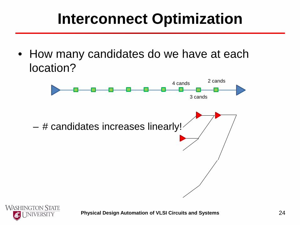
Interconnect Optimization
• How many candidates do we have at each location?
– # candidates increases linearly!
2 cands
3 cands
4 cands
25 Physical Design Automation of VLSI Circuits and Systems
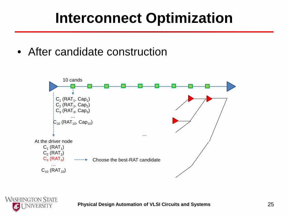
Interconnect Optimization
• After candidate construction
10 cands
C1 (RAT1, Cap1) C2 (RAT2, Cap2) C3 (RAT3, Cap3)
… C10 (RAT10, Cap10)
At the driver node C1 (RAT1) C2 (RAT2) C3 (RAT3)
… C10 (RAT10)
Choose the best-RAT candidate
…
26 Physical Design Automation of VLSI Circuits and Systems
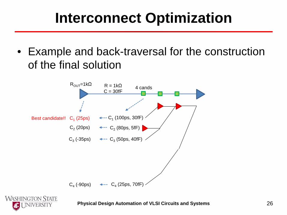
Interconnect Optimization
• Example and back-traversal for the construction of the final solution
4 cands
C1 (100ps, 30fF)
C2 (80ps, 5fF)
C3 (50ps, 40fF)
C4 (25ps, 70fF)
C1 (25ps)
R = 1kΩ C = 30fF
ROUT=1kΩ
C2 (20ps)
C3 (-35ps)
C4 (-90ps)
Best candidate!!
27 Physical Design Automation of VLSI Circuits and Systems
Interconnect Optimization
• Example
28 Physical Design Automation of VLSI Circuits and Systems
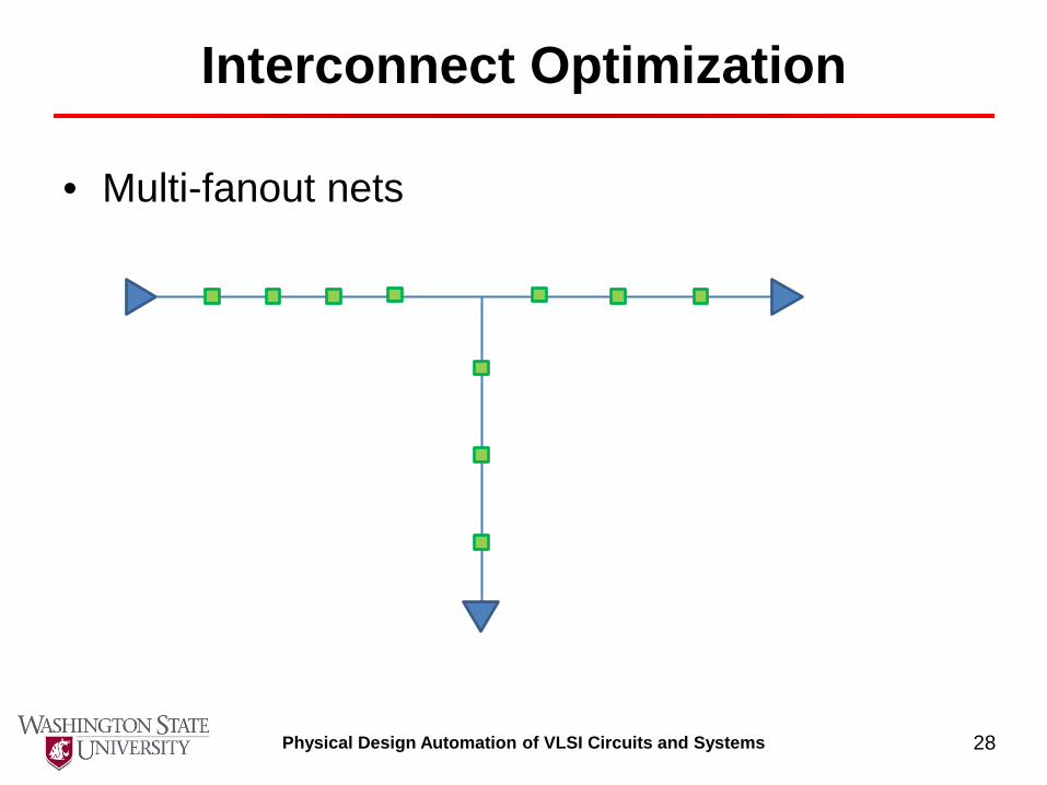
Interconnect Optimization
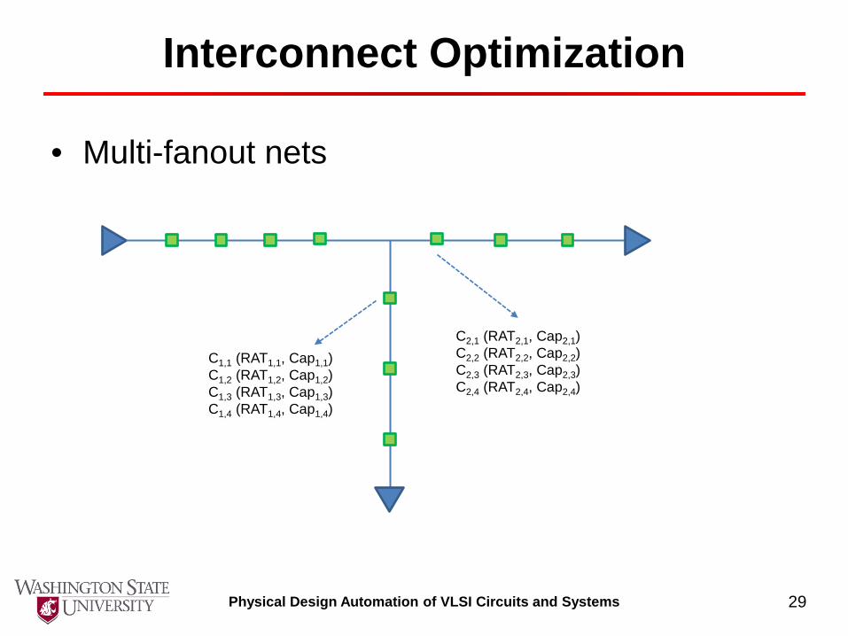
• Multi-fanout nets
29 Physical Design Automation of VLSI Circuits and Systems
Interconnect Optimization
• Multi-fanout nets
C1,1 (RAT1,1, Cap1,1) C1,2 (RAT1,2, Cap1,2) C1,3 (RAT1,3, Cap1,3) C1,4 (RAT1,4, Cap1,4)
C2,1 (RAT2,1, Cap2,1) C2,2 (RAT2,2, Cap2,2) C2,3 (RAT2,3, Cap2,3) C2,4 (RAT2,4, Cap2,4)
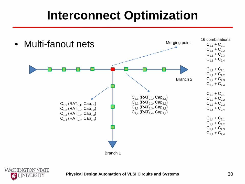
30 Physical Design Automation of VLSI Circuits and Systems
Interconnect Optimization
• Multi-fanout nets
C1,1 (RAT1,1, Cap1,1) C1,2 (RAT1,2, Cap1,2) C1,3 (RAT1,3, Cap1,3) C1,4 (RAT1,4, Cap1,4)
16 combinations C1,1 + C2,1 C1,1 + C2,2 C1,1 + C2,3 C1,1 + C2,4
C1,2 + C2,1 C1,2 + C2,2 C1,2 + C2,3 C1,2 + C2,4
C1,3 + C2,1 C1,3 + C2,2 C1,3 + C2,3 C1,3 + C2,4
C1,4 + C2,1 C1,4 + C2,2 C1,4 + C2,3 C1,4 + C2,4
Merging point
Branch 1
Branch 2
C2,1 (RAT2,1, Cap2,1) C2,2 (RAT2,2, Cap2,2) C2,3 (RAT2,3, Cap2,3) C2,4 (RAT2,4, Cap2,4)
31 Physical Design Automation of VLSI Circuits and Systems
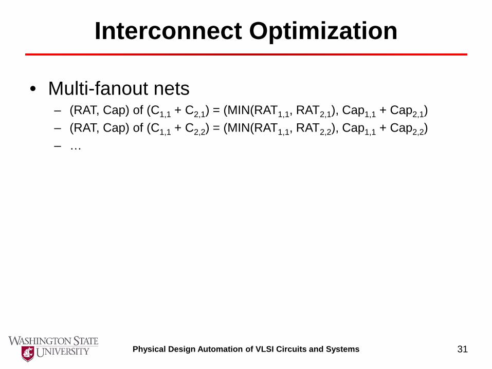
Interconnect Optimization
• Multi-fanout nets – (RAT, Cap) of (C1,1 + C2,1) = (MIN(RAT1,1, RAT2,1), Cap1,1 + Cap2,1) – (RAT, Cap) of (C1,1 + C2,2) = (MIN(RAT1,1, RAT2,2), Cap1,1 + Cap2,2) – …
32 Physical Design Automation of VLSI Circuits and Systems
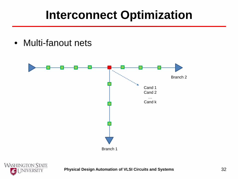
Interconnect Optimization
• Multi-fanout nets
Cand 1 Cand 2
… Cand k
Branch 1
Branch 2
33 Physical Design Automation of VLSI Circuits and Systems
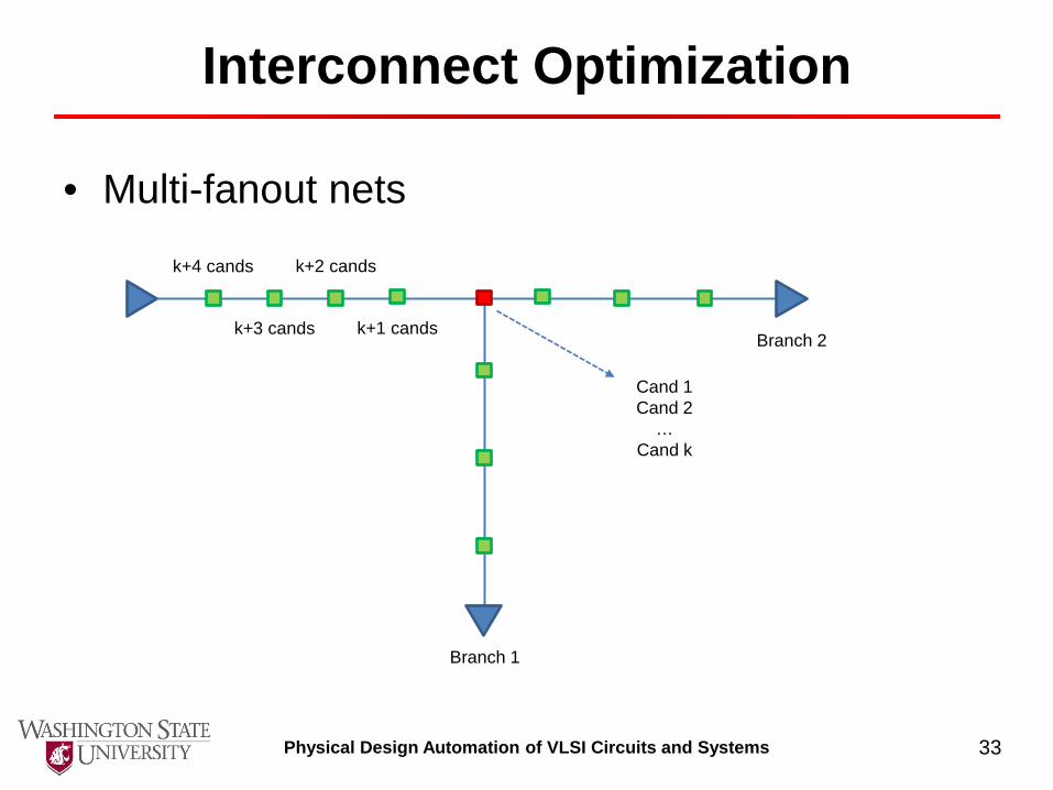
Interconnect Optimization
• Multi-fanout nets
Cand 1 Cand 2
… Cand k
Branch 1
Branch 2 k+1 cands
k+2 cands
k+3 cands
k+4 cands
34 Physical Design Automation of VLSI Circuits and Systems
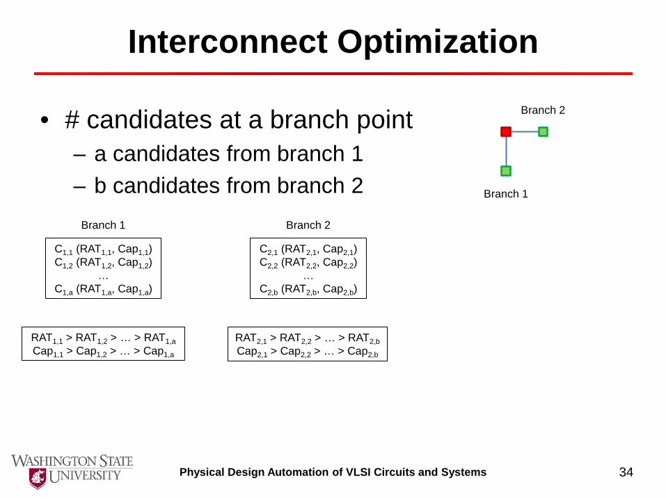
Interconnect Optimization
• # candidates at a branch point – a candidates from branch 1 – b candidates from branch 2 Branch 1
Branch 2
C1,1 (RAT1,1, Cap1,1) C1,2 (RAT1,2, Cap1,2)
… C1,a (RAT1,a, Cap1,a)
C2,1 (RAT2,1, Cap2,1) C2,2 (RAT2,2, Cap2,2)
… C2,b (RAT2,b, Cap2,b)
RAT1,1 > RAT1,2 > … > RAT1,a Cap1,1 > Cap1,2 > … > Cap1,a
RAT2,1 > RAT2,2 > … > RAT2,b Cap2,1 > Cap2,2 > … > Cap2,b
Branch 1 Branch 2
35 Physical Design Automation of VLSI Circuits and Systems
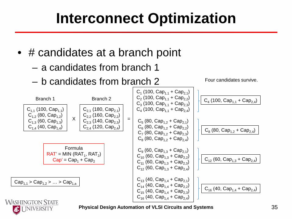
Interconnect Optimization
• # candidates at a branch point – a candidates from branch 1 – b candidates from branch 2
C1,1 (100, Cap1,1) C1,2 (80, Cap1,2) C1,3 (60, Cap1,3) C1,4 (40, Cap1,4)
C2,1 (180, Cap2,1) C2,2 (160, Cap2,2) C2,3 (140, Cap2,3) C2,4 (120, Cap2,4)
Branch 1 Branch 2
X
C1 (100, Cap1,1 + Cap2,1) C2 (100, Cap1,1 + Cap2,2) C3 (100, Cap1,1 + Cap2,3) C4 (100, Cap1,1 + Cap2,4)
C5 (80, Cap1,2 + Cap2,1) C6 (80, Cap1,2 + Cap2,2) C7 (80, Cap1,2 + Cap2,3) C8 (80, Cap1,2 + Cap2,4)
C9 (60, Cap1,3 + Cap2,1) C10 (60, Cap1,3 + Cap2,2) C11 (60, Cap1,3 + Cap2,3) C12 (60, Cap1,3 + Cap2,4)
C13 (40, Cap1,4 + Cap2,1) C14 (40, Cap1,4 + Cap2,2) C15 (40, Cap1,4 + Cap2,3) C16 (40, Cap1,4 + Cap2,4)
=
Formula RAT’ = MIN (RAT1, RAT2)
Cap’ = Cap1 + Cap2
Cap1,1 > Cap1,2 > … > Cap1,a
C4 (100, Cap1,1 + Cap2,4)
C8 (80, Cap1,2 + Cap2,4)
C12 (60, Cap1,3 + Cap2,4)
C16 (40, Cap1,4 + Cap2,4)
Four candidates survive.
36 Physical Design Automation of VLSI Circuits and Systems
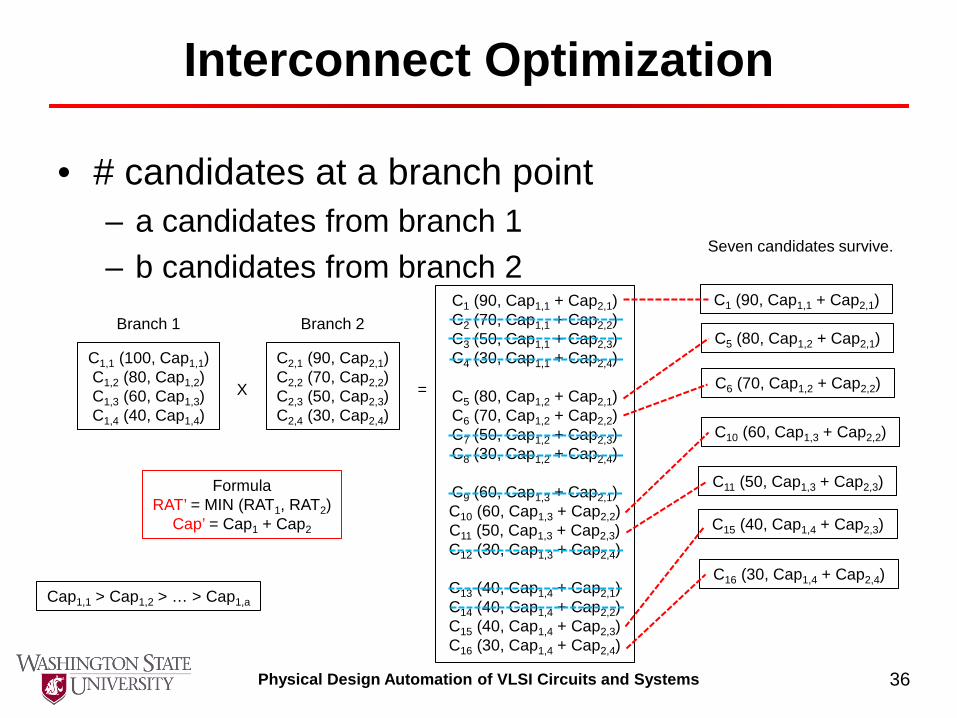
Interconnect Optimization
• # candidates at a branch point – a candidates from branch 1 – b candidates from branch 2
C1,1 (100, Cap1,1) C1,2 (80, Cap1,2) C1,3 (60, Cap1,3) C1,4 (40, Cap1,4)
C2,1 (90, Cap2,1) C2,2 (70, Cap2,2) C2,3 (50, Cap2,3) C2,4 (30, Cap2,4)
Branch 1 Branch 2
X
C1 (90, Cap1,1 + Cap2,1) C2 (70, Cap1,1 + Cap2,2) C3 (50, Cap1,1 + Cap2,3) C4 (30, Cap1,1 + Cap2,4)
C5 (80, Cap1,2 + Cap2,1) C6 (70, Cap1,2 + Cap2,2) C7 (50, Cap1,2 + Cap2,3) C8 (30, Cap1,2 + Cap2,4)
C9 (60, Cap1,3 + Cap2,1) C10 (60, Cap1,3 + Cap2,2) C11 (50, Cap1,3 + Cap2,3) C12 (30, Cap1,3 + Cap2,4)
C13 (40, Cap1,4 + Cap2,1) C14 (40, Cap1,4 + Cap2,2) C15 (40, Cap1,4 + Cap2,3) C16 (30, Cap1,4 + Cap2,4)
=
Formula RAT’ = MIN (RAT1, RAT2)
Cap’ = Cap1 + Cap2
Cap1,1 > Cap1,2 > … > Cap1,a
C1 (90, Cap1,1 + Cap2,1)
C6 (70, Cap1,2 + Cap2,2)
C11 (50, Cap1,3 + Cap2,3)
C15 (40, Cap1,4 + Cap2,3)
C5 (80, Cap1,2 + Cap2,1)
C10 (60, Cap1,3 + Cap2,2)
C16 (30, Cap1,4 + Cap2,4)
Seven candidates survive.
37 Physical Design Automation of VLSI Circuits and Systems
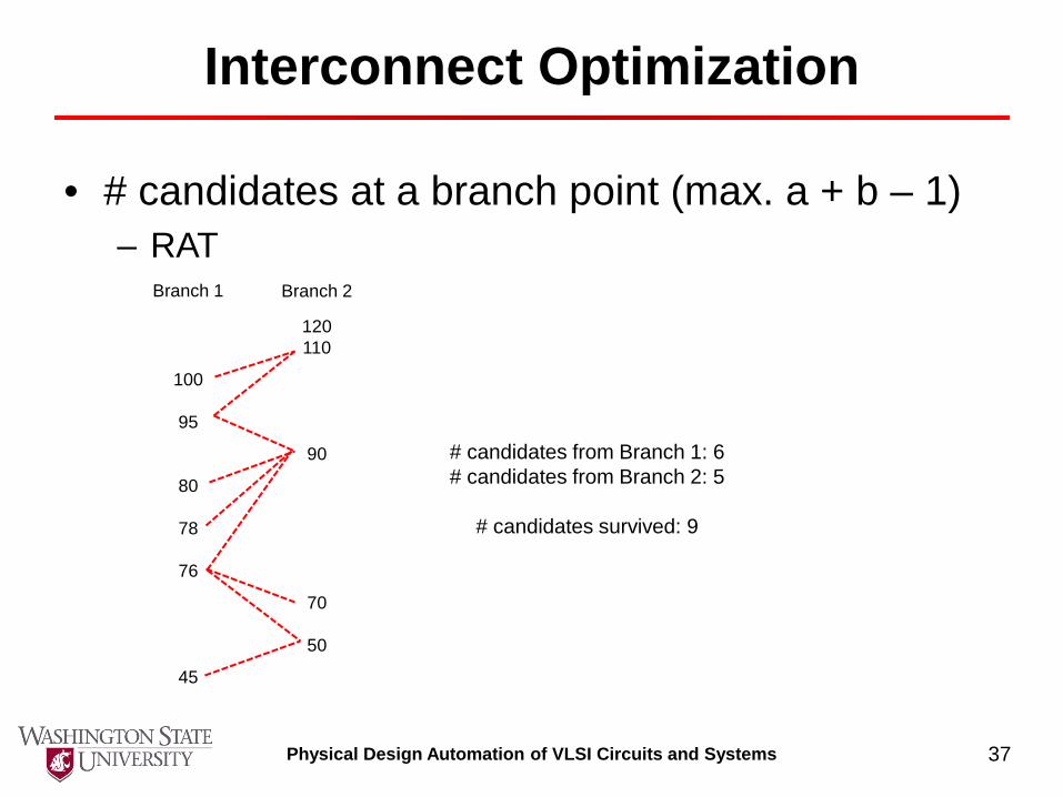
Interconnect Optimization
• # candidates at a branch point (max. a + b – 1) – RAT
Branch 1
100
95
80
78
76
45
Branch 2
120 110
90
70
50
# candidates from Branch 1: 6 # candidates from Branch 2: 5
# candidates survived: 9
38 Physical Design Automation of VLSI Circuits and Systems
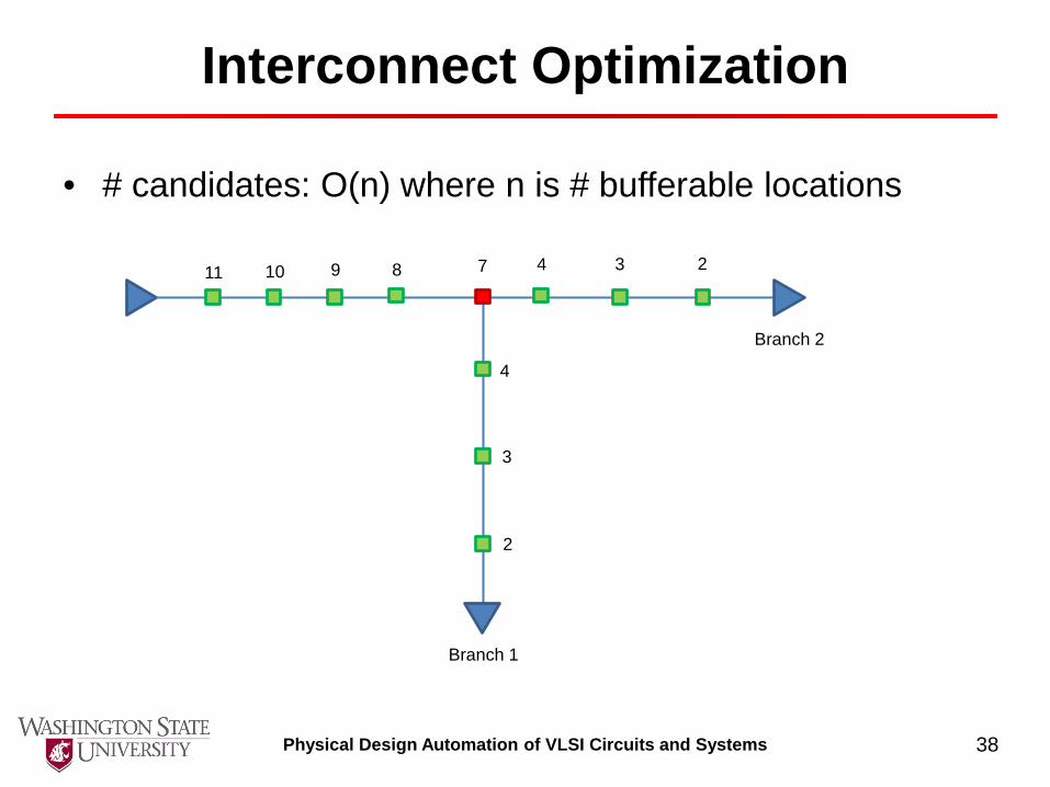
Interconnect Optimization
• # candidates: O(n) where n is # bufferable locations
Branch 1
Branch 2
2
3
4
4 3 2 7 8 9 10 11
39 Physical Design Automation of VLSI Circuits and Systems
Interconnect Optimization
• This page is left blank intentionally.
40 Physical Design Automation of VLSI Circuits and Systems
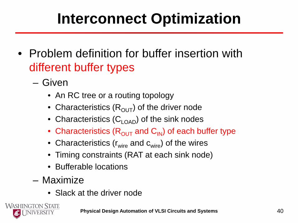
Interconnect Optimization
• Problem definition for buffer insertion with different buffer types – Given
• An RC tree or a routing topology • Characteristics (ROUT) of the driver node • Characteristics (CLOAD) of the sink nodes • Characteristics (ROUT and CIN) of each buffer type • Characteristics (rwire and cwire) of the wires • Timing constraints (RAT at each sink node) • Bufferable locations
– Maximize • Slack at the driver node
41 Physical Design Automation of VLSI Circuits and Systems
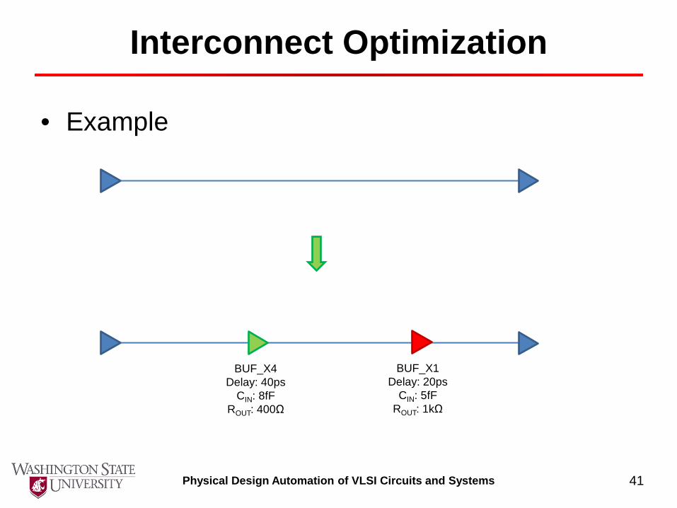
Interconnect Optimization
• Example
BUF_X1 Delay: 20ps
CIN: 5fF ROUT: 1kΩ
BUF_X4 Delay: 40ps
CIN: 8fF ROUT: 400Ω
42 Physical Design Automation of VLSI Circuits and Systems
Interconnect Optimization
• Handling multiple buffer types can be done in the same way.
• The complexity goes up.
43 Physical Design Automation of VLSI Circuits and Systems
Interconnect Optimization
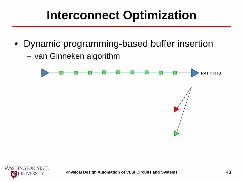
• Dynamic programming-based buffer insertion – van Ginneken algorithm
RAT = RT0
44 Physical Design Automation of VLSI Circuits and Systems
Interconnect Optimization
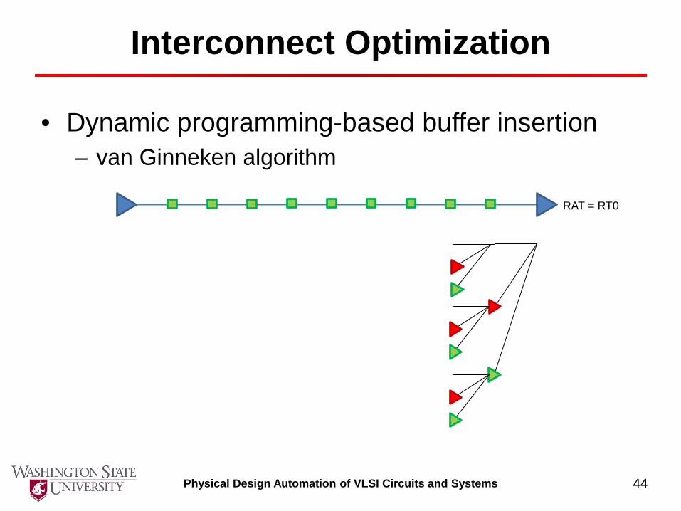
• Dynamic programming-based buffer insertion – van Ginneken algorithm
RAT = RT0
45 Physical Design Automation of VLSI Circuits and Systems
Interconnect Optimization
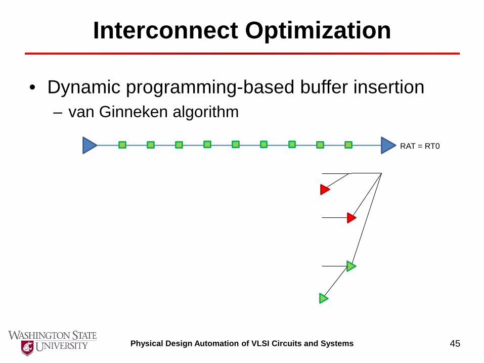
• Dynamic programming-based buffer insertion – van Ginneken algorithm
RAT = RT0
46 Physical Design Automation of VLSI Circuits and Systems
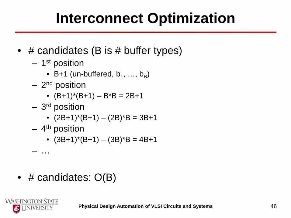
Interconnect Optimization
• # candidates (B is # buffer types) – 1st position
• B+1 (un-buffered, b1, …, bB) – 2nd position
• (B+1)*(B+1) – B*B = 2B+1 – 3rd position
• (2B+1)*(B+1) – (2B)*B = 3B+1 – 4th position
• (3B+1)*(B+1) – (3B)*B = 4B+1 – …
• # candidates: O(B)

47 Physical Design Automation of VLSI Circuits and Systems
Interconnect Optimization
• This page is left blank intentionally.

48 Physical Design Automation of VLSI Circuits and Systems
Interconnect Optimization
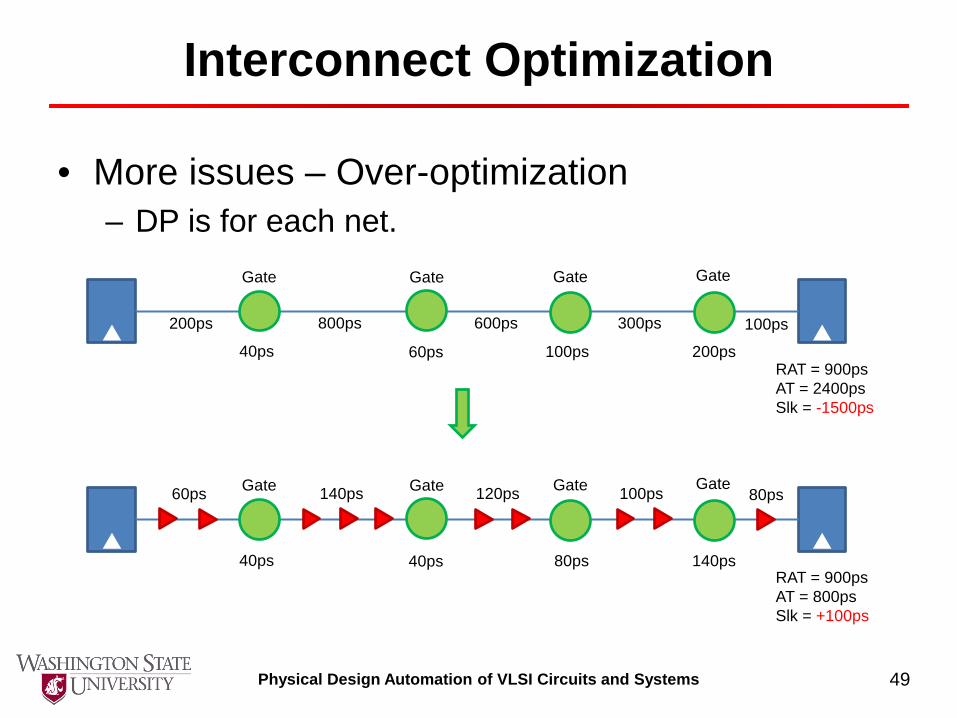
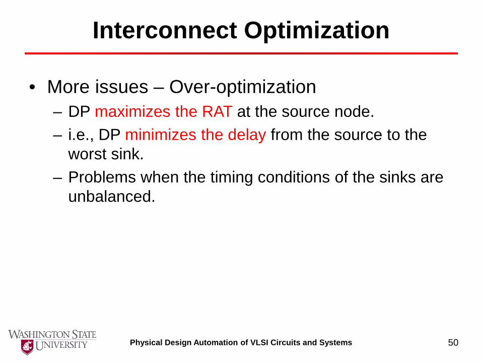
• More issues – Over-optimization – DP is for each net.
RAT = 900ps AT = 2400ps Slk = -1500ps
Gate Gate Gate Gate
RAT = 900ps AT = 800ps Slk = +100ps
Gate Gate Gate Gate
40ps 60ps 100ps 200ps
200ps 800ps 600ps 300ps 100ps
40ps 40ps 80ps 140ps
60ps 140ps 120ps 100ps 80ps
49 Physical Design Automation of VLSI Circuits and Systems
Interconnect Optimization
• More issues – Over-optimization – DP is for each net.
RAT = 900ps AT = 2400ps Slk = -1500ps
Gate Gate Gate Gate
RAT = 900ps AT = 800ps Slk = +100ps
Gate Gate Gate Gate
40ps 60ps 100ps 200ps
200ps 800ps 600ps 300ps 100ps
40ps 40ps 80ps 140ps
60ps 140ps 120ps 100ps 80ps
50 Physical Design Automation of VLSI Circuits and Systems
Interconnect Optimization
• More issues – Over-optimization – DP maximizes the RAT at the source node. – i.e., DP minimizes the delay from the source to the
worst sink. – Problems when the timing conditions of the sinks are
unbalanced.
51 Physical Design Automation of VLSI Circuits and Systems
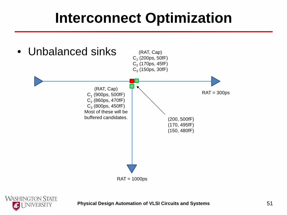
Interconnect Optimization
• Unbalanced sinks
RAT = 1000ps
RAT = 300ps
(RAT, Cap) C1 (200ps, 50fF) C2 (170ps, 45fF) C3 (150ps, 30fF)
(RAT, Cap) C1 (900ps, 500fF) C2 (860ps, 470fF) C3 (800ps, 450fF)
Most of these will be buffered candidates. (200, 500fF)
(170, 495fF) (150, 480fF)
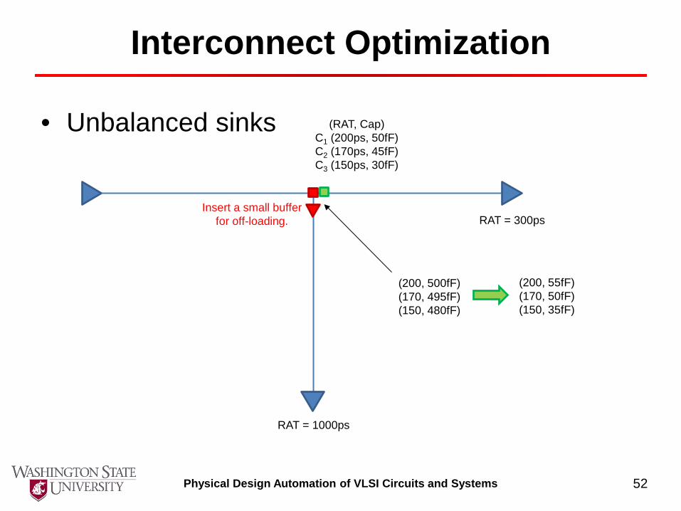
52 Physical Design Automation of VLSI Circuits and Systems
Interconnect Optimization
• Unbalanced sinks
RAT = 1000ps
RAT = 300ps
(RAT, Cap) C1 (200ps, 50fF) C2 (170ps, 45fF) C3 (150ps, 30fF)
(200, 500fF) (170, 495fF) (150, 480fF)
Insert a small buffer for off-loading.
(200, 55fF) (170, 50fF) (150, 35fF)


![Section 10-VLSI.ppt [Λειτουργία συμβατότητας]tsiatouhas/MYE018-VLSI/Section_10-2p.pdf– Χρήση διατάξεων λογικής (logic arrays) – Χρήση](https://static.fdocument.org/doc/165x107/5f40734e54435a1a9225c716/section-10-vlsippt-foe-tsiatouhasmye018-vlsisection10-2ppdf.jpg)