Proceedings - Rochester Institute of Technologyedge.rit.edu/.../P13071TechnicalPaper-12.docx · Web...
14
Multidisciplinary Senior Design Conference Kate Gleason College of Engineering Rochester Institute of Technology Rochester, New York 14623 Project Number: P13071 NON-INVASIVE BLOOD GLUCOSE MONITOR Jared Bold EE Yongjie Cao EE John Louma EE Andrew Rosen EE Daniel Sinkiewicz EE Abstract Blood glucose monitoring is a valuable tool not only for diabetic individuals working to maintain a healthy lifestyle, but also for physicians charged with caring for patients. Today's most accurate blood glucose monitoring systems are invasive in nature, requiring direct access to a patient's blood for optimal analysis. As an alternative to these invasive techniques, the Non-Invasive Blood Glucose Monitor has been developed. Most measurement systems are invasive because they rely on sensors that chemically interact with the glucose in blood. The non-invasive monitor takes a different approach and instead works based on how glucose changes the dielectric properties of blood. This device utilizes an RF synthesizer and a vector measurement system to sweep through a specified band of frequencies and monitor shifts in an antenna’s resonant frequency. The vector measurement obtained can be correlated to a patient’s blood glucose level. This data is transferred from the device to a PC where it is processed and is displayed in real-time. In addition, the transmission through the forearm is measured using the secondary antenna and captured for use in future research. Nomenclature Our device measures two parameters: the reflection S 11 and the transmission S 21 . Copyright © 2013 Rochester Institute of Technology
Transcript of Proceedings - Rochester Institute of Technologyedge.rit.edu/.../P13071TechnicalPaper-12.docx · Web...
Multidisciplinary Senior Design ConferenceKate Gleason College of Engineering
Rochester Institute of TechnologyRochester, New York 14623
Project Number: P13071
NON-INVASIVE BLOOD GLUCOSE MONITOR
Jared BoldEE
Yongjie CaoEE
John LoumaEE
Andrew RosenEE
Daniel SinkiewiczEE
Abstract Blood glucose monitoring is a valuable tool not only for diabetic individuals working to maintain a healthy lifestyle, but also for physicians charged with caring for patients. Today's most accurate blood glucose monitoring systems are invasive in nature, requiring direct access to a patient's blood for optimal analysis. As an alternative to these invasive techniques, the Non-Invasive Blood Glucose Monitor has been developed. Most measurement systems are invasive because they rely on sensors that chemically interact with the glucose in blood. The non-invasive monitor takes a different approach and instead works based on how glucose changes the dielectric properties of blood. This device utilizes an RF synthesizer and a vector measurement system to sweep through a specified band of frequencies and monitor shifts in an antenna’s resonant frequency. The vector measurement obtained can be correlated to a patient’s blood glucose level. This data is transferred from the device to a PC where it is processed and is displayed in real-time. In addition, the transmission through the forearm is measured using the secondary antenna and captured for use in future research.
NomenclatureOur device measures two parameters: the reflection S11 and the transmission S21.
S11=a1
b1 S21=
b2
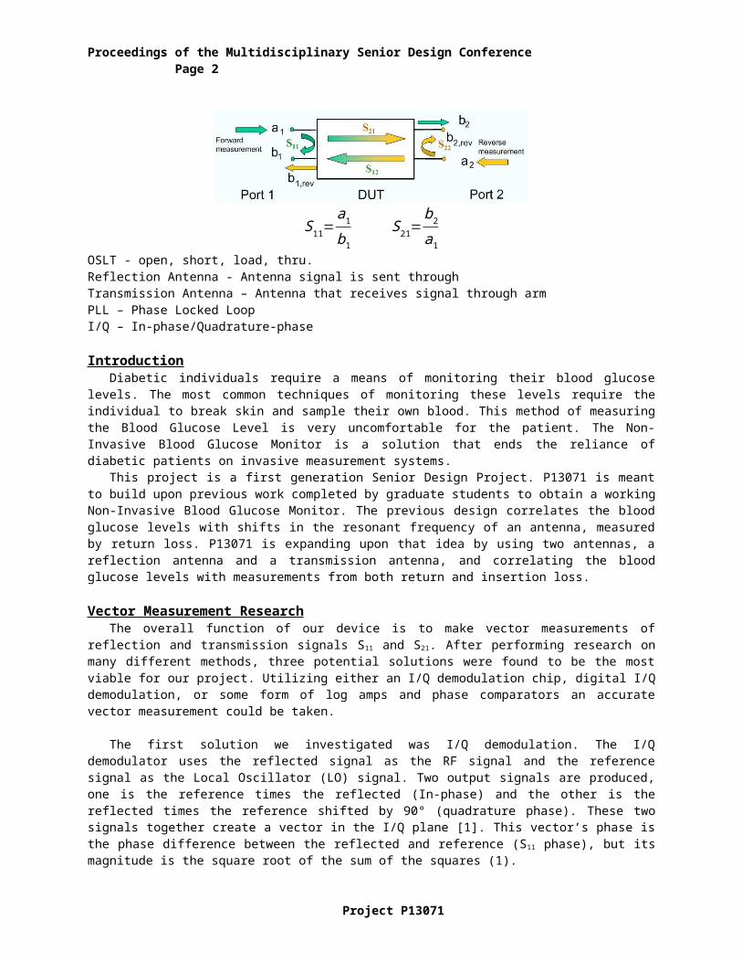
a1OSLT - open, short, load, thru.Reflection Antenna - Antenna signal is sent throughTransmission Antenna – Antenna that receives signal through armPLL – Phase Locked LoopI/Q – In-phase/Quadrature-phase
Introduction
Copyright © 2013 Rochester Institute of Technology
Proceedings of the Multidisciplinary Senior Design Conference Page 2
Diabetic individuals require a means of monitoring their blood glucose levels. The most common techniques of monitoring these levels require the individual to break skin and sample their own blood. This method of measuring the Blood Glucose Level is very uncomfortable for the patient. The Non-Invasive Blood Glucose Monitor is a solution that ends the reliance of diabetic patients on invasive measurement systems.
This project is a first generation Senior Design Project. P13071 is meant to build upon previous work completed by graduate students to obtain a working Non-Invasive Blood Glucose Monitor. The previous design correlates the blood glucose levels with shifts in the resonant frequency of an antenna, measured by return loss. P13071 is expanding upon that idea by using two antennas, a reflection antenna and a transmission antenna, and correlating the blood glucose levels with measurements from both return and insertion loss.
Vector Measurement ResearchThe overall function of our device is to make vector measurements of reflection and transmission signals S 11
and S21. After performing research on many different methods, three potential solutions were found to be the most viable for our project. Utilizing either an I/Q demodulation chip, digital I/Q demodulation, or some form of log amps and phase comparators an accurate vector measurement could be taken.
The first solution we investigated was I/Q demodulation. The I/Q demodulator uses the reflected signal as the RF signal and the reference signal as the Local Oscillator (LO) signal. Two output signals are produced, one is the reference times the reflected (In-phase) and the other is the reflected times the reference shifted by 90° (quadrature phase). These two signals together create a vector in the I/Q plane [1]. This vector’s phase is the phase difference between the reflected and reference (S11 phase), but its magnitude is the square root of the sum of the squares (1).
√|a1|2+|b1|
2 (1)
Both signals are introduced to the demodulation chip through a coupler, and their magnitudes will be attenuated by the coupler as a function of frequency. In order to determine the magnitude of S11, we will have to mathematically calculate the amplitude of the reference signal after the coupler and solve for the magnitude of the reflected signal using the magnitudes of the I/Q vector and the reference signal. Once the magnitude of the reflected signal has been determined, we can mathematically calculated the magnitude of S11. In this arrangement, we would have an accurate measurement of the S11 phase, but we will have to mathematically determine the magnitude of S11. Error could be introduced during these mathematical calculations because we will have to hard code the equation for the magnitude. If, for example, the coupler attenuated the signal less during one sampling it could result in an inaccurate S11 magnitude. Therefore, the use of an I/Q demodulation chip is not an accurate enough method of vector measurement.
Another method for vector measurements would be digital I/Q demodulation, which would digitize the reference, reflected, and transmitted signals then perform I/Q demodulation on the digital signals. This method has the benefit of reducing the amount of error introduced into the signals through the analog processing a standard I/Q demodulation chip performs. Sampling these three lines presents an enormous problem though. The three lines would have to be sampled simultaneously in order to retain the proper phase in all signals. This could be accomplished with a more powerful onboard processor, but the amount of data transferred to the computer at the same time would be large. The signals would also have to be mixed to an IF and filtered in order to assure the sampled signals will not contain extraneous content [2]. This means three separate transmission lines (four during calibration) will have to be simultaneously mixed down, filtered, and then sampled. Another synthesizer would be required to mix down the signals, and the development of the transmission lines would have to be carefully controlled in order to keep the signals in phase. Digital I/Q demodulation introduces many potential sources of error, and is unlikely to produce a working vector measurement.
The AD8302 chip contains a phase comparator and logarithmic amplifier which are used to determine the phase and magnitude difference between two input signals. It measures phase difference by simply utilizing the phase comparator on the two input signals. A magnitude measurement is accomplished by using log amp division between the two input signals. This chip has already been proven to be a feasible solution because it was used in Ben Freer’s circuitry for his original thesis project [5]. After consulting with the application engineers at Analog Devices we settled on using the AD8302 to obtain vector measurements. The chip is specifically designed to compare two signals, while I/Q demodulation is not. In normal I/Q demodulation implementation, the carrier (LO) signal is a
Project P13071
Proceedings of the Multi-Disciplinary Senior Design Conference Page 3
sinusoidal function with unit amplitude. In this implementation the carrier signal will have its own magnitude, which is why additional processing is required to obtain the desired values. Also, I/Q demodulation is designed to break a signal out into a Cartesian coordinate system but in this implementation we would convert the Cartesian results back into polar notation, which eliminates the primary functionality of this technique. The AD8302 is designed around recording a vector measurement between two signals in an easily implementable fashion, so it was chosen as our solution.
Micro Control Unit The choice of microcontroller came down to a few factors. First, the clock rate needed to be at least 25 MHz in
order to sample and transmit the data in the time range desired, and the chosen PLL required a 25MHz reference signal. Next, the ADCs were desired to have at least 12 bit resolution. The final criterion was the familiarity with the microcontroller. Multiple team members had ample experience programming MSP430s.
RF Synthesizer (PLL)A PLL)was selected as our RF synthesizer because it is a powerful control circuit that can maintain an accurate
frequency signal. This feature is required for our design because the device requires a steady signal in order to make high resolution frequency measurements. If the signal frequency varies during the measurement, there will be some error associated with the determined resonant frequency. The main criterion for the PLL was for it to have an operational frequency range including 800 – 2000 MHz, which is our frequency sweep range. The second criterion was an internal Voltage Controller Oscillator (VCO), which is preferable to an external VCO circuit. An internal VCO means that there is less circuitry implemented by our group, therefore less room for error. The ADF4351 was selected over other PLLs because Analog Devices has produced multiple supporting documents and software packages for their products, along with applications engineers on call.
Power AmplifierThere were two main reasons for choosing the power amplifier on our device. First, it is well matched across
our frequency band of operation (800-2000 MHz). Second, we want to amplify the power output from the antenna to the maximum power level possible (cell phone level ~23dBm) in order to receive transmission through the arm.
Harmonic FiltersOur system uses several non-linear devices, and when any non-linear device is used for analog circuitry
harmonics will be generated. Harmonics are signals at multiples of the frequency of operation. For example, in our system if we use an 800 MHz signal there will be harmonics generated at1600 , 2400 ,… ,n∗800 where nϵ N . To get rid of the harmonics in our system we used two low pass filters that divided our band of operation. One filter was set to 1200MHz, through which signals under 1200MHz were passed. Once the sweep signal reached 1200MHz the path was switched and the signal was routed through a 2400MHz low pass filter. This process ensures no harmonic frequencies will be introduced into our frequency band of interest.
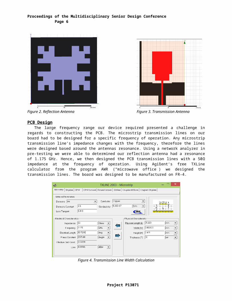
Antenna DesignFor our device the maximum frequency of operation has to be 2GHz or lower to allow for appropriate
penetration of the RF signal. Every patient’s body is different, which could result in a wide variety of shifting the natural resonant frequency of the antenna. Also, since the frequency range of our device was chosen to be 800-2000 MHz, a frequency of 1100 MHz would be appropriate for the reflection antenna. In addition, the reflection antenna needs to be of narrowband nature to have a sharp resonant frequency for detection. With these desired characteristics a simple microstrip patch antenna would suit our needs, but at this frequency the size of the antenna would be relatively large compared to the arm. Finding a purchasable antenna is too difficult due to the desired antenna’s resonant frequency, which is an uncommon frequency used in commercial products, and the required size of the antenna. With the too high of a risk in purchasing an antenna it would be more ideal to design and manufacture an antenna despite the potentially higher cost of manufacturing.
The reflection antenna design, is a modified microstrip patch using size reduction techniques. The technique used to modify the patch involved creating rectangular cutouts. In a regular microstrip patch the current flows around the outside of the structure. By creating these rectangular cutouts the current now flows around in an electrically larger antenna, which lowers the resonant frequency. The transmission antenna needs to be wideband, across our frequency range, in order to detect any possible signal that could travel through the arm. This antenna was taken from a wideband co-planar antenna [4] and modified slightly to work in our frequency range.
Copyright © 2008 Rochester Institute of Technology
Proceedings of the Multidisciplinary Senior Design Conference Page 4
Figure 2. Reflection Antenna Figure 3. Transmission Antenna
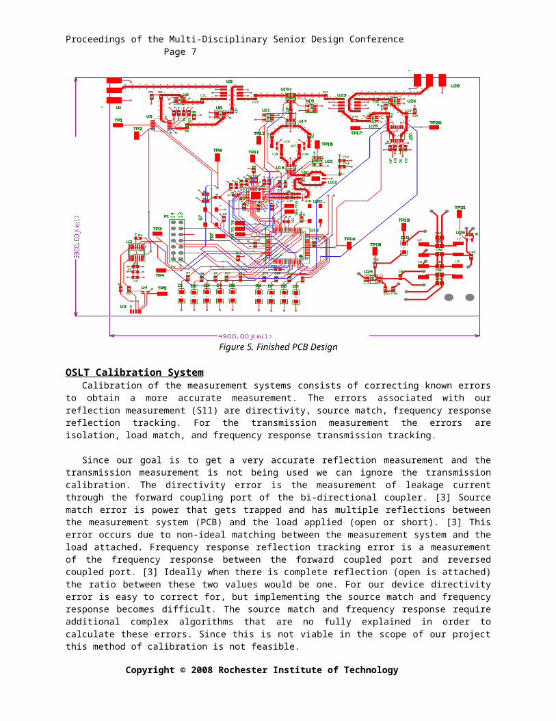
PCB DesignThe large frequency range our device required presented a challenge in regards to constructing the PCB. The
microstrip transmission lines on our board had to be designed for a specific frequency of operation. Any microstrip transmission line’s impedance changes with the frequency, therefore the lines were designed based around the antennas resonance. Using a network analyzer in pre-testing we were able to determined our reflection antenna had a resonance of 1.175 GHz. Hence, we then designed the PCB transmission lines with a 50Ω impedance at the frequency of operation. Using Agilent’s free TXLine calculator from the program AWR (“microwave office”) we designed the transmission lines. The board was designed to be manufactured on FR-4.
Figure 4. Transmission Line Width Calculation
Project P13071

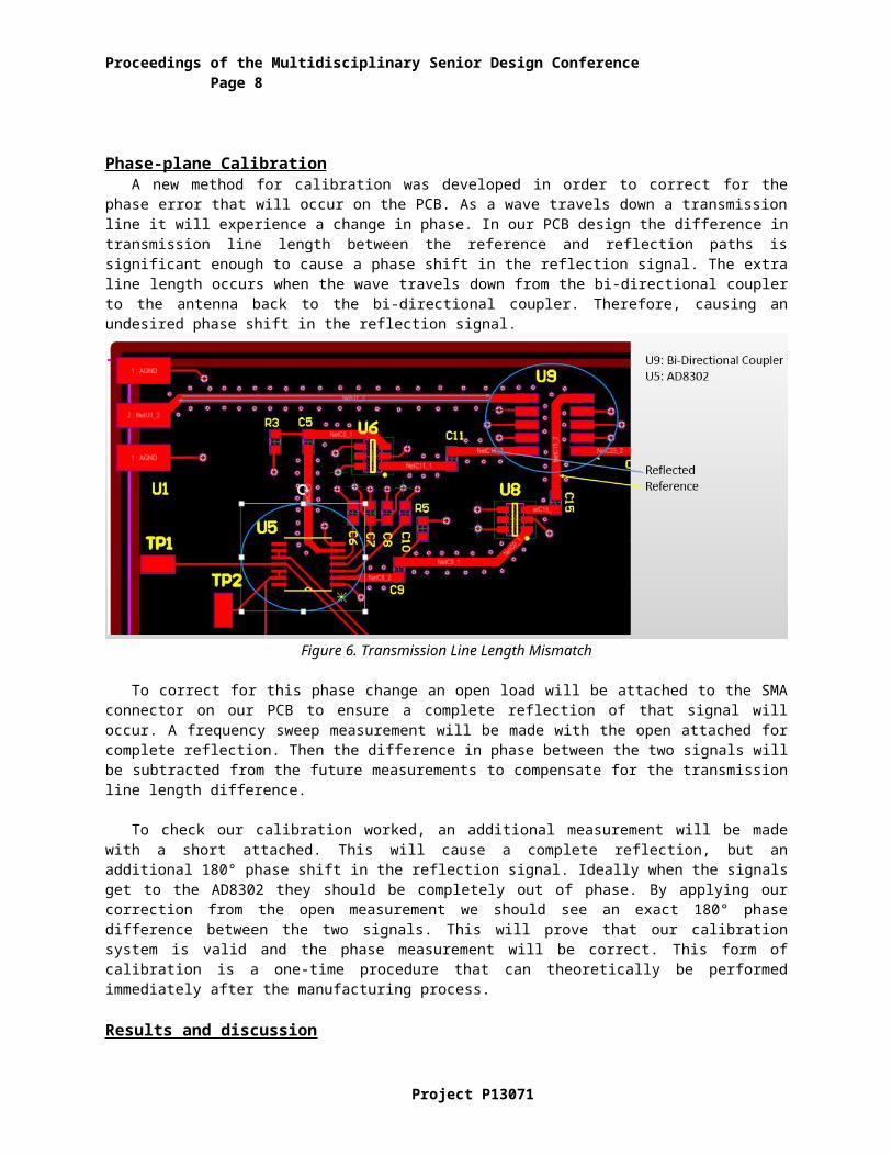
Proceedings of the Multi-Disciplinary Senior Design Conference Page 5
Figure 5. Finished PCB Design
OSLT Calibration SystemCalibration of the measurement systems consists of correcting known errors to obtain a more accurate
measurement. The errors associated with our reflection measurement (S11) are directivity, source match, frequency response reflection tracking. For the transmission measurement the errors are isolation, load match, and frequency response transmission tracking.
Since our goal is to get a very accurate reflection measurement and the transmission measurement is not being used we can ignore the transmission calibration. The directivity error is the measurement of leakage current through the forward coupling port of the bi-directional coupler. [3] Source match error is power that gets trapped and has multiple reflections between the measurement system (PCB) and the load applied (open or short). [3] This error occurs due to non-ideal matching between the measurement system and the load attached. Frequency response reflection tracking error is a measurement of the frequency response between the forward coupled port and reversed coupled port. [3] Ideally when there is complete reflection (open is attached) the ratio between these two values would be one. For our device directivity error is easy to correct for, but implementing the source match and frequency response becomes difficult. The source match and frequency response require additional complex algorithms that are no fully explained in order to calculate these errors. Since this is not viable in the scope of our project this method of calibration is not feasible.
Phase-plane CalibrationA new method for calibration was developed in order to correct for the phase error that will occur on the PCB.
As a wave travels down a transmission line it will experience a change in phase. In our PCB design the difference in transmission line length between the reference and reflection paths is significant enough to cause a phase shift in the reflection signal. The extra line length occurs when the wave travels down from the bi-directional coupler to the antenna back to the bi-directional coupler. Therefore, causing an undesired phase shift in the reflection signal.
Copyright © 2008 Rochester Institute of Technology
Proceedings of the Multidisciplinary Senior Design Conference Page 6
Figure 6. Transmission Line Length Mismatch
To correct for this phase change an open load will be attached to the SMA connector on our PCB to ensure a complete reflection of that signal will occur. A frequency sweep measurement will be made with the open attached for complete reflection. Then the difference in phase between the two signals will be subtracted from the future measurements to compensate for the transmission line length difference.
To check our calibration worked, an additional measurement will be made with a short attached. This will cause a complete reflection, but an additional 180° phase shift in the reflection signal. Ideally when the signals get to the AD8302 they should be completely out of phase. By applying our correction from the open measurement we should see an exact 180° phase difference between the two signals. This will prove that our calibration system is valid and the phase measurement will be correct. This form of calibration is a one-time procedure that can theoretically be performed immediately after the manufacturing process.
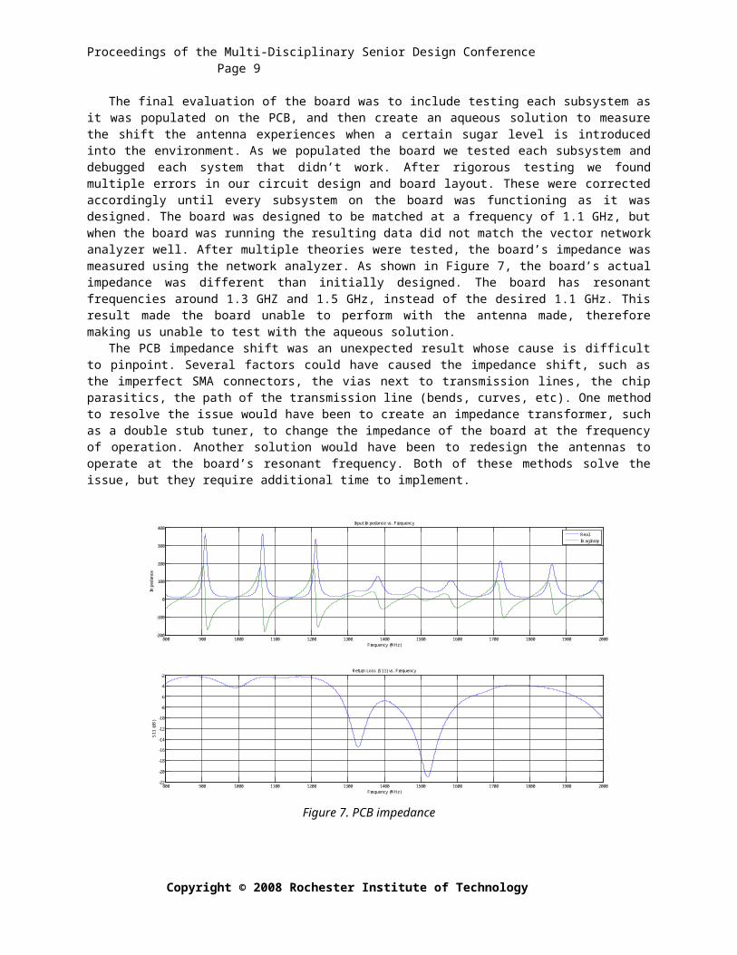
Results and discussionThe final evaluation of the board was to include testing each subsystem as it was populated on the PCB, and
then create an aqueous solution to measure the shift the antenna experiences when a certain sugar level is introduced into the environment. As we populated the board we tested each subsystem and debugged each system that didn’t work. After rigorous testing we found multiple errors in our circuit design and board layout. These were corrected accordingly until every subsystem on the board was functioning as it was designed. The board was designed to be matched at a frequency of 1.1 GHz, but when the board was running the resulting data did not match the vector network analyzer well. After multiple theories were tested, the board’s impedance was measured using the network analyzer. As shown in Figure 7, the board’s actual impedance was different than initially designed. The board has resonant frequencies around 1.3 GHZ and 1.5 GHz, instead of the desired 1.1 GHz. This result made the board unable to perform with the antenna made, therefore making us unable to test with the aqueous solution.
The PCB impedance shift was an unexpected result whose cause is difficult to pinpoint. Several factors could have caused the impedance shift, such as the imperfect SMA connectors, the vias next to transmission lines, the chip parasitics, the path of the transmission line (bends, curves, etc). One method to resolve the issue would have been to create an impedance transformer, such as a double stub tuner, to change the impedance of the board at the frequency of operation. Another solution would have been to redesign the antennas to operate at the board’s resonant frequency. Both of these methods solve the issue, but they require additional time to implement.
Project P13071
Proceedings of the Multi-Disciplinary Senior Design Conference Page 7
800 900 1000 1100 1200 1300 1400 1500 1600 1700 1800 1900 2000-200
-100
0
100
200
300
400Input Impedance vs. Frequency
Frequency (MHz)
Impe
danc
e
800 900 1000 1100 1200 1300 1400 1500 1600 1700 1800 1900 2000-22
-20
-18
-16
-14
-12
-10
-8
-6
-4
-2Return Loss (S11) vs. Frequency
Frequency (MHz)
S11
(dB
)
RealImaginary
Figure 7. PCB impedance
SoftwareThe MATLAB code running on a PC handled all of the data processing and displayed the results using a
GUI. MATLAB would tell the microcontroller a start frequency, stop frequency, and frequency step size before every measurement sweep. The microcontroller would then set the PLL to a frequency, wait for it to lock, sample the AD8302 outputs, and send the results to the PC. MATLAB then takes the AD8302 measurements from the microcontroller message and converts them to the reflection coefficient and input impedance of the antenna. The microcontroller then increments the frequency output by the PLL by the frequency step size, and the process repeats until the entire measurement sweep is finished.
The GUI depicted in Figure 8 describes the functionality of the MATLAB code. The bottom plot is a real time plot of the measurement results. It can display the S11 return loss, S21 return loss, or reflection antenna input impedance (real and imaginary components) in real time. The resonant frequency is then determined by searching for the minimum on the reflection antenna return loss pattern, and searching outward for a location where the imaginary portion of the antenna impedance is zero and the real portion is around 50Ω. This resonant frequency is then plotted on the top figure against the measurement time so the user can track the resonant frequency over time.
The MATLAB code can also implement a dynamic frequency ranging system, where a coarse resolution is used to find the resonant frequency, and a fine resolution is used to track it. The communication between the PC and microcontroller limits how many measurements can be taken by the board in a quick amount of time. In order to maintain a consistent measurement time the same number of measurements are taken each sweep, but the step size changes. The initial sweep has a large step size in order to locate the resonant frequency of the patient. After it’s located, the step size is reduced and the frequency sweep range is centered on the resonant frequency for the next sweep. The resonant frequency can then be tracked with high resolution without slowing down the measurement process. The calibrate button implements the phase-plane calibration described above.
Copyright © 2008 Rochester Institute of Technology
Proceedings of the Multidisciplinary Senior Design Conference Page 8
Figure 8. Matlab GUI
Conclusions and recommendationsOverall, each subsystem of the device was thoroughly tested and functioned as it was designed to, but the
unexpected shift in the board’s impedance made the device fail to perform its overall function. The evaluation boards for the MSP430 and ADF4351 were pivotal in trouble shooting the final board. Multiple errors were found in the initial design, but these were all corrected accordingly. Unfortunately, the impedance mismatch would require respinning the board or designing and manufacturing a new antenna, which would require resources beyond our initial allotment. In order to demonstrate the functionality of the automation code, the network analyzer was substituted for the developed PCB. The resulting data shows good agreement with the theoretical results in Figure 8, verifying the functionality of the developed code.
Recommendations:There are multiple avenues this project can be taken from its current state.
Case 1: Keep the same design, but resolve the issues we had with our board Redesign board for the correct impedance of the antenna.
o Simulate entire board using designer. Put S-parameters in for every element in order to verify impedance matching.
Or redesign the antenna to operate at the frequency the board naturally operates ato Antennas should be manufactured outside of RIT. In house production (machining, chemical
etching, etc.) might produce a functional antenna, but professional quality construction would remove this as a source of error.
Project P13071
Proceedings of the Multi-Disciplinary Senior Design Conference Page 9
Case 2: Redesign the board, but use the same overall functionality (PLL with AD8302) Buy the evaluation board for the AD8302 for the group to practice with
o Implement a system break out where the evaluation boards (ADF4351, AD8302, uC) are used to prove the overall system is functioning properly with the code created
Implement the 360° phase measurement method with two AD8302 chips Design the board to function at a certain resonant frequency and manufacture the board. After the board is
populated, measure where the board is actually resonating and design the antennas to match it.
Case 3: Look for new ways to implement a vector measurement system. Investigate a new method of recording a vector measurement outside of the AD8302 and I/Q demodulation.
o This option is research heavy, and might lead to a shortened product build/test cycle. o The resources from the current iteration of this project will not be useful (evaluation boards,
microcontroller code, etc.).
Skills required for next group: RF PCB design experience is highly recommended Group should have class experience in microwave circuit design One member should have an embedded programming focus. Training in the SMT lab. Some components were small enough to produce significant trouble during
population process.
General recommendations; Develop a robust communication system between the PC and microcontroller so information can be
transferred faster. Baud rate was limited to 9600 before bit errors threw off information exchange. Set up peripheral circuit components (power regulator, low battery indicator, etc.) that do not require
evaluation boards on a bread board to verify they work as well. Investigate implementing additional features such as wireless data transfer, on board memory, an LCD
display, etc. in addition to the current design.
References[1] C. Ziomek and P. Corredoura, “Digital I/Q demodulator,” in Proc. Particle Accelerator Conf., Dallas,
Texas, May 1995, vol. 4, pp. 2663–2665. [2] J. Flynn, S. Katz, and D. Schwartz. Csun.edu. California State University, Northridge, n.d. Web. 18 Apr.
2013. <http://www.csun.edu/~skatz/katzpage/sdr_project/sdr/IandQ%20_and_Sideband_7_10.pdf>.[3] "Measurement Errors." Measurement Errors. Agilent, n.d. Web. 08 Oct. 2013.
<http://na.tm.agilent.com/pna/help/latest/S3_Cals/Errors.htm>.[4] Jung, Jihak, Wooyoung Choi, and Jaehoon Choi. "A Small Wideband Microstrip-fed Monopole Antenna."
IEEE Microwave and Wireless Components Letters 15.10 (2005): 703-05. Print.[5] Freer, Benjamin. "Feasibility of a Non-Invasive Wireless Blood Glucose Monitor." Thesis. Rochester
Institute of Technology, 2011. Print.
AcknowledgmentsThis material is based upon the previous research performed by Dr. Venkataraman and Benjamin Freer for non-
invasive blood glucose monitors.
Copyright © 2008 Rochester Institute of Technology
Proceedings of the Multidisciplinary Senior Design Conference Page 10
Requirements and Advice
Copyright The copyright statement at the bottom of the first page allows RIT (the MSD program) to print your paper and make it available electronically. The authors maintain the right to submit the paper for publication elsewhere. You will be asked to sign an “offer of a technical paper” document which grants RIT rights under Copyright law. If this document is not signed, your technical paper cannot be published.
Project P13071