Problem Sheet 1 From material in Lectures 2 to 5d) Find a real solution for C. 3) Consider the...
27
Electrons in Solids (2012) Problem Sheet 1 From material in Lectures 2 to 5 1) [Standard derivation] Consider the free electron model for a 1- dimensional solid between x = 0 and x = L. For this model the time independent Schrödinger equation has the form: a) Write down the boundary conditions. b) Show that it has a general solution of the form: ψ( x) = A exp(ik x x ) and find values of wavevector k x . c) Find a real solution for A. d) Find the dispersion relationship. e) First consider only positive values of k x . Find the density of states D(E). f) How does this differ from D(E) for the 1-dimensional particle- in-a-box / infinite well model? g) Find the value for D(E) for the situation when both positive and negative values of k x are allowed. 2) Consider a nanoscale solid whose smallest sub-unit has length d. Treat the solid as a 1-dimensional infinite potential well containing non- interacting electrons. The nanoscale solid can increase its length according to L = pd, where p is an integer number of sub-units. Let each sub-unit contain 5 electrons. Find the variation of the smallest electronic transition ΔE with p for both p even and p odd, and show that at large p they both tend to: 3) For 2) above, find the general equation for the Fermi level E F for p even and p odd. If d = 0.5 nm, calculate the limiting value of E F (in eV) at large p. 4) In Lecture 3 we showed that the finite potential well lead to intermediate solutions of the form: in the three different regions. By considering the continuity of ψ and ψ’ at x = -a and +a, find the full even and odd solutions. − 2 2m d 2 dx 2 ψ = Eψ ΔE ≈ 5π 2 2 2mpd 2 ψ I ( x) = C exp(βx) ψ II ( x) = A cos( αx) + B sin( αx) ψ III ( x) = D exp(−βx) β 2 = 2m( V 0 − E ) 2 α 2 = 2mE 2
Transcript of Problem Sheet 1 From material in Lectures 2 to 5d) Find a real solution for C. 3) Consider the...
Electrons in Solids (2012)
Problem Sheet 1
From material in Lectures 2 to 5
1) [Standard derivation] Consider the free electron model for a 1-dimensional solid between x = 0 and x = L. For this model the time independent Schrödinger equation has the form:
a) Write down the boundary conditions. b) Show that it has a general solution of the form:
€
ψ(x) = Aexp(ikxx) and find values of wavevector kx.
c) Find a real solution for A. d) Find the dispersion relationship. e) First consider only positive values of kx. Find the density of
states D(E). f) How does this differ from D(E) for the 1-dimensional particle-
in-a-box / infinite well model? g) Find the value for D(E) for the situation when both positive
and negative values of kx are allowed.
2) Consider a nanoscale solid whose smallest sub-unit has length d. Treat the solid as a 1-dimensional infinite potential well containing non-interacting electrons. The nanoscale solid can increase its length according to L = pd, where p is an integer number of sub-units. Let each sub-unit contain 5 electrons. Find the variation of the smallest electronic transition ΔE with p for both p even and p odd, and show that at large p they both tend to:
3) For 2) above, find the general equation for the Fermi level EF for p even
and p odd. If d = 0.5 nm, calculate the limiting value of EF (in eV) at large p.
4) In Lecture 3 we showed that the finite potential well lead to
intermediate solutions of the form:
in the three different regions. By considering the continuity of ψ and ψ’ at x = -a and +a, find the full even and odd solutions.
€
−2
2md2
dx2 ψ = Eψ
€
ΔE ≈5π 22
2mpd2
€
ψI (x) = C exp(βx)ψII (x) = Acos(αx) + Bsin(αx)ψIII (x) = D exp(−βx)
€
β2 =2m(V0 −E)2
€
α2 =2mE2
Electrons in Solids (2012)
Problem Sheet 2
From material in Lectures 5 to 8
1) Electrons in solids obey Fermi-Dirac statistics. a) Define the Fermi energy EF. b) State the Fermi-Dirac distribution function, and sketch how it
varies with temperature. c) Define the chemical potential µ. d) What is the limit in which EF = µ? e) By considering the value of the Fermi temperature TF, is it
possible to approximate EF by µ at 300K? Sketch the room temperature Fermi-Dirac distribution for a typical metal according to the free electron model.
2) [Standard derivation] Consider the 3-dimensional free electron model (3D FEM) for a cube which lies between x = 0 and x = L, y = 0 and y = L and z = 0 and z = L, and has total volume V = L3. For this model the time independent Schrödinger equation has the form:
a) Write down the boundary conditions in terms of x, y and z. b) Show that it has a general solution of the form:
and find the dispersion relationship. c) Find the values of the wavevector components kx, ky and kz. d) Find a real solution for C.
3) Consider the 3-dimensional free electron model from question 2).
a) Find the volume occupied per state in k-space. b) By considering the number of states in a spherical shell in k-
space, find dn/dk. c) Hence find the density of states D(E). d) From D(E) and the answer to 1)a), find the Fermi energy EF. e) From the value of EF find the Fermi wavevector kF. f) By rewriting the answer to part 1)a) in terms of k instead of
E, find a second method to calculate kF. g) By considering a sphere in k-space occupied by N carriers,
find a third method to calculate kF. h) From 3)g) or h), find EF, and hence D(E).
4) How does the 3-dimensional free electron model explain the
electrical conductivity σ (Ωm) of metals? Consider both the charge carrier density and the charge carrier mobility.
€
−2
2m∇2ψ = Eψ
€
ψ(r ) = C exp(ik.r )
Electrons in Solids (2012)
Problem Sheet 3
From material in Lectures 8 to 12
1) For the 3-dimensional free electron model (3D FEM) it is possible to calculate a fundamental thermal property of solids, the specific heat.
a) Give a simple definition of the specific heat CV. Write down equations for it in units of J K-1, J K-1 mol-1 and J K-1 kg-1.
b) What is CV (J K-1) for a classical ideal gas of N particles? c) Consider the 3D FEM for a cube of volume V containing N
electrons. Find the thermal energy ΔU of the electrons within kTB of the surface of the Fermi sphere.
d) Using the values of D(E) and EF, show that for the 3D FEM:
€
D(EF ) =3N2EF
e) Hence, find the 3D FEM specific heat CV (J K-1). How does this and the answer to 1)b) compare to the measured CV for metals at low temperatures?
2) What method can be used to measure the Fermi surfaces of real
metals? Do these Fermi surfaces differ from that predicted by the 3D FEM? What are the successes and failures of the FEM?
3) A 1-dimensional (1D) periodic potential has the form:
a) State Bloch’s theorem for this potential. b) How is the Bloch wavefunction ψ(x) related to itself in the
nearest-neighbour unit cell (ie. when n = 1)? c) Show that the wavefunction is equally distributed in both unit
cells. d) What are the allowed wavevector kx values for these states. e) How does the meaning of kx differ from that in the 1D FEM.
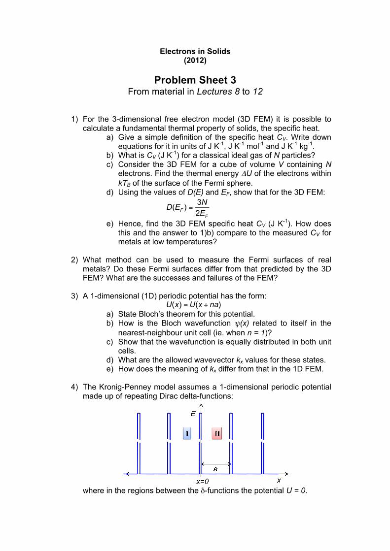
4) The Kronig-Penney model assumes a 1-dimensional periodic potential
made up of repeating Dirac delta-functions:
where in the regions between the δ-functions the potential U = 0.
€
U(x) = U(x + na)
4) continued
a) In unit cell I, a trial solution ψΙ(x) has the form of an incident and reflected traveling wave:
€
ψI (x) = An exp(−iqx) + Bn exp(iqx)
Rewrite this in the form of Csin(qx) and Dcos(qx), and find a value for q.
b) Using Bloch’s theorem, write down a solution for the wavefunction ψΙΙ(x) in unit cell II.
c) Using continuity at x = 0, find an equation relating ψΙ(x) to ψΙΙ(x).
d) Show that this leads to:
€
CD
=cos(qa) −exp(−ikxa)
sin(qa)
e) Find the first derivative with x of ψΙ(x) and ψΙΙ(x). f) Using the Dirac delta-function (cusp) condition at x = 0:
€
∂ψII (0)∂x
−∂ψI (0)∂x
=2mU0
2 ψI (0)
find an equation relating dψΙ(x)/dx to dψΙΙ(x)/dx. g) Shows that this leads to:
€
CD
=exp(ikxa) sin(qa) −2mU0 q2
1−exp(ikxa) cos(qa)
h) Using d) and g), find the Kronig-Penney equation:
€
cos(kxa) = cos(qa) +maU0
2
sin(qa)qa
5) Consider the Kronig-Penney model in question 4).
a) Sketch the variation of the right hand side of the Kronig-Penney equation:
€
cos(qa) +maU0
2
sin(qa)qa
with qa for both U0 = 0 and U0 > 0. b) Sketch the Kronig-Penney dispersion curve and compare it
to that of the1D FEM. At what kx values do discontinuities occur in energy?
c) How many states are there per energy band? d) What is the variation of the chemical potential with number of
electrons per unit cell?
Electrons in Solids (2012)
Problem Sheet 4
From material in Lectures 12 to 17
1) Consider the Kronig-Penny band theory model. a) Sketch the Kronig-Penney dispersion curve showing the 1st
to 4th energy bands and the 1st to 4th Brillouin zones. b) All Bloch wavefunction wavevector values k’ outside the 1st
Brillouin zone (BZ) can be translated into it using the equation:
where n’ is an integer and k lies inside the 1st BZ. Find the values for n’ when k’ lies inside the 2nd, 3rd and 4th BZ for both positive and negative k’.
c) Sketch the extended, periodic and reduced zone schemes.
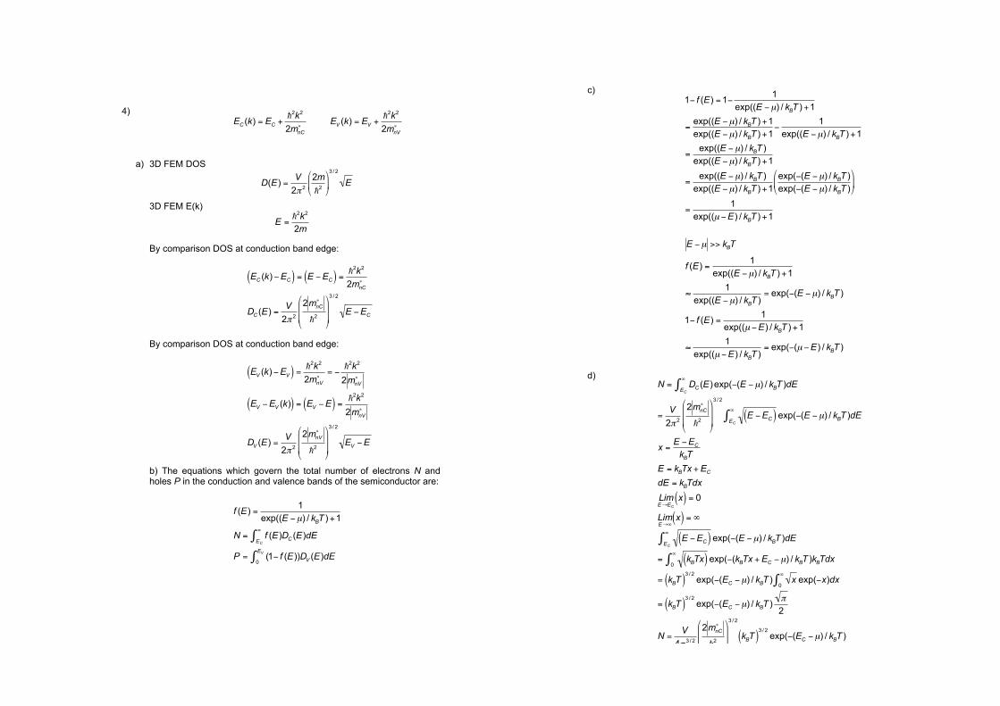
2) Sketch the band structure of a semiconductor in real space and in k-space, the latter using the reduced zone scheme representation, showing the energies of the conduction band minima EC and valence band maxima EV, the energy gap EG and the chemical potential µ.
3) The Kronig-Penney dispersion relationship has the form:
€
cos(kxa) = cos(qa) +maU0
2
sin(qa)qa
where symbols have their usual meaning. Show that when U0 and kx, and therefore E, are small the effective mass m* is given by:
4) The conduction and valence band dispersion curves EC(k) and EV(k) of a semiconductor at the edge of the energy gap can be closely approximated by:
where symbols have there usual meaning. a) By considering the density of states (DOS) for the 3D free
electron model, write down equations for the DOS in the semiconductor at the conduction and valence band edges.
€
′ k = k +2πa
′ n
€
m* = m maU0
32 +1
€
EC (k) = EC +
2k2
2mnC∗
€
EV (k) = EV +
2k2
2mnV∗
b) What are the equations which govern the total number of electrons N and holes P in the conduction and valence bands of the semiconductor?
c) Show that for |E-µ| >> kBT, the Fermi-Dirac distribution function for the occupied states in the conduction band and the unoccupied states in the valence band are given respectively by:
d) Using the integral: and appropriate substitutions, show that the electron and hole carrier densities are given by: and find values of NC and NV.
5) Using sketches of the band diagrams in real space, explain the difference between an intrinsic, a p-type extrinsic and a n-type extrinsic semiconductor.
€
f (E) = exp(−(E −µ) / kBT )1− f (E) = exp(−(µ −E) / kBT )
€
x exp(−x)dx0
∞
∫ =π2
€
n = NC exp(−(EC −µ) / kBT )p = NV exp(−(µ −EV ) / kBT )
Electrons in Solids (2012)
Problem Sheet 1
SOLUTIONS Covering material in Lectures 2 to 5
1) a) 1D Born von Karman boundary conditions:-
b)
€
ψ(x) = Aexp(ikxx)
Allow both positive & negative values of kx
n = ±1, ±2, ±3, ±4,……
c) If both positive & negative values of kx:
€
ψ(x) =ψ(x + L)
€
−2
2md 2ψdx2
= Eψ
€
2
2mkx
2ψ = Eψ
E =2kx
2
2m
€
ψ(x) =ψ(x + L)ψ(0) =ψ(0 + L)A = Aexp(ikxL)kxL = 2πn
kx =2πnL
€
E =2kx
2
2mk = kx
k =2m2
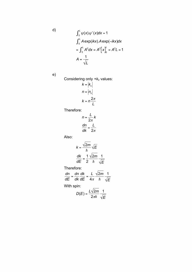
d) e)
Considering only +kx values:
Therefore:
Also:
Therefore:
With spin:
€
k = kx
n = nx
k = n 2πL
€
ψ(x).ψ∗(x)0
L∫ dx = 1
Aexp(ikx).Aexp(−ikx)0
L∫ dx
= A20
L∫ dx = A2 x[ ]0
L= A2L = 1
A =1L
€
n =L
2πk
dndk
=L
2π
€
k =2m
E
dkdE
=12
2m
1E
€
dndE
=dndk
dkdE
=L
4π2m
1E
€
D(E) =L 2m2π
1E
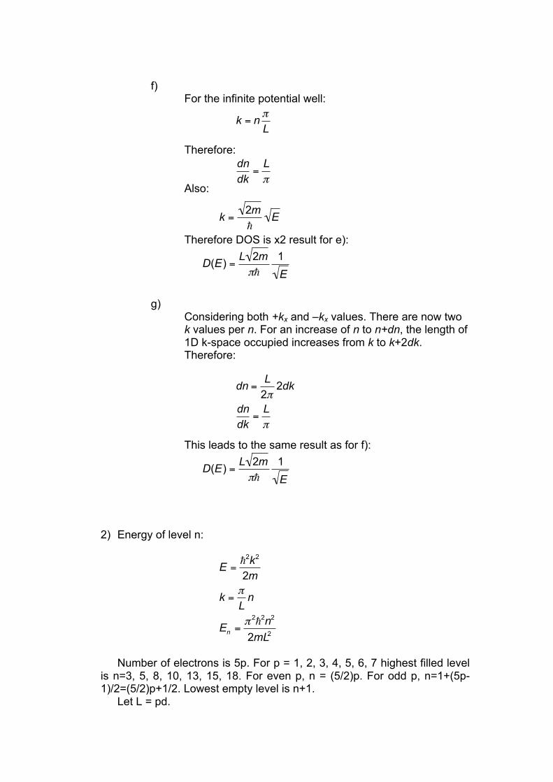
f)
For the infinite potential well:
Therefore:
Also: Therefore DOS is x2 result for e):
g)
Considering both +kx and –kx values. There are now two k values per n. For an increase of n to n+dn, the length of 1D k-space occupied increases from k to k+2dk. Therefore:
This leads to the same result as for f):
2) Energy of level n:
Number of electrons is 5p. For p = 1, 2, 3, 4, 5, 6, 7 highest filled level is n=3, 5, 8, 10, 13, 15, 18. For even p, n = (5/2)p. For odd p, n=1+(5p-1)/2=(5/2)p+1/2. Lowest empty level is n+1. Let L = pd.
€
D(E) =L 2mπ
1E
€
k = n πL
€
dndk
=Lπ
€
k =2m
E
€
dn =L
2π2dk
dndk
=Lπ
€
D(E) =L 2mπ
1E
€
E =2k2
2m
k =πL
n
En =π 22n2
2mL2
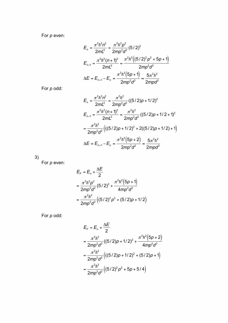
For p even:
For p odd: 3)
For p even:
For p odd:
€
En =π 22n2
2mL2=π 22p2
2mp2d2(5 / 2)2
En +1 =π 22(n +1)2
2mL2 =π 22 (5 / 2)2 p2 + 5p +1( )
2mp2d2
ΔE = En +1 −En =π 22 5p +1( )
2mp2d2 ≈5π 22
2mpd2
€
En =π 22n2
2mL2=
π 22
2mp2d2((5 / 2)p +1/ 2)2
En +1 =π 22(n +1)2
2mL2=
π 22
2mp2d2((5 / 2)p +1/ 2 +1)2
=π 22
2mp2d2((5 / 2)p +1/ 2)2 + 2((5 / 2)p +1/ 2) +1( )
ΔE = En +1 −En =π 22 5p + 2( )
2mp2d2 ≈5π 22
2mpd2
€
EF = En +ΔE2
=π 22p2
2mp2d2 (5 / 2)2 +π 22 5p +1( )
4mp2d2
=π 22
2mp2d2 (5 / 2)2 p2 + (5 / 2)p +1/ 2( )
€
EF = En +ΔE2
=π 22
2mp2d2((5 / 2)p +1/ 2)2 +
π 22 5p + 2( )4mp2d2
=π 22
2mp2d2((5 / 2)p +1/ 2)2 + (5 / 2)p +1( )
=π 22
2mp2d2(5 / 2)2 p2 + 5p + 5 / 4( )
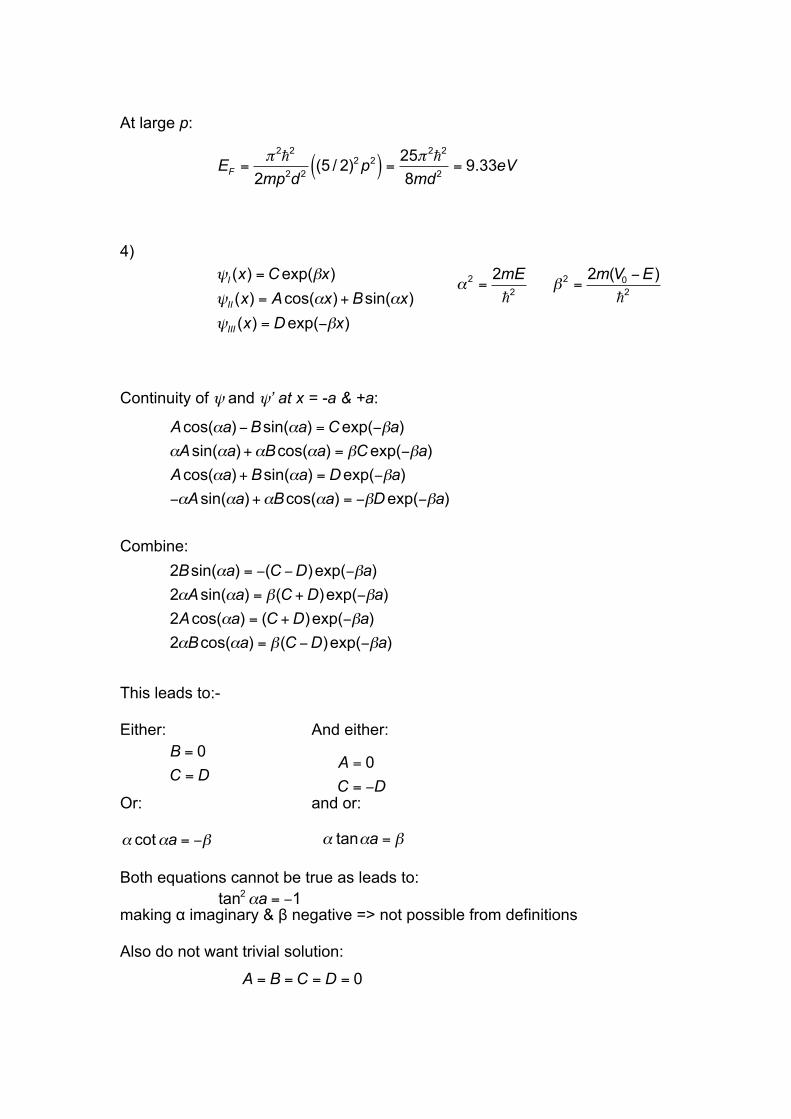
At large p: 4) Continuity of ψ and ψ’ at x = -a & +a: Combine: This leads to:- Either: And either: Or: and or:
€
α tanαa = β Both equations cannot be true as leads to:
€
tan2αa = −1 making α imaginary & β negative => not possible from definitions Also do not want trivial solution:
€
EF =π 22
2mp2d2 (5 / 2)2 p2( ) =25π 22
8md2 = 9.33eV
€
2Bsin(αa) = −(C −D)exp(−βa)2αAsin(αa) = β(C + D)exp(−βa)2Acos(αa) = (C + D)exp(−βa)2αBcos(αa) = β(C −D)exp(−βa)
€
ψI (x) = C exp(βx)ψII (x) = Acos(αx) + Bsin(αx)ψIII (x) = D exp(−βx)
€
Acos(αa) −Bsin(αa) = C exp(−βa)αAsin(αa) +αBcos(αa) = βC exp(−βa)Acos(αa) + Bsin(αa) = D exp(−βa)−αAsin(αa) +αBcos(αa) = −βD exp(−βa)
€
B = 0C = D
€
A = 0C = −D
€
α cotαa = −β
€
A = B = C = D = 0
€
β2 =2m(V0 −E)2
€
α2 =2mE2
Therefore we have two possible solution sets: Either: Or:
€
α tanαa = β Leads to a set of even solutions:
€
α tanαa = β And odd solutions:
To solve the dispersion relationship then requires a graphical solution. Note: I would not require you to do the graphical solution under exam conditions. Note: The most important part of the above solution is to understand how the exponential tails in regions I and III leads to an extended wavefunction and tunnelling across the short distances between nano-scale solids, and how this tunnelling distance relates to mobility.
€
B = 0C = D
€
A = 0C = −D
€
α cotαa = −β
€
ψI (x) = C exp(βx)ψII (x) = Acos(αx)ψIII (x) = C exp(−βx)
€
ψI (x) = C exp(βx)ψII (x) = Bsin(αx)ψIII (x) = −C exp(−βx)
€
α cotαa = −β
Electrons in Solids (2012)
Problem Sheet 2
SOLUTIONS Covering material in Lectures 5 to 8
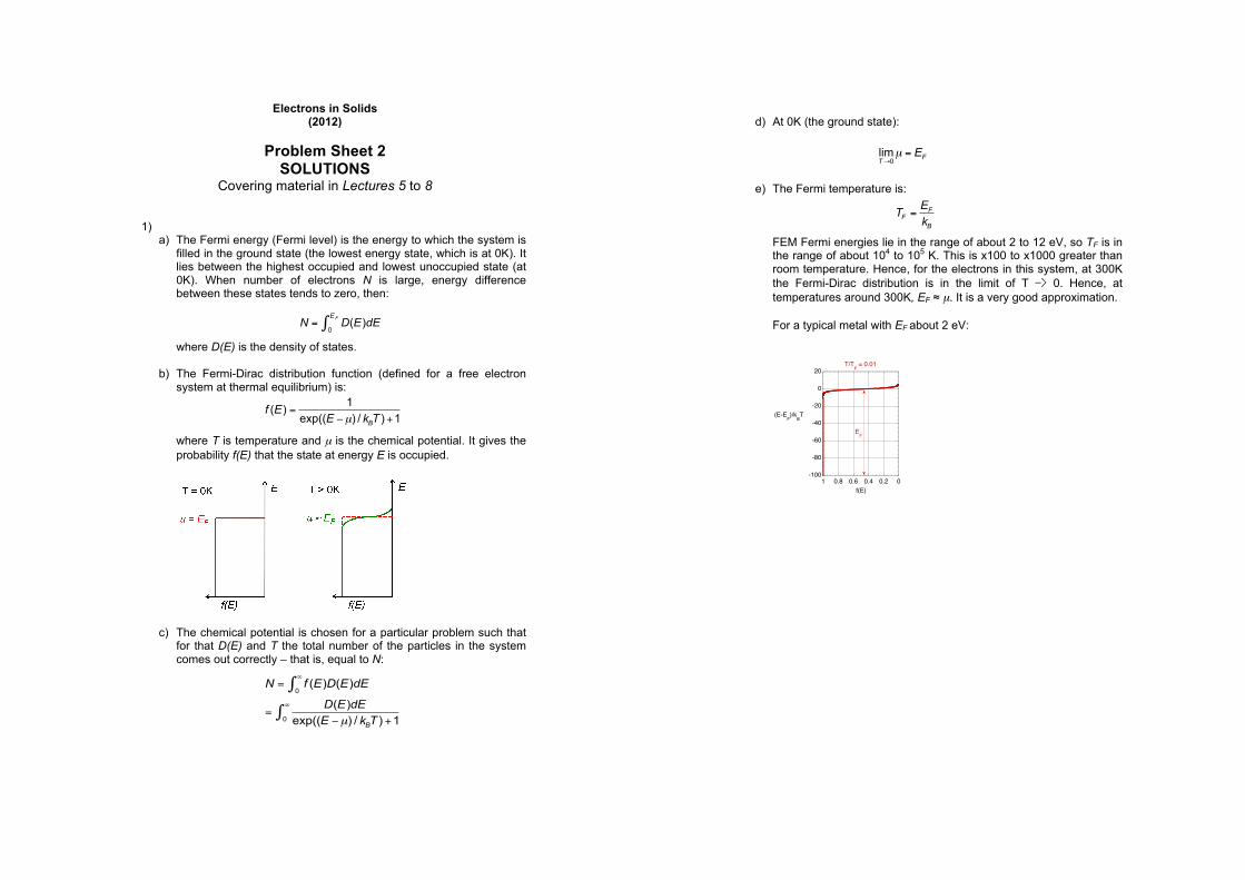
1) a) The Fermi energy (Fermi level) is the energy to which the system is
filled in the ground state (the lowest energy state, which is at 0K). It lies between the highest occupied and lowest unoccupied state (at 0K). When number of electrons N is large, energy difference between these states tends to zero, then:
where D(E) is the density of states.
b) The Fermi-Dirac distribution function (defined for a free electron system at thermal equilibrium) is: where T is temperature and µ is the chemical potential. It gives the probability f(E) that the state at energy E is occupied.
c) The chemical potential is chosen for a particular problem such that for that D(E) and T the total number of the particles in the system comes out correctly – that is, equal to N:
!
N = D(E)dE0
EF"
!
f (E) =1
exp((E "µ) / kBT ) +1
!
N = f (E)D(E)dE0
"
#
=D(E)dE
exp((E $µ) / kBT ) +10
"
#
d) At 0K (the ground state):
e) The Fermi temperature is: FEM Fermi energies lie in the range of about 2 to 12 eV, so TF is in the range of about 104 to 105 K. This is x100 to x1000 greater than room temperature. Hence, for the electrons in this system, at 300K the Fermi-Dirac distribution is in the limit of T -> 0. Hence, at temperatures around 300K, EF ! µ. It is a very good approximation. For a typical metal with EF about 2 eV:
-100
-80
-60
-40
-20
0
20
00.20.40.60.81
T/TF = 0.01
(E-EF)/k
BT
f(E)
EF
!
limT"0
µ = EF
!
TF =EF
kB
2)
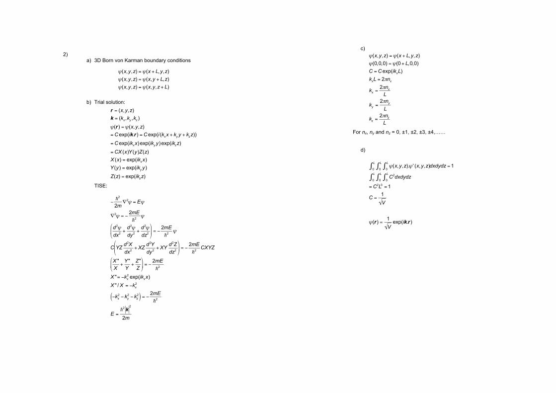
a) 3D Born von Karman boundary conditions
b) Trial solution:
TISE:
!!!!
!
!
"(x,y,z) ="(x + L,y,z)"(x,y,z) ="(x,y + L,z)"(x,y,z) ="(x,y,z + L)
!
r = (x,y,z)k = (kx,ky ,kz )
"(r ) ="(x,y,z)= C exp(ik.r ) = C exp(i (kxx + ky y + kzz))
= C exp(ikxx)exp(iky y)exp(ikzz)
= CX (x)Y (y)Z(z)X (x) = exp(ikxx)Y (y) = exp(iky y)
Z(z) = exp(ikzz)
!
"!2
2m#2$ = E$
#2$ = "2mE!2
$
d2$
dx2+
d2$
dy2+
d2$
dz2
%
& '
(
) * = "
2mE!2
$
C YZ d2Xdx2
+ XZ d2Ydy2
+ XY d2Zdz2
%
& '
(
) * = "
2mE!2
CXYZ
X "X
+Y "Y
+Z"Z
%
& '
(
) * = "
2mE!2
X "= "kx2 exp(ikxx)
X " / X = "kx2
"kx2 " ky
2 " kz2( ) = "
2mE!2
E =!2 k
2
2m
c)
For nx, ny and nz = 0, ±1, ±2, ±3, ±4,……
d)
!
"(x,y,z) ="(x + L,y,z)"(0,0,0) ="(0 + L,0,0)C = C exp(ikxL)kxL = 2#nx
kx =2#nx
L
ky =2#ny
L
kz =2#nz
L
!
"(x,y,z)."#(x,y,z)0
L$ dxdydz
0
L$0
L$ = 1
C20
L$ dxdydz
0
L$0
L$= C2L3 = 1
C =1V
!
"(r ) =1
Vexp(ik.r )
3)
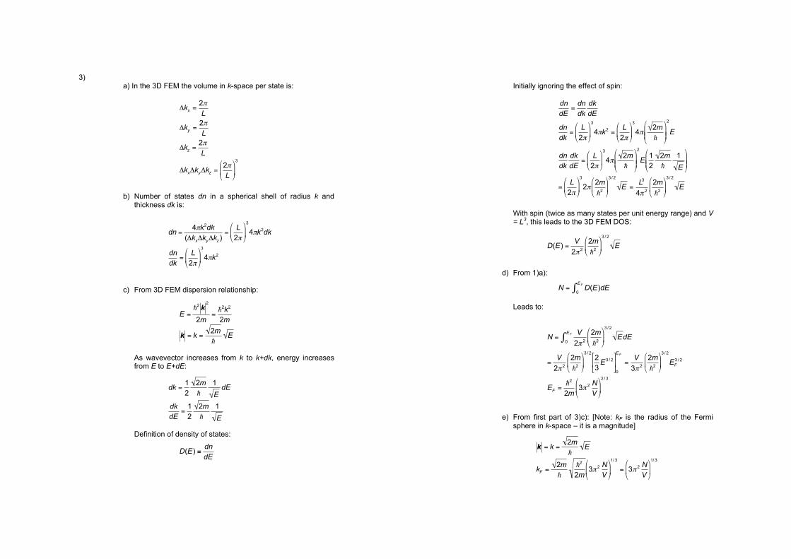
a) In the 3D FEM the volume in k-space per state is: b) Number of states dn in a spherical shell of radius k and
thickness dk is:
c) From 3D FEM dispersion relationship: As wavevector increases from k to k+dk, energy increases from E to E+dE: Definition of density of states:
!
"kx =2#L
"ky =2#L
"kz =2#L
"kx"ky"kz =2#L
$
% &
'
( )
3
!
dn =4"k2dk
(#kx#ky#kz )=
L2"$
% &
'
( )
3
4"k2dk
dndk
=L
2"$
% &
'
( )
3
4"k2
!
dk =12
2m!
1E
dE
dkdE
=12
2m!
1E
!
E =!2 k
2
2m=!2k2
2m
k = k =2m!
E
!
D(E) " dndE
Initially ignoring the effect of spin: With spin (twice as many states per unit energy range) and V = L3, this leads to the 3D FEM DOS:
d) From 1)a):
Leads to:
e) From first part of 3)c): [Note: kF is the radius of the Fermi sphere in k-space – it is a magnitude]
!
dndE
=dndk
dkdE
dndk
=L
2"#
$ %
&
' (
3
4"k2 =L
2"#
$ %
&
' (
3
4" 2m!
#
$ % %
&
' ( (
2
E
dndk
dkdE
=L
2"#
$ %
&
' (
3
4" 2m!
#
$ % %
&
' ( (
2
E 12
2m!
1E
#
$ % %
&
' ( (
=L
2"#
$ %
&
' (
3
2" 2m!2
#
$ %
&
' (
3 / 2
E =L3
4" 2
2m!2
#
$ %
&
' (
3 / 2
E
!
D(E) =V
2" 2
2m!2
#
$ %
&
' (
3 / 2
E
!
N = D(E)dE0
EF"
!
N =V
2" 2
2m!2
#
$ %
&
' (
3 / 2
EdE0
EF)
=V
2" 2
2m!2
#
$ %
&
' (
3 / 223
E3 / 2*
+ ,
-
. /
0
EF
=V
3" 2
2m!2
#
$ %
&
' (
3 / 2
EF3 / 2
EF =!2
2m3" 2 N
V
#
$ %
&
' (
2 / 3
!
k = k =2m!
E
kF =2m!
!2
2m3" 2 N
V#
$ %
&
' (
1/ 3
= 3" 2 NV
#
$ %
&
' (
1/ 3
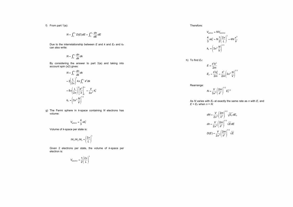
f) From part 1)a): Due to the interrelationship between E and k and EF and kF can also write: By considering the answer to part 3)a) and taking into account spin (x2) gives:
g) The Fermi sphere in k-space containing N electrons has volume: Volume of k-space per state is: Given 2 electrons per state, the volume of k-space per electron is:
!
N = D(E)dE0
EF" =dndE
dE0
EF"
!
N =dndk
dk0
k F"
!
N =dndk
dk0
k F"
= 2 L2#$
% &
'
( )
3
4# k2dk0
k F"
= 8# L2#$
% &
'
( )
3k3
3
*
+ ,
-
. /
0
k F
=V
3# 2 kF3
kF = 3# 2 NV
$
% &
'
( )
1/ 3
!
Vsphere =43"kF
3
!
"kx"ky"kz =2#L
$
% &
'
( )
3
!
Velectron =12
2"L
#
$ %
&
' (
3
Therefore:
h) To find EF: Rearrange: As N varies with EF at exactly the same rate as n with E, and E = EF when n = N:
!
Vsphere = NVelectron
43"kF
3 = N12
2"L
#
$ %
&
' (
3
= 4N" 3
V
kF = 3" 2 NV
#
$ %
&
' (
2 / 3
!
E =!2k2
2m
EF =!2kF
2
2m=!2
2m3" 2 N
V#
$ %
&
' (
2 / 3
!
N =V
3" 2
2m!2
#
$ %
&
' (
3 / 2
EF3 / 2
!
dN =V
2" 2
2m!2
#
$ %
&
' (
3 / 2
EF dEF
dn =V
2" 2
2m!2
#
$ %
&
' (
3 / 2
EdE
D(E) =V
2" 2
2m!2
#
$ %
&
' (
3 / 2
E
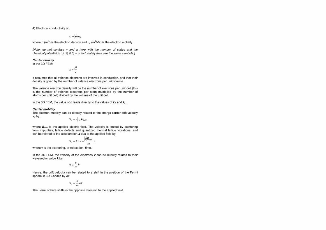
4) Electrical conductivity is: where n (m-3) is the electron density and µn (m2/Vs) is the electron mobility. [Note: do not confuse n and µ here with the number of states and the chemical potential in 1), 2) & 3) – unfortunately they use the same symbols.] Carrier density In the 3D FEM: It assumes that all valence electrons are involved in conduction, and that their density is given by the number of valence electrons per unit volume. The valence electron density will be the number of electrons per unit cell (this is the number of valence electrons per atom multiplied by the number of atoms per unit cell) divided by the volume of the unit cell. In the 3D FEM, the value of n leads directly to the values of EF and kF. Carrier mobility The electron mobility can be directly related to the charge carrier drift velocity vd by: where Efield is the applied electric field. The velocity is limited by scattering from impurities, lattice defects and quantized thermal lattice vibrations, and can be related to the acceleration a due to the applied field by: where ! is the scattering, or relaxation, time. In the 3D FEM, the velocity of the electrons v can be directly related to their wavevector value k by: Hence, the drift velocity can be related to a shift in the position of the Fermi sphere in 3D k-space by !k. The Fermi sphere shifts in the opposite direction to the applied field.
!
" = e nµn
!
n =NV
!
vd = "µn Efield
!
vd =!m"k
!
v =!m
k
!
vd = a" = #e Efield
m"
Electrons in Solids (2012)
Problem Sheet 3
SOLUTIONS From material in Lectures 8 to 12
1) a) The specific heat CV is the change in the internal energy U for a given change in temperature T at constant volume V. For an arbitrary system (eg. of N particles) this is:
!
CV ="U"T
#
$ %
&
' (
V
in units of J K-1. For a mole of material:
!
CV =1
NA
"U"T
#
$ %
&
' (
V
where NA is Avagadros number and CV is in units of J K-1 mol-1. For a mass m of material:
!
CV =1m
"U"T
#
$ %
&
' (
V
and cV is in units of J K-1 kg-1. b) For a classical ideal gas of N particles:
!
U =32
NkBT
CV =32
NkB
c) Width of region of thermally excited electrons at surface of Fermi sphere:
!
"E # kBT Density of states dn/dE at surface of sphere is D(EF). Therefore, number of thermally excited electrons at surface is:
As each of these electrons acquires thermal energy kBT, internal energy is therefore:
!
"U = nkT .kBT = D(EF ) kBT( )2
!
nkT = D(EF )"E= D(EF )kBT
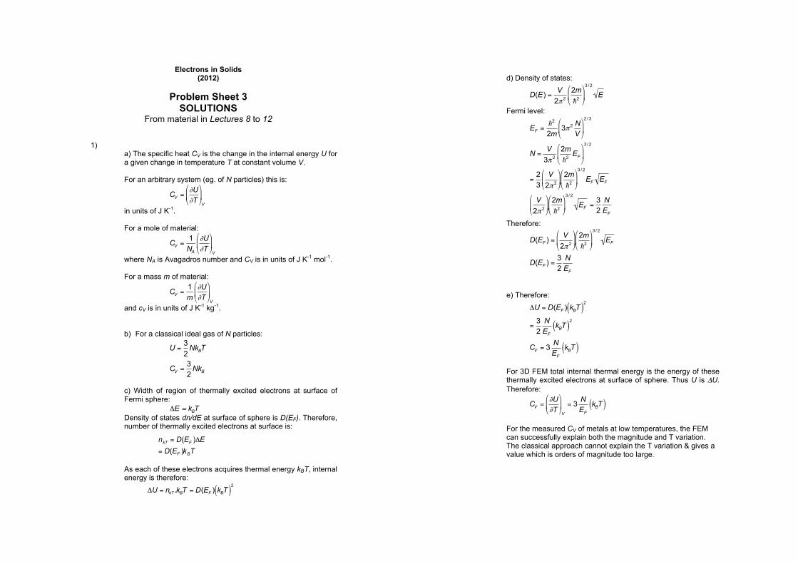
d) Density of states:
!
D(E) =V
2" 2
2m!2
#
$ %
&
' (
3 / 2
E
Fermi level:
!
EF =!2
2m3" 2 N
V#
$ %
&
' (
2 / 3
N =V
3" 2
2m!2 EF
#
$ %
&
' (
3 / 2
=23
V2" 2
#
$ %
&
' (
2m!2
#
$ %
&
' (
3 / 2
EF EF
V2" 2
#
$ %
&
' (
2m!2
#
$ %
&
' (
3 / 2
EF =32
NEF
Therefore:
!
D(EF ) =V
2" 2
#
$ %
&
' (
2m!2
#
$ %
&
' (
3 / 2
EF
D(EF ) =32
NEF
e) Therefore:
!
"U = D(EF ) kBT( )2
=32
NEF
kBT( )2
CV = 3 NEF
kBT( )
For 3D FEM total internal thermal energy is the energy of these thermally excited electrons at surface of sphere. Thus U is !U. Therefore:
!
CV ="U"T
#
$ %
&
' (
V
= 3 NEF
kBT( )
For the measured CV of metals at low temperatures, the FEM can successfully explain both the magnitude and T variation. The classical approach cannot explain the T variation & gives a value which is orders of magnitude too large.
2) Fermi surfaces of real metals can be measured using the de Haas – van Alphen effect. This measures oscillations, at low temperatures, of the magnetic susceptibility with magnetic field strength. The magnetic field results in quantized electron orbitals - a series of concentric cylinders in k-space known as Landau levels. If one of these intersects the belly of the Fermi sphere, it will produce a strong response. As the B-field increases, the cylinders contract, resulting in the oscillations as they pass through the sphere belly. Can be used to measure the area of the Fermi surface perpendicular to B. By changing direction of field can map out Fermi surface in 3D Real Fermi surfaces for some metals (alkali metals) do indeed have an approximately spherical Fermi surface, which is a key prediction of the 3D FEM. This indicates that the states are only weakly perturbed by the periodic lattice potentials. However, other Fermi surfaces differ radically, involving more than one non-spherical surface as well as having enclosed cavities in which holes can also orbit. The FEM successfully predicts the filling of the states in k-space and the existence of Fermi surfaces in metals. It also successfully explains the general electrical and thermal properties of metals. However, it cannot explain the detailed behaviour of many metals. Crucially, it also cannot explain the existence of semiconductors and semiconductors – it predicts that everything is a metal.
3)
a) Potential is in 1D, so Bloch’s Theorem 1D Periodic potential: Bloch’s Theorem: The eigenstates of the one electron Hamiltonian for a periodic potential can be chosen to have the form of a plane wave multiplied by a function with the periodicity of the lattice:
!
"(x) = uk (x)exp(ikxx) where:
!
uk (x) = uk (x + na) for all n.
!
U(x) = U(x + na)
b)
!
"(x + a) = uk (x + a)exp(ikx (x + a))="(x)exp(ikxa)
c)
!
"#(x + a)."(x + a)
="#(x)exp($ikxa)."(x)exp(ikxa)
="#(x)."(x)
%"#(x + a)."(x + a) = "#(x)."(x)
d) 1D BvK:
!
"(x + L) ="(x) For N unit cells:
!
L = Na"(x + Na) ="(x)exp(ikxNa)"(x + L) ="(x)exp(ikxL) ="(x)exp(ikxL) = 1
kx =2#L
nx
nx = ±1,±2,±3,...
(assuming kx can have both positive and negative values)
e) For a 1D Bloch wavefunction kx is the quantum number of that state. The wavefunction is a wavepacket constructed from different k values. kx is the wavevector value for the plane wave part of the wavefunction. It cannot be directly related to momentum p and velocity v. For a 1D FEM state the value of kx is also the quantum number of that state. As the wavefunction is a plane wave, kx is also the actual wavevector value of that state. kx can be directly related to momentum p and velocity v.
4) a)
!
"I (x) = An exp(#iqx) + Bn exp(iqx)= (#An + Bn ) sin(qx) + i (An + Bn ) cos(qx)= C sin(qx) + D cos(qx)
In regions between !–functions, U(x) = 0 so:
!
"!2
2m#$I (x)#x
= E$I (x)
"!2
2m"q2$I (x)( ) = E$I (x)
E =!2q2
2m
q =2mE!
b)
Bloch:
!
"(x + na) = exp(ikxna)"(x) So:
!
"II (x + a) = exp(ikxa)"I (x)
= exp(ikxa) C sin(qx) + D cos(qx)( )
Leads to:
!
"II (x) = exp(ikxa) C sin(q(x #a)) + D cos(q(x #a))( )
c) Continuity at x = 0
!
C sin(qx) + D cos(qx) = exp(ikxa) C sin(q(x "a)) + D cos(q(x "a))( )D = exp(ikxa) "C sin(qa) + D cos(qa)( )
!
!d)
!
1= exp(ikxa) "CD
sin(qa) + cos(qa)#
$ %
&
' (
exp("ikxa) " cos(qa) = "CD
sin(qa)
CD
=cos(qa) "exp("ikxa)
sin(qa)
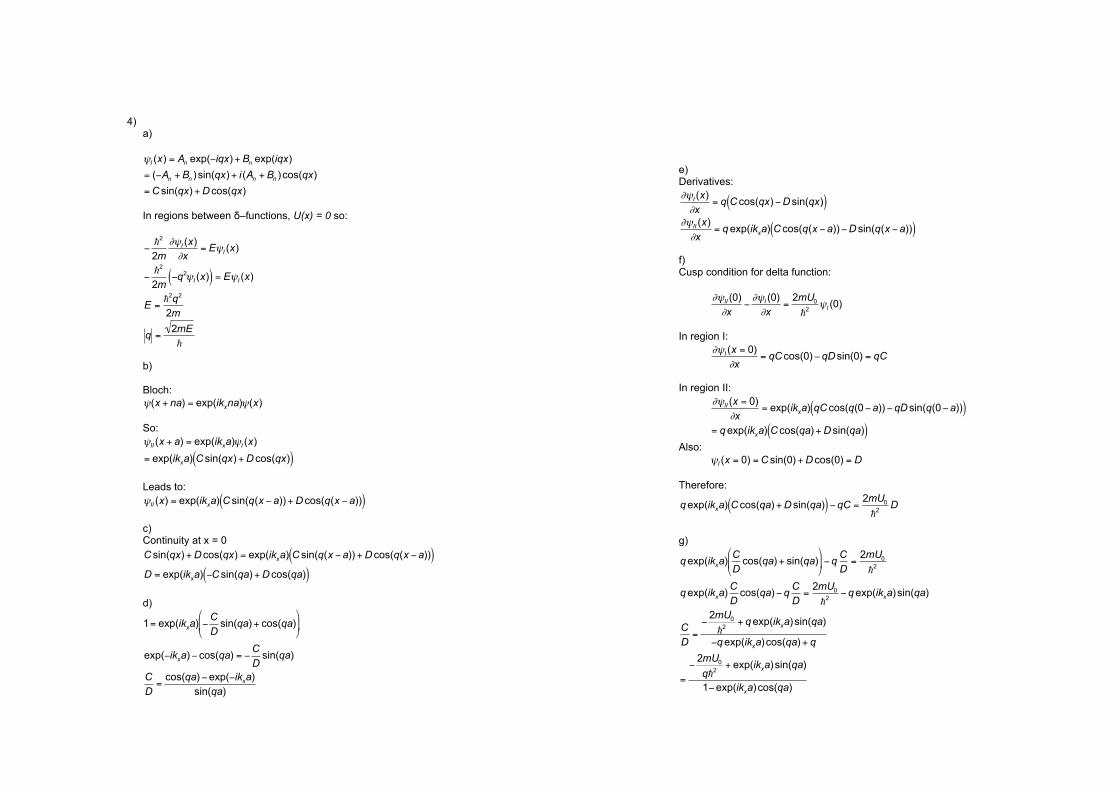
e) Derivatives:
!
"#I (x)"x
= q C cos(qx) $D sin(qx)( )
!
"#II (x)"x
= q exp(ikxa) C cos(q(x $a))$D sin(q(x $a))( ) !
f) Cusp condition for delta function:
!
"#II (0)"x
$"#I (0)"x
=2mU0
!2 #I (0) !!
In region I:
!
"#I (x = 0)"x
= qC cos(0) $qD sin(0) = qC !!In region II:
!
"#II (x = 0)"x
= exp(ikxa) qC cos(q(0$a)) $qD sin(q(0$a))( )= q exp(ikxa) C cos(qa) + D sin(qa)( )
!
Also:
!
"I (x = 0) = C sin(0) + D cos(0) = D ! Therefore:
!
q exp(ikxa) C cos(qa) + D sin(qa)( ) "qC =2mU0
!2D
g)
!
q exp(ikxa) CD
cos(qa) + sin(qa)"
# $
%
& ' (q C
D=
2mU0
!2
q exp(ikxa) CD
cos(qa) (q CD
=2mU0
!2(q exp(ikxa) sin(qa)
CD
=(
2mU0
!2+ q exp(ikxa) sin(qa)
(q exp(ikxa) cos(qa) + q
=(
2mU0
q!2+ exp(ikxa) sin(qa)
1(exp(ikxa) cos(qa)
h)
!
CD
="exp("ikxa) + cos(qa)
sin(qa)="
2mU0
q!2+ exp(ikxa) sin(qa)
1"exp(ikxa) cos(qa)
"exp("ikxa) + cos(qa)( ) 1"exp(ikxa) cos(qa)( )= "
2mU0
q!2sin(qa) + exp(ikxa) sin2(qa)
"exp("ikxa) + cos(qa) + cos(qa) "exp(ikxa) cos2(qa)
= "exp("ikxa) + 2cos(qa) "exp(ikxa) cos2(qa)
= "2mU0
q!2sin(qa) + exp(ikxa) sin2(qa)
"exp("ikxa) + 2cos(qa) "exp(ikxa) cos2(qa) + sin2(qa)( ) = "2mU0
q!2sin(qa)
"exp("ikxa) "exp(ikxa) = "2mU0
q!2sin(qa) "2cos(qa)
"2cos(kxa) = "2mU0
q!2sin(qa) "2cos(qa)
cos(kxa) = cos(qa) +maU0
!2
sin(qa)qa
!
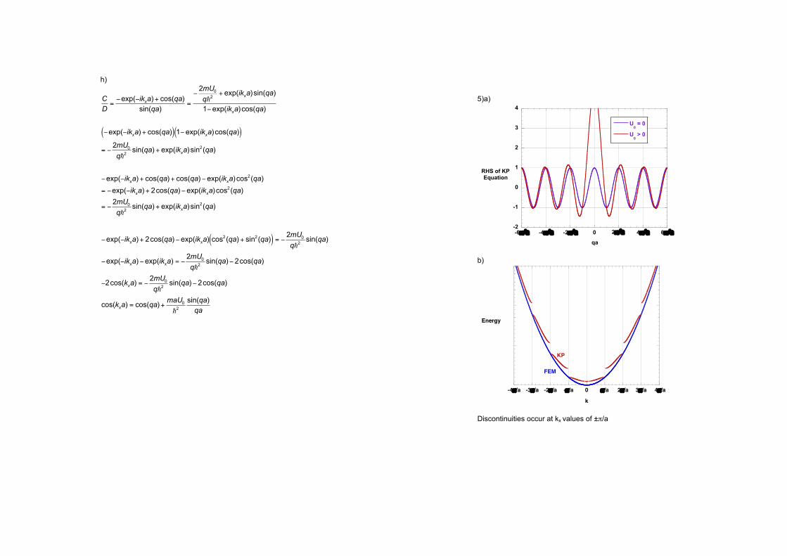
5)a)
b)
Discontinuities occur at kx values of ±!/a
-2
-1
0
1
2
3
4
-6!/a -4!/a -2!/a 0 2!/a 4!/a 6!/a
U0 = 0
U0 > 0
RHS of KPEquation
qa
-4!/a -3!/a -2!/a -!/a 0 !/a 2!/a 3!/a 4!/a
k
Energy
KP
FEM
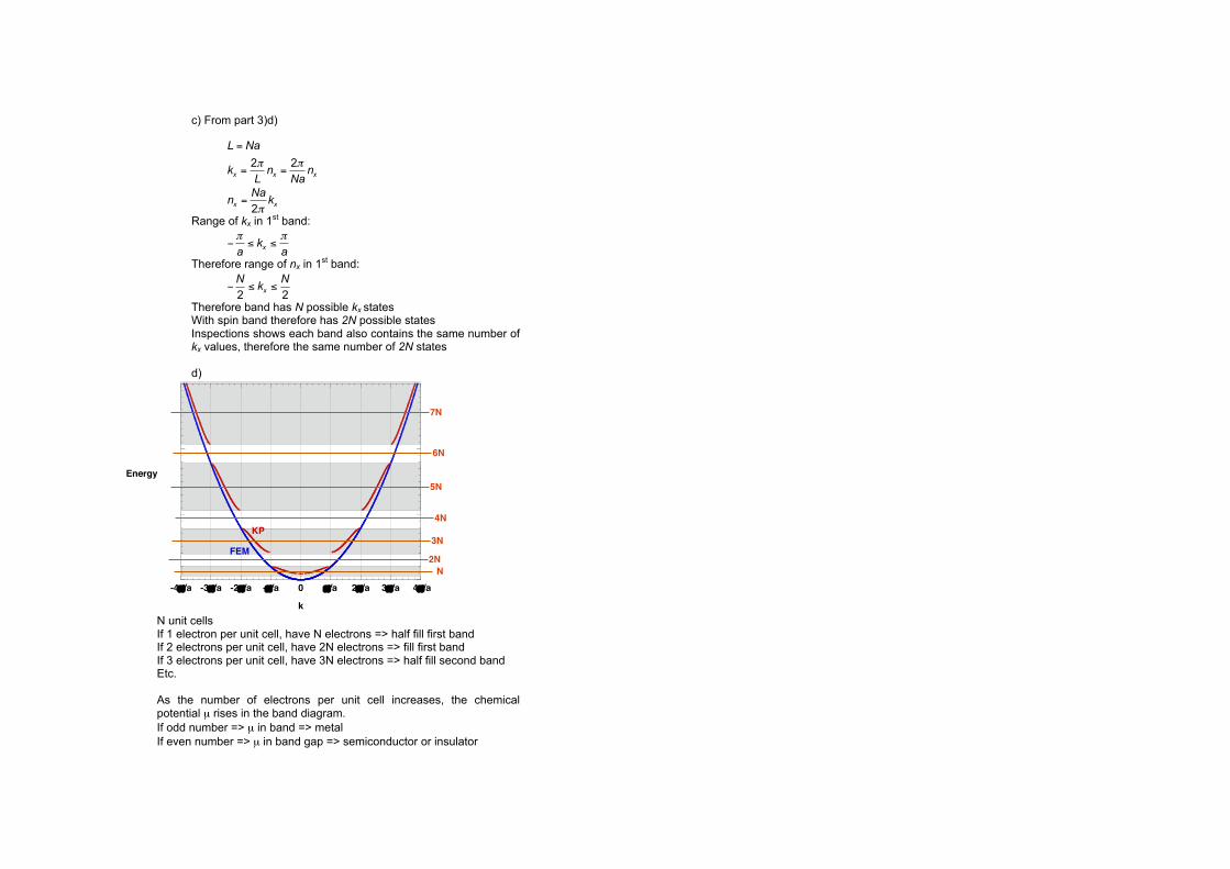
c) From part 3)d)
!
L = Na
kx =2"L
nx =2"Na
nx
!
nx =Na2"
kx
Range of kx in 1st band:
!
"#a$ kx $
#a Therefore range of nx in 1st band:
!
"N2# kx #
N2
Therefore band has N possible kx states With spin band therefore has 2N possible states
Inspections shows each band also contains the same number of kx values, therefore the same number of 2N states
d)
N unit cells If 1 electron per unit cell, have N electrons => half fill first band
If 2 electrons per unit cell, have 2N electrons => fill first band If 3 electrons per unit cell, have 3N electrons => half fill second band Etc. As the number of electrons per unit cell increases, the chemical potential µ rises in the band diagram. If odd number => µ in band => metal If even number => µ in band gap => semiconductor or insulator
-4!/a -3!/a -2!/a -!/a 0 !/a 2!/a 3!/a 4!/a
k
Energy
FEM
KP3N
2N
N
4N
5N
6N
7N
Electrons in Solids (2012)
Problem Sheet 4 SOLUTIONS
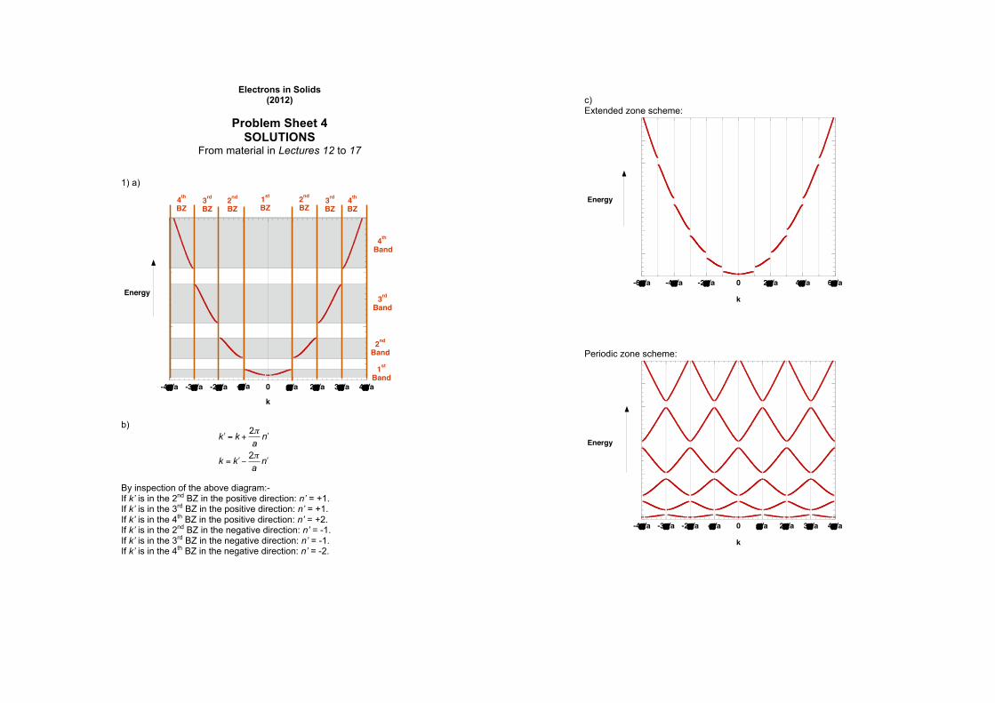
From material in Lectures 12 to 17 1) a)
b) By inspection of the above diagram:- If k’ is in the 2nd BZ in the positive direction: n’ = +1. If k’ is in the 3rd BZ in the positive direction: n’ = +1. If k’ is in the 4th BZ in the positive direction: n’ = +2. If k’ is in the 2nd BZ in the negative direction: n’ = -1. If k’ is in the 3rd BZ in the negative direction: n’ = -1. If k’ is in the 4th BZ in the negative direction: n’ = -2.
-4!/a -3!/a -2!/a -!/a 0 !/a 2!/a 3!/a 4!/a
k
Energy
4th
Band
1st
BZ2
nd
BZ3
rd
BZ4
th
BZ3
rd
BZ
3rd
Band
4th
BZ
2nd
BZ
2nd
Band
1st
Band
!
" k = k +2#
a" n
k = " k $2#
a" n
c) Extended zone scheme:
Periodic zone scheme:
-6!/a -4!/a -2!/a 0 2!/a 4!/a 6!/a
k
Energy
-4!/a -3!/a -2!/a -!/a 0 !/a 2!/a 3!/a 4!/a
k
Energy
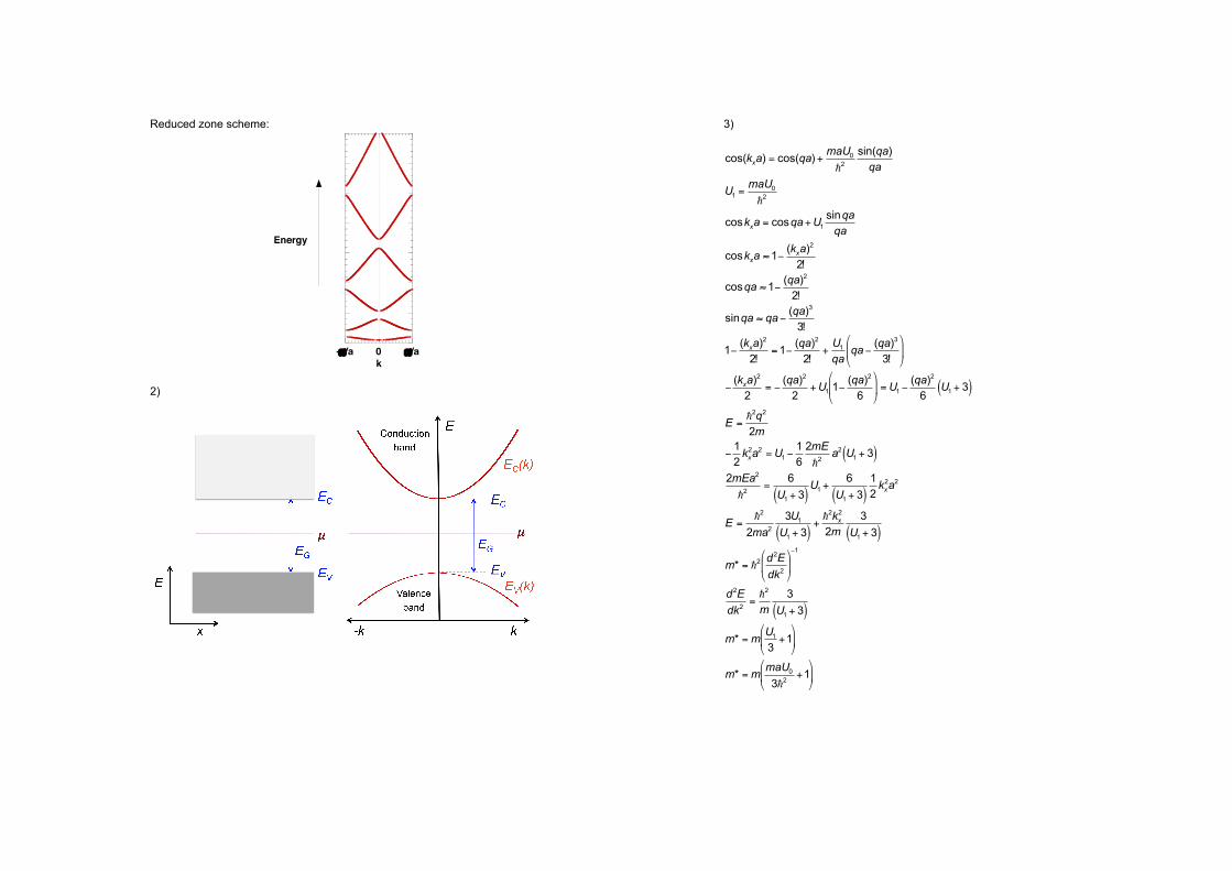
Reduced zone scheme:
2)
-!/a 0 !/a
k
Energy
3)
!
cos(kxa) = cos(qa) +maU0
!2
sin(qa)
qa
U1 =maU0
!2
coskxa = cosqa + U1
sinqa
qa
coskxa "1#(kxa)2
2!
cosqa "1#(qa)2
2!
sinqa " qa#(qa)3
3!
1#(kxa)2
2!= 1#
(qa)2
2!+
U1
qaqa#
(qa)3
3!
$
% &
'
( )
#(kxa)2
2= #
(qa)2
2+ U1 1#
(qa)2
6
$
% &
'
( ) = U1 #
(qa)2
6U1 + 3( )
E =!
2q2
2m
#1
2kx
2a2 = U1 #1
6
2mE
!2
a2 U1 + 3( )
2mEa2
!2
=6
U1 + 3( )U1 +
6
U1 + 3( )1
2kx
2a2
E =!
2
2ma2
3U1
U1 + 3( )+!
2kx
2
2m
3
U1 + 3( )
m* = !2 d2E
dk2
$
% &
'
( )
#1
d2E
dk2=!
2
m
3
U1 + 3( )
m* = mU1
3+1
$
% &
'
( )
m* = mmaU0
3!2+1
$
% &
'
( )
4)
a) 3D FEM DOS
3D FEM E(k) By comparison DOS at conduction band edge: By comparison DOS at conduction band edge: b) The equations which govern the total number of electrons N and holes P in the conduction and valence bands of the semiconductor are:
!
EV(k) = E
V+!
2k
2
2mnV
"
!
EC(k) = E
C+!
2k
2
2mnC
"
!
D(E) =V
2" 2
2m
!2
#
$ %
&
' (
3 / 2
E
!
E =!
2k
2
2m
!
EC(k) "E
C( ) = E "EC( ) =
!2k
2
2mnC
#
DC(E) =
V
2$ 2
2mnC
#
!2
%
&
' '
(
)
* *
3 / 2
E "EC
!
EV(k) "E
V( ) =!
2k
2
2mnV
#= "!
2k
2
2mnV
#
EV"E
V(k)( ) = E
V"E( ) =
!2k
2
2mnV
#
DV(E) =
V
2$ 2
2mnV
#
!2
%
&
' '
(
)
* *
3 / 2
EV"E
!
f (E) =1
exp((E "µ) / kBT ) +1
N = f (E)DC(E)dE
EC
#
$
P = (1" f (E))DV(E)dE
0
EV
$
c) d)
!
N = DC(E)exp("(E "µ) / k
BT )dE
EC
#
$
=V
2% 2
2mnC
&
!2
'
(
) )
*
+
, ,
3 / 2
E "EC( ) exp("(E "µ) / k
BT )dE
EC
#
$
x =E "E
C
kBT
E = kBTx + E
C
dE = kBTdx
LimE-EC
x( ) = 0
LimE-#
x( ) = #
E "EC( ) exp("(E "µ) / k
BT )dE
EC
#
$
= kBTx( ) exp("(k
BTx + E
C"µ) / k
BT )k
BTdx
0
#
$
= kBT( )
3 / 2
exp("(EC"µ) / k
BT ) x exp("x)dx
0
#
$
= kBT( )
3 / 2
exp("(EC"µ) / k
BT )
%
2
N =V
4% 3 / 2
2mnC
&
!2
'
(
) )
*
+
, ,
3 / 2
kBT( )
3 / 2
exp("(EC"µ) / k
BT )
!
1" f (E) = 1"1
exp((E "µ) / kBT ) +1
=exp((E "µ) / k
BT ) +1
exp((E "µ) / kBT ) +1
"1
exp((E "µ) / kBT ) +1
=exp((E "µ) / k
BT )
exp((E "µ) / kBT ) +1
=exp((E "µ) / k
BT )
exp((E "µ) / kBT ) +1
exp("(E "µ) / kBT )
exp("(E "µ) / kBT )
#
$ %
&
' (
=1
exp((µ "E) / kBT ) +1
!
E "µ >> kBT
f (E) =1
exp((E "µ) / kBT ) +1
#1
exp((E "µ) / kBT )
= exp("(E "µ) / kBT )
1" f (E) =1
exp((µ "E) / kBT ) +1
#1
exp((µ "E) / kBT )
= exp("(µ "E) / kBT )
!
P = DV(E)exp("(µ "E) / k
BT )dE
0
EV#
=V
2$ 2
2mnV
%
!2
&
'
( (
)
*
+ +
3 / 2
EV"E( ) exp("(µ "E) / k
BT )dE
0
EV#
x =E
V"E
kBT
E = "kBTx + E
V
dE = "kBTdx
LimE,EV
x( ) = 0
LimE,0
x( ) =E
V
kBT
>> 1
-LimE,0
x( ) . /
EV"E( ) exp("(µ "E) / k
BT )dE
0
EV#
= " kBTx( ) exp("(µ + k
BTx "E
V) / k
BT )k
BTdx
/
0
#
= " kBT( )
3 / 2
exp("(µ "EV) / k
BT ) x exp("x)dx
/
0
#
= kBT( )
3 / 2
exp("(µ "EV) / k
BT )
$
2
P =V
4$ 3 / 2
2mnV
%
!2
&
'
( (
)
*
+ +
3 / 2
kBT( )
3 / 2
exp("(µ "EV) / k
BT )
!
mn
" = mnC
"
n =N
V
n =1
4
2mn
"k
BT
#!2
$
% &
'
( )
3 / 2
exp(*(EC*µ) / k
BT )
n = NC
exp(*(EC*µ) / k
BT )
NC
= 2m
n
"k
BT
2#!2
$
% &
'
( )
3 / 2
!
mp
" = mnv
"
p =P
V
p =1
4
2mp
"kBT
#!2
$
% & &
'
( ) )
3 / 2
exp(*(µ *EV ) / kBT )
p = NV exp(*(µ *EV ) / kBT )
NV = 2mp
"kBT
2#!2
$
% & &
'
( ) )
3 / 2
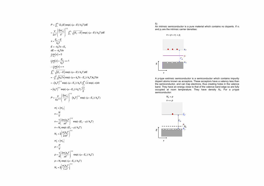
5) An intrinsic semiconductor is a pure material which contains no dopants. If ni and pi are the intrinsic carrier densities:
A p-type extrinsic semiconductor is a semiconductor which contains impurity dopant atoms known as acceptors. These acceptors have a valency less than the semiconductor, and can trap electrons, thus creating holes in the valence band. They have an energy close to that of the valence band edge so are fully occupied at room temperature. They have density NA. For a p-type semiconductor:
!
n = p = ni = pi
!
NA " p
n << p
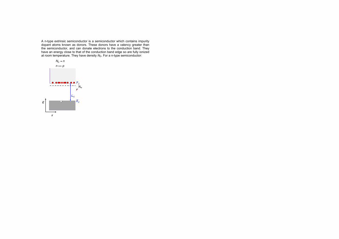
A n-type extrinsic semiconductor is a semiconductor which contains impurity dopant atoms known as donors. These donors have a valency greater than the semiconductor, and can donate electrons to the conduction band. They have an energy close to that of the conduction band edge so are fully ionized at room temperature. They have density ND. For a n-type semiconductor:
!
ND " n
n >> p


![Mia. appearance [ə'p ɪ ərəns] Can you find some differences between us?](https://static.fdocument.org/doc/165x107/56649de45503460f94adb1c9/mia-appearance-p-rns-can-you-find-some-differences-between-us.jpg)
![Ω−Ω =Ω - UPTshannon.etc.upt.ro/teaching/sp-pi/Seminar/2_transf_z_en.pdf3 a) Write the finite difference equation b) Find the impulse response h[n] c) Find the transfer function](https://static.fdocument.org/doc/165x107/5afc7a4b7f8b9aa34d8c22c9/-a-write-the-finite-difference-equation-b-find-the-impulse-response.jpg)