Practical Considerations in the Design of Thermoelectric ...
et38b-2.ppt 1
Practical Sample and Hold Circuit
Control input open and closes solid-state switch at sampling rate
fs .
Modes of operation - tracking ( switch closed) hold (switch open)
Sample and Hold Parameters
acquisition time - time for instant switch closes until Vi within
defined % of input. Determined by input time constant
τ = RinC 5τ value = 99.3% of final value
aperture time - time it takes switch to open
decay rate - rate of discharge of C when circuit is in hold mode

et38b-2.ppt 2
Sampling Rate
To accurately reproduce the analog input data with
samples the sampling rate, fs, must be twice as high
as the highest frequency expected in the input signal.
This is known as the Nyquist criterion.
fs(min) = 2fh
Where fh = the highest discernible f component
in input signal
fs(min) = minimum sampling f
Nyquist rate is the minimum frequency and requires
an ideal pulse to reconstruct the original signal into
an analog value
Sampling a signal is a form of modulation that creates
signals that have a fundmental frequency spectrum
of the original signal and an infinite number of
harmonic aliases.
et38b-2.ppt 3
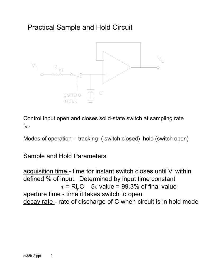
Sampled Signal Frequency Spectrum
frequency
V
fhfs 2fs
fs+fhfs-fh 2fs+fh2fs-fh
Sampling above occurs with fs >2fh
Sampling at less than 2fh causes aliasing and folding of
sampled signals. This means that the original information
will not be reproduced at the same frequency as the original
Folding occurs when the lower frequencies of a harmonic
envelope coincide with the higher frequencies of another
envelope.
fh fs 2fs
fs+fh
fs-fh 2fs+fh
2fs-fh
et38b-2.ppt 4
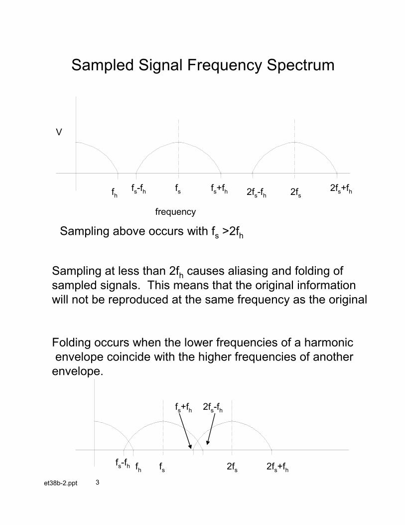
Aliasing occurs when a harmonic frequency is
introduced into the original input frequency range.
For signals to be reconstructed correctly, the harmonic
components must all occur in the range 0 to fs/2.
Take a frequency spectrum view of the sampled signals
to get a better understanding of the aliasing and folding.
Sampling at fs = 1000 Hz with an input frequency of
fin of 100 Hz. Ten samples/period- above Nyquist
rate
Lowpass filter extracts the range 0 to 500 Hz
0 to +fs/2
Lower fs : let fs = 60 Hz
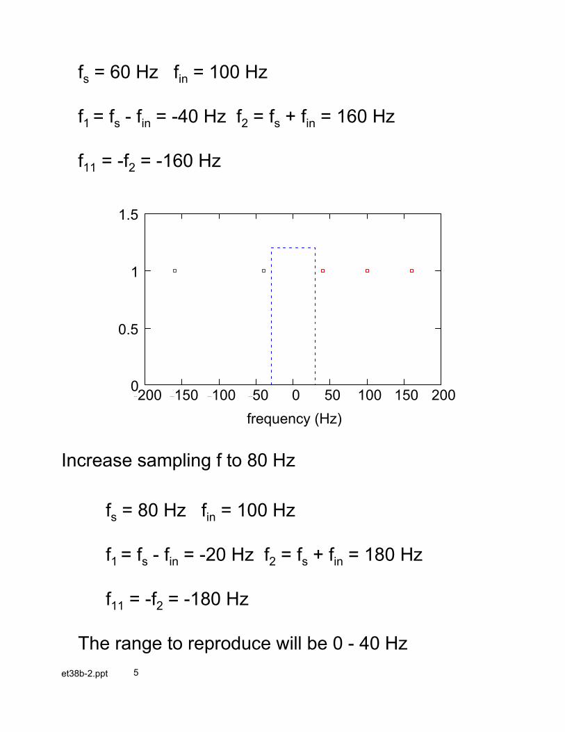
et38b-2.ppt 5
fs = 60 Hz fin = 100 Hz
f1 = fs - fin = -40 Hz f2 = fs + fin = 160 Hz
f11 = -f2 = -160 Hz
Increase sampling f to 80 Hz
fs = 80 Hz fin = 100 Hz
f1 = fs - fin = -20 Hz f2 = fs + fin = 180 Hz
f11 = -f2 = -180 Hz
The range to reproduce will be 0 - 40 Hz
200 150 100 50 0 50 100 150 2000
0.5
1
1.5
frequency (Hz)
et38b-2.ppt 6
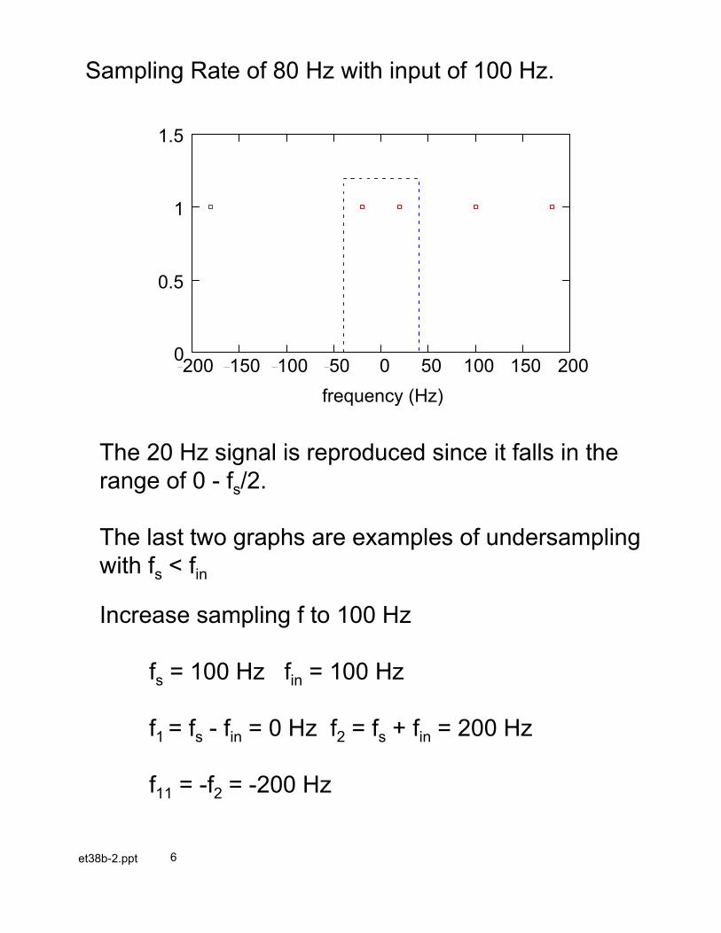
Sampling Rate of 80 Hz with input of 100 Hz.
The 20 Hz signal is reproduced since it falls in the
range of 0 - fs/2.
The last two graphs are examples of undersampling
with fs < fin
Increase sampling f to 100 Hz
fs = 100 Hz fin = 100 Hz
f1 = fs - fin = 0 Hz f2 = fs + fin = 200 Hz
f11 = -f2 = -200 Hz
200 150 100 50 0 50 100 150 2000
0.5
1
1.5
frequency (Hz)
et38b-2.ppt 7
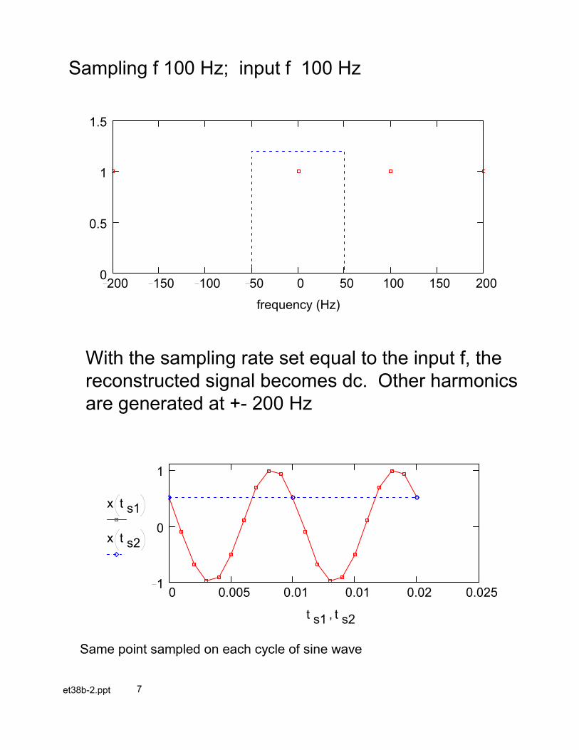
Sampling f 100 Hz; input f 100 Hz
With the sampling rate set equal to the input f, the
reconstructed signal becomes dc. Other harmonics
are generated at +- 200 Hz
Same point sampled on each cycle of sine wave
200 150 100 50 0 50 100 150 2000
0.5
1
1.5
frequency (Hz)
0 0.005 0.01 0.01 0.02 0.0251
0
1
x t s1
x t s2
,t s1 t s2

et38b-2.ppt 8
Folding occurs when fs > fin bus less than the
Nyquist Rate.
fs = 125 Hz fin = 100 Hz
f1 = fs - fin = 25 Hz f2 = fs + fin = 225 Hz
f11 = -f2 = -225 Hz
A 25 Hz signal is reconstructed since it falls in the
range 0 to fs/2.
With a sample rate of 125 Hz we get the same
points as though we had sampled a 25 Hz signal
The lower frequencies of fs appear in range 0- 62.5 Hz
250 200 150 100 50 0 50 100 150 200 2500
0.5
1
1.5
frequency (Hz)
et38b-2.ppt 9
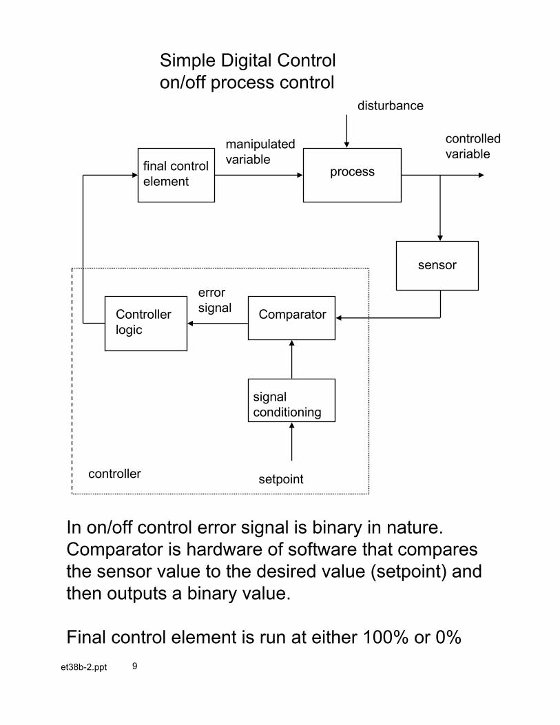
Simple Digital Control
on/off process control
process
disturbance
sensor
final control
element
controlled
variablemanipulated
variable
Comparator
signal
conditioning
Controller
logic
error
signal
setpointcontroller
In on/off control error signal is binary in nature.
Comparator is hardware of software that compares
the sensor value to the desired value (setpoint) and
then outputs a binary value.
Final control element is run at either 100% or 0%
et38b-2.ppt 10
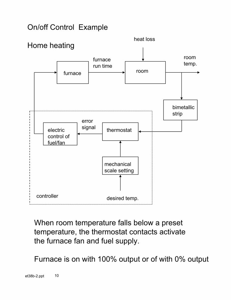
On/off Control Example
Home heating
room
bimetallic
strip
furnace
room
temp.furnace
run time
thermostat
mechanical
scale setting
electric
control of
fuel/fan
error
signal
desired temp.controller
heat loss
When room temperature falls below a preset
temperature, the thermostat contacts activate
the furnace fan and fuel supply.
Furnace is on with 100% output or of with 0% output
et38b-2.ppt 11
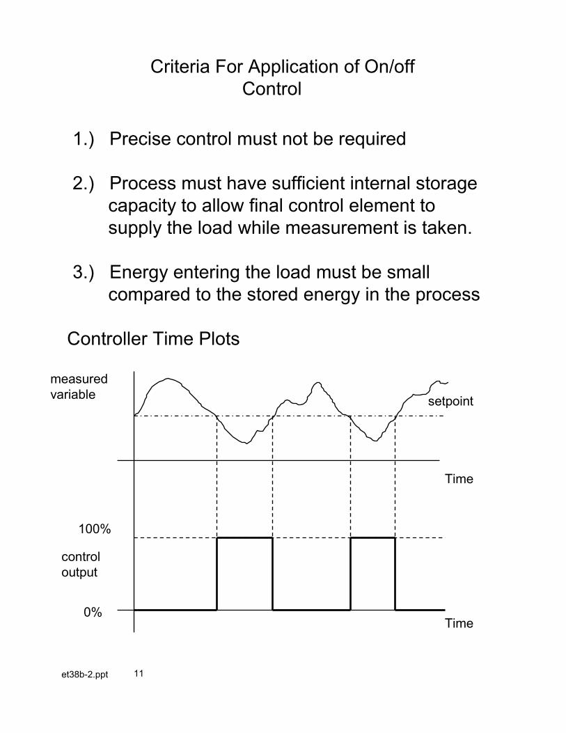
Criteria For Application of On/off
Control
1.) Precise control must not be required
2.) Process must have sufficient internal storage
capacity to allow final control element to
supply the load while measurement is taken.
3.) Energy entering the load must be small
compared to the stored energy in the process
Controller Time Plots
Time
Time
control
output
0%
100%
measured
variablesetpoint
et38b-2.ppt 12
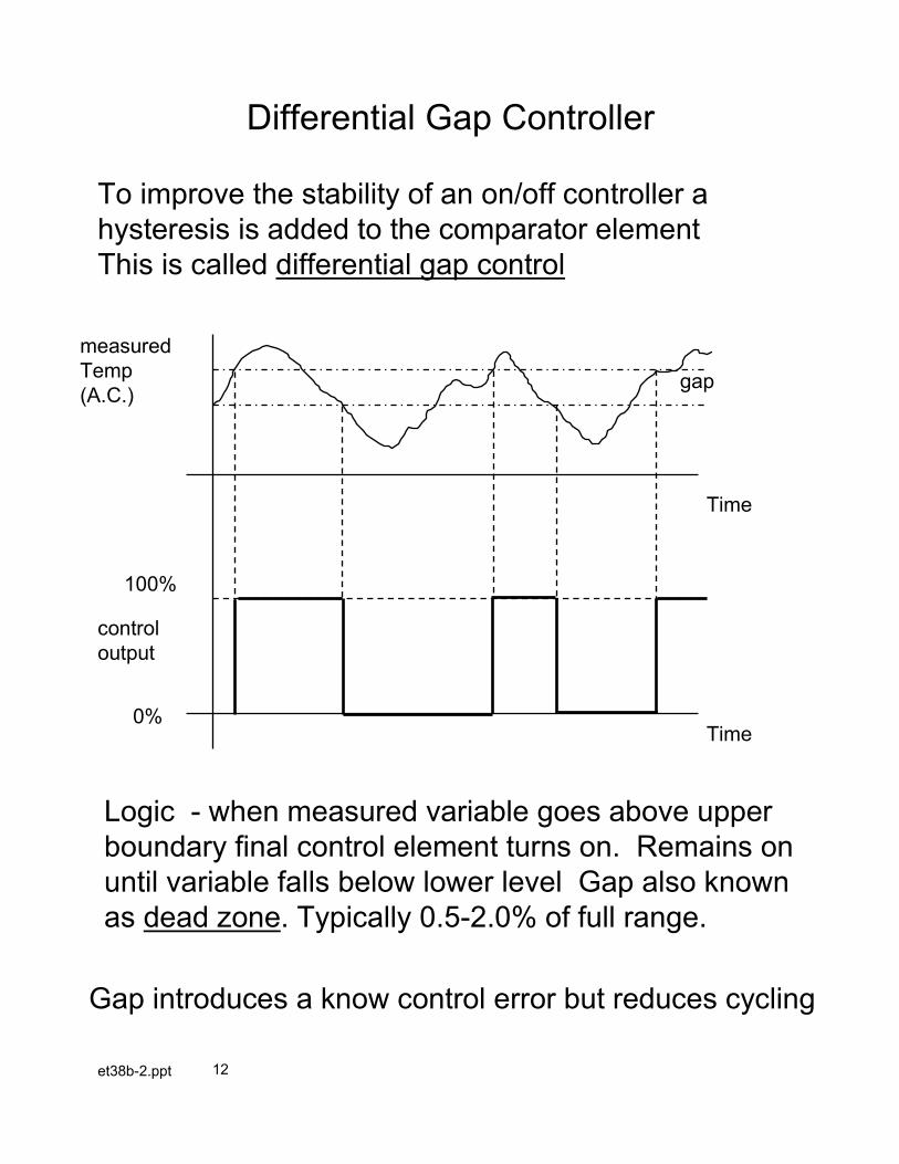
Differential Gap Controller
To improve the stability of an on/off controller a
hysteresis is added to the comparator element
This is called differential gap control
Time
Time
control
output
0%
100%
measured
Temp
(A.C.)gap
Logic - when measured variable goes above upper
boundary final control element turns on. Remains on
until variable falls below lower level Gap also known
as dead zone. Typically 0.5-2.0% of full range.
Gap introduces a know control error but reduces cycling
et38b-2.ppt 13
Analog Signal Conversion
Number of bits in digital signal determines the
resolution of the digital signals.
Depends on voltage span also.
Two Problems
Input - analog-to-digital conversion
continuous signals converted to
discrete values (Analog -to-digital)
Output - digital-to-analog conversion
discrete values converted to
continuous signals
(Digital-to-analog)
Resolution - smallest number that can be
measured
Accuracy - is the number measured correct
et38b-2.ppt 14
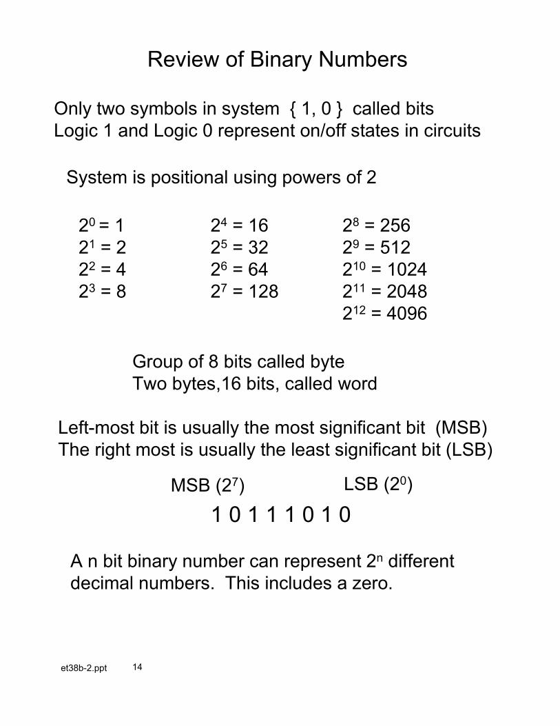
Review of Binary Numbers
Only two symbols in system 1, 0 called bits
Logic 1 and Logic 0 represent on/off states in circuits
System is positional using powers of 2
20 = 1 24 = 16 28 = 256
21 = 2 25 = 32 29 = 512
22 = 4 26 = 64 210 = 1024
23 = 8 27 = 128 211 = 2048
212 = 4096
1 0 1 1 1 0 1 0
Group of 8 bits called byte
Two bytes,16 bits, called word
Left-most bit is usually the most significant bit (MSB)
The right most is usually the least significant bit (LSB)
MSB (27) LSB (20)
A n bit binary number can represent 2n different
decimal numbers. This includes a zero.
et38b-2.ppt 15
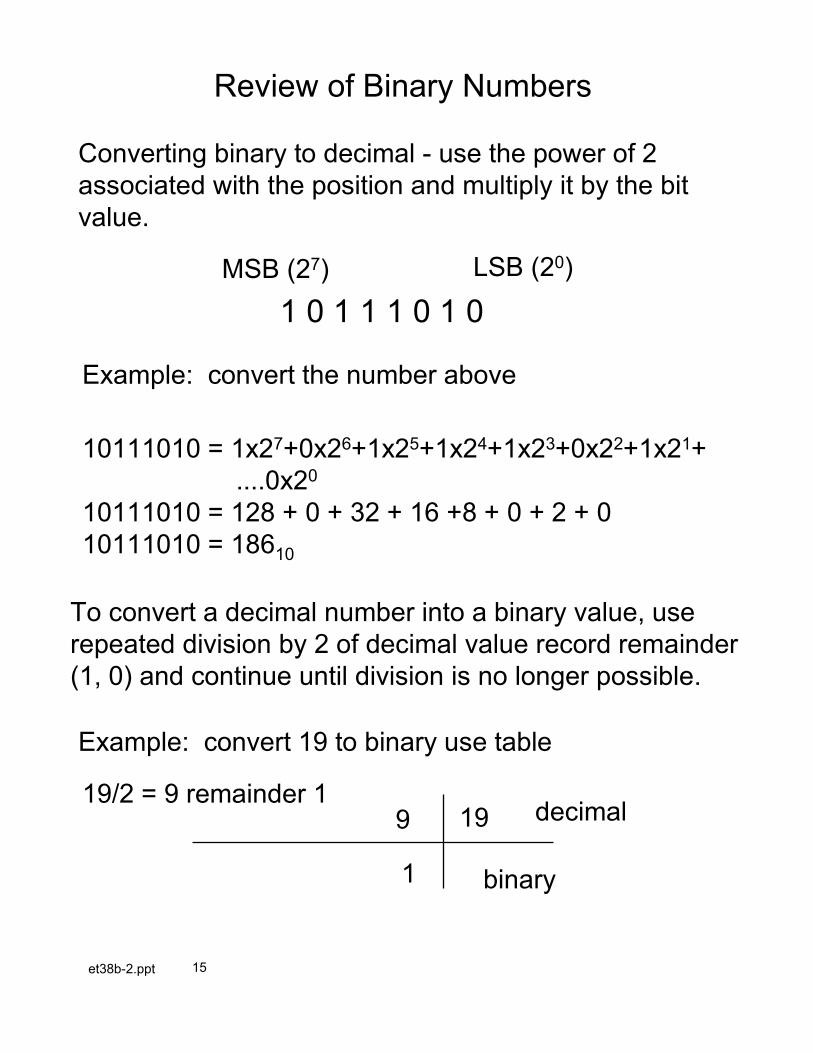
Review of Binary Numbers
Converting binary to decimal - use the power of 2
associated with the position and multiply it by the bit
value.
1 0 1 1 1 0 1 0
MSB (27) LSB (20)
Example: convert the number above
10111010 = 1x27+0x26+1x25+1x24+1x23+0x22+1x21+
....0x20
10111010 = 128 + 0 + 32 + 16 +8 + 0 + 2 + 0
10111010 = 18610
To convert a decimal number into a binary value, use
repeated division by 2 of decimal value record remainder
(1, 0) and continue until division is no longer possible.
Example: convert 19 to binary use table
decimal
binary
1919/2 = 9 remainder 1
9
1
et38b-2.ppt 16
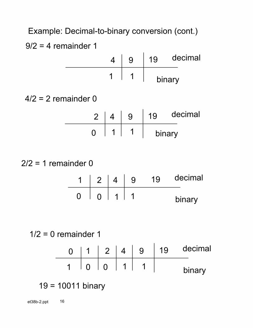
Example: Decimal-to-binary conversion (cont.)
decimal
binary
19
9/2 = 4 remainder 1
9
11
4
decimal
binary
19
4/2 = 2 remainder 0
9
11
4
0
2
decimal
binary
199
11
4
0
2
2/2 = 1 remainder 0
0
1
decimal
binary
199
11
4
0
2
1/2 = 0 remainder 1
0
1
1
0
19 = 10011 binary
et38b-2.ppt 17
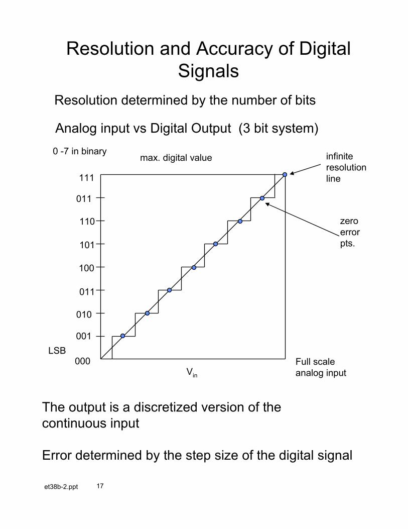
Resolution and Accuracy of Digital
Signals
Analog input vs Digital Output (3 bit system)
0 -7 in binary
The output is a discretized version of the
continuous input
Error determined by the step size of the digital signal
Resolution determined by the number of bits
000
001
010
011
100
101
110
011
111
max. digital value
Full scale
analog inputVin
zero
error
pts.
infinite
resolution
line
LSB
et38b-2.ppt 18
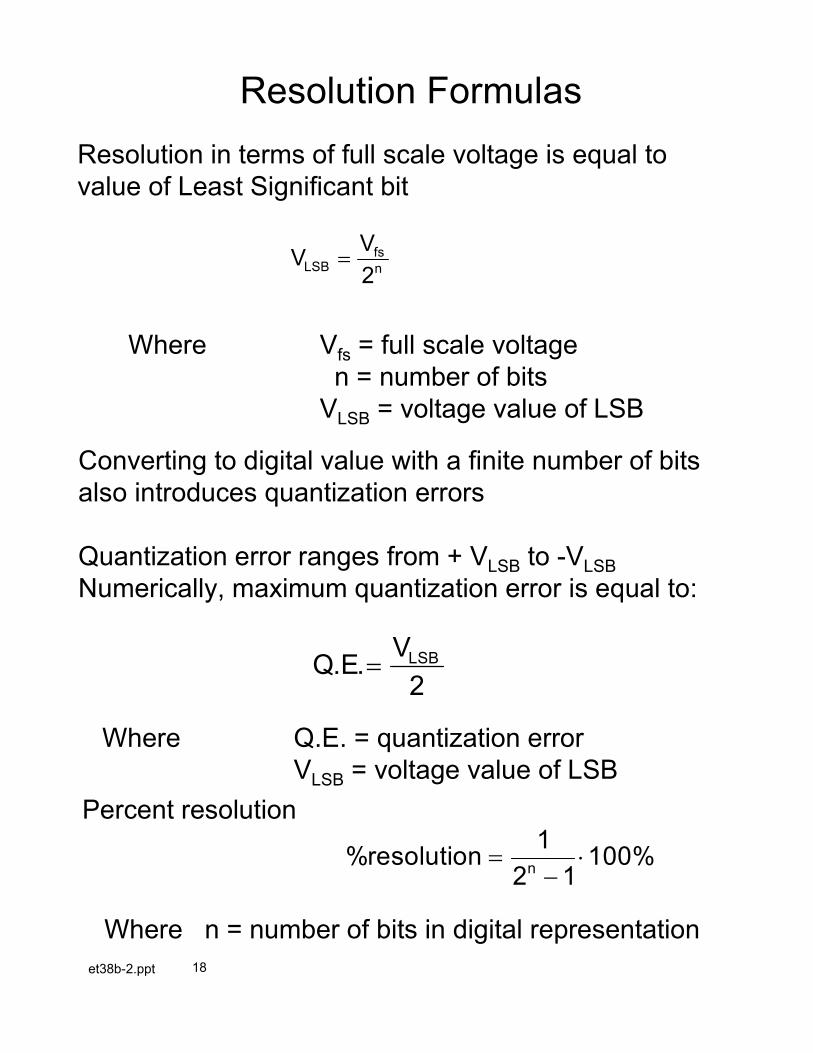
Percent resolution
%resolutionn
=−
⋅1
2 1100%
Where n = number of bits in digital representation
Where Vfs = full scale voltage
n = number of bits
VLSB = voltage value of LSB
Resolution in terms of full scale voltage is equal to
value of Least Significant bit
Resolution Formulas
Converting to digital value with a finite number of bits
also introduces quantization errors
Quantization error ranges from + VLSB to -VLSB
Numerically, maximum quantization error is equal to:
Q EVLSB. .=2
VV
LSBfs
n=
2
Where Q.E. = quantization error
VLSB = voltage value of LSB
et38b-2.ppt 19
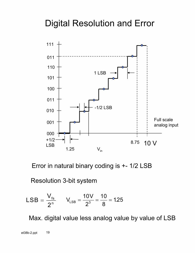
Digital Resolution and Error
000
001
010
011
100
101
110
011
111
Full scale
analog input
Vin
1 LSB
+1/2
LSB
-1/2 LSB
Error in natural binary coding is +- 1/2 LSB
10 V
Resolution 3-bit system
LSBVfs
n=
2V
VLSB = = =
10
2
10
8125
3.
Max. digital value less analog value by value of LSB
1.25
8.75
et38b-2.ppt 20
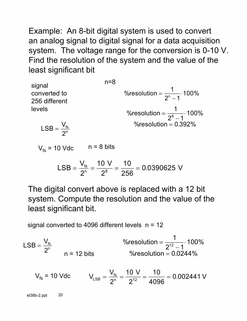
Example: An 8-bit digital system is used to convert
an analog signal to digital signal for a data acquisition
system. The voltage range for the conversion is 0-10 V.
Find the resolution of the system and the value of the
least significant bit
The digital convert above is replaced with a 12 bit
system. Compute the resolution and the value of the
least significant bit.
n=8
%resolutionn
=−
⋅1
2 1100%
LSBVfs
n=
2
Vfs = 10 Vdc n = 8 bits
%
% .
resolution
resolution
=−
⋅
=
1
2 1100%
0 392%
8
signal
converted to
256 different
levels
LSBVfs
n=
2
Vfs = 10 Vdc
n = 12 bits
signal converted to 4096 different levels n = 12
%
% .
resolution
resolution
=−
⋅
=
1
2 1100%
0 0244%
12
LSBVfs
n= = = =
2
10
2
10
2560 0390625
8
V V.
VV
LSBfs
n= = = =
2
10
2
10
40960 002441
12
V V.
et38b-2.ppt 21
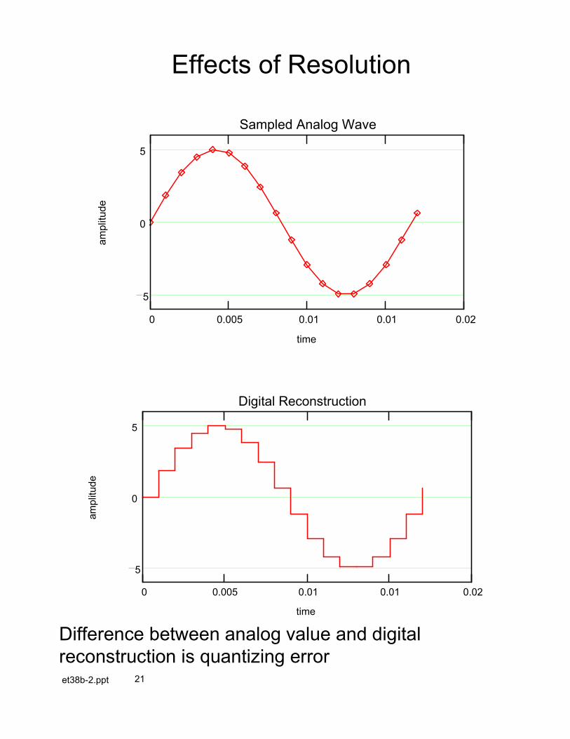
Effects of Resolution
0 0.005 0.01 0.01 0.02
5
0
5
Sampled Analog Wave
time
amplitude
0 0.005 0.01 0.01 0.02
5
0
5
Digital Reconstruction
time
amplitude
Difference between analog value and digital
reconstruction is quantizing error
et38b-2.ppt 22
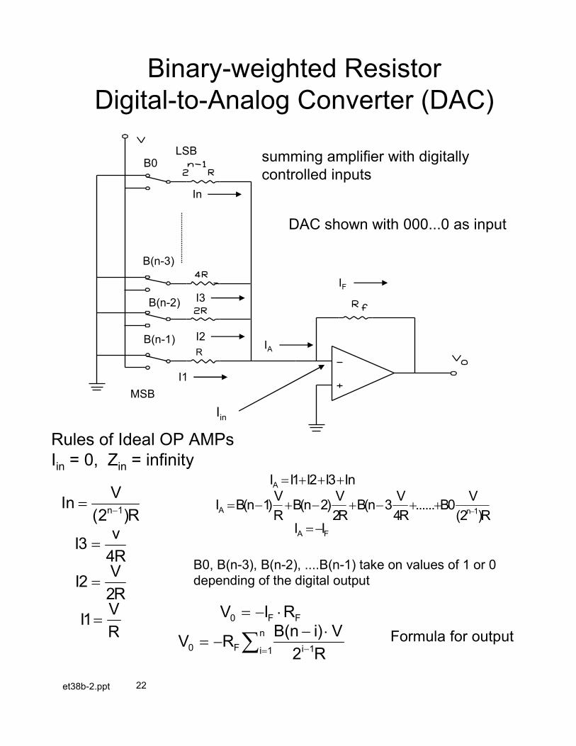
Binary-weighted Resistor
Digital-to-Analog Converter (DAC)
summing amplifier with digitally
controlled inputs
DAC shown with 000...0 as input
In
I3
I2
I1
Rules of Ideal OP AMPs
Iin = 0, Zin = infinity
Iin
IA
IF
B0
B(n-3)
B(n-2)
B(n-1)
B0, B(n-3), B(n-2), ....B(n-1) take on values of 1 or 0
depending of the digital output
Formula for output
R
InV
R
Iv
R
IV
R
IV
R
n=
=
=
=
−( )2
34
22
1
1
I I I I In
I BV
RB
V
RB
V
RI I
BV
R
A
A
A F
n
= + + +
= − + − + −
= −
+ +−
1 2 3
1 22
34
02 1
(n ) (n ) (n ......( )
MSB
LSB
V I R
V RB i V
R
F F
F ii
n
0
0 11 2
= − ⋅
= −− ⋅−=∑
(n )
et38b-2.ppt 23
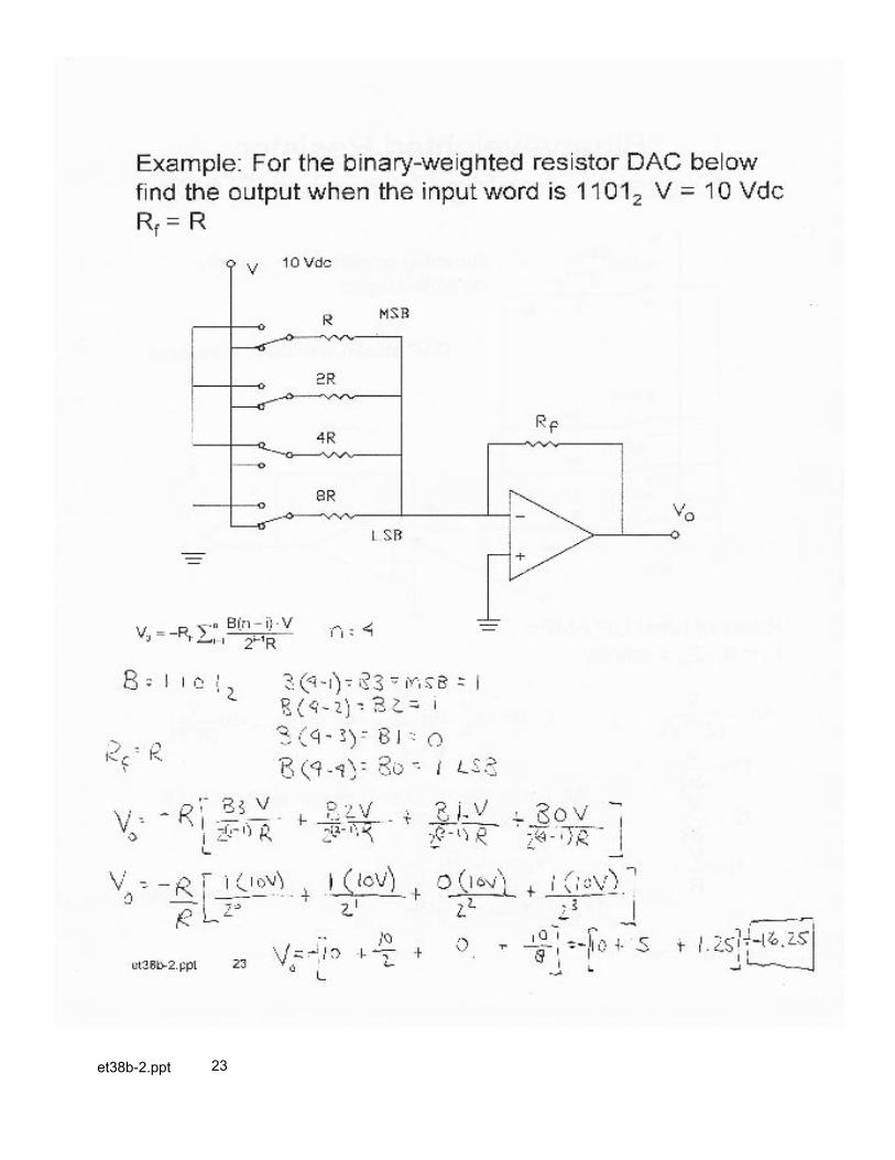
Example: For the binary-weighted resistor DAC below
find the output when the input word is 11012 V = 10 Vdc
Rf = R
10 Vdc
V RB i V
RF ii
n
0 11 2= −
− ⋅−=∑
(n )
et38b-2.ppt 24
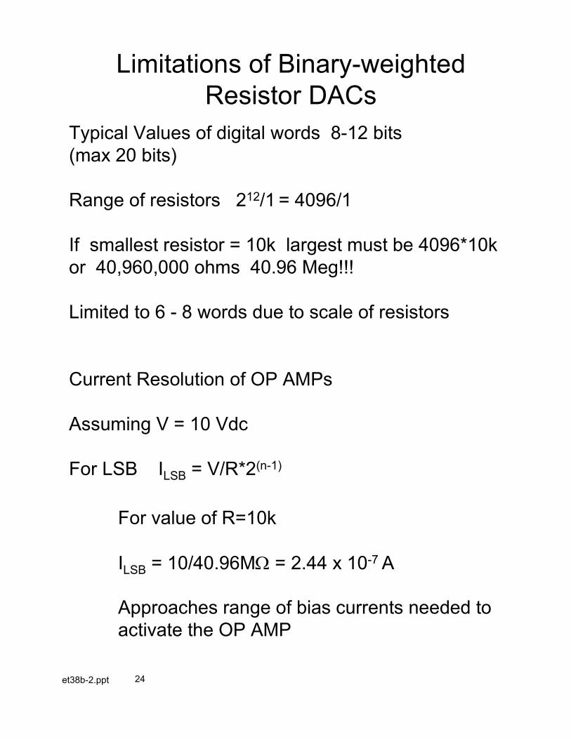
Limitations of Binary-weighted
Resistor DACs
Typical Values of digital words 8-12 bits
(max 20 bits)
Range of resistors 212/1 = 4096/1
If smallest resistor = 10k largest must be 4096*10k
or 40,960,000 ohms 40.96 Meg!!!
Limited to 6 - 8 words due to scale of resistors
Current Resolution of OP AMPs
Assuming V = 10 Vdc
For LSB ILSB = V/R*2(n-1)
For value of R=10k
ILSB = 10/40.96MΩ = 2.44 x 10⁻⁷ A
Approaches range of bias currents needed to
activate the OP AMP


![Manchester Practical [وضع التوافق]](https://static.fdocument.org/doc/165x107/556e0fb4d8b42aba5d8b5162/manchester-practical-.jpg)