PPE Basic Topologies - USPAS | U.S. Particle...
103
Pulsed Power Engineering Basic Topologies January 12-16, 2009 Craig Burkhart, PhD Power Conversion Department SLAC National Accelerator Laboratory
Transcript of PPE Basic Topologies - USPAS | U.S. Particle...
Pulsed Power EngineeringBasic Topologies
January 12-16, 2009
Craig Burkhart, PhDPower Conversion Department
SLAC National Accelerator Laboratory
January 12-16, 2009 USPAS Pulsed Power Engineering C Burkhart 2
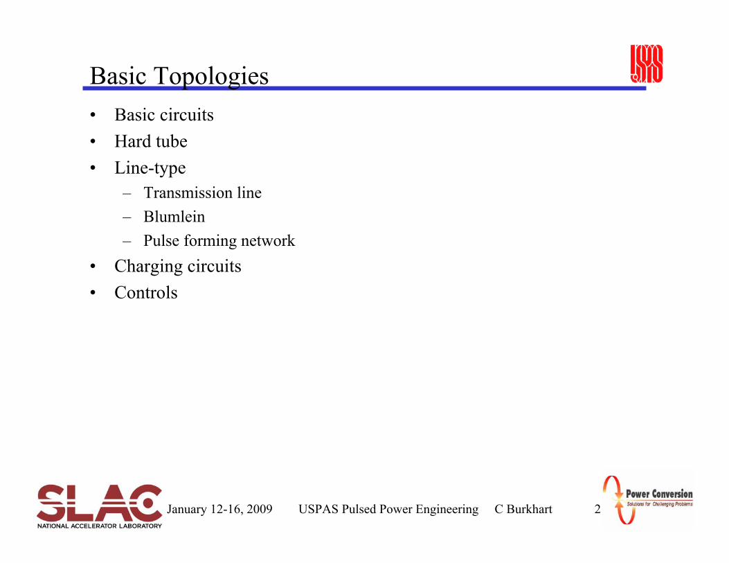
Basic Topologies• Basic circuits• Hard tube• Line-type
– Transmission line– Blumlein– Pulse forming network
• Charging circuits• Controls
January 12-16, 2009 USPAS Pulsed Power Engineering C Burkhart 3
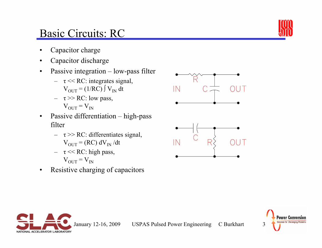
Basic Circuits: RC• Capacitor charge• Capacitor discharge• Passive integration – low-pass filter
– τ << RC: integrates signal, VOUT = (1/RC) ∫ VIN dt
– τ >> RC: low pass, VOUT = VIN
• Passive differentiation – high-pass filter
– τ >> RC: differentiates signal, VOUT = (RC) dVIN /dt
– τ << RC: high pass, VOUT = VIN
• Resistive charging of capacitors
January 12-16, 2009 USPAS Pulsed Power Engineering TTU-PPSC 4
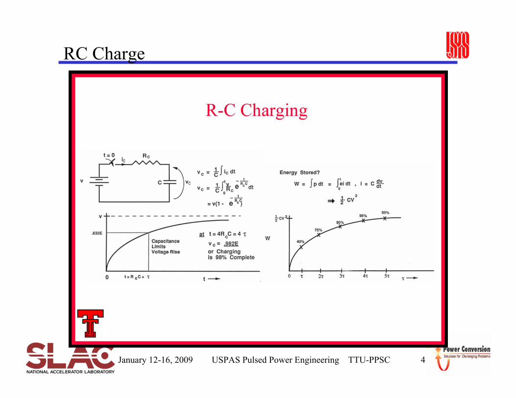
RC Charge
January 12-16, 2009 USPAS Pulsed Power Engineering TTU-PPSC 5
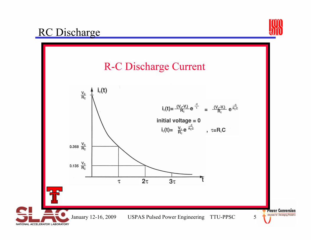
RC Discharge
January 12-16, 2009 USPAS Pulsed Power Engineering TTU/Burkhart 6
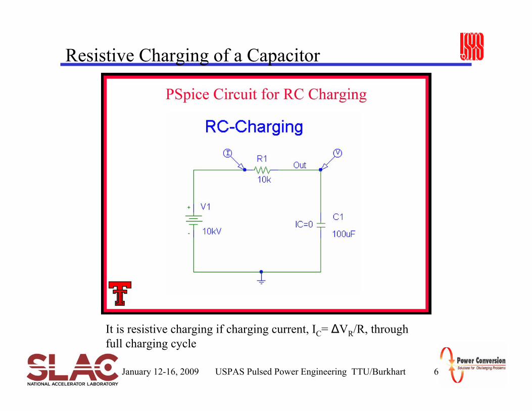
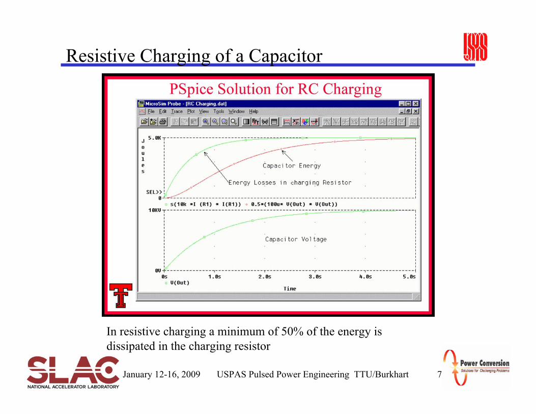
Resistive Charging of a Capacitor
It is resistive charging if charging current, IC= ΔVR/R, through full charging cycle
January 12-16, 2009 USPAS Pulsed Power Engineering TTU/Burkhart 7
Resistive Charging of a Capacitor
In resistive charging a minimum of 50% of the energy is dissipated in the charging resistor
January 12-16, 2009 USPAS Pulsed Power Engineering C Burkhart 8
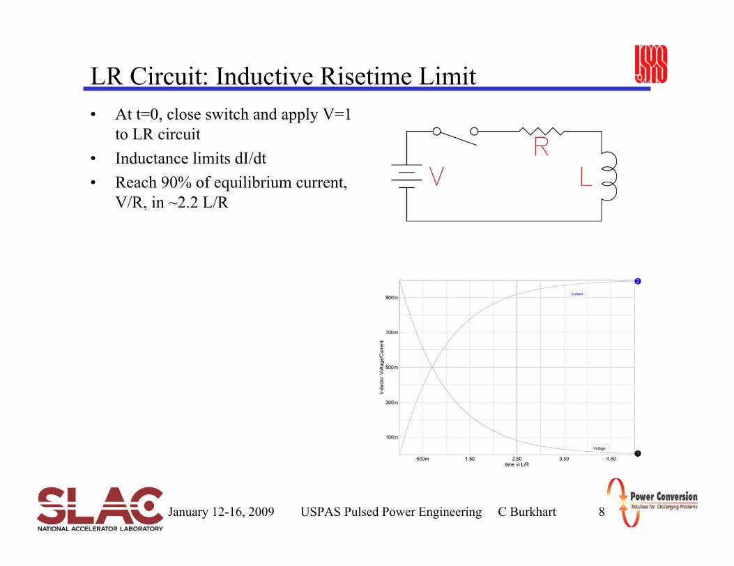
LR Circuit: Inductive Risetime Limit• At t=0, close switch and apply V=1
to LR circuit• Inductance limits dI/dt• Reach 90% of equilibrium current,
V/R, in ~2.2 L/R
January 12-16, 2009 USPAS Pulsed Power Engineering C Burkhart 9
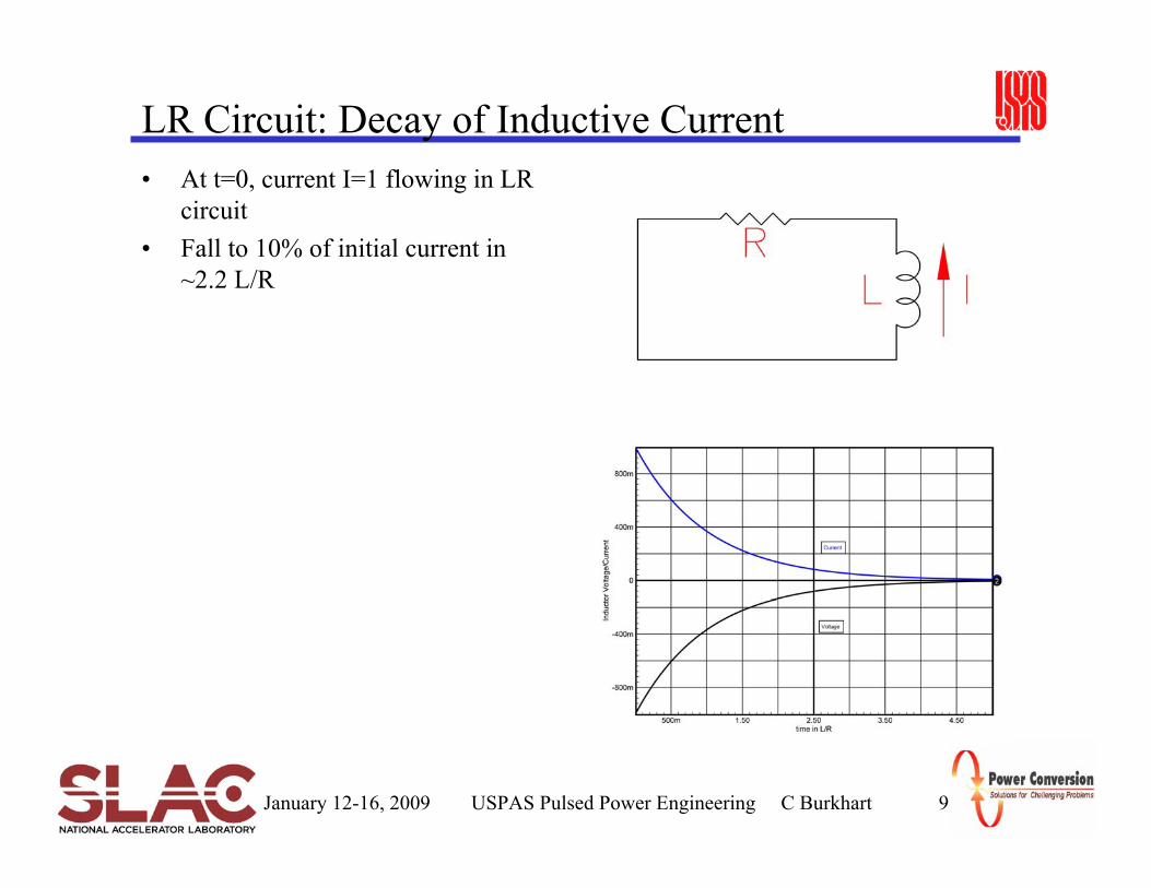
LR Circuit: Decay of Inductive Current• At t=0, current I=1 flowing in LR
circuit• Fall to 10% of initial current in
~2.2 L/R
January 12-16, 2009 USPAS Pulsed Power Engineering C Burkhart 10
LRC Circuit• Generally applicable to a wide number of circuits and sub-circuits
found in pulsed power systems• Presented in the more general form of CLRC (after NSRC formulary)
– Limit C1 → ∞, reduces to familiar LRC with power supply– Limit C2 → ∞ (short), reduces to familiar LRC– Limit R → 0, reduces to ideal CLC energy transfer– Limit L → 0, reduces to RC
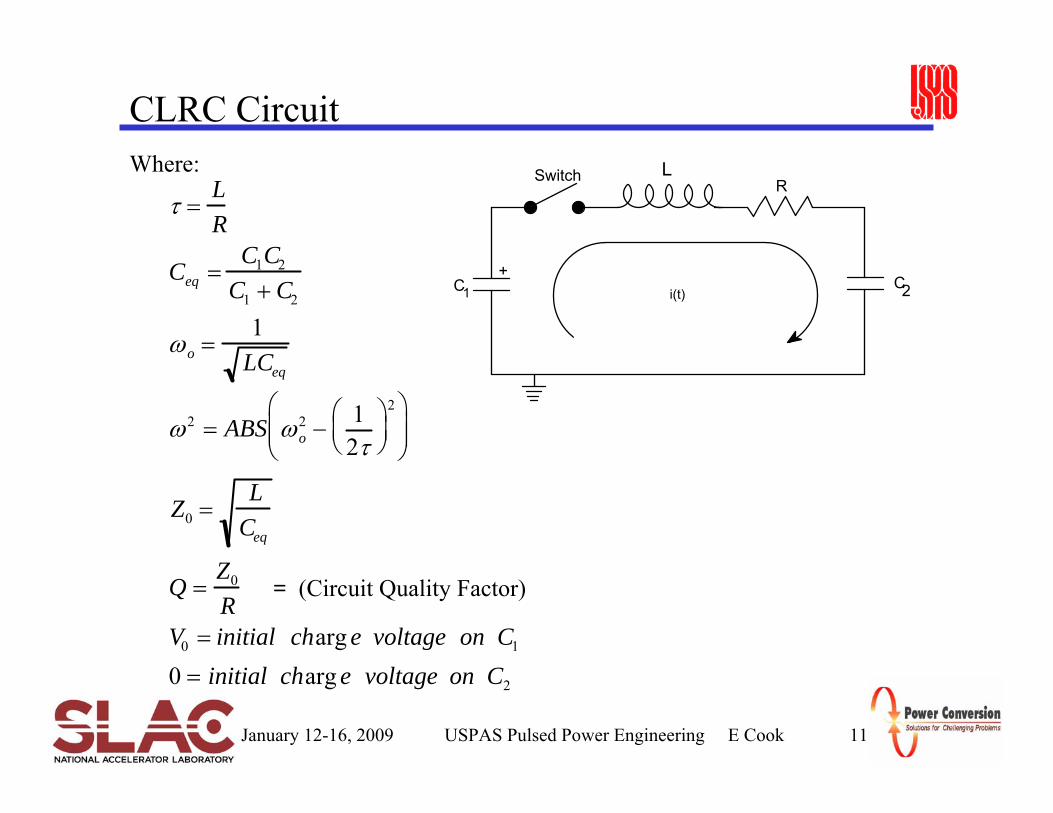
January 12-16, 2009 USPAS Pulsed Power Engineering E Cook 11
CLRC Circuit
+C1
LR
C2
Switch
i(t)
τ =LR
Ceq =C1C2
C1 + C2
ωo =1
LCeq
ω2 = ABS ωo2 − 1
2τ⎛ ⎝ ⎜
⎞ ⎠ ⎟
2⎛
⎝ ⎜ ⎜
⎞
⎠ ⎟ ⎟
Z0 =L
Ceq
Q =Z0
RV0 = initial charg e voltage on C1
0 = initial charg e voltage on C2
Where:
= (Circuit Quality Factor)
January 12-16, 2009 USPAS Pulsed Power Engineering E Cook 12
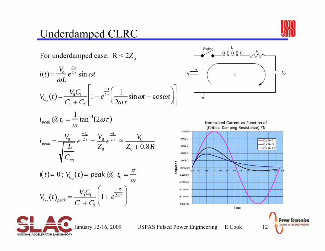
Underdamped CLRC
+C1
LR
C2
Switch
i(t)i(t) =Vo
ωLe
− t2τ sin ωt
VC2t( ) = V0C1
C1 + C2
1 − e− t2τ 1
2ωτsinωt − cosωt
⎛ ⎝ ⎜
⎞ ⎠ ⎟
⎡
⎣ ⎢ ⎢
⎤
⎦ ⎥ ⎥
ipeak @ t1 =1ω
tan−1 2ωτ( )
ipeak = V0
LCeq
e−t12τ = V0
Z0
e−t12τ ≅ V0
Z0 + 0.8R
i t( )= 0 ; VC2t( )= peak @ t0 = π
ω
VC2t( )peak = V0C1
C1 + C2
1+ e−π
2ωτ⎛
⎝ ⎜ ⎜
⎞
⎠ ⎟ ⎟
For underdamped case: R < 2Zo
January 12-16, 2009 USPAS Pulsed Power Engineering E Cook 13
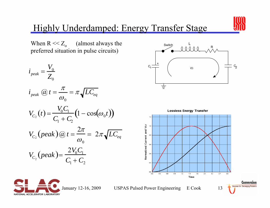
Highly Underdamped: Energy Transfer Stage
+C1
LR
C2
Switch
i(t)
When R << Zo (almost always the preferred situation in pulse circuits)
ipeak = V0
Z0
ipeak @ t = πω0
= π LCeq
VC2t( ) =
V0C1
C1 + C2
1 − cos ω0t( )( )
VC2peak( )@ t =
2πω0
= 2π LCeq
VC2peak( )=
2V0C1
C1 + C2
January 12-16, 2009 USPAS Pulsed Power Engineering C Burkhart 14
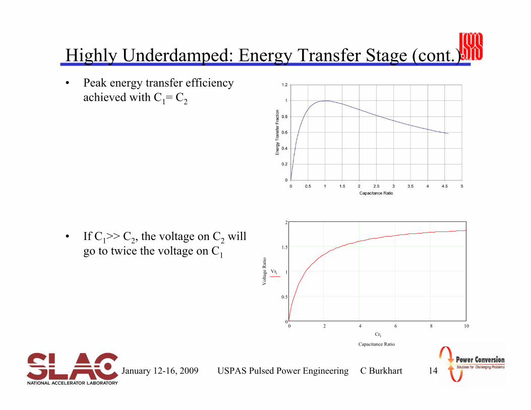
Highly Underdamped: Energy Transfer Stage (cont.)• Peak energy transfer efficiency
achieved with C1= C2
• If C1>> C2, the voltage on C2 will go to twice the voltage on C1
0 2 4 6 8 100
0.5
1
1.5
2
Capacitance Ratio
Vol
tage
Rat
ioVri
Cri
January 12-16, 2009 USPAS Pulsed Power Engineering E Cook 15
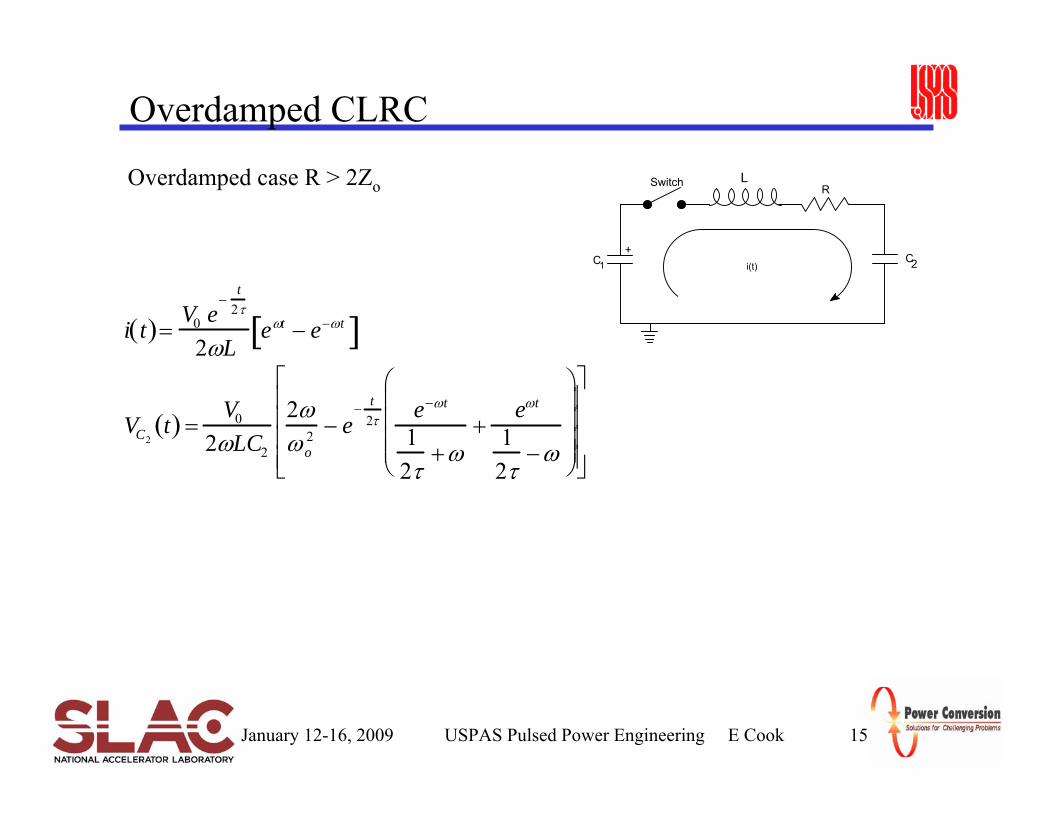
Overdamped CLRC
+C1
LR
C2
Switch
i(t)
Overdamped case R > 2Zo
i t( )=V0 e
−t
2τ
2ωLeωt − e−ωt[ ]
VC2t( ) =
V0
2ωLC2
2ωωo
2 − e− t
2τ e−ωt
12τ
+ω+
eωt
12τ
−ω
⎛
⎝
⎜ ⎜ ⎜ ⎜
⎞
⎠
⎟ ⎟ ⎟ ⎟
⎡
⎣
⎢ ⎢ ⎢ ⎢
⎤
⎦
⎥ ⎥ ⎥ ⎥
January 12-16, 2009 USPAS Pulsed Power Engineering TTU-PPSC 16
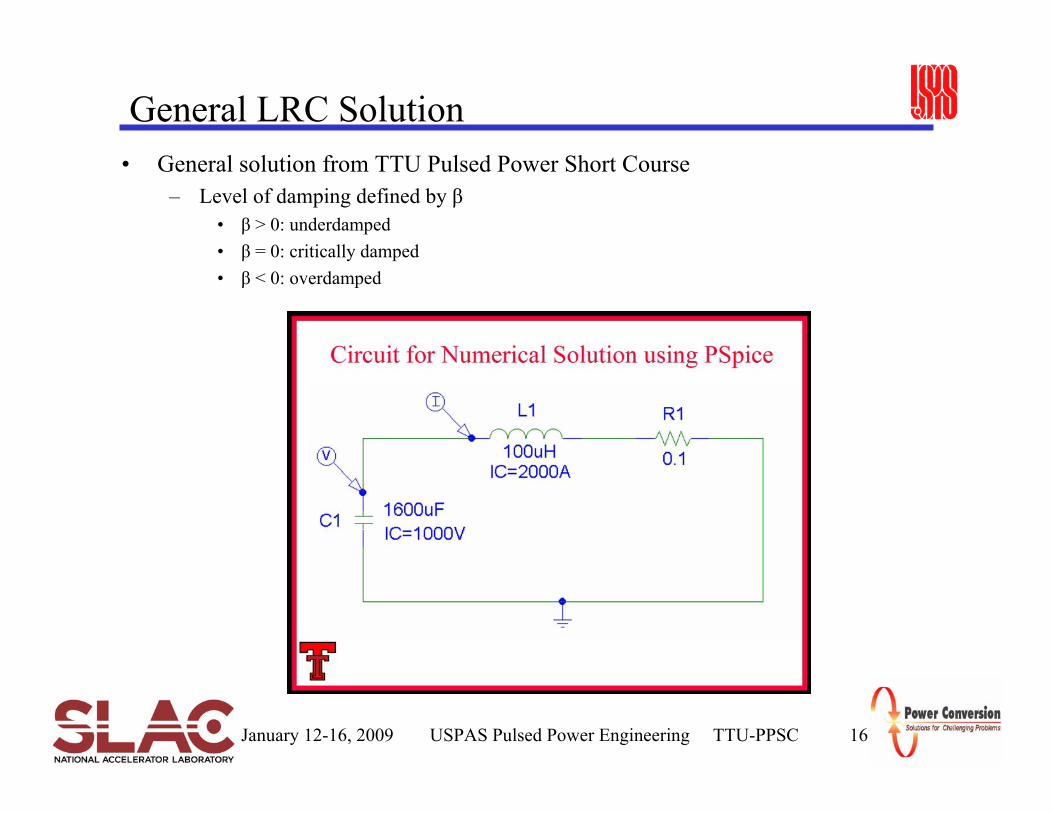
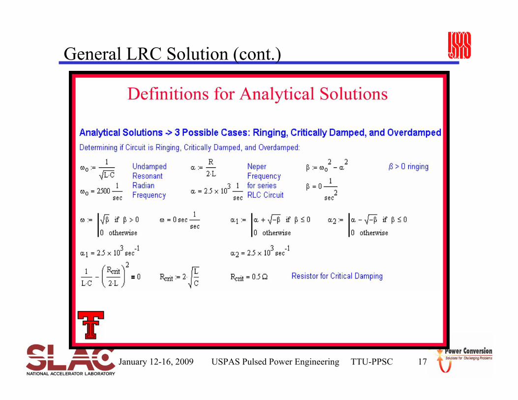
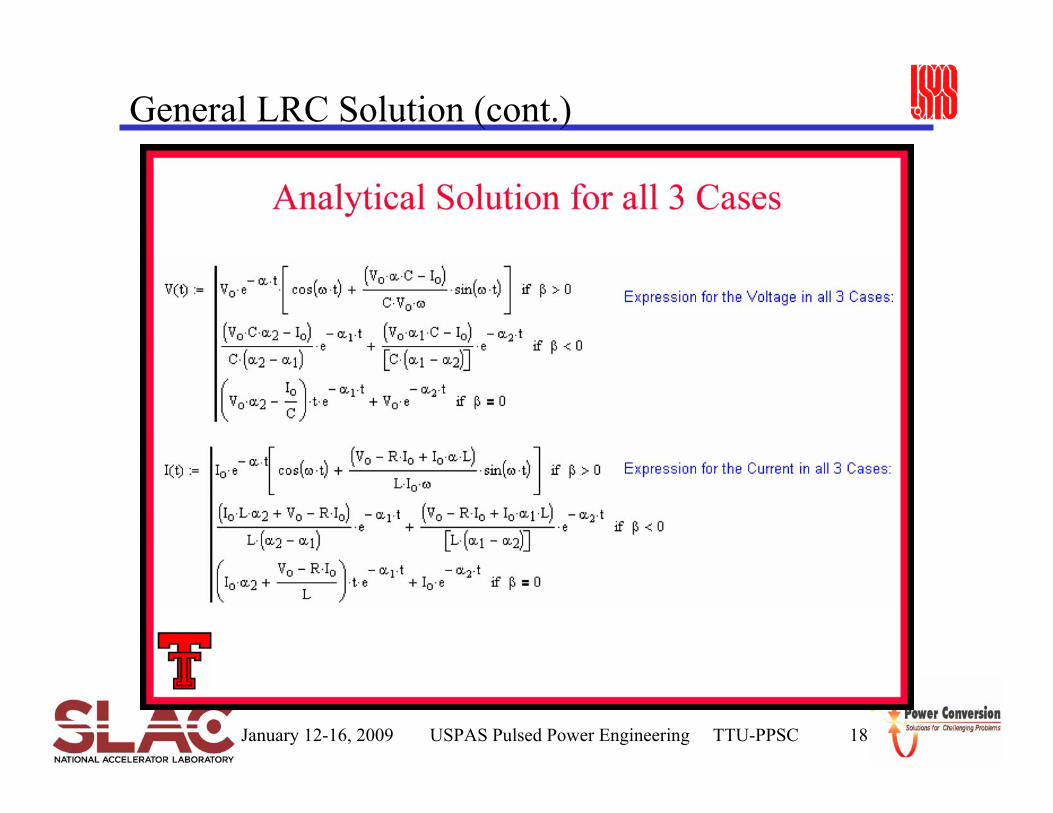
General LRC Solution• General solution from TTU Pulsed Power Short Course
– Level of damping defined by β• β > 0: underdamped• β = 0: critically damped• β < 0: overdamped
January 12-16, 2009 USPAS Pulsed Power Engineering TTU-PPSC 17
General LRC Solution (cont.)
January 12-16, 2009 USPAS Pulsed Power Engineering TTU-PPSC 18
General LRC Solution (cont.)
January 12-16, 2009 USPAS Pulsed Power Engineering Cook/Burkhart 19
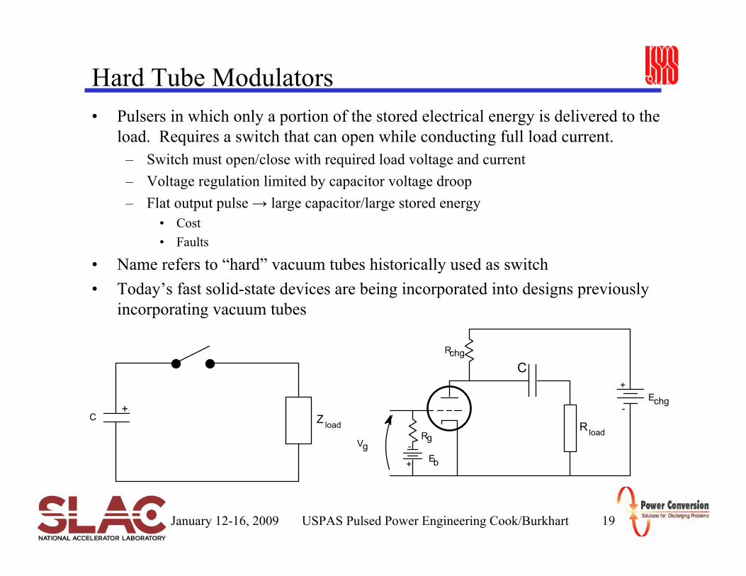
Hard Tube Modulators• Pulsers in which only a portion of the stored electrical energy is delivered to the
load. Requires a switch that can open while conducting full load current.– Switch must open/close with required load voltage and current– Voltage regulation limited by capacitor voltage droop– Flat output pulse → large capacitor/large stored energy
• Cost• Faults
• Name refers to “hard” vacuum tubes historically used as switch• Today’s fast solid-state devices are being incorporated into designs previously
incorporating vacuum tubes
+Z load
CRload
C
VgR
E+
-
b
g
Echg
+
-
Rchg
January 12-16, 2009 USPAS Pulsed Power Engineering Cook/Burkhart 20
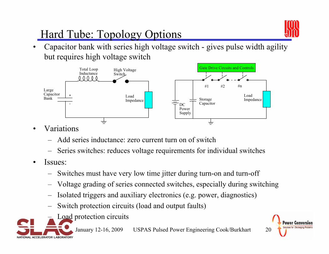
Hard Tube: Topology Options• Capacitor bank with series high voltage switch - gives pulse width agility
but requires high voltage switch
• Variations– Add series inductance: zero current turn on of switch– Series switches: reduces voltage requirements for individual switches
• Issues:– Switches must have very low time jitter during turn-on and turn-off – Voltage grading of series connected switches, especially during switching– Isolated triggers and auxiliary electronics (e.g. power, diagnostics)– Switch protection circuits (load and output faults)– Load protection circuits
High Voltage Switch
+
-
Load Impedance
Total Loop Inductance
Large Capacitor Bank
Load Impedance
#1 #2 #n
Gate Drive Circuits and Controls
DC Power Supply
Storage Capacitor
January 12-16, 2009 USPAS Pulsed Power Engineering E Cook 21
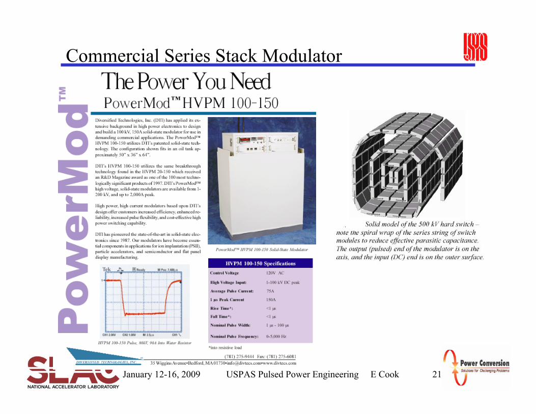
Commercial Series Stack Modulator
.
January 12-16, 2009 USPAS Pulsed Power Engineering C Burkhart 22
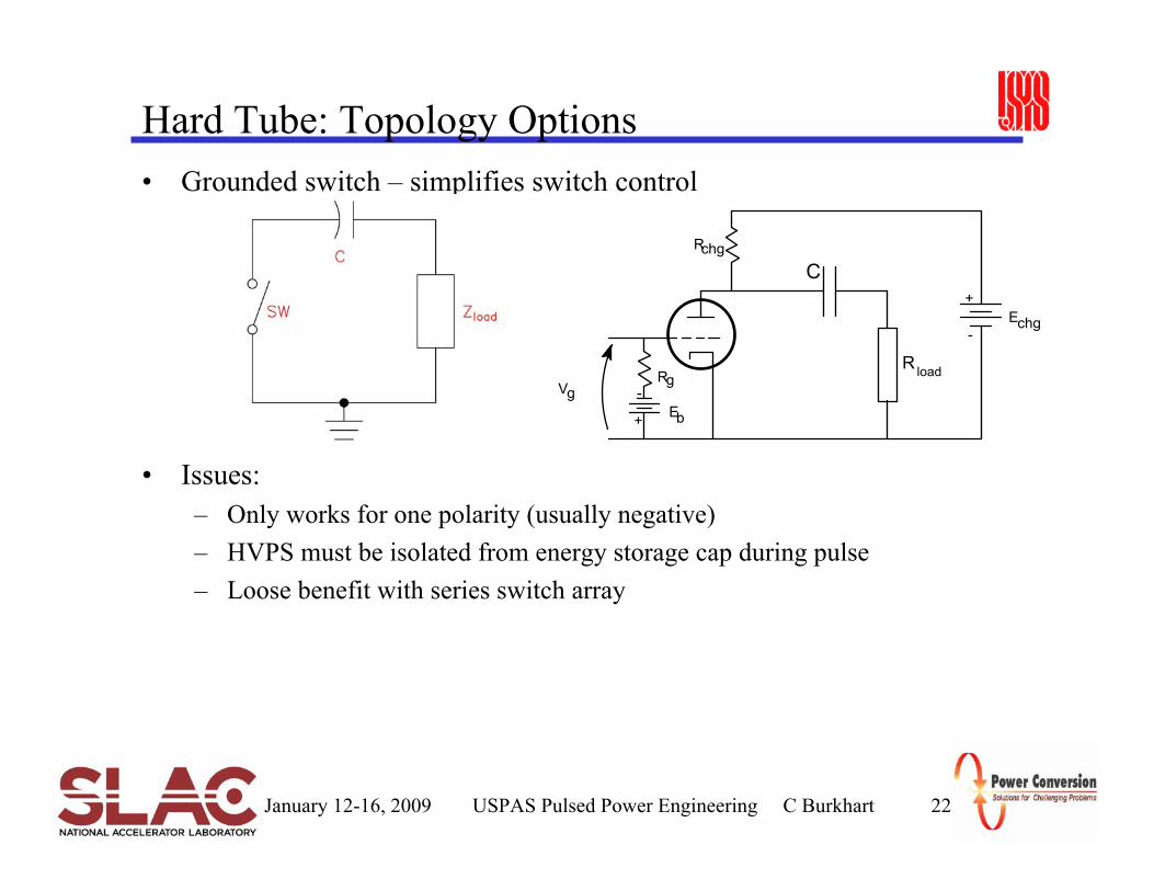
Hard Tube: Topology Options• Grounded switch – simplifies switch control
• Issues:– Only works for one polarity (usually negative)– HVPS must be isolated from energy storage cap during pulse– Loose benefit with series switch array
Rload
C
VgR
E+
-
b
g
Echg
+
-
Rchg
January 12-16, 2009 USPAS Pulsed Power Engineering Cook/Burkhart 23
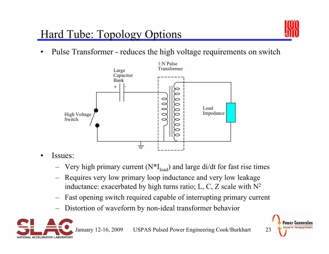
Hard Tube: Topology Options• Pulse Transformer - reduces the high voltage requirements on switch
• Issues:– Very high primary current (N*Iload) and large di/dt for fast rise times– Requires very low primary loop inductance and very low leakage
inductance: exacerbated by high turns ratio; L, C, Z scale with N2
– Fast opening switch required capable of interrupting primary current– Distortion of waveform by non-ideal transformer behavior
+ -
Load Impedance
Large Capacitor Bank
High Voltage Switch
1:N Pulse Transformer
January 12-16, 2009 USPAS Pulsed Power Engineering C Burkhart 24
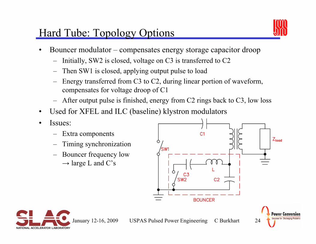
Hard Tube: Topology Options• Bouncer modulator – compensates energy storage capacitor droop
– Initially, SW2 is closed, voltage on C3 is transferred to C2– Then SW1 is closed, applying output pulse to load– Energy transferred from C3 to C2, during linear portion of waveform,
compensates for voltage droop of C1– After output pulse is finished, energy from C2 rings back to C3, low loss
• Used for XFEL and ILC (baseline) klystron modulators• Issues:
– Extra components– Timing synchronization– Bouncer frequency low
→ large L and C’s
January 12-16, 2009 USPAS Pulsed Power Engineering C Burkhart 25
Line-Type Modulators• Based on the properties of transmission lines as pulse generating devices• Advantages
– Minimum stored energy, 100% → load (neglecting losses)• Voltage fed, capacitive storage (E-field), closing switch• Current fed, inductive storage (B-field), opening switch
– Fault (short circuit) current ≤ twice operating current (matched load)– Relatively simple to design and fabricate, inexpensive– Switch action is closing OR opening, but not both
• Disadvantages– Fixed (and limited range) output pulse length– Fixed (and limited range) output pulse impedance
• Output pulse shape dependent on relative modulator/load impedance• Zload< Zpulser → voltage reversal, may damage switch or other components
– Switch operates at twice the voltage (or current) delivered to load– Must be fully recharged between pulses: may be difficult at high PRF
January 12-16, 2009 USPAS Pulsed Power Engineering C Burkhart 26
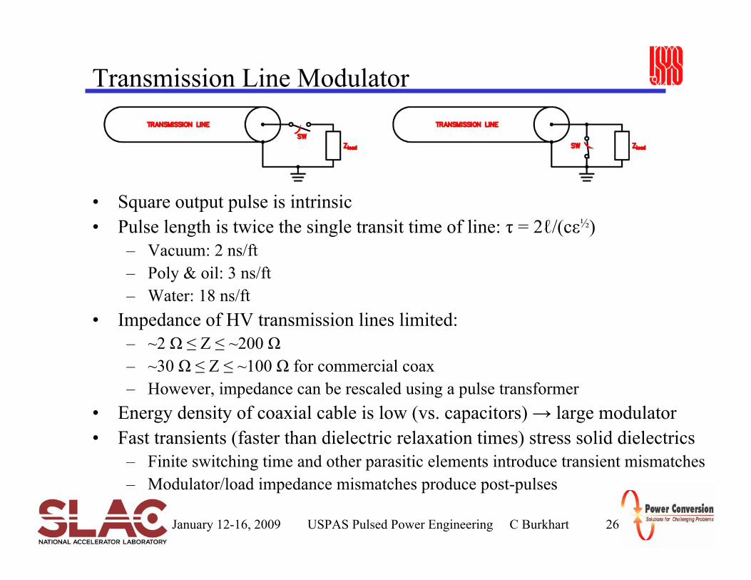
Transmission Line Modulator
• Square output pulse is intrinsic• Pulse length is twice the single transit time of line: τ = 2ℓ/(cε½)
– Vacuum: 2 ns/ft– Poly & oil: 3 ns/ft– Water: 18 ns/ft
• Impedance of HV transmission lines limited:– ~2 Ω ≤ Z ≤ ~200 Ω– ~30 Ω ≤ Z ≤ ~100 Ω for commercial coax– However, impedance can be rescaled using a pulse transformer
• Energy density of coaxial cable is low (vs. capacitors) → large modulator• Fast transients (faster than dielectric relaxation times) stress solid dielectrics
– Finite switching time and other parasitic elements introduce transient mismatches– Modulator/load impedance mismatches produce post-pulses
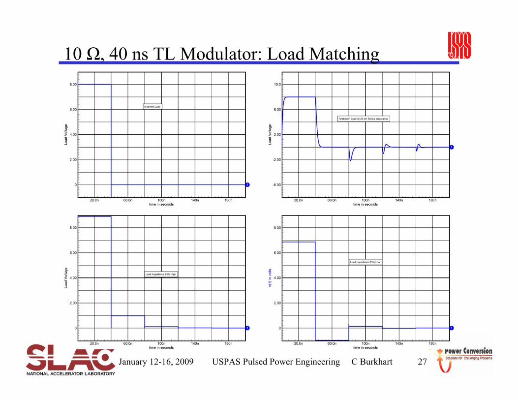
January 12-16, 2009 USPAS Pulsed Power Engineering C Burkhart 27
10 Ω, 40 ns TL Modulator: Load Matching
January 12-16, 2009 USPAS Pulsed Power Engineering E Cook 28
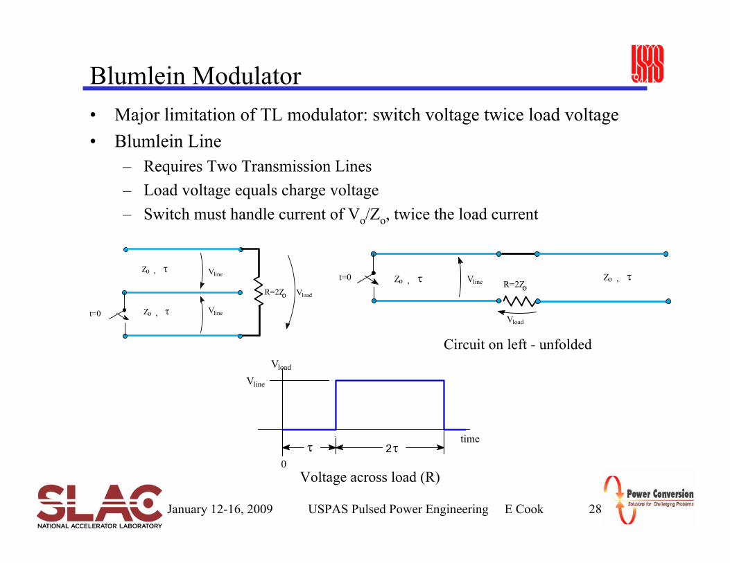
Blumlein Modulator• Major limitation of TL modulator: switch voltage twice load voltage• Blumlein Line
– Requires Two Transmission Lines– Load voltage equals charge voltage– Switch must handle current of Vo/Zo, twice the load current
R=2ZoZ τo , Z τo ,t=0 Vline
Vload
2τtime
τ0
Vload
Vline
Circuit on left - unfolded
Voltage across load (R)
R=2Zo
Z τo ,
Z τo ,
t=0
Vline
Vline
Vload
January 12-16, 2009 USPAS Pulsed Power Engineering C Burkhart 29
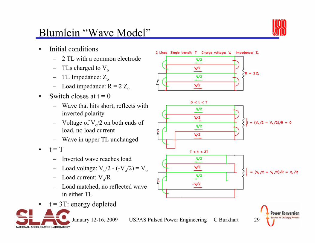
Blumlein “Wave Model”• Initial conditions
– 2 TL with a common electrode– TLs charged to Vo
– TL Impedance: Zo
– Load impedance: R = 2 Zo
• Switch closes at t = 0– Wave that hits short, reflects with
inverted polarity– Voltage of Vo/2 on both ends of
load, no load current– Wave in upper TL unchanged
• t = T– Inverted wave reaches load– Load voltage: Vo/2 - (-Vo/2) = Vo
– Load current: Vo/R– Load matched, no reflected wave
in either TL• t = 3T: energy depleted
January 12-16, 2009 USPAS Pulsed Power Engineering J Mankowski 30
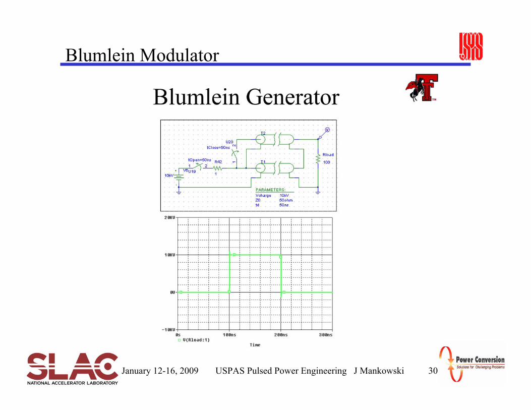
Blumlein Modulator
January 12-16, 2009 USPAS Pulsed Power Engineering C Burkhart 31
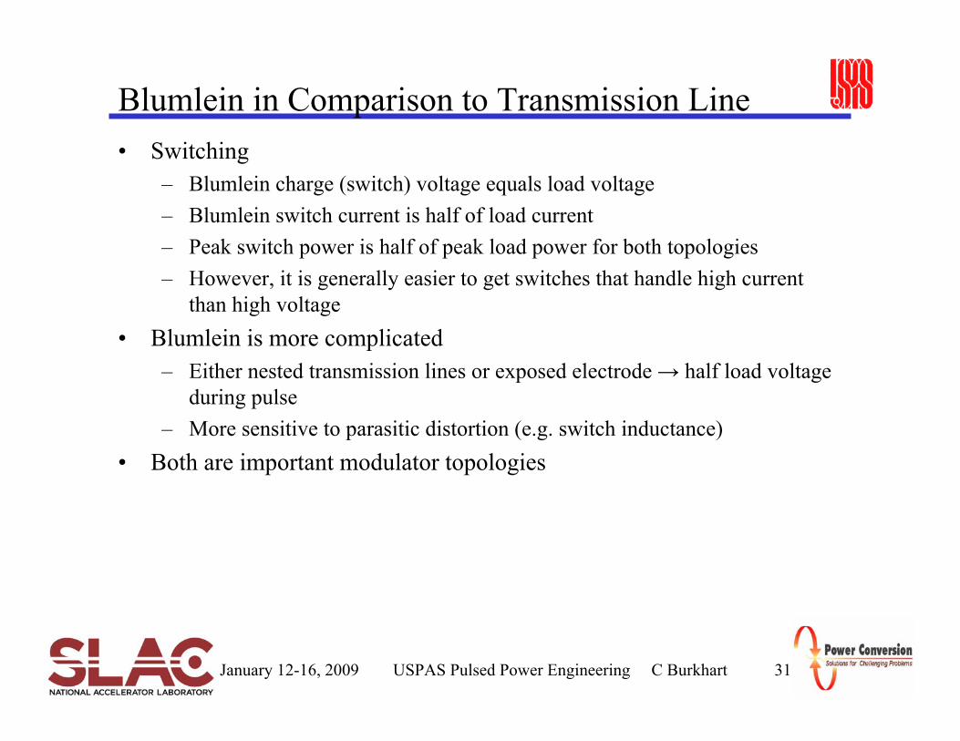
Blumlein in Comparison to Transmission Line• Switching
– Blumlein charge (switch) voltage equals load voltage– Blumlein switch current is half of load current– Peak switch power is half of peak load power for both topologies– However, it is generally easier to get switches that handle high current
than high voltage• Blumlein is more complicated
– Either nested transmission lines or exposed electrode → half load voltage during pulse
– More sensitive to parasitic distortion (e.g. switch inductance)• Both are important modulator topologies
January 12-16, 2009 USPAS Pulsed Power Engineering E Cook 32
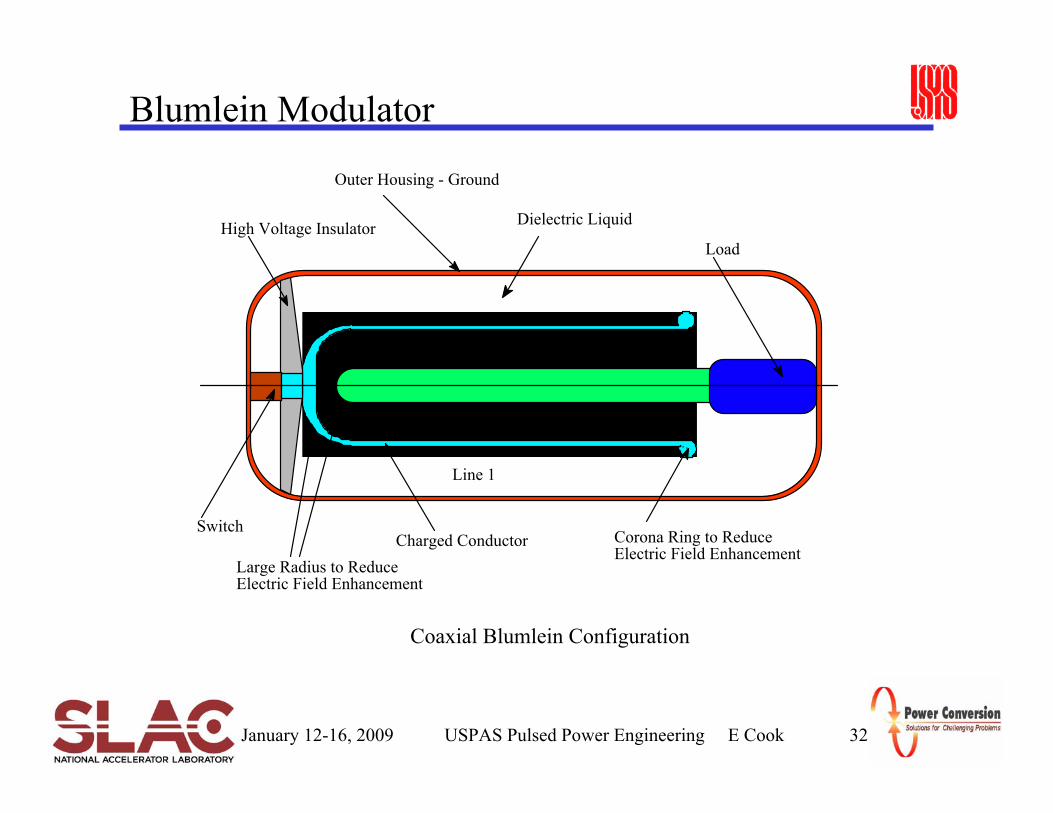
Blumlein Modulator
SwitchCharged Conductor
Line 1
Line 2
LoadHigh Voltage Insulator Dielectric Liquid
Coaxial Blumlein Configuration
Corona Ring to Reduce Electric Field Enhancement
Outer Housing - Ground
Large Radius to Reduce Electric Field Enhancement
January 12-16, 2009 USPAS Pulsed Power Engineering C Burkhart 33
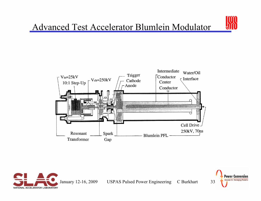
Advanced Test Accelerator Blumlein Modulator
January 12-16, 2009 USPAS Pulsed Power Engineering C Burkhart 34
Pulse Forming Networks (PFNs)• The maximum pulse duration of transmission line pulsers is limited by the
physical length of the line, at 3 ns/ft, a 1 μs TL would be 330’ long• Transmission line can be approximated by an LC array
– Higher energy density in capacitors– Higher energy density in solenoidal inductors– PFNs can produce long duration pulses in a compact package
• Design equations– Z = (L/C)0.5
– τ = 2N(LC)0.5 (output pulse length)– For N-stages of inductance, L, and capacitance, C
• However, the discrete element model of the TL is only accurate as the number of stages, N →∞
• Example– N = 7– Z = 10Ω– Τ = 1 μs
• C = 7.14 nF• L = 0.714 μH
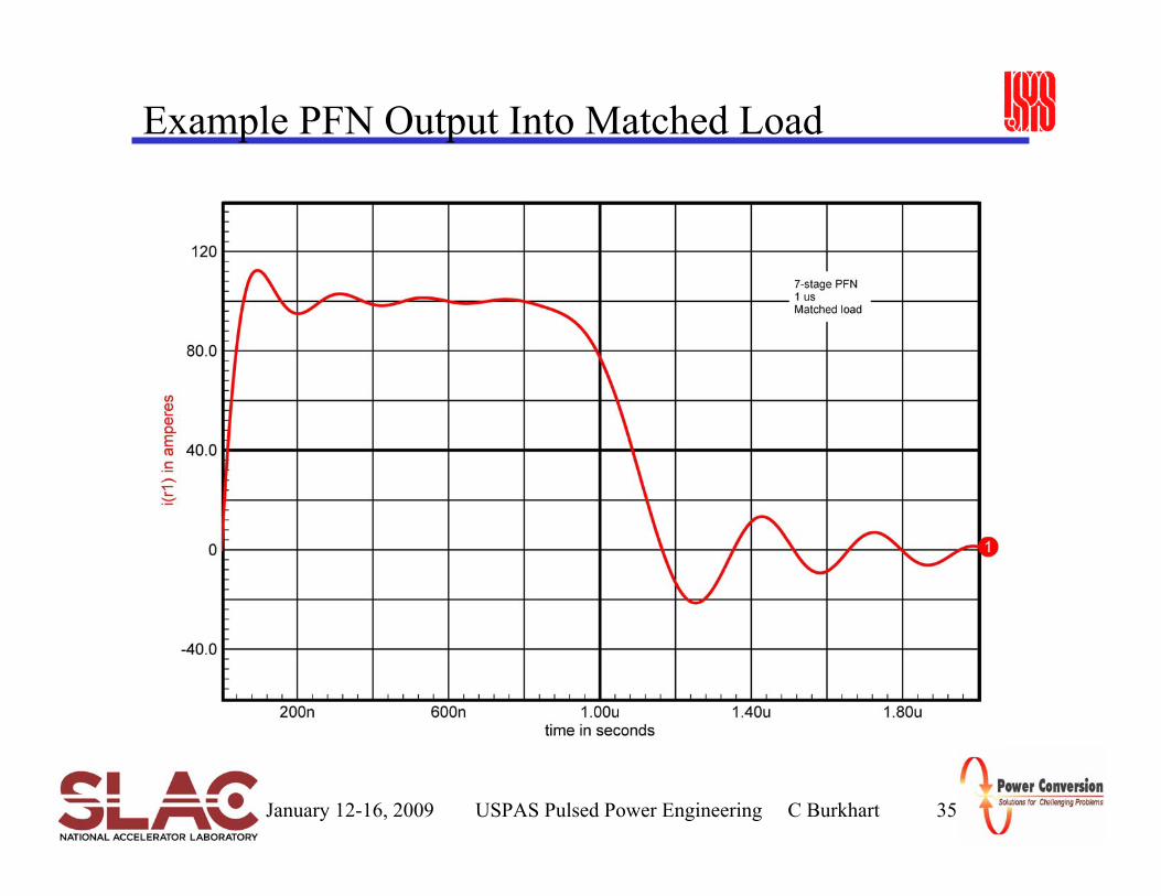
January 12-16, 2009 USPAS Pulsed Power Engineering C Burkhart 35
Example PFN Output Into Matched Load
January 12-16, 2009 USPAS Pulsed Power Engineering C Burkhart 36
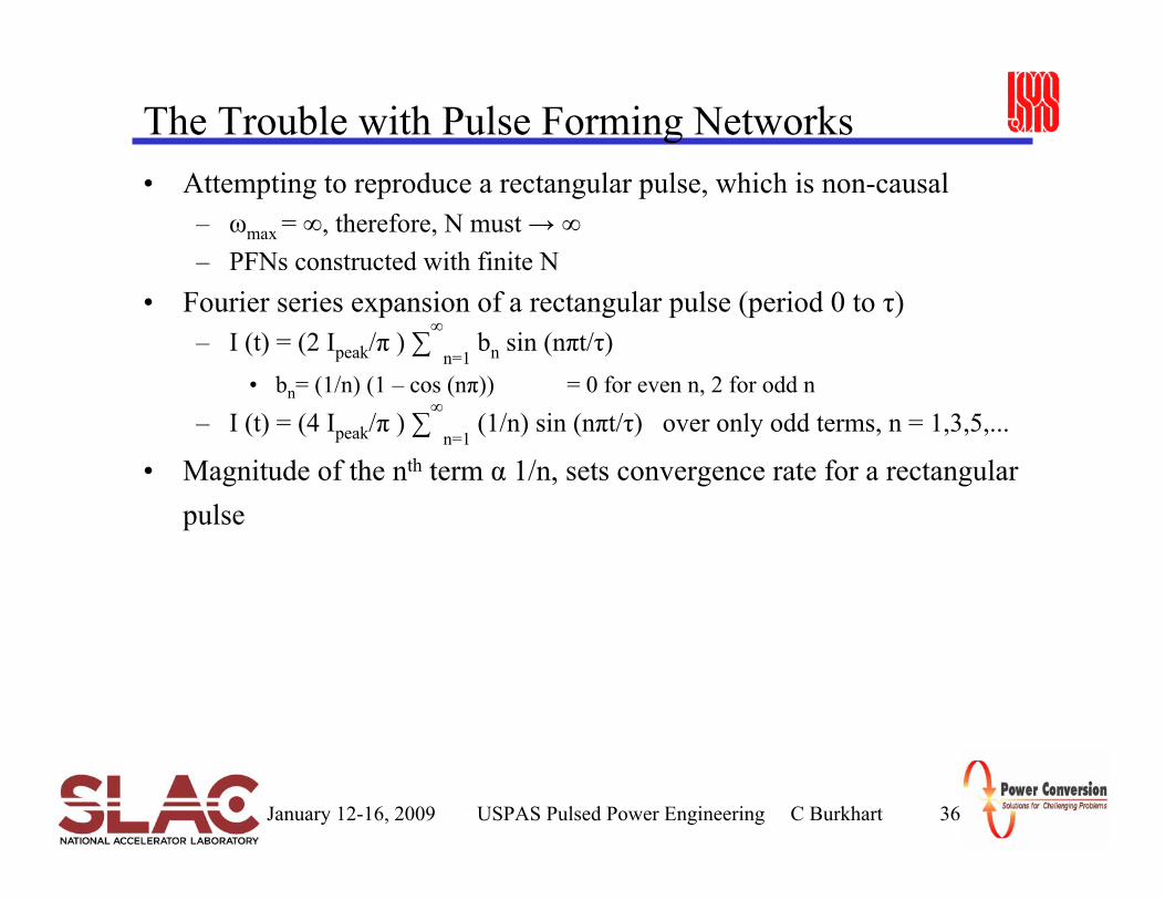
The Trouble with Pulse Forming Networks• Attempting to reproduce a rectangular pulse, which is non-causal
– ωmax = ∞, therefore, N must → ∞– PFNs constructed with finite N
• Fourier series expansion of a rectangular pulse (period 0 to τ)– I (t) = (2 Ipeak/π ) ∑
∞
n=1bn sin (nπt/τ)
• bn= (1/n) (1 – cos (nπ)) = 0 for even n, 2 for odd n
– I (t) = (4 Ipeak/π ) ∑∞
n=1(1/n) sin (nπt/τ) over only odd terms, n = 1,3,5,...
• Magnitude of the nth term α 1/n, sets convergence rate for a rectangular pulse
January 12-16, 2009 USPAS Pulsed Power Engineering C Burkhart 37
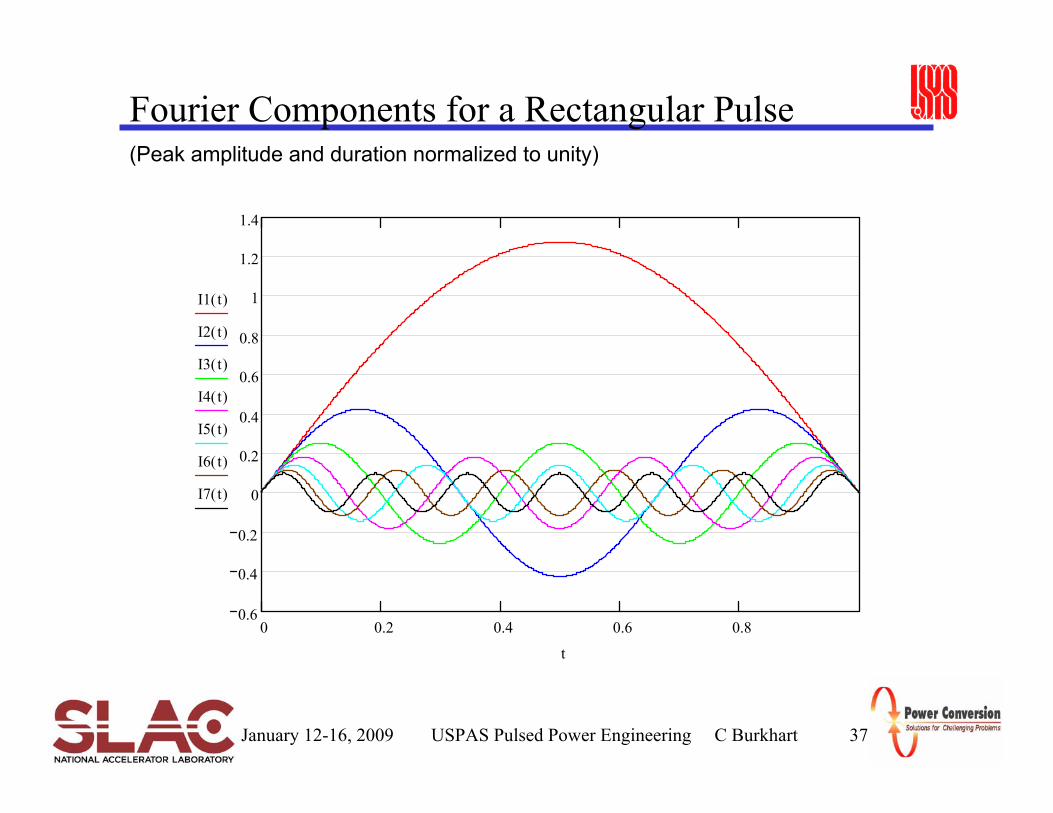
Fourier Components for a Rectangular Pulse
0 0.2 0.4 0.6 0.80.6
0.4
0.2
0
0.2
0.4
0.6
0.8
1
1.2
1.4
I1 t( )
I2 t( )
I3 t( )
I4 t( )
I5 t( )
I6 t( )
I7 t( )
t
(Peak amplitude and duration normalized to unity)
January 12-16, 2009 USPAS Pulsed Power Engineering C Burkhart 38
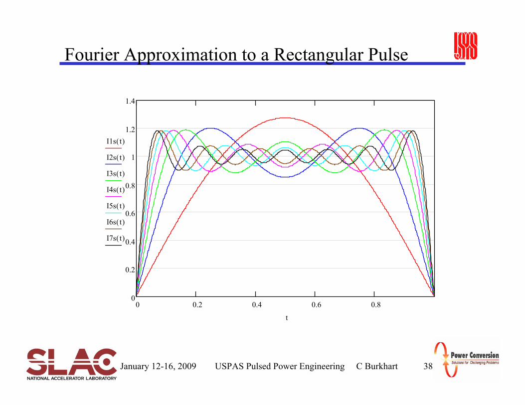
Fourier Approximation to a Rectangular Pulse
0 0.2 0.4 0.6 0.80
0.2
0.4
0.6
0.8
1
1.2
1.4
I1s t( )
I2s t( )
I3s t( )
I4s t( )
I5s t( )
I6s t( )
I7s t( )
t
January 12-16, 2009 USPAS Pulsed Power Engineering C Burkhart 39
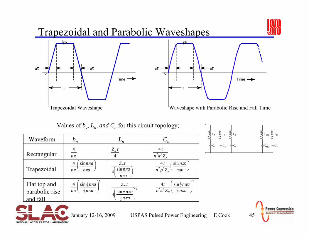
Guillemin Networks: The Solution to “The Trouble with PFNs”
• E.A. Guillemin recognized that the discontinuities due to– Zero rise/fall time, and– Corners at the start/stop of the rise and fall
are the source of the high frequency components that challenge PFN design. “Communication Networks,” 1935
• Further, since such a perfect waveform cannot be generated by this method, that better results can be obtained by intentionally design for finite rise/fall times (i.e. trapezoidal pulse) and by rounding the corners (i.e. parabolic rise/fall pulse)
• Fourier decomposition of these waveforms shows faster convergence– Trapezoidal: nth term α 1/n2
– Parabolic: nth term α 1/n3
January 12-16, 2009 USPAS Pulsed Power Engineering E Cook 40
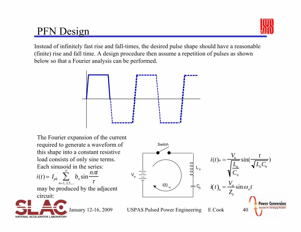
PFN DesignInstead of infinitely fast rise and fall-times, the desired pulse shape should have a reasonable (finite) rise and fall time. A design procedure then assume a repetition of pulses as shown below so that a Fourier analysis can be performed.
The Fourier expansion of the current required to generate a waveform of this shape into a constant resistive load consists of only sine terms. Each sinusoid in the series:
may be produced by the adjacent circuit:
i(t)n =Vn
Ln
Cn
sin(t
LnCn
)
i t( )n = Vn
Zn
sinωot
Switch
nV
i(t)n Cn
Ln
i(t) = Ipk bn sinnπtτn=1, 3,5,...
∞
∑
January 12-16, 2009 USPAS Pulsed Power Engineering E Cook 41
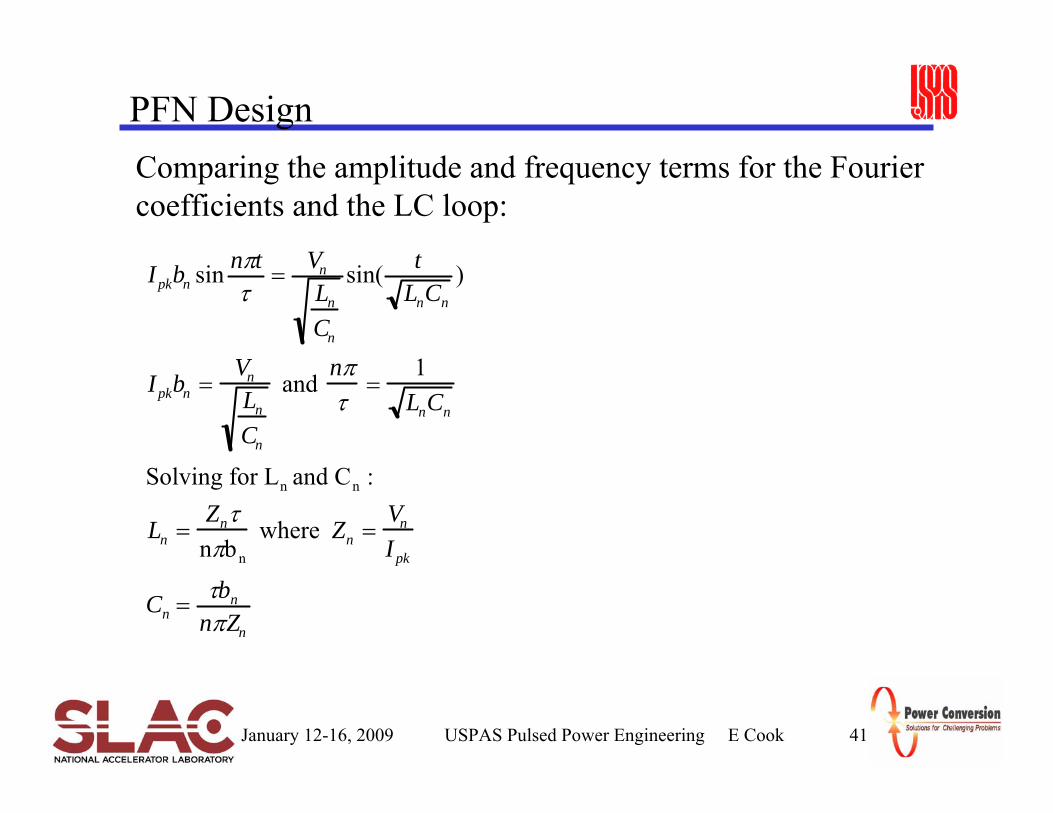
PFN DesignComparing the amplitude and frequency terms for the Fourier coefficients and the LC loop:
Ipkbn sin nπtτ
= Vn
Ln
Cn
sin( tLnCn
)
Ipkbn =Vn
Ln
Cn
and nπτ
=1
LnCn
Solving for Ln and Cn :
Ln =Znτ
nπbn
where Zn =Vn
Ipk
Cn = τbn
nπZn
January 12-16, 2009 USPAS Pulsed Power Engineering E Cook 42
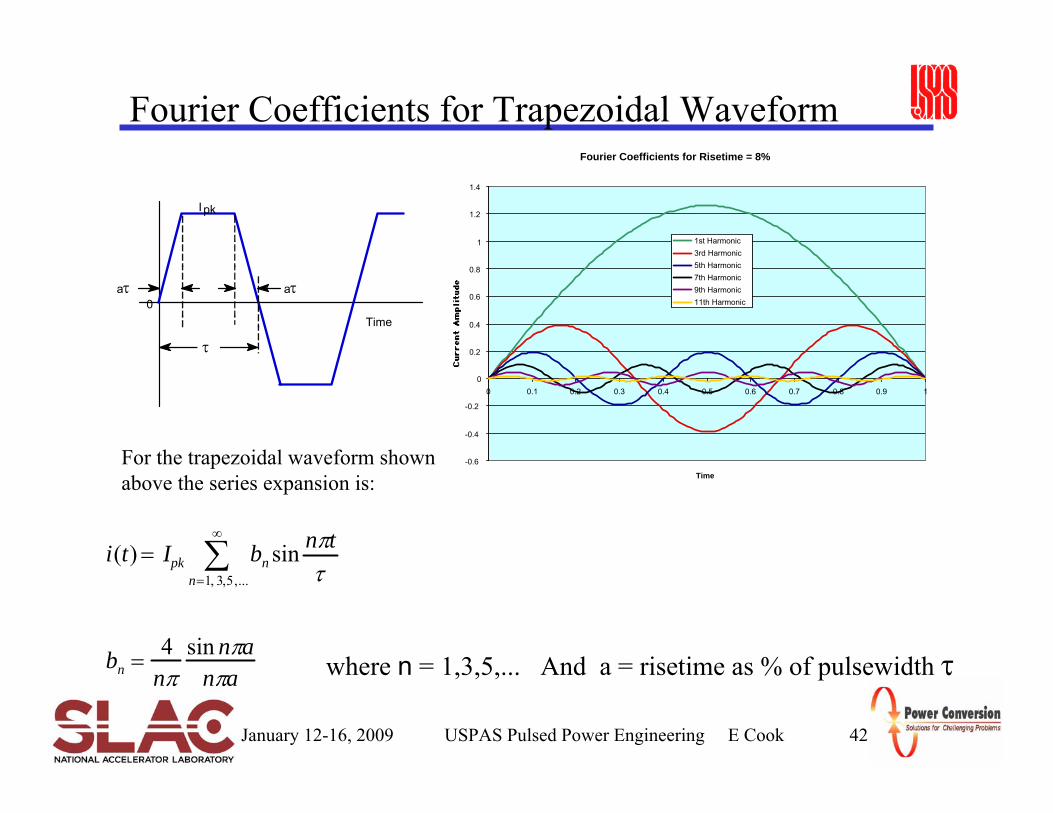
Fourier Coefficients for Trapezoidal WaveformFourier Coefficients for Risetime = 8%
-0.6
-0.4
-0.2
0
0.2
0.4
0.6
0.8
1
1.2
1.4
0 0.1 0.2 0.3 0.4 0.5 0.6 0.7 0.8 0.9 1
Time
1st Harmonic3rd Harmonic5th Harmonic7th Harmonic9th Harmonic11th Harmonic
For the trapezoidal waveform shownabove the series expansion is:
i(t) = Ipk bn sin nπtτn=1, 3,5,...
∞
∑
bn = 4nπ
sin nπanπa where n = 1,3,5,... And a = risetime as % of pulsewidth τ
I pk
Time0
aτ
τ
aτ
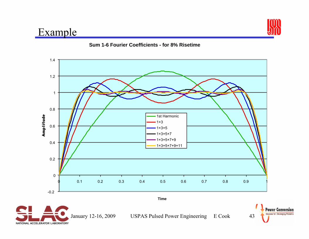
January 12-16, 2009 USPAS Pulsed Power Engineering E Cook 43
ExampleSum 1-6 Fourier Coefficients - for 8% Risetime
-0.2
0
0.2
0.4
0.6
0.8
1
1.2
1.4
0 0.1 0.2 0.3 0.4 0.5 0.6 0.7 0.8 0.9 1
Time
1st Harmonic1+31+3+51+3+5+7 1+3+5+7+91+3+5+7+9+11
January 12-16, 2009 USPAS Pulsed Power Engineering E Cook 44
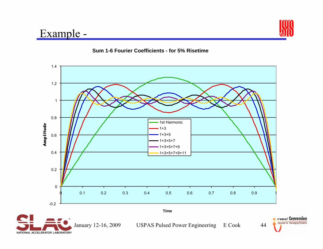
Example -Sum 1-6 Fourier Coefficients - for 5% Risetime
-0.2
0
0.2
0.4
0.6
0.8
1
1.2
1.4
0 0.1 0.2 0.3 0.4 0.5 0.6 0.7 0.8 0.9 1
Time
1st Harmonic1+31+3+51+3+5+7 1+3+5+7+91+3+5+7+9+11
January 12-16, 2009 USPAS Pulsed Power Engineering E Cook 45
Trapezoidal and Parabolic WaveshapesIpk
Time0
aτ
τ
aτ
Ipk
Time0
aτ
τ
aτ
C
L
1
1
C
L
3
3
C
L
5
5
C
L
M-2
M-2
C
L
M
M
Values of bv, Ln, and Cn for this circuit topology;
Waveform bn Ln Cn
Rectangular
Trapezoidal
Flat top and parabolic riseand fall
4nπ
ZNτ4
4τn2π 2 ZN
4nπ
sinnπanπa
⎛ ⎝ ⎜
⎞ ⎠ ⎟
ZN t
4 sin nπanπa
⎛ ⎝ ⎜
⎞ ⎠ ⎟
4τ
n2 p2 ZN
sin nπanπa
⎛ ⎝ ⎜
⎞ ⎠ ⎟
4nπ
sin 12 nπa
12 nπa
⎛
⎝ ⎜ ⎜
⎞
⎠ ⎟ ⎟
2
ZNτ
4 sin 12 nπa
12 nπa
⎛
⎝ ⎜ ⎜
⎞
⎠ ⎟ ⎟
2 4τn2π 2 ZN
sin 12 nπa
12 nπa
⎛
⎝ ⎜ ⎜
⎞
⎠ ⎟ ⎟
2
Trapezoidal Waveshape Waveshape with Parabolic Rise and Fall Time
January 12-16, 2009 USPAS Pulsed Power Engineering E Cook 46
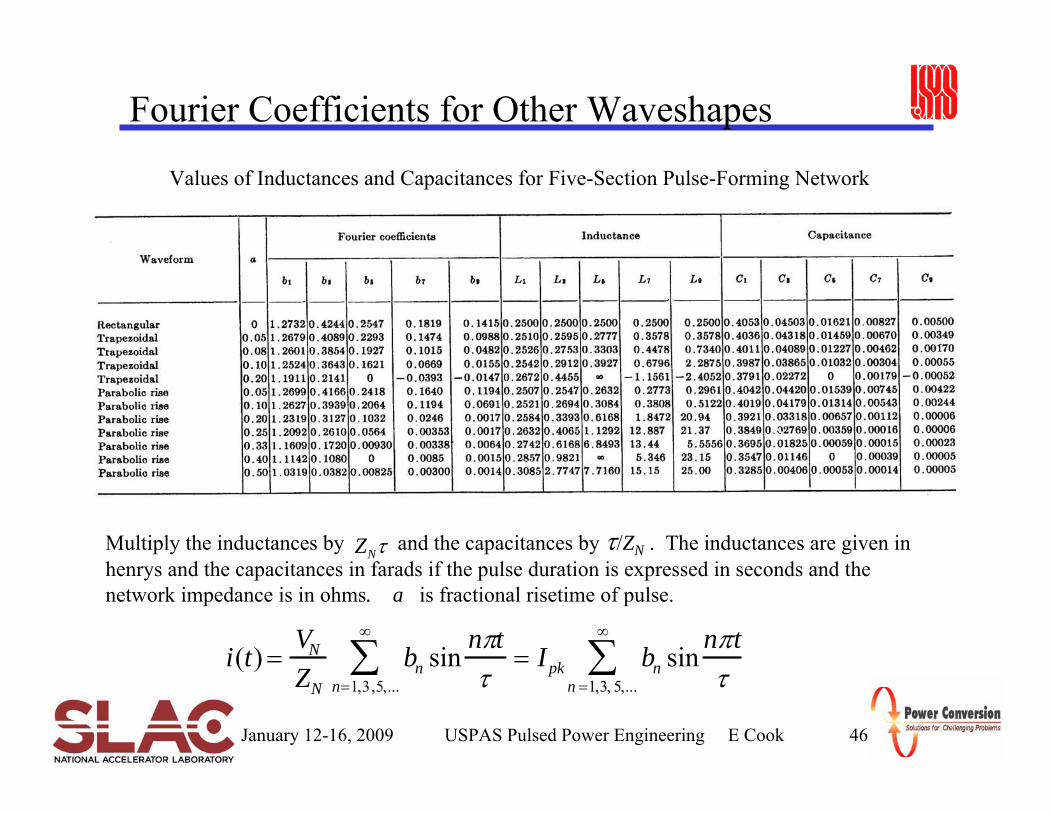
Fourier Coefficients for Other Waveshapes
Values of Inductances and Capacitances for Five-Section Pulse-Forming Network
Multiply the inductances by and the capacitances by τ/ZN . The inductances are given in henrys and the capacitances in farads if the pulse duration is expressed in seconds and the network impedance is in ohms. a is fractional risetime of pulse.
ZNτ
i(t) =VN
ZN
bn sinnπtτn=1,3,5,...
∞
∑ = Ipk bn sinnπtτn =1,3, 5,...
∞
∑
January 12-16, 2009 USPAS Pulsed Power Engineering E Cook 47
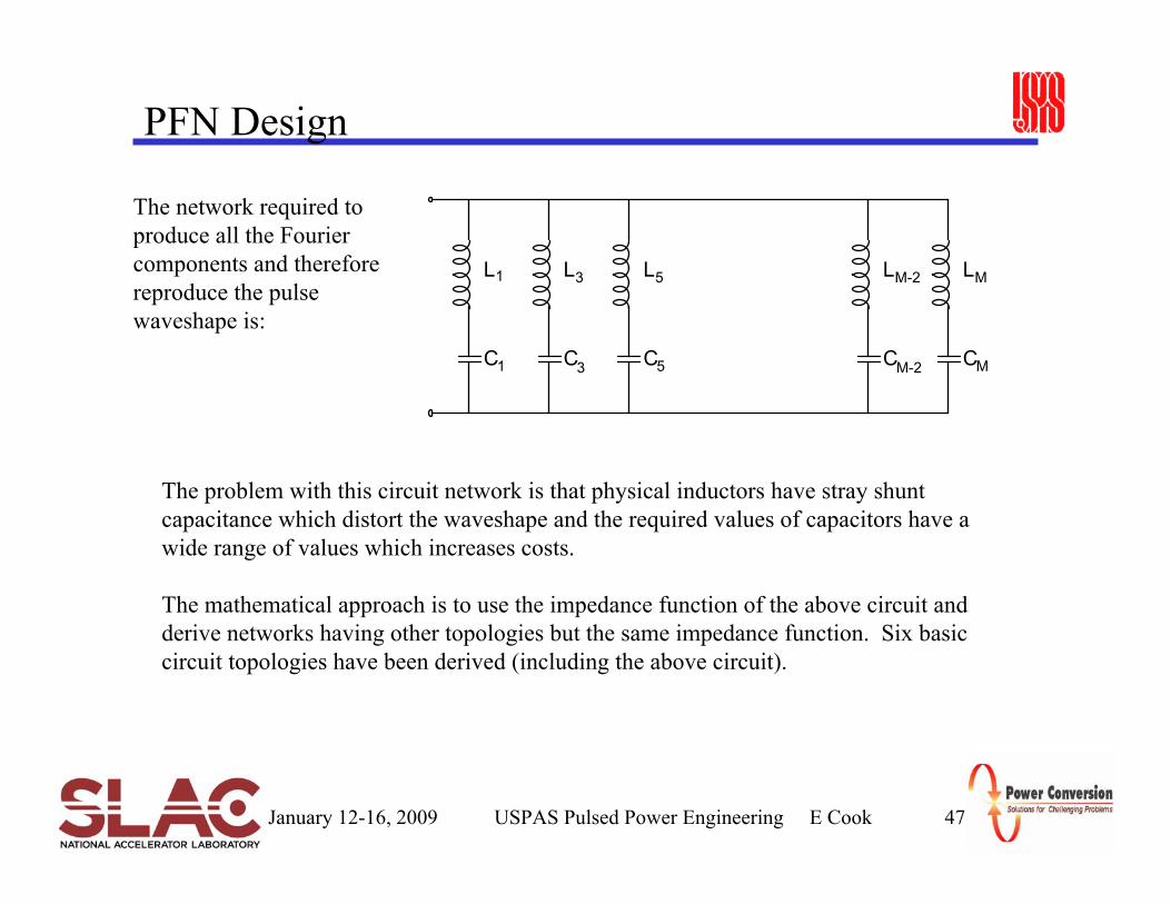
PFN Design
The network required to produce all the Fourier components and therefore reproduce the pulse waveshape is:
The problem with this circuit network is that physical inductors have stray shunt capacitance which distort the waveshape and the required values of capacitors have a wide range of values which increases costs.
The mathematical approach is to use the impedance function of the above circuit and derive networks having other topologies but the same impedance function. Six basic circuit topologies have been derived (including the above circuit).
C
L
1
1
C
L
3
3
C
L
5
5
C
L
M-2
M-2
C
L
M
M
January 12-16, 2009 USPAS Pulsed Power Engineering E Cook 48
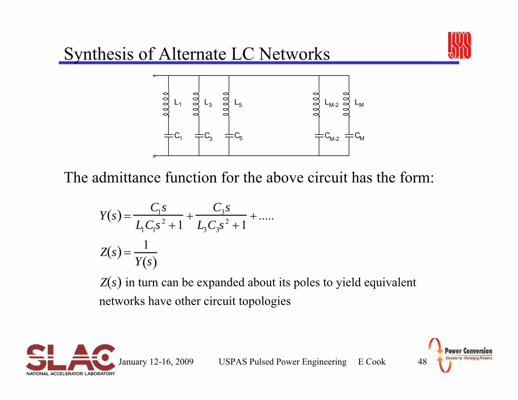
Synthesis of Alternate LC Networks
The admittance function for the above circuit has the form:
C
L
1
1
C
L
3
3
C
L
5
5
C
L
M-2
M-2
C
L
M
M
Y s( ) =C1s
L1C1s2 +1
+C3s
L3C3s2 +1
+ .....
Z s( ) = 1Y s( )
Z s( ) in turn can be expanded about its poles to yield equivalent networks have other circuit topologies
January 12-16, 2009 USPAS Pulsed Power Engineering C Burkhart 49
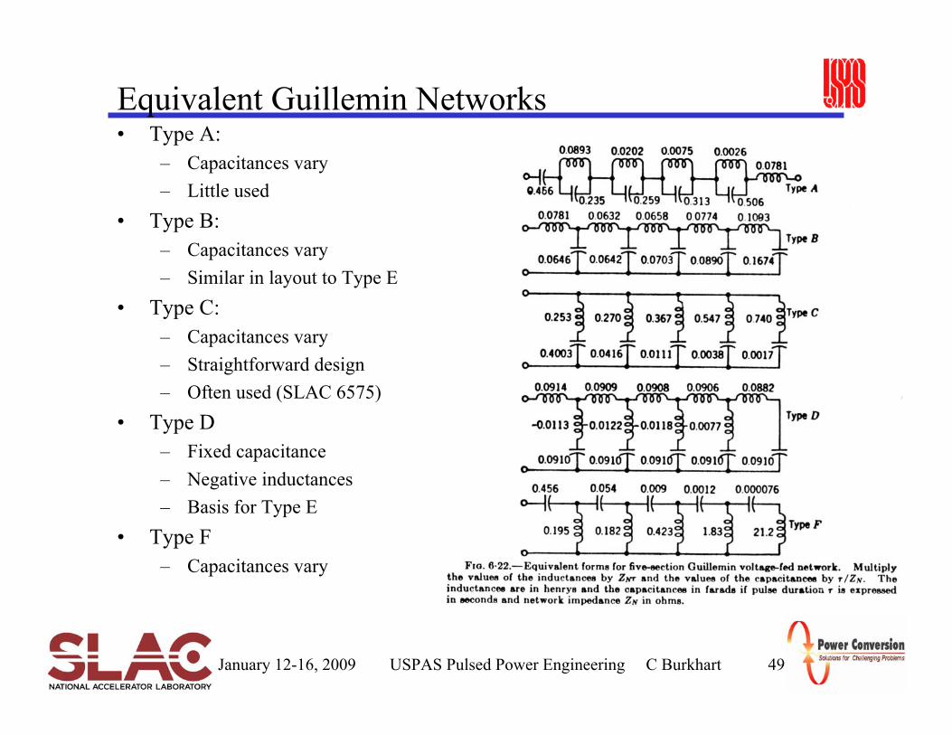
Equivalent Guillemin Networks• Type A:
– Capacitances vary– Little used
• Type B: – Capacitances vary– Similar in layout to Type E
• Type C: – Capacitances vary– Straightforward design– Often used (SLAC 6575)
• Type D– Fixed capacitance– Negative inductances– Basis for Type E
• Type F– Capacitances vary
January 12-16, 2009 USPAS Pulsed Power Engineering Cook/Burkhart 50
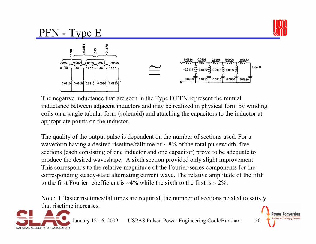
PFN - Type E
The negative inductance that are seen in the Type D PFN represent the mutual inductance between adjacent inductors and may be realized in physical form by winding coils on a single tubular form (solenoid) and attaching the capacitors to the inductor at appropriate points on the inductor.
The quality of the output pulse is dependent on the number of sections used. For a waveform having a desired risetime/falltime of ~ 8% of the total pulsewidth, five sections (each consisting of one inductor and one capacitor) prove to be adequate to produce the desired waveshape. A sixth section provided only slight improvement. This corresponds to the relative magnitude of the Fourier-series components for the corresponding steady-state alternating current wave. The relative amplitude of the fifth to the first Fourier coefficient is ~4% while the sixth to the first is ~ 2%.
Note: If faster risetimes/falltimes are required, the number of sections needed to satisfy that risetime increases.
=~

January 12-16, 2009 USPAS Pulsed Power Engineering Cook/Burkhart 51
Type E PFN- Practical Design Parameters• For :
– PFN Characteristic Impedance = Zo
– PFN Output Pulse Width = 2τ• where LN = total PFN inductance and
CN = total PFN capacitance– The total PFN inductance (including mutual inductances) and capacitance
is divided equally between the number of sections. – Empirical data have shown that the best waveshape can be achieved when
the end inductors should have ~20-30% more self inductance. The mutual inductance should be approximately 15% of the self inductances.
• Bottom line: don’t bust your pick designing a “perfect” PFN– Capacitance values vary from can-to-can and with time– Inductor values are never quite as designed– Strays; inductance, capacitance, resistance, distort the waveform– and should you somehow overcome all of the foregoing, you can be
certain that the technicians will “tune” the PFN and your “perfect”waveform will be but a memory
LN
CN
τ =
Zo =
LNCN
January 12-16, 2009 USPAS Pulsed Power Engineering E Cook 52
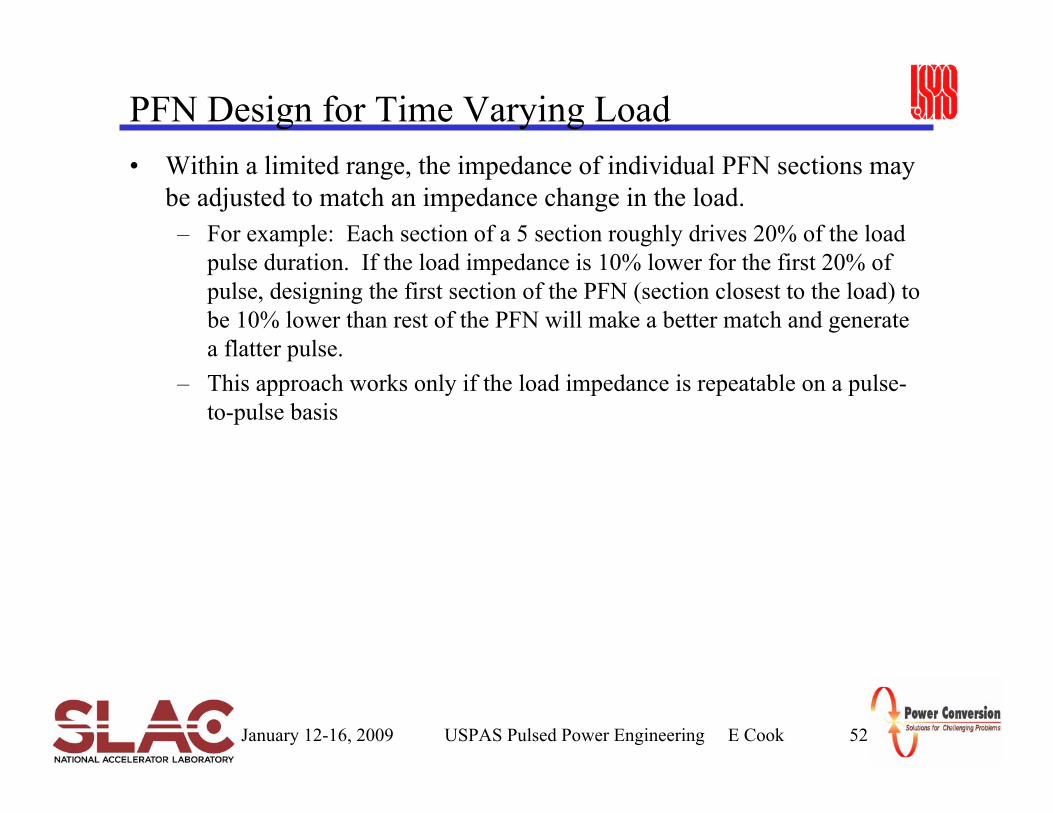
PFN Design for Time Varying Load• Within a limited range, the impedance of individual PFN sections may
be adjusted to match an impedance change in the load.– For example: Each section of a 5 section roughly drives 20% of the load
pulse duration. If the load impedance is 10% lower for the first 20% of pulse, designing the first section of the PFN (section closest to the load) to be 10% lower than rest of the PFN will make a better match and generate a flatter pulse.
– This approach works only if the load impedance is repeatable on a pulse-to-pulse basis

January 12-16, 2009 USPAS Pulsed Power Engineering C Burkhart 53
PFN: Practical Issues• Switch: In addition to voltage and peak current requirements, must also be able
to handle peak dI/dt (highest frequency components will be smaller magnitude and may be difficult to observe)
– SLC modifications to 6575 doubled dI/dt– Even with 2 thyratrons, short tube life– Solved by adding “anode reactor” (magnetic switch in series with tube)
• Positive mismatch, Zload > ZPFN– “Prevents” voltage reversal (may still get transient reversals), improves lifetime
• Switch• Capacitors• Cables
– Incorporate End Of Line (EOL) clipper to absorb mismatch energy• Inductors
– Must not deform under magnetic forces– Tuneable
• Movable tap point• Flux exclusion lug
• PFN impedance range is limited (just like PFLs), as is maximum switch voltage– Transformers can be used to match to klystron load– SLAC 6575 modulators are matched to 5045 klystrons with a 1:15 transformer
January 12-16, 2009 USPAS Pulsed Power Engineering E Cook 54
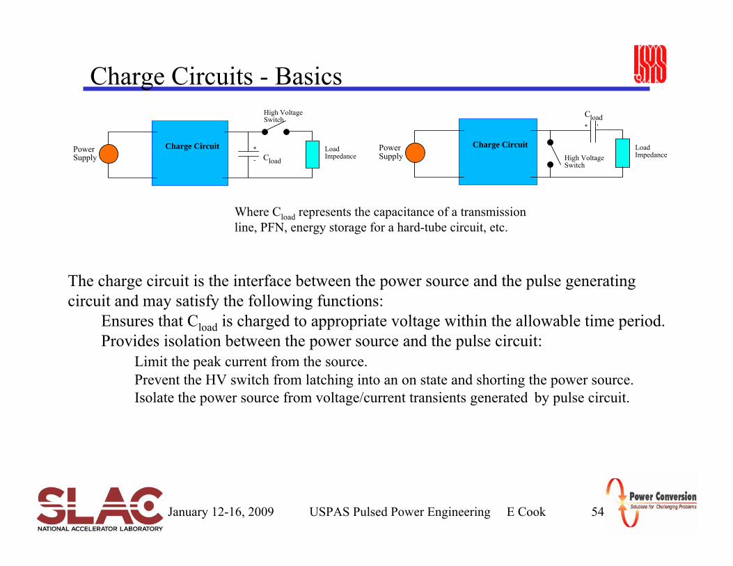
Charge Circuits - Basics
Charge Circuit
High Voltage Switch
Load Impedance
+
-
Power Supply Cload
Where Cload represents the capacitance of a transmission line, PFN, energy storage for a hard-tube circuit, etc.
The charge circuit is the interface between the power source and the pulse generating circuit and may satisfy the following functions:
Ensures that Cload is charged to appropriate voltage within the allowable time period.Provides isolation between the power source and the pulse circuit:
Limit the peak current from the source.Prevent the HV switch from latching into an on state and shorting the power source.Isolate the power source from voltage/current transients generated by pulse circuit.
Charge Circuit High Voltage Switch
Load Impedance
+ -
Power Supply
Cload
January 12-16, 2009 USPAS Pulsed Power Engineering TTU-PPSC 55
AC Power Rectification
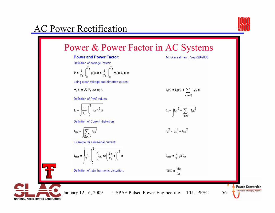
January 12-16, 2009 USPAS Pulsed Power Engineering TTU-PPSC 56
AC Power Rectification
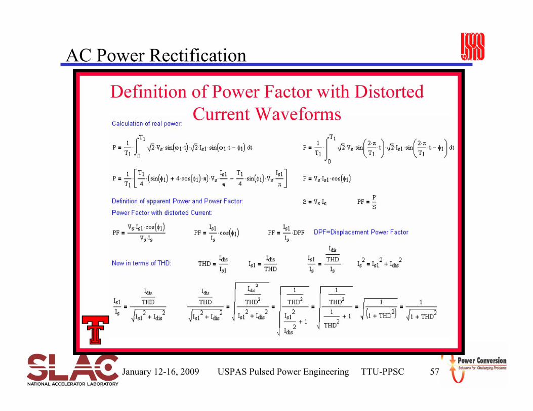
January 12-16, 2009 USPAS Pulsed Power Engineering TTU-PPSC 57
AC Power Rectification
January 12-16, 2009 USPAS Pulsed Power Engineering TTU-PPSC 58
AC Power Rectification

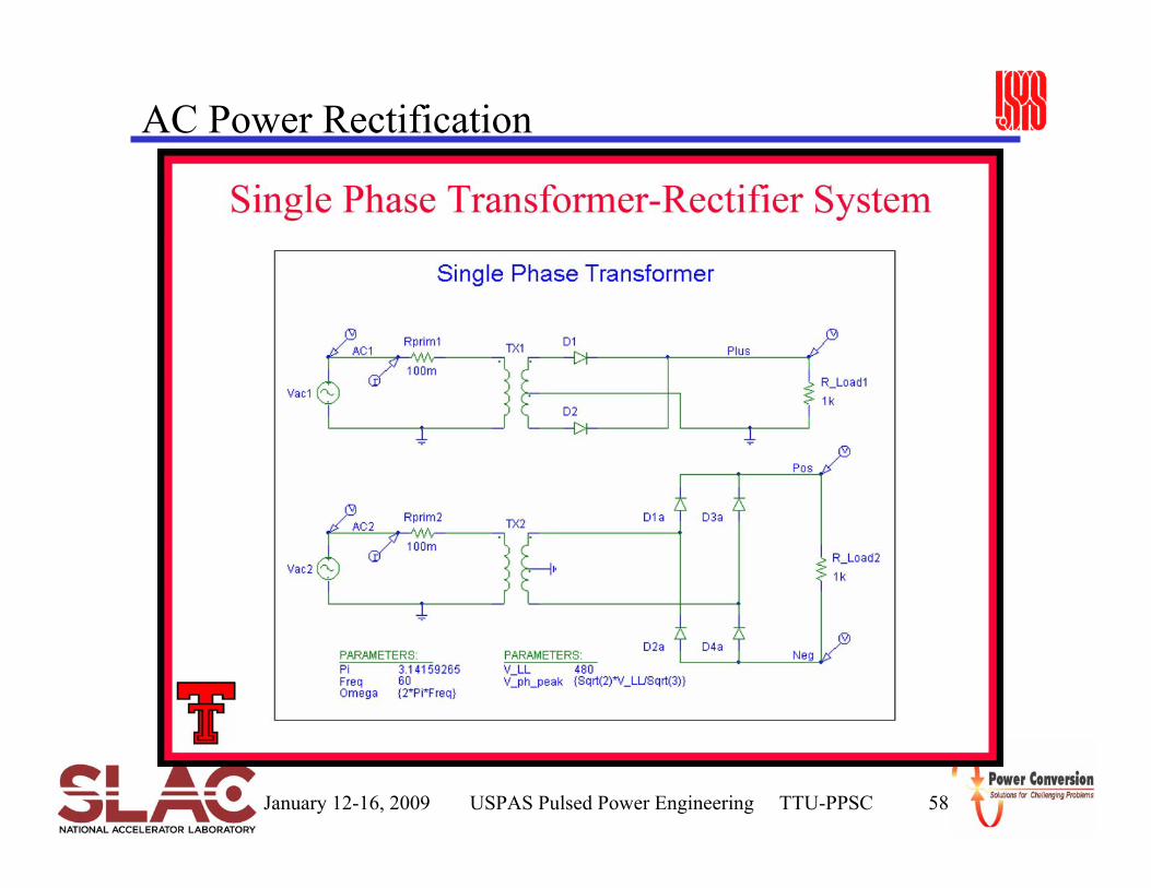
January 12-16, 2009 USPAS Pulsed Power Engineering TTU-PPSC 59
AC Power Rectification
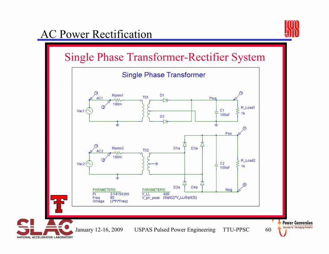
January 12-16, 2009 USPAS Pulsed Power Engineering TTU-PPSC 60
AC Power Rectification

January 12-16, 2009 USPAS Pulsed Power Engineering TTU-PPSC 61
AC Power Rectification
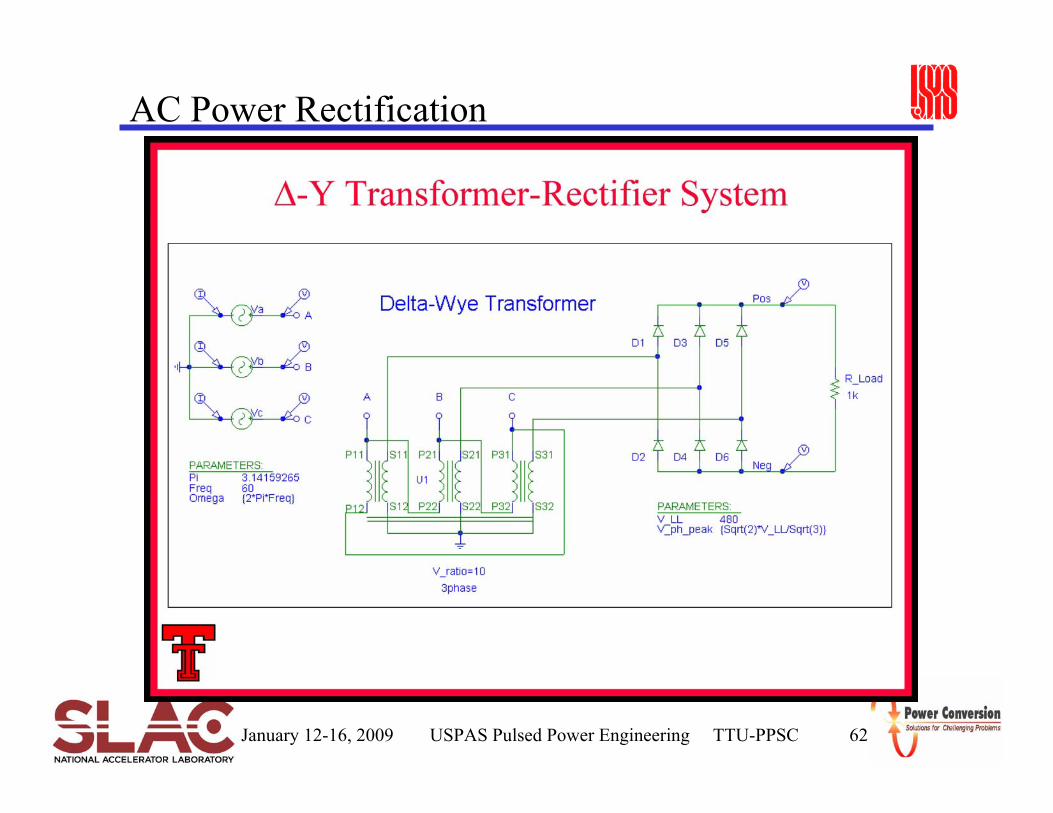
January 12-16, 2009 USPAS Pulsed Power Engineering TTU-PPSC 62
AC Power Rectification
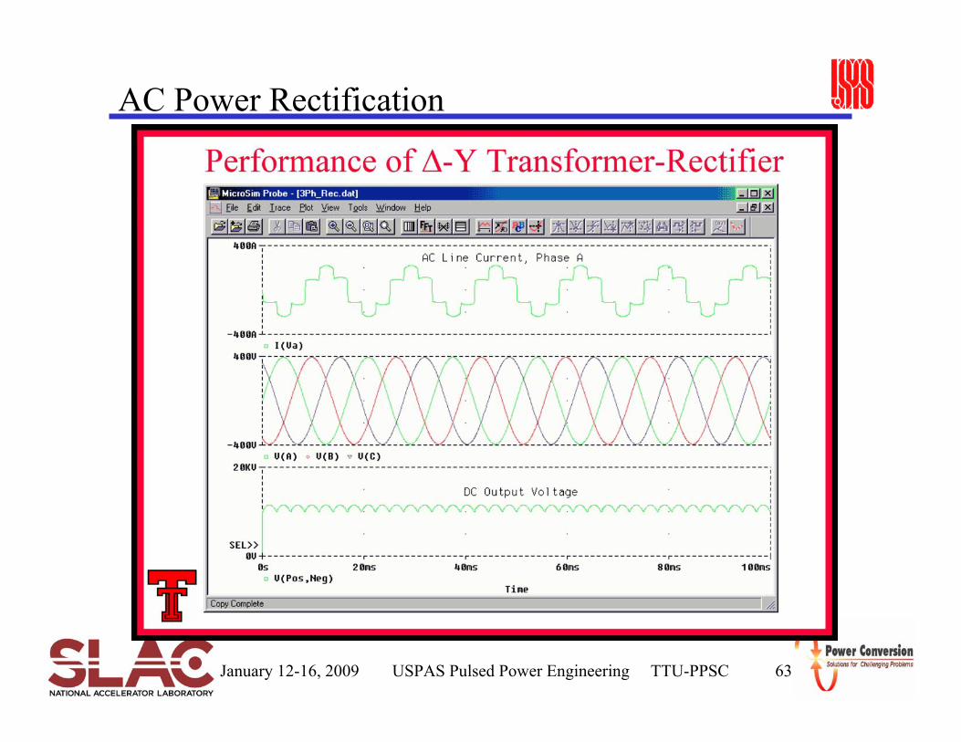
January 12-16, 2009 USPAS Pulsed Power Engineering TTU-PPSC 63
AC Power Rectification

January 12-16, 2009 USPAS Pulsed Power Engineering TTU-PPSC 64
AC Power Rectification
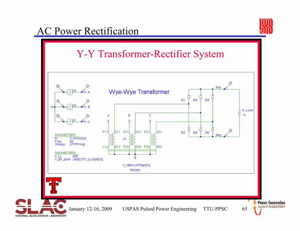
January 12-16, 2009 USPAS Pulsed Power Engineering TTU-PPSC 65
AC Power Rectification
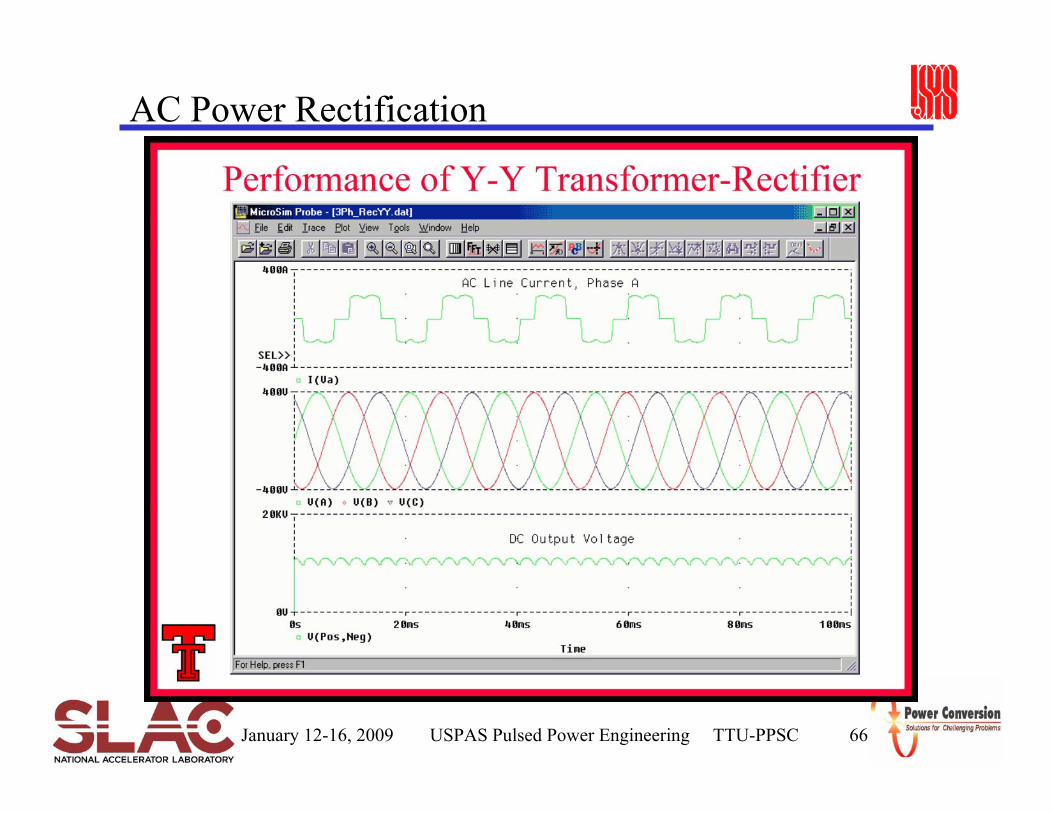
January 12-16, 2009 USPAS Pulsed Power Engineering TTU-PPSC 66
AC Power Rectification
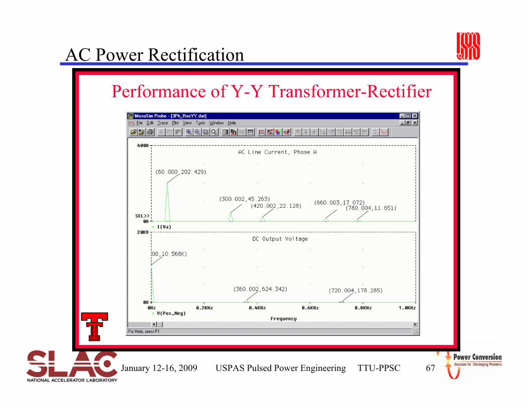
January 12-16, 2009 USPAS Pulsed Power Engineering TTU-PPSC 67
AC Power Rectification
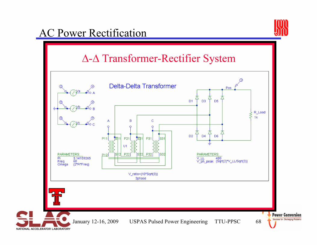
January 12-16, 2009 USPAS Pulsed Power Engineering TTU-PPSC 68
AC Power Rectification
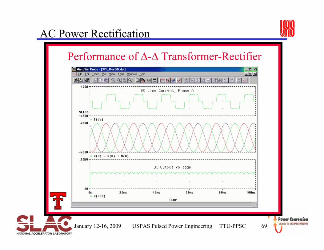
January 12-16, 2009 USPAS Pulsed Power Engineering TTU-PPSC 69
AC Power Rectification

January 12-16, 2009 USPAS Pulsed Power Engineering TTU-PPSC 70
AC Power Rectification
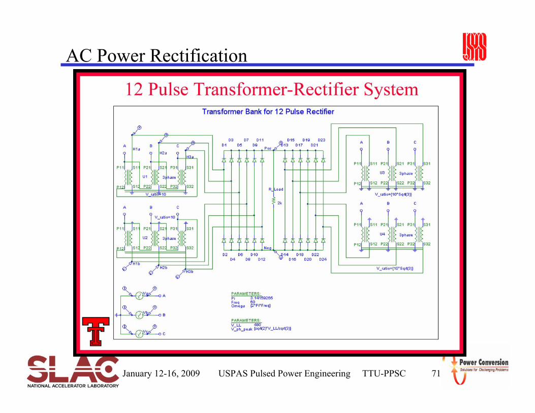
January 12-16, 2009 USPAS Pulsed Power Engineering TTU-PPSC 71
AC Power Rectification
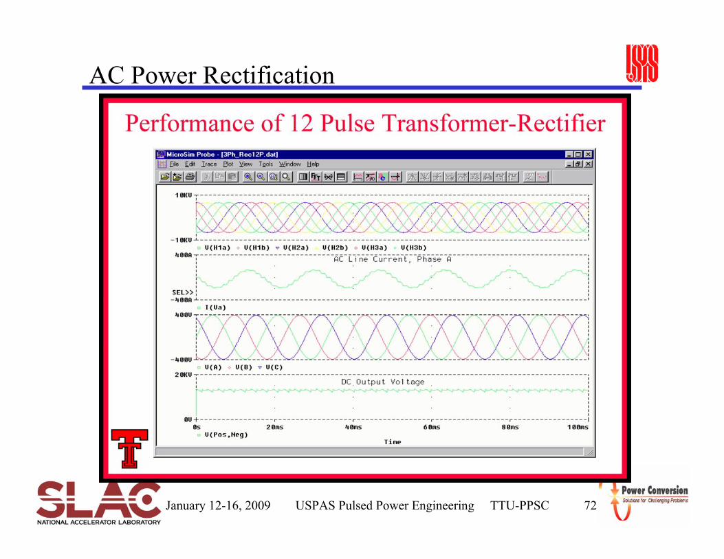
January 12-16, 2009 USPAS Pulsed Power Engineering TTU-PPSC 72
AC Power Rectification

January 12-16, 2009 USPAS Pulsed Power Engineering TTU-PPSC 73
AC Power Rectification
January 12-16, 2009 USPAS Pulsed Power Engineering C Burkhart 74
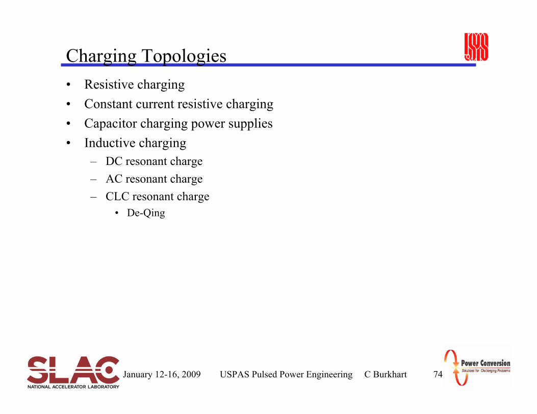
Charging Topologies• Resistive charging• Constant current resistive charging• Capacitor charging power supplies• Inductive charging
– DC resonant charge– AC resonant charge– CLC resonant charge
• De-Qing
January 12-16, 2009 USPAS Pulsed Power Engineering E Cook 75
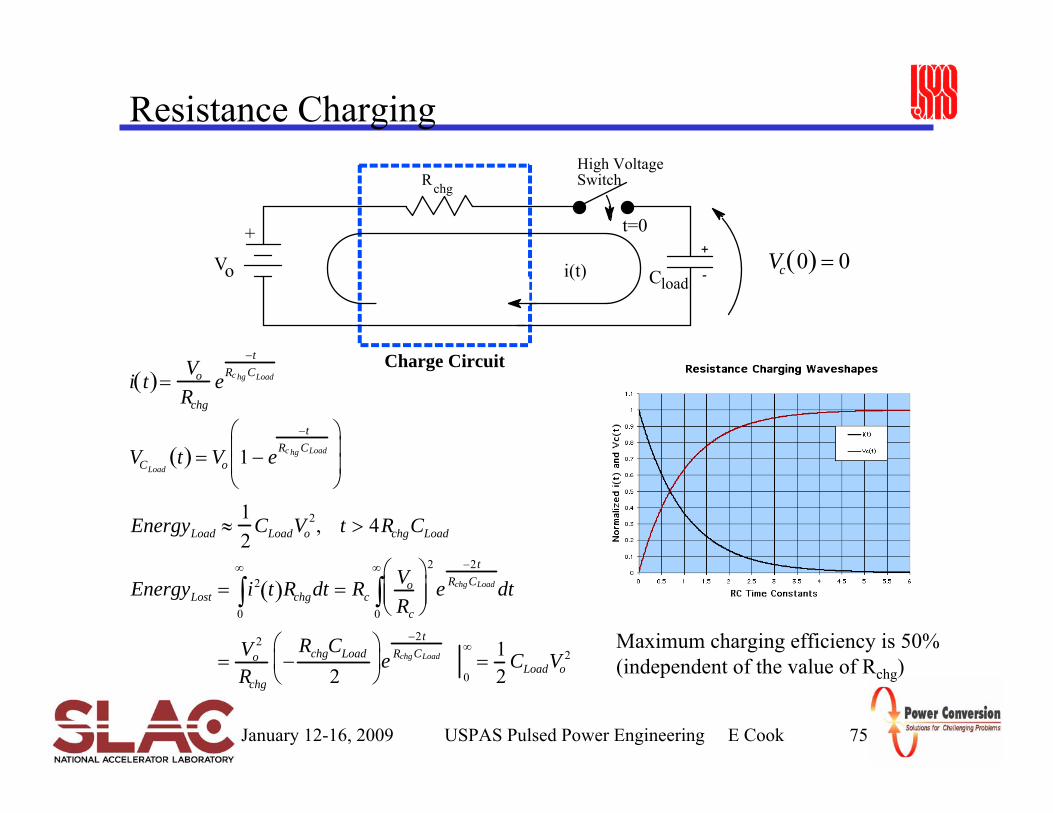
Resistance Charging
Charge Circuit
+
-Cload
+
Rchg
i(t)
High Voltage Switch
t=0
Vo Vc 0( ) = 0
i t( )=Vo
Rchg
e−t
Rc hg CLoad
VCLoadt( ) = Vo 1 − e
−tRc hg CLoad
⎛
⎝
⎜ ⎜
⎞
⎠
⎟ ⎟
EnergyLoad ≈12
CLoadVo2, t > 4RchgCLoad
EnergyLost = i2
0
∞
∫ t( )Rchgdt = RcVo
Rc
⎛
⎝ ⎜ ⎜
⎞
⎠ ⎟ ⎟
2
e−2t
Rchg CLoad
0
∞
∫ dt
= Vo2
Rchg
−RchgCLoad
2⎛
⎝ ⎜
⎞
⎠ ⎟ e
−2tRchg CLoad
0
∞= 1
2CLoadVo
2Maximum charging efficiency is 50% (independent of the value of Rchg)
January 12-16, 2009 USPAS Pulsed Power Engineering E Cook 76
Resistance Charging• Advantages
– Inexpensive– Simple– Allows use of low average power, power supply– May eliminate the need for a high voltage switch– Provides excellent isolation– Stable and repeatable– Charge accuracy is determined by regulation of power supply
• Disadvantages– Inefficient– Slow for high energy transfers– Requires resistor rated for full charge voltage and, depending on the
charge time and energy transferred, a high joule/pulse or average power rating
January 12-16, 2009 USPAS Pulsed Power Engineering Cook/Burkhart 77
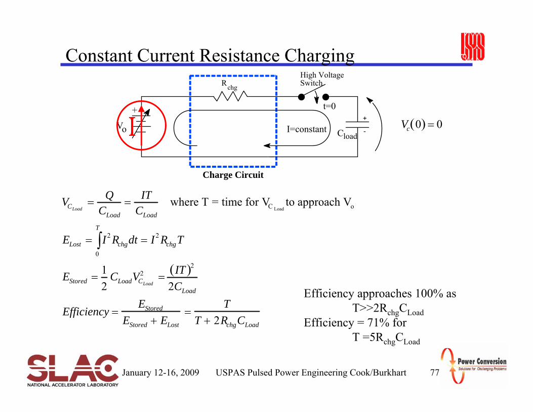
Constant Current Resistance Charging
Charge Circuit
+
-Cload
+
Rchg
I=constant
High Voltage Switch
t=0
Vo Vc 0( ) = 0
VCLoad= Q
CLoad
= ITCLoad
where T = time for VC Loadto approach Vo
ELost = I2
0
T
∫ Rchgdt = I2 RchgT
EStored = 12
CLoadVCLoad
2 = IT( )2
2CLoad
Efficiency =EStored
EStored + ELost
=T
T + 2RchgCLoad
Efficiency approaches 100% as T>>2RchgCLoad
Efficiency = 71% for T =5RchgCLoad
January 12-16, 2009 USPAS Pulsed Power Engineering E Cook 78
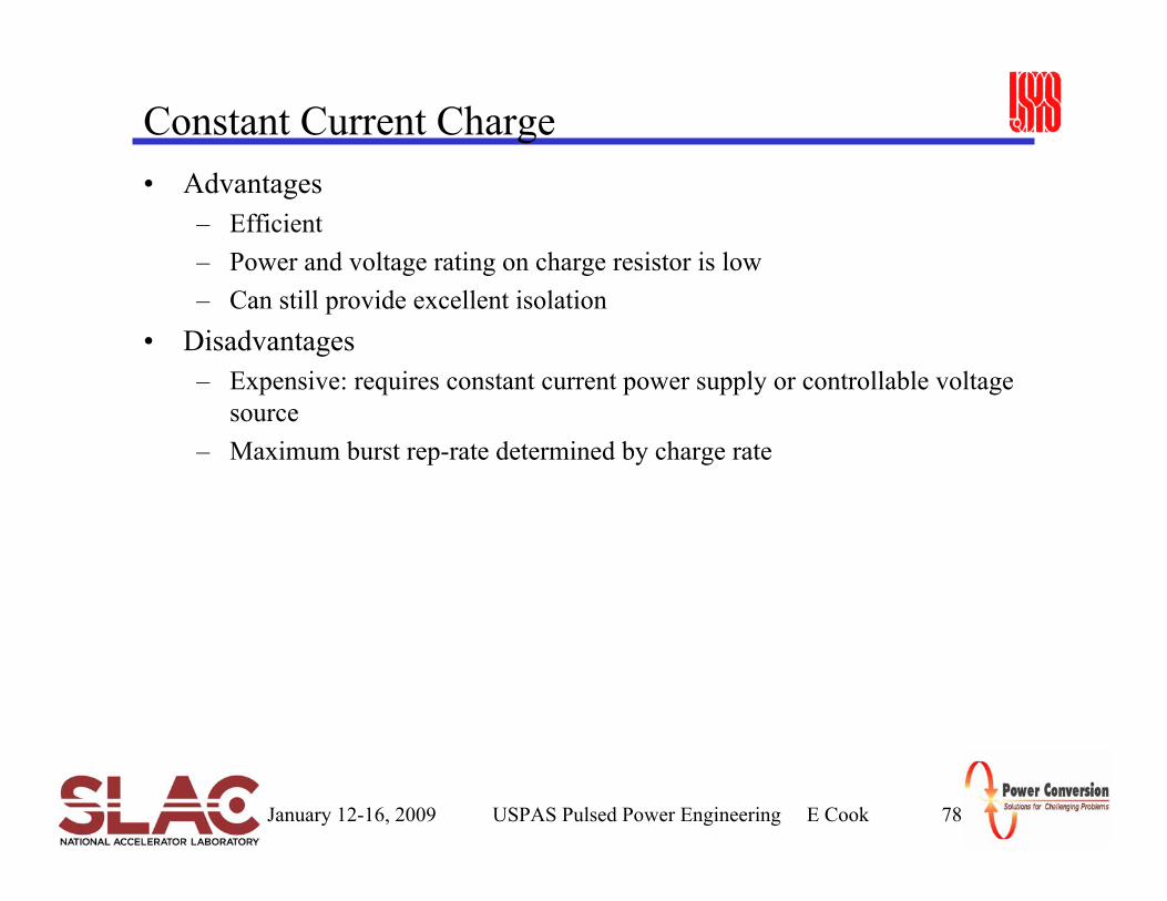
Constant Current Charge• Advantages
– Efficient– Power and voltage rating on charge resistor is low– Can still provide excellent isolation
• Disadvantages– Expensive: requires constant current power supply or controllable voltage
source– Maximum burst rep-rate determined by charge rate
January 12-16, 2009 USPAS Pulsed Power Engineering E Cook 79
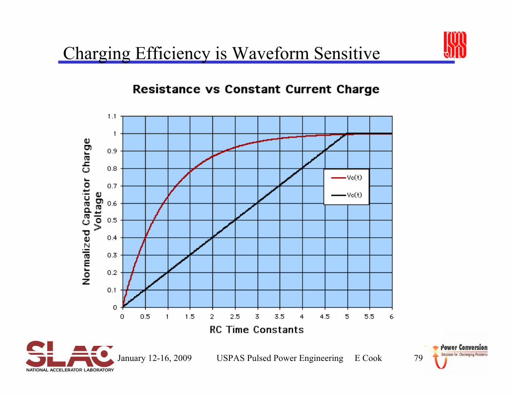
Charging Efficiency is Waveform Sensitive
January 12-16, 2009 USPAS Pulsed Power Engineering E Cook 80
Capacitor Charging Power Supplies
• Positive attributes– Efficient (>85%)– Low stored energy– Stable and accurate (linear to ~1% and with 1% accuracy)– Can be operated from DC output to kHz repetition rates– Compact (high energy density)– Good repeatability (available to <0.1% at rep rates)– Output voltage ranges up to 10’s of kV and controllable from 0-100% at
rated output voltage– Charge rate usually specified at Joules/sec– Internally protected against open circuits, short circuits, overloads and
arcs– Locally or Remotely controllable
Constant current power supply
January 12-16, 2009 USPAS Pulsed Power Engineering E Cook 81
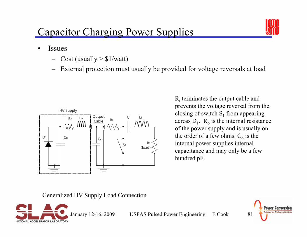
Capacitor Charging Power Supplies• Issues
– Cost (usually > $1/watt)– External protection must usually be provided for voltage reversals at load
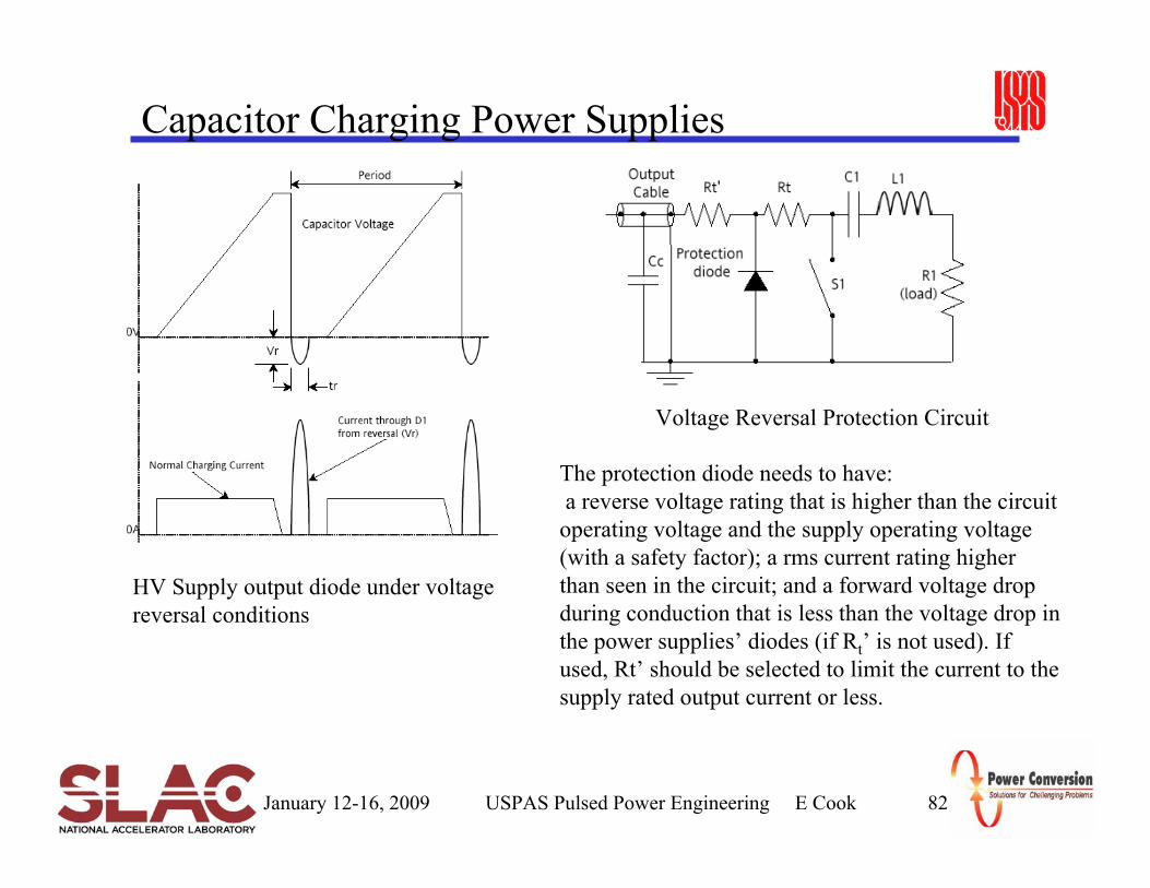
Generalized HV Supply Load Connection
Rt terminates the output cable and prevents the voltage reversal from the closing of switch S1 from appearing across D1. Ro is the internal resistance of the power supply and is usually on the order of a few ohms. Co is the internal power supplies internal capacitance and may only be a few hundred pF.
January 12-16, 2009 USPAS Pulsed Power Engineering E Cook 82
Capacitor Charging Power Supplies
Voltage Reversal Protection Circuit
HV Supply output diode under voltage reversal conditions
The protection diode needs to have:a reverse voltage rating that is higher than the circuit
operating voltage and the supply operating voltage (with a safety factor); a rms current rating higher than seen in the circuit; and a forward voltage drop during conduction that is less than the voltage drop in the power supplies’ diodes (if Rt’ is not used). If used, Rt’ should be selected to limit the current to the supply rated output current or less.
January 12-16, 2009 USPAS Pulsed Power Engineering E Cook 83
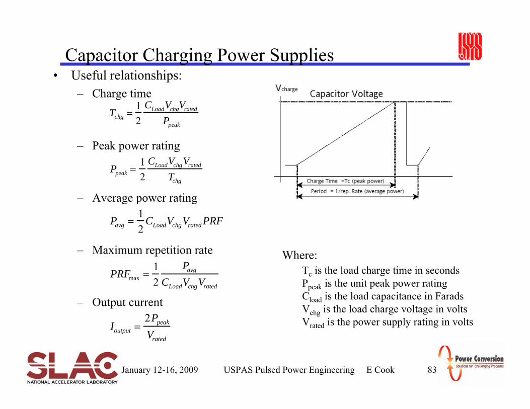
Capacitor Charging Power Supplies• Useful relationships:
– Charge time
– Peak power rating
– Average power rating
– Maximum repetition rate
– Output current
Tchg =12
CLoadVchgVrated
Ppeak
Ppeak =12
CLoadVchgVrated
Tchg
Pavg =12
CLoadVchgVrated PRF
PRFmax =12
Pavg
CLoadVchgVrated
Where:Tc is the load charge time in secondsPpeak is the unit peak power rating Cload is the load capacitance in FaradsVchg is the load charge voltage in voltsVrated is the power supply rating in voltsIoutput =
2Ppeak
Vrated
January 12-16, 2009 USPAS Pulsed Power Engineering C Burkhart 84
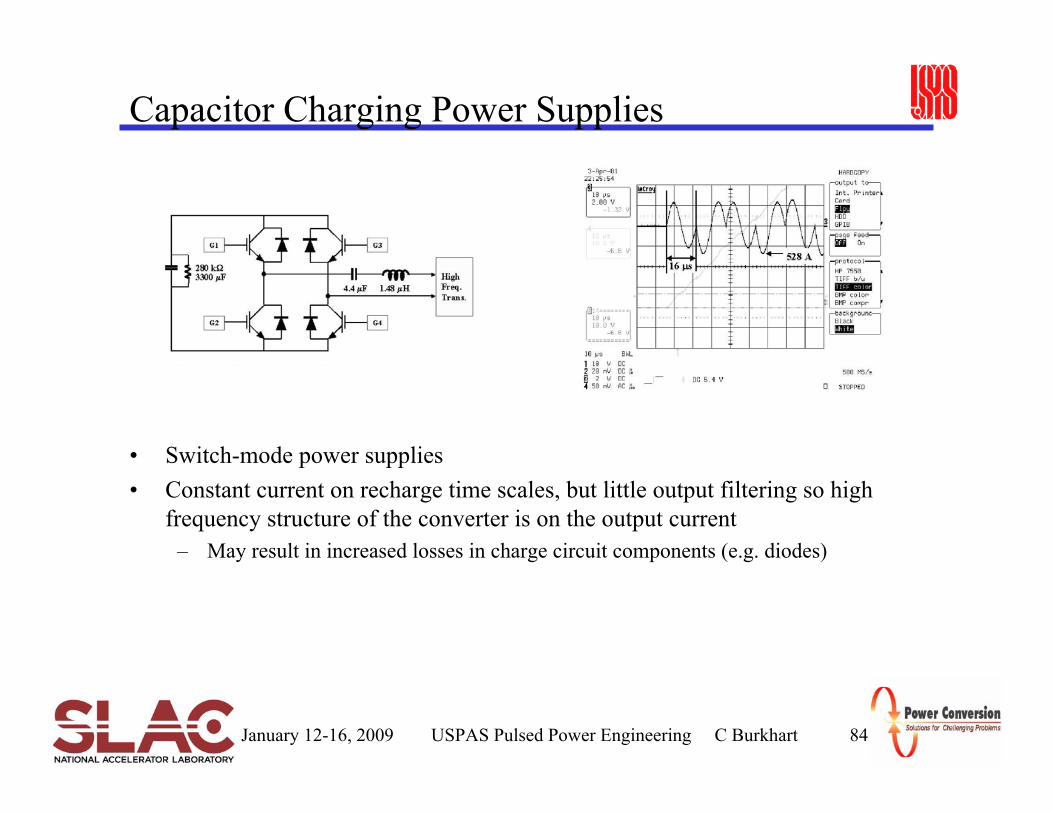
Capacitor Charging Power Supplies
• Switch-mode power supplies• Constant current on recharge time scales, but little output filtering so high
frequency structure of the converter is on the output current– May result in increased losses in charge circuit components (e.g. diodes)
January 12-16, 2009 USPAS Pulsed Power Engineering E Cook 85
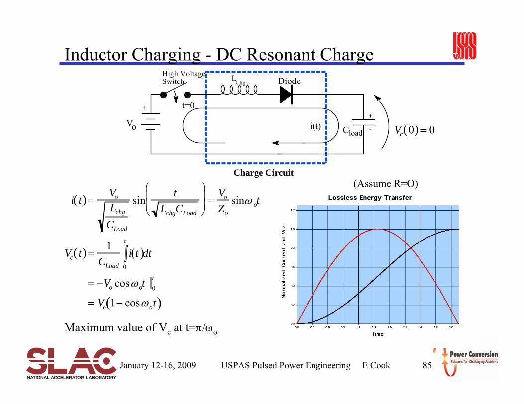
Inductor Charging - DC Resonant ChargeL
Chg
Charge Circuit
+
-Cload
+
i(t)
High Voltage Switch
t=0
Vo
Diode
Vc 0( ) = 0
(Assume R=O)i t( )=
Vo
Lchg
CLoad
sint
LchgCLoad
⎛
⎝ ⎜ ⎜
⎞
⎠ ⎟ ⎟ =
Vo
Zo
sinω ot
Vc t( )=1
CLoad
i t( )0
t
∫ dt
= −Vo cosωot 0t
= Vo 1− cosωot( )
Maximum value of Vc at t=π/ωo
January 12-16, 2009 USPAS Pulsed Power Engineering E Cook 86
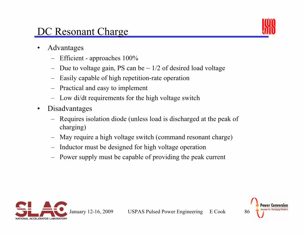
DC Resonant Charge• Advantages
– Efficient - approaches 100%– Due to voltage gain, PS can be ~ 1/2 of desired load voltage– Easily capable of high repetition-rate operation– Practical and easy to implement– Low di/dt requirements for the high voltage switch
• Disadvantages– Requires isolation diode (unless load is discharged at the peak of
charging)– May require a high voltage switch (command resonant charge)– Inductor must be designed for high voltage operation– Power supply must be capable of providing the peak current
January 12-16, 2009 USPAS Pulsed Power Engineering E Cook 87
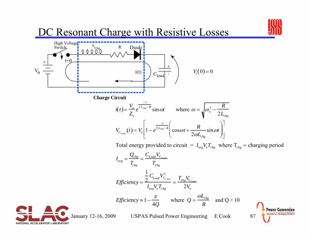
DC Resonant Charge with Resistive LossesL
Chg
Charge Circuit
+
-Cload
+
i(t)
High Voltage Switch
t=0
Vo
R Diode
i t( )=Vo
Zo
e− t
2 Lchg / R sinωt where ω = ωo2 −
R2Lchg
VCLoadt( ) = Vo 1 − e
−t2 Lchg / R cosωt + R
2ωLchg
sinωt⎛
⎝ ⎜ ⎜
⎞
⎠ ⎟ ⎟
⎡
⎣ ⎢ ⎢
⎤
⎦ ⎥ ⎥
Total energy provided to circuit = IavgVoTchg where Tchg = charging period
Iavg =Qchg
Tchg
=CLoadVC Load
Tchg
Efficiency =
12
CLoadVCLoad
2
IavgVoTchg
=TchgVCLoad
2Vo
Efficiency ≈1 −π4Q
where Q =ωLchg
Rand Q > 10
Vc 0( ) = 0
January 12-16, 2009 USPAS Pulsed Power Engineering E Cook 88
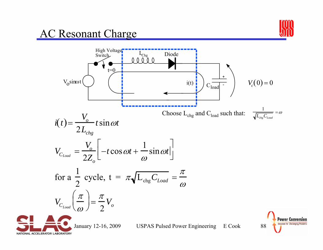
AC Resonant Charge
+
-Cloadi(t)
High Voltage Switch
t=0
Vosinωt
DiodeLChg
Vc 0( ) = 0
Choose Lchg and Cload such that:1
LchgCLoad
=ω
i t( )=Vo
2Lchg
t sinωt
VCLoad=
Vo
2Zo
−t cosωt +1ω
sinωt⎡ ⎣ ⎢
⎤ ⎦ ⎥
for a 12
cycle, t = π LchgCLoad =πω
VCLoad
πω
⎛ ⎝ ⎜
⎞ ⎠ ⎟ =
π2
Vo
January 12-16, 2009 USPAS Pulsed Power Engineering E Cook 89
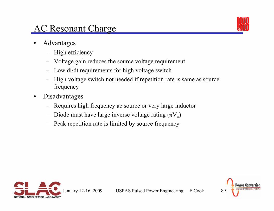
AC Resonant Charge• Advantages
– High efficiency– Voltage gain reduces the source voltage requirement– Low di/dt requirements for high voltage switch– High voltage switch not needed if repetition rate is same as source
frequency• Disadvantages
– Requires high frequency ac source or very large inductor– Diode must have large inverse voltage rating (πVo)– Peak repetition rate is limited by source frequency
January 12-16, 2009 USPAS Pulsed Power Engineering E Cook 90
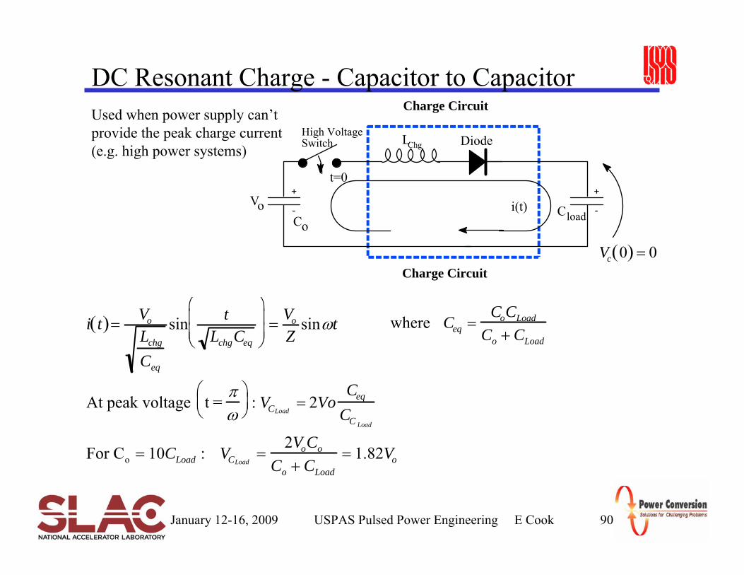
DC Resonant Charge - Capacitor to CapacitorCharge Circuit
Charge Circuit
+
-Cloadi(t)
High Voltage Switch
t=0
Vo
Diode
+
-Co
LChg
Vc 0( ) = 0
Used when power supply can’t provide the peak charge current (e.g. high power systems)
i t( )= Vo
Lchg
Ceq
sin tLchgCeq
⎛
⎝ ⎜ ⎜
⎞
⎠ ⎟ ⎟ =
Vo
Zsinωt
At peak voltage t =πω
⎛ ⎝ ⎜
⎞ ⎠ ⎟ : VCLoad
= 2VoCeq
CC Load
For Co = 10CLoad : VCLoad=
2VoCo
Co + CLoad
= 1.82Vo
where Ceq =CoCLoad
Co + CLoad
January 12-16, 2009 USPAS Pulsed Power Engineering E Cook 91
DC Resonant Charge - Capacitor to Capacitor• Advantages
– Efficient– Voltage gain reduced the PS voltage requirement– Easily capable of high repetition rate operation– Can operate asynchronously– Power supply isn’t required to provide large charge current when system
is operating at low duty factor– Low di/dt requirements on high voltage switch
• Disadvantages– Requires a large DC capacitor bank– DC capacitor bank needs to be fully recharged between pulses to ensure
voltage regulation at the load, unless alternative regulation techniques are employed
January 12-16, 2009 USPAS Pulsed Power Engineering E Cook 92
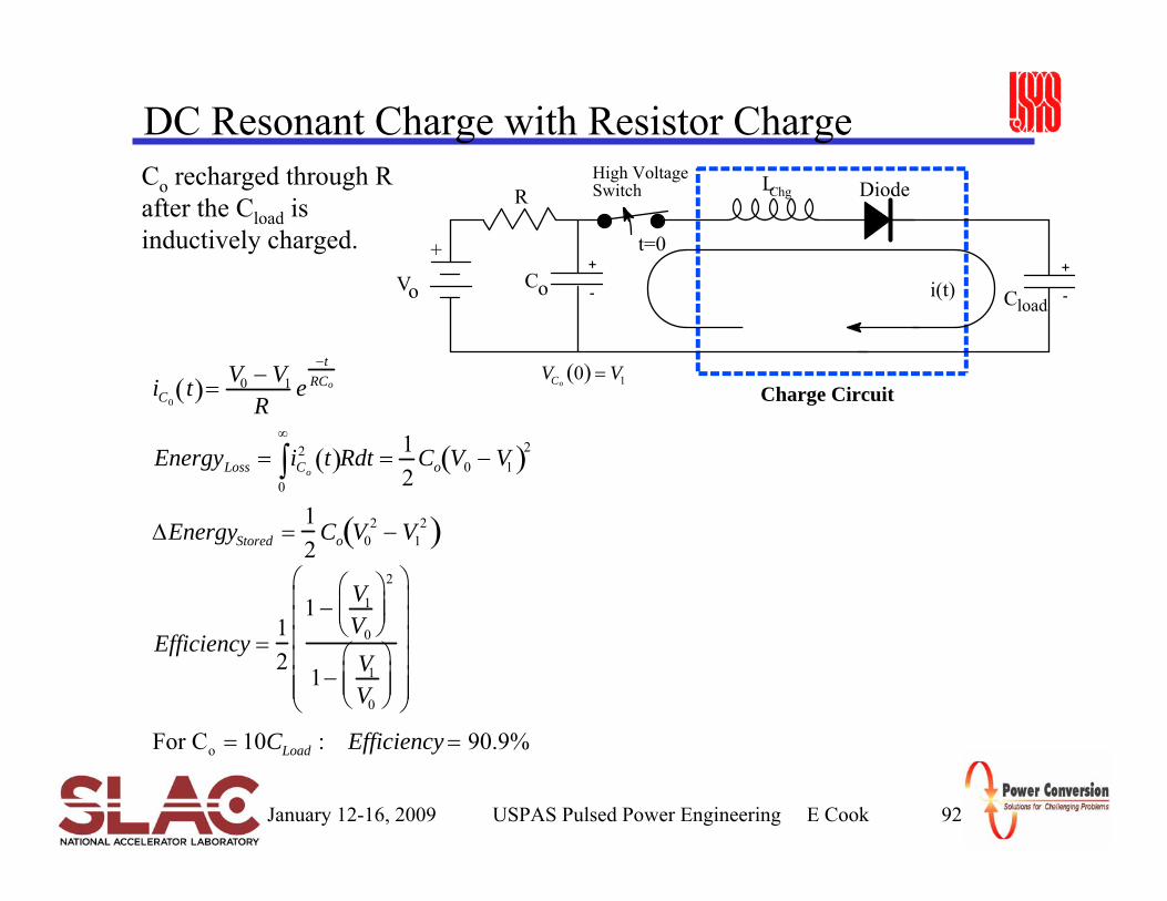
DC Resonant Charge with Resistor Charge
VCo0( ) = V1iC0
t( )= V0 − V1
Re
−tRCo
EnergyLoss = iCo
2
0
∞
∫ t( )Rdt = 12
Co V0 − V1( )2
ΔEnergyStored =12
Co V02 − V1
2( )
Efficiency =12
1 − V1
V0
⎛
⎝ ⎜ ⎜
⎞
⎠ ⎟ ⎟
2
1− V1
V0
⎛
⎝ ⎜ ⎜
⎞
⎠ ⎟ ⎟
⎛
⎝
⎜ ⎜ ⎜ ⎜ ⎜ ⎜
⎞
⎠
⎟ ⎟ ⎟ ⎟ ⎟ ⎟
For Co = 10CLoad : Efficiency = 90.9%
Co recharged through R after the Cload is inductively charged.
Charge Circuit
+
-Cload
+
i(t)
High Voltage Switch
t=0
Vo
Diode
+
-Co
R LChg
January 12-16, 2009 USPAS Pulsed Power Engineering E Cook 93
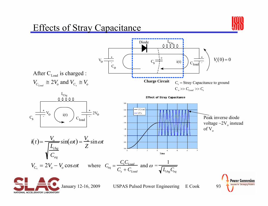
Effects of Stray Capacitance
Charge Circuit
Vo+
-
+
-Cloadi(t)
Diode
CoCs
+
LChg
Cs = Stray Capacitance to groundCo >> CLoad >> Cs
After CLoad is charged :VCLoad
≅ 2Vo and VCs≅ Vo
Vc 0( ) = 0
Vo+
-
+
-Cloadi(t)Cs
2Vo
LChg
where Ceq =CsCLoad
Cs + CLoad
and ω =1
LchgCeq
i t( )= Vo
Lchg
Ceq
sin ωt( ) = Vo
Zsinωt
VCs= 2Vo − Vo cosωt
Peak inverse diode voltage ~2Vo instead of Vo
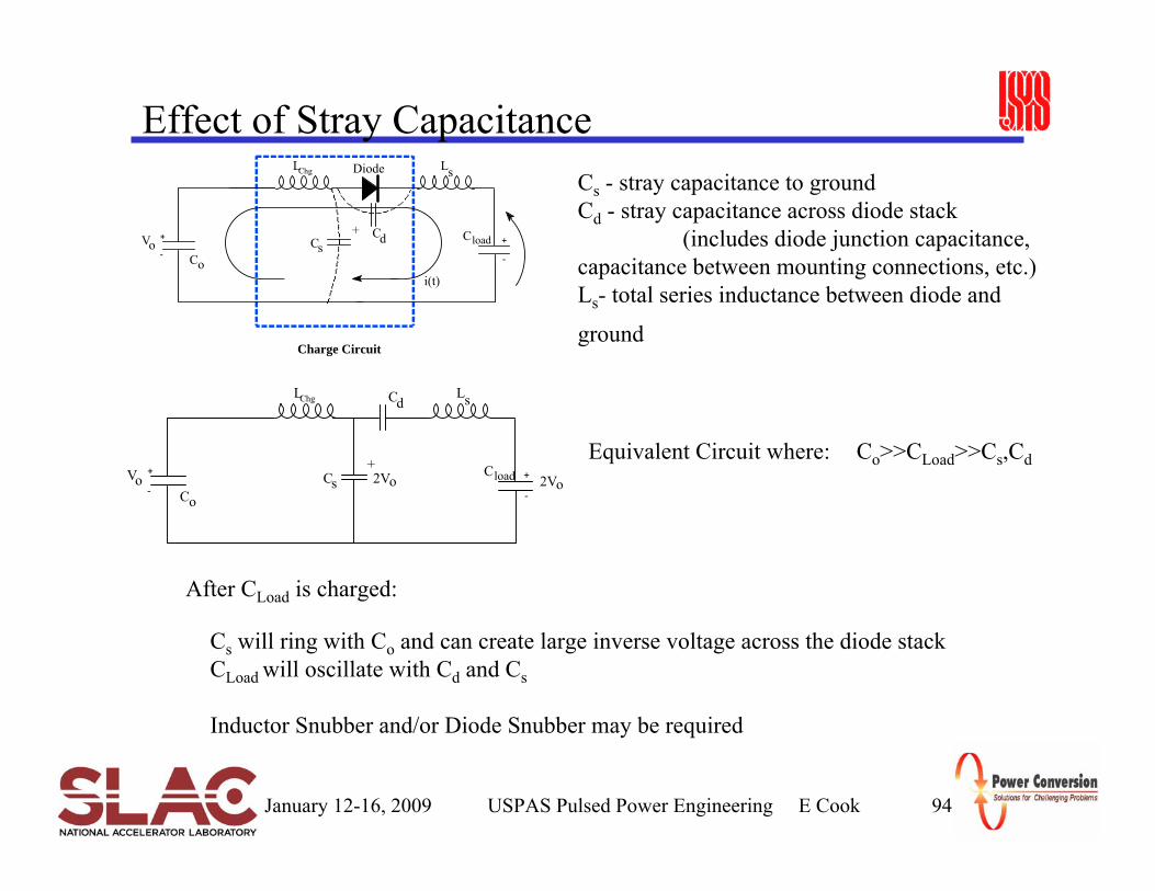
January 12-16, 2009 USPAS Pulsed Power Engineering E Cook 94
Effect of Stray CapacitanceLChg
Charge Circuit
Vo+
-+
-
Cload
i(t)
Diode
Co
Cs+ Cd
Ls Cs - stray capacitance to groundCd - stray capacitance across diode stack
(includes diode junction capacitance, capacitance between mounting connections, etc.)Ls- total series inductance between diode and
ground
LChg
Vo+
-+
-
Cload
Co
Cs+
CdLs
2Vo2Vo
Equivalent Circuit where: Co>>CLoad>>Cs,Cd
After CLoad is charged:
Cs will ring with Co and can create large inverse voltage across the diode stackCLoad will oscillate with Cd and Cs
Inductor Snubber and/or Diode Snubber may be required
January 12-16, 2009 USPAS Pulsed Power Engineering E Cook 95
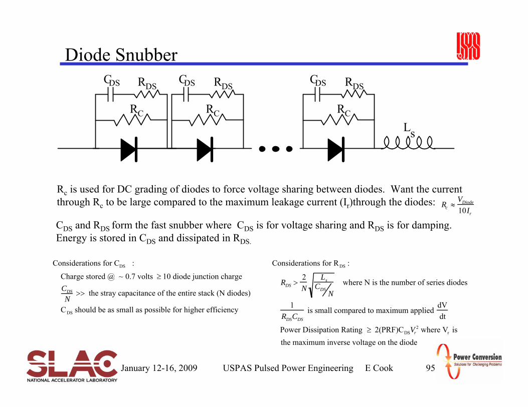
Diode Snubber
RC
RDSCDS
Ls
RC
RDSCDS
RC
RDSCDS
Rc is used for DC grading of diodes to force voltage sharing between diodes. Want the current through Rc to be large compared to the maximum leakage current (Ir)through the diodes: Rc ≈
VDiode
10Ir
CDS and RDS form the fast snubber where CDS is for voltage sharing and RDS is for damping. Energy is stored in CDS and dissipated in RDS.
Considerations for RDS :
RDS >2N
LsCDS
Nwhere N is the number of series diodes
1RDSCDS
is small compared to maximum applied dVdt
Power Dissipation Rating ≥ 2(PRF)CDSVr2 where Vr is
the maximum inverse voltage on the diode
Considerations for CDS :
Charge stored @ ~ 0.7 volts ≥ 10 diode junction chargeCDS
N>> the stray capacitance of the entire stack (N diodes)
CDS should be as small as possible for higher efficiency
January 12-16, 2009 USPAS Pulsed Power Engineering E Cook 96
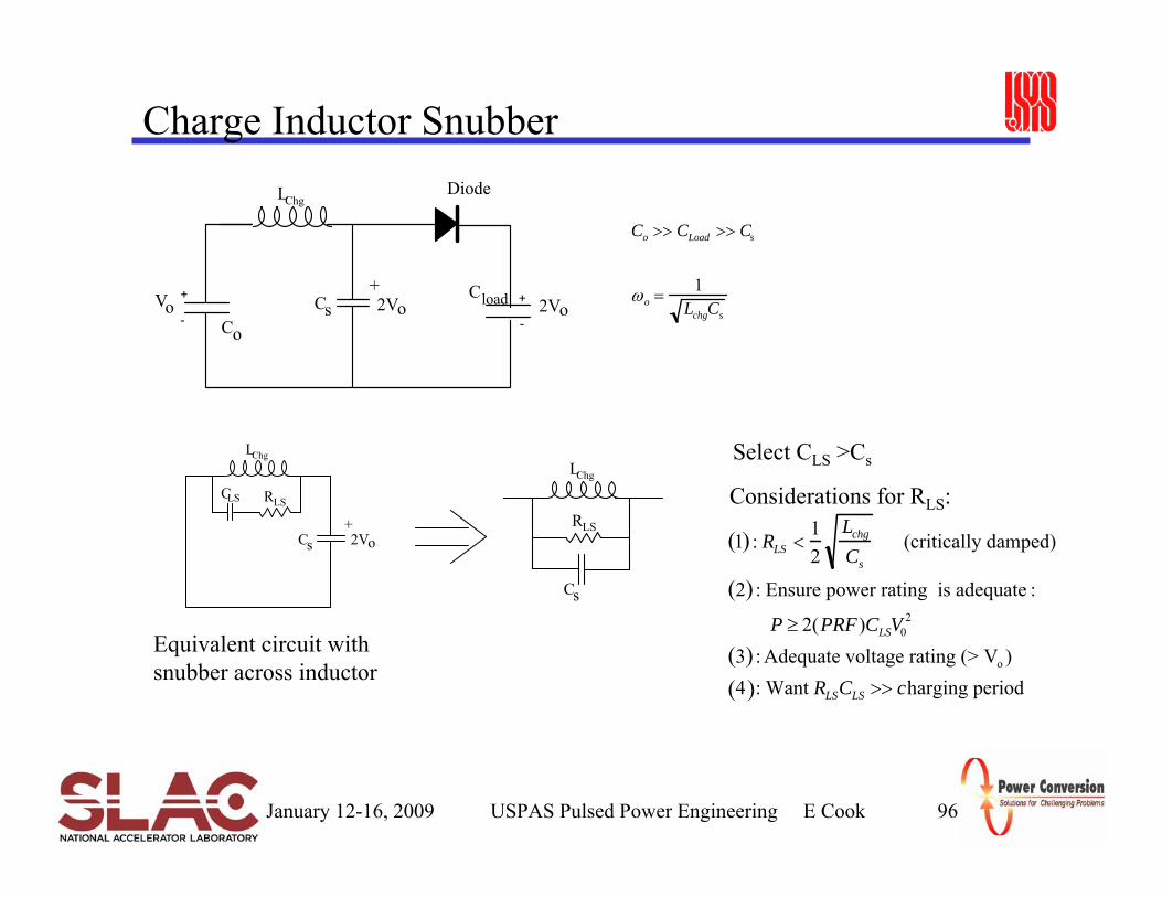
Charge Inductor SnubberLChg
Vo+
-
+
-
Cload 2VoCo
Cs+2Vo
Diode
LChg
Cs+2Vo
RLSCLS
LChg
Cs
RLS
Co >> CLoad >> Cs
ωo = 1LchgCs
Select CLS >Cs
Considerations for RLS:
1( ) : RLS <12
Lchg
Cs
(critically damped)
2( ) : Ensure power rating is adequate :
P ≥ 2(PRF)CLSV02
3( ) : Adequate voltage rating (> Vo )4( ): Want RLSCLS >> charging period
Equivalent circuit with snubber across inductor
January 12-16, 2009 USPAS Pulsed Power Engineering C Burkhart 97
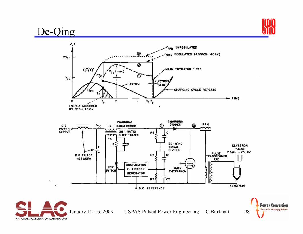
Inductive Charging Voltage Regulation• For klystron phase stability, PFN charge voltage regulation may need
to be ~10 ppm• High power supplies usually do not have precise regulation
– Requires more complicated topologies (over simple rectifier/filter)– Increases cost
• Common approach to regulate PFN charge voltage from unregulated source is de-Qing
– Monitor PFN voltage during charge cycle– When PFN reaches final voltage, shunt energy remaining in charge
inductor to dummy load
January 12-16, 2009 USPAS Pulsed Power Engineering C Burkhart 98
De-Qing
January 12-16, 2009 USPAS Pulsed Power Engineering C Burkhart 99
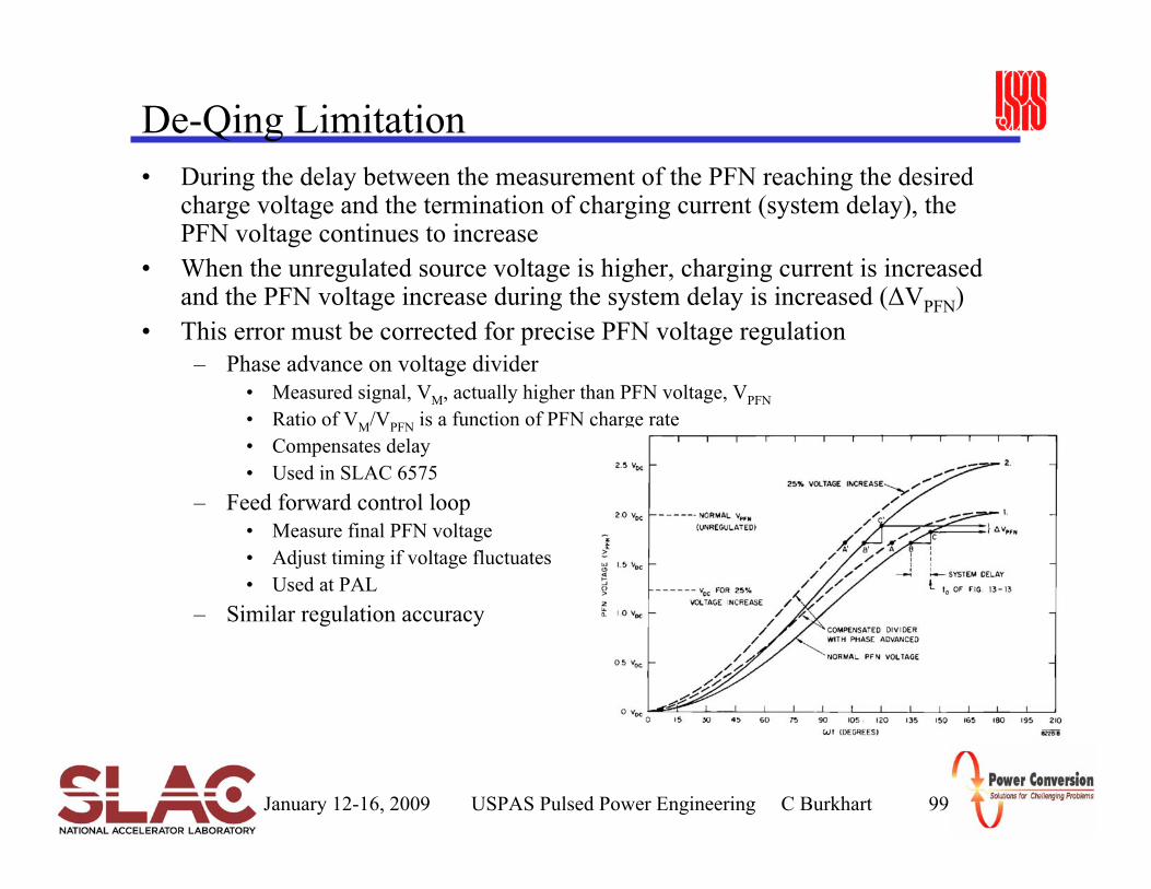
De-Qing Limitation• During the delay between the measurement of the PFN reaching the desired
charge voltage and the termination of charging current (system delay), the PFN voltage continues to increase
• When the unregulated source voltage is higher, charging current is increased and the PFN voltage increase during the system delay is increased (ΔVPFN)
• This error must be corrected for precise PFN voltage regulation– Phase advance on voltage divider
• Measured signal, VM, actually higher than PFN voltage, VPFN• Ratio of VM/VPFN is a function of PFN charge rate• Compensates delay• Used in SLAC 6575
– Feed forward control loop• Measure final PFN voltage• Adjust timing if voltage fluctuates• Used at PAL
– Similar regulation accuracy
January 12-16, 2009 USPAS Pulsed Power Engineering C Burkhart 100
Control System Functions• Control output waveform
– Voltage– Pulse shape– Timing
• Protect system (MPS)– Over voltage– Over current– Heater time-outs– Etc.
• Protect personnel (PPS)– PPS interlocks– Emergency Off– Access interlocks– Energy discharge
• Bleeder resistors across capacitors• Engineered grounds
January 12-16, 2009 USPAS Pulsed Power Engineering C Burkhart 101
Control System Elements• Lab Scale: independent elements
– Charging supply with integrated controls– Trigger generator– Diagnostics
• Oscilloscope• Probes
– Voltage divider– Current transformer
• Installations– Control system interfaces to many operators/users and many other
machines/systems: an integrated control system is required• Periodic evaluation• Configuration control
– Control system may incorporate many components at varying levels• Integrated modulator control (modern trend)• System level (e.g. HLRF)• Facility level (e.g. accelerator)
January 12-16, 2009 USPAS Pulsed Power Engineering C Burkhart 102
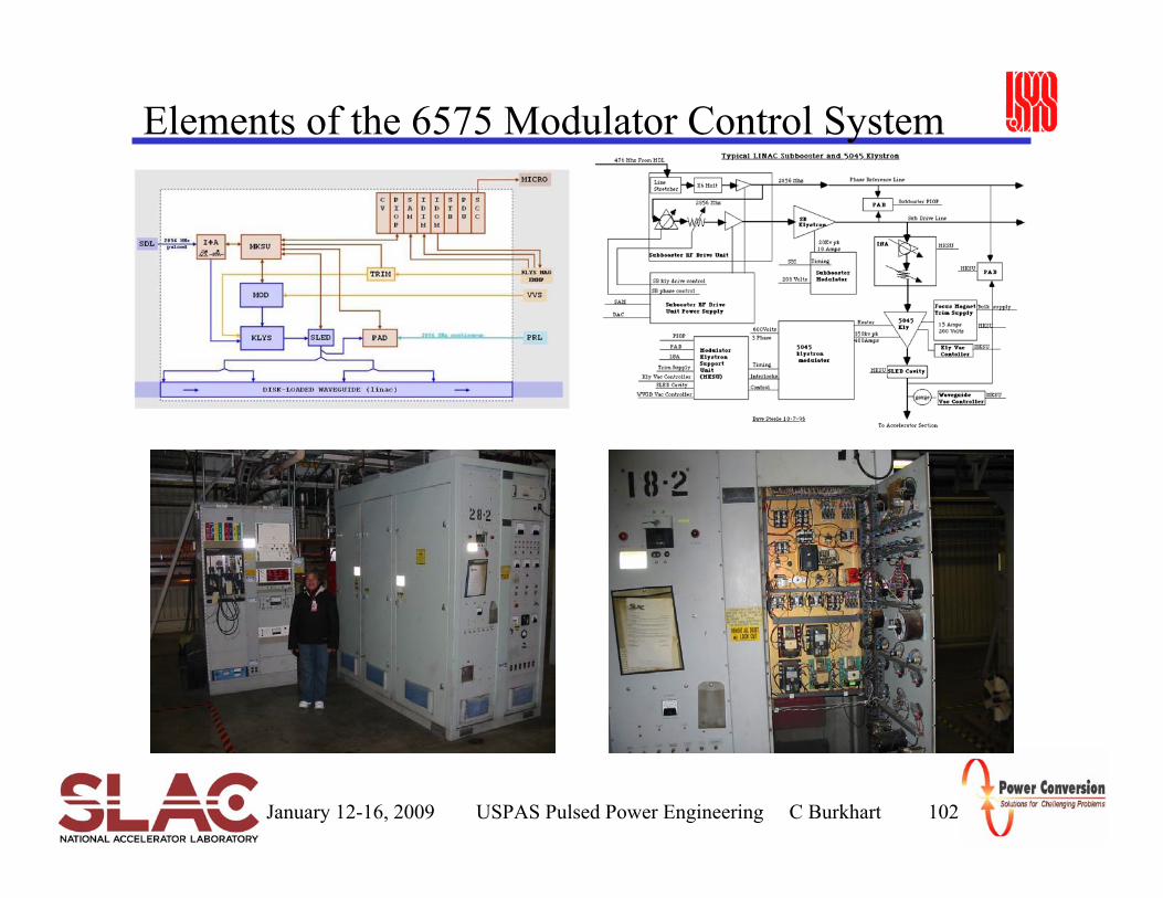
Elements of the 6575 Modulator Control System
January 12-16, 2009 USPAS Pulsed Power Engineering C Burkhart 103
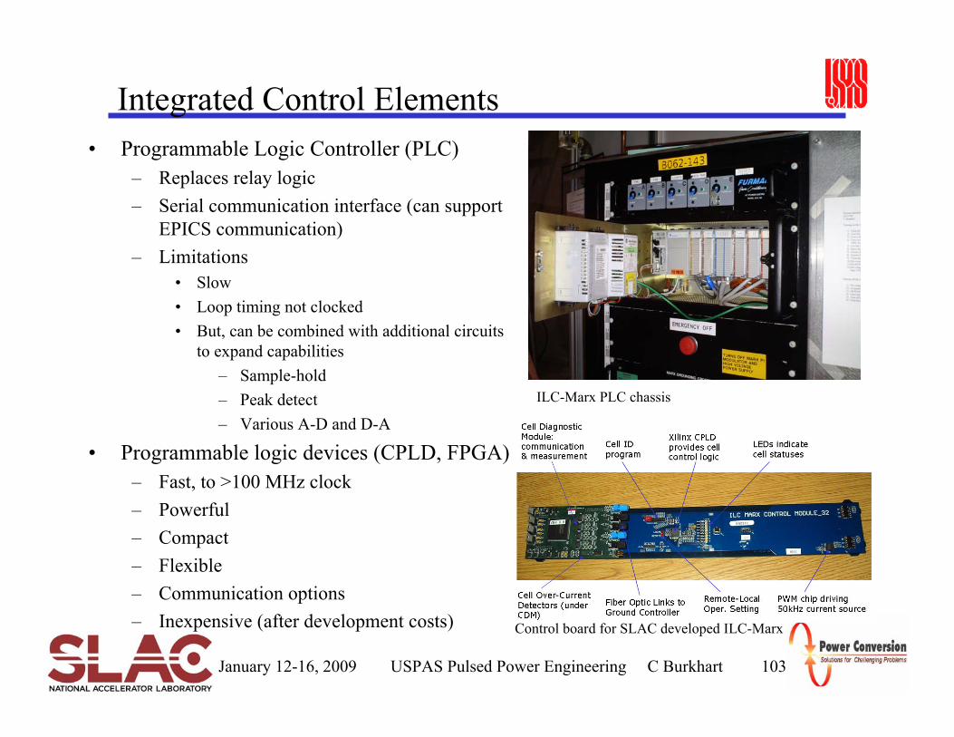
Integrated Control Elements• Programmable Logic Controller (PLC)
– Replaces relay logic– Serial communication interface (can support
EPICS communication)– Limitations
• Slow• Loop timing not clocked• But, can be combined with additional circuits
to expand capabilities– Sample-hold– Peak detect– Various A-D and D-A
• Programmable logic devices (CPLD, FPGA)– Fast, to >100 MHz clock– Powerful– Compact– Flexible – Communication options– Inexpensive (after development costs) Control board for SLAC developed ILC-Marx
ILC-Marx PLC chassis