Power Ampli ers - University of California, Berkeleyrfic.eecs.berkeley.edu/142/pdf/module19.pdf ·...
27
Berkeley Power Amplifiers Prof. Ali M. Niknejad U.C. Berkeley Copyright c 2016 by Ali M. Niknejad April 8, 2016 1 / 27
-
Upload
truongthuy -
Category
Documents
-
view
217 -
download
0
Transcript of Power Ampli ers - University of California, Berkeleyrfic.eecs.berkeley.edu/142/pdf/module19.pdf ·...
Berkeley
Power Amplifiers
Prof. Ali M. Niknejad
U.C. BerkeleyCopyright c© 2016 by Ali M. Niknejad
April 8, 2016
1 / 27
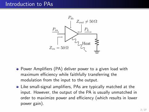
Introduction to PAs
Heat
Pin PL
Pdc
Zin = 50!
Zout != 50!
Power Amplifiers (PA) deliver power to a given load withmaximum efficiency while faithfully transferring themodulation from the input to the output.
Like small-signal amplifiers, PAs are typically matched at theinput. However, the output of the PA is usually unmatched inorder to maximize power and efficiency (which results in lowerpower gain).
2 / 27
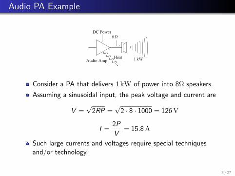
Audio PA Example
Audio Amp
8!
1 kWHeat
DC Power
Consider a PA that delivers 1 kW of power into 8Ω speakers.
Assuming a sinusoidal input, the peak voltage and current are
V =√
2RP =√
2 · 8 · 1000 = 126 V
I =2P
V= 15.8 A
Such large currents and voltages require special techniquesand/or technology.
3 / 27
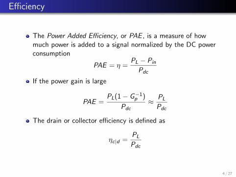
Efficiency
The Power Added Efficiency, or PAE , is a measure of howmuch power is added to a signal normalized by the DC powerconsumption
PAE = η =PL − Pin
Pdc
If the power gain is large
PAE =PL(1− G−1p )
Pdc≈ PL
Pdc
The drain or collector efficiency is defined as
ηc|d =PL
Pdc
4 / 27
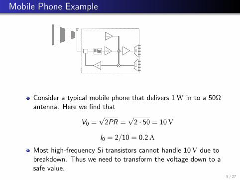
Mobile Phone Example
AD
C
VCO
LNA
DA
C
PA
Consider a typical mobile phone that delivers 1 W in to a 50Ωantenna. Here we find that
V0 =√
2PR =√
2 · 50 = 10 V
I0 = 2/10 = 0.2 A
Most high-frequency Si transistors cannot handle 10 V due tobreakdown. Thus we need to transform the voltage down to asafe value.
5 / 27
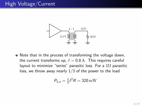
High Voltage/Current
4 : 1
50!
10V
2.5V
Note that in the process of transforming the voltage down,the current transforms up, I = 0.8 A. This requires carefullayout to minimize “series” parasitic loss. For a 1Ω parasiticloss, we throw away nearly 1/3 of the power to the load
PL,s = 12 I
2R = 320 mW
6 / 27
Effect of Loss
If the core amplifier efficiency is say 50%, then this externalloss cuts the efficiency to
Ploss = 320 mW +PL
η= 2.32 W
η =1 W
2.32 W= 43%
If the transformer has 2 dB of insertion loss, then the efficiency(and output power) drops by a factor 0f .63, or η =27%.
7 / 27
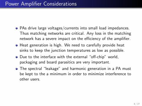
Power Amplifier Considerations
PAs drive large voltages/currents into small load impedances.Thus matching networks are critical. Any loss in the matchingnetwork has a severe impact on the efficiency of the amplifier.
Heat generation is high. We need to carefully provide heatsinks to keep the junction temperatures as low as possible.
Due to the interface with the external “off-chip” world,packaging and board parasitics are very important.
The spectral “leakage” and harmonic generation in a PA mustbe kept to the a minimum in order to minimize interference toother users.
8 / 27
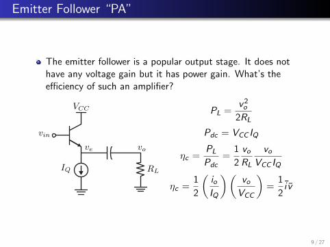
Emitter Follower “PA”
The emitter follower is a popular output stage. It does nothave any voltage gain but it has power gain. What’s theefficiency of such an amplifier?
vin
ve vo
IQ
VCC
RL
PL =v2o
2RL
Pdc = VCC IQ
ηc =PL
Pdc=
1
2
voRL
voVCC IQ
ηc =1
2
(ioIQ
)(voVCC
)=
1
2i v
9 / 27
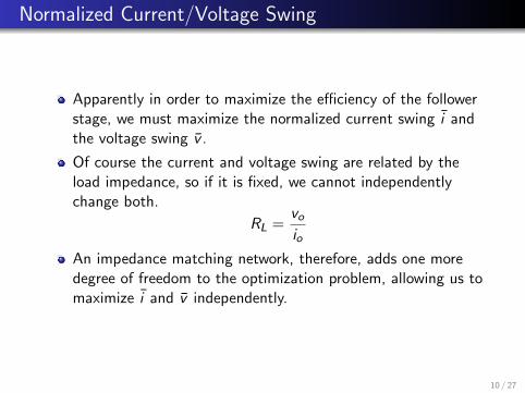
Normalized Current/Voltage Swing
Apparently in order to maximize the efficiency of the followerstage, we must maximize the normalized current swing i andthe voltage swing v .
Of course the current and voltage swing are related by theload impedance, so if it is fixed, we cannot independentlychange both.
RL =voio
An impedance matching network, therefore, adds one moredegree of freedom to the optimization problem, allowing us tomaximize i and v independently.
10 / 27
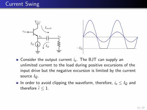
Current Swing
vin
ve vo
IQ
VCC
IQ
Imelt
!IQ
Consider the output current io . The BJT can supply anunlimited current to the load during positive excursions of theinput drive but the negative excursion is limited by the currentsource IQ .
In order to avoid clipping the waveform, therefore, io ≤ IQ andtherefore i ≤ 1.
11 / 27
Voltage Swing
The maximum positive output voltage certainly cannot exceedthe power supply voltage VCC . Also, if the follower transistorremains active during the entire cycle, then the maximumvoltage is set by the input bias level minus VBE .
If the input voltage exceeds the supply, the transistorbase-collector junction forward biases. Under “saturation”,the maximum voltage is therefore given byvomax = VCC − VCE ,sat . In reality, we would never push ourtransistor this hard because it would generate a lot ofdistortion.
Likewise, the minimum voltage occurs when we saturate ourcurrent source, at a value of vomin = VCE ,sat
12 / 27
Voltage Swing (cont)
VCC ! VCE!sat
VCE!sat
VQ,low
VQ,high
VQ,mid
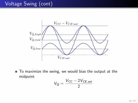
To maximize the swing, we would bias the output at themidpoint
VQ =VCC − 2VCE ,sat
2
13 / 27
Follower Efficiency
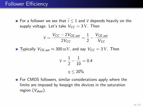
For a follower we see that i ≤ 1 and v depends heavily on thesupply voltage. Let’s take VCC = 3 V. Then
v =VCC − 2VCE ,sat
2VCC=
1
2− VCE ,sat
VCC
Typically VCE ,sat ≈ 300 mV, and say VCC = 3 V. Then
v =1
2− 1
10= 0.4
η ≤ 20%
For CMOS followers, similar considerations apply where thelimits are imposed by keepign the devices in the saturationregion (Vdsat).
14 / 27
Output Power when Matching for Gain
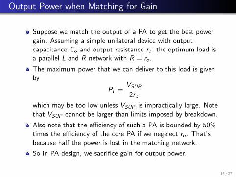
Suppose we match the output of a PA to get the best powergain. Assuming a simple unilateral device with outputcapacitance Co and output resistance ro , the optimum load isa parallel L and R network with R = ro .
The maximum power that we can deliver to this load is givenby
PL =VSUP
2ro
which may be too low unless VSUP is impractically large. Notethat VSUP cannot be larger than limits imposed by breakdown.
Also note that the efficiency of such a PA is bounded by 50%times the efficiency of the core PA if we negelect ro . That’sbecause half the power is lost in the matching network.
So in PA design, we sacrifice gain for output power.
15 / 27
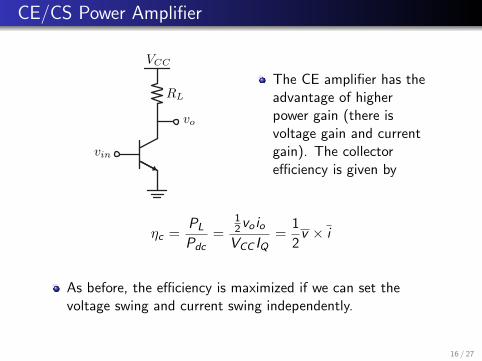
CE/CS Power Amplifier
vin
vo
VCC
RL
The CE amplifier has theadvantage of higherpower gain (there isvoltage gain and currentgain). The collectorefficiency is given by
ηc =PL
Pdc=
12vo io
VCC IQ=
1
2v × i
As before, the efficiency is maximized if we can set thevoltage swing and current swing independently.
16 / 27
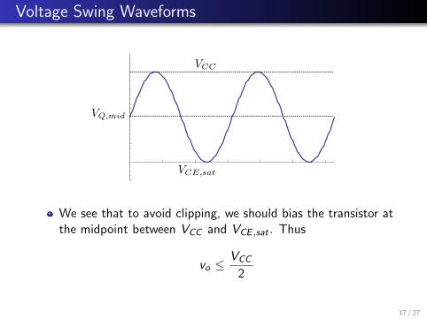
Voltage Swing Waveforms
VCC
VCE,sat
VQ,mid
We see that to avoid clipping, we should bias the transistor atthe midpoint between VCC and VCE ,sat . Thus
vo ≤VCC
2
17 / 27
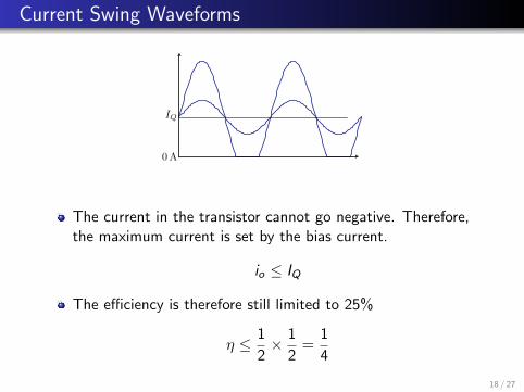
Current Swing Waveforms
IQ
0A
The current in the transistor cannot go negative. Therefore,the maximum current is set by the bias current.
io ≤ IQ
The efficiency is therefore still limited to 25%
η ≤ 1
2× 1
2=
1
4
18 / 27
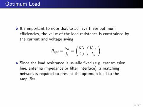
Optimum Load
It’s important to note that to achieve these optimumefficiencies, the value of the load resistance is constrained bythe current and voltage swing
Ropt =voio
=
(v
i
)(VCC
IQ
)Since the load resistance is usually fixed (e.g. transmissionline, antenna impedance or filter interface), a matchingnetwork is required to present the optimum load to theamplifier.
19 / 27
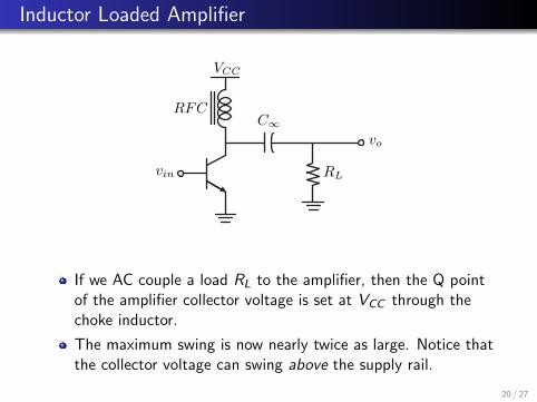
Inductor Loaded Amplifier
vin
vo
VCC
RL
C!RFC
If we AC couple a load RL to the amplifier, then the Q pointof the amplifier collector voltage is set at VCC through thechoke inductor.
The maximum swing is now nearly twice as large. Notice thatthe collector voltage can swing above the supply rail.
20 / 27
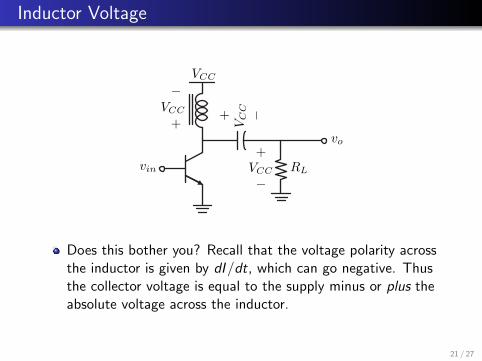
Inductor Voltage
vin
vo
VCC
RL
+VCC
!
+V
CC !VCC
!
+
Does this bother you? Recall that the voltage polarity acrossthe inductor is given by dI/dt, which can go negative. Thusthe collector voltage is equal to the supply minus or plus theabsolute voltage across the inductor.
21 / 27
Collector Inductor Efficiency
Since the swing is almost double, the efficiency nowapproaches 50%
vo ≤ VCC
η =1
2
iovoIQVCC
≤ 1
2
In practice, due to losses in the components and back-off frommaximum swing to minimize distortion, the actual efficiencycan be much lower.
Package parasitics (see later slides) also limit the voltageswing.
22 / 27
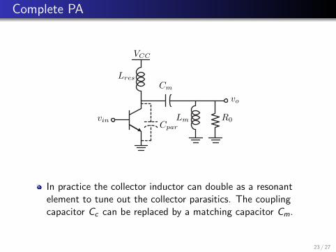
Complete PA
vin
vo
VCC
Lres
Cm
Lm R0Cpar
In practice the collector inductor can double as a resonantelement to tune out the collector parasitics. The couplingcapacitor Cc can be replaced by a matching capacitor Cm.
23 / 27
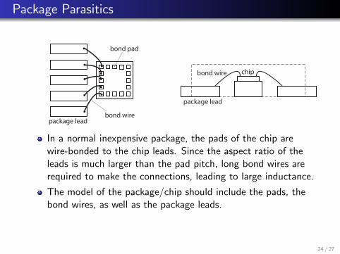
Package Parasitics
bond pad
package leadbond wire
package lead
bond wire chip
In a normal inexpensive package, the pads of the chip arewire-bonded to the chip leads. Since the aspect ratio of theleads is much larger than the pad pitch, long bond wires arerequired to make the connections, leading to large inductance.
The model of the package/chip should include the pads, thebond wires, as well as the package leads.
24 / 27
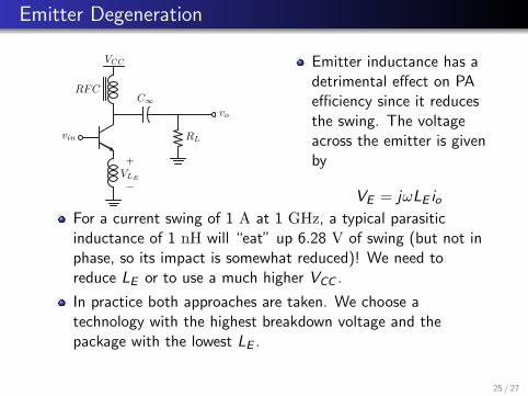
Emitter Degeneration
vin
vo
VCC
RL
C!RFC
+VLE
!
Emitter inductance has adetrimental effect on PAefficiency since it reducesthe swing. The voltageacross the emitter is givenby
VE = jωLE ioFor a current swing of 1 A at 1 GHz, a typical parasiticinductance of 1 nH will “eat” up 6.28 V of swing (but not inphase, so its impact is somewhat reduced)! We need toreduce LE or to use a much higher VCC .
In practice both approaches are taken. We choose atechnology with the highest breakdown voltage and thepackage with the lowest LE .
25 / 27
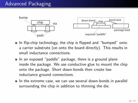
Advanced Packaging
bumpchip via
pads
package lead
bond wirechipdown bond
exposed "paddle"
In flip-chip technology, the chip is flipped and “bumped” ontoa carrier substrate (on onto the board directly). This results insmall inductance connections.
In an exposed “paddle” package, there is a ground planeinside the package. We use conductive glue to mount the chiponto the package. Short down-bonds then create lowinductance ground connections.
In the extreme case, we can use several down-bonds in parallelsurrounding the chip in addition to thinning the die.
26 / 27
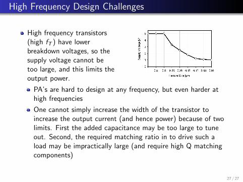
High Frequency Design Challenges
High frequency transistors(high fT ) have lowerbreakdown voltages, so thesupply voltage cannot betoo large, and this limits theoutput power.
PA’s are hard to design at any frequency, but even harder athigh frequencies
One cannot simply increase the width of the transistor toincrease the output current (and hence power) because of twolimits. First the added capacitance may be too large to tuneout. Second, the required matching ratio in to drive such aload may be impractically large (and require high Q matchingcomponents)
27 / 27