P-channel 40 V, 0.0155 typ.,42 A, STripFET F6 Power … · March 2015 DocID025618 Rev 2 1/14 ......
14
March 2015 DocID025618 Rev 2 1/14 This is information on a product in full production. www.st.com STL42P4LLF6 P-channel 40 V, 0.0155 Ω typ.,42 A, STripFET™ F6 Power MOSFET in a PowerFLAT™ 5x6 package Datasheet - production data Figure 1: Internal schematic diagram Features Order code VDS RDS(on) max. ID PTOT STL42P4LLF6 40 V 0.018 Ω 42 A 75 W • Very low on-resistance • Very low gate charge • High avalanche ruggedness • Low gate drive power loss Applications • Switching applications Description This device is a P-channel Power MOSFET developed using the STripFET™ F6 technology, with a new trench gate structure. The resulting Power MOSFET exhibits very low R DS(on) in all packages. For the P-channel Power MOSFET, current polarity of voltages and current have to be reversed. Table 1: Device summary Order code Marking Package Packaging STL42P4LLF6 42P4LLF6 PowerFLAT™ 5x6 Tape and reel 1 2 3 4 PowerFLAT™ 5x6 AM01475v4 D(5, 6, 7, 8) G(4) S(1, 2, 3)
Transcript of P-channel 40 V, 0.0155 typ.,42 A, STripFET F6 Power … · March 2015 DocID025618 Rev 2 1/14 ......

March 2015 DocID025618 Rev 2 1/14
This is information on a product in full production. www.st.com
STL42P4LLF6
P-channel 40 V, 0.0155 Ω typ.,42 A, STripFET™ F6 Power MOSFET in a PowerFLAT™ 5x6 package
Datasheet - production data
Figure 1: Internal schematic diagram
Features Order code VDS RDS(on) max. ID PTOT
STL42P4LLF6 40 V 0.018 Ω 42 A 75 W
• Very low on-resistance • Very low gate charge • High avalanche ruggedness • Low gate drive power loss
Applications • Switching applications
Description This device is a P-channel Power MOSFET developed using the STripFET™ F6 technology, with a new trench gate structure. The resulting Power MOSFET exhibits very low RDS(on) in all packages.
For the P-channel Power MOSFET, current polarity of voltages and current have to be reversed.
Table 1: Device summary Order code Marking Package Packaging
STL42P4LLF6 42P4LLF6 PowerFLAT™ 5x6 Tape and reel
12
34
PowerFLAT™ 5x6
AM01475v4
D(5, 6, 7, 8)
G(4)
S(1, 2, 3)

Contents STL42P4LLF6
2/14 DocID025618 Rev 2
Contents 1 Electrical ratings ............................................................................. 3
2 Electrical characteristics ................................................................ 4
2.1 Electrical characteristics (curves) ...................................................... 6
3 Test circuits ..................................................................................... 8
4 Package mechanical data ............................................................... 9
4.1 PowerFLAT™ 5x6 type R package information ................................ 9
4.2 PowerFLAT™ 5x6 packing information ........................................... 11
5 Revision history ............................................................................ 13
STL42P4LLF6 Electrical ratings
DocID025618 Rev 2 3/14
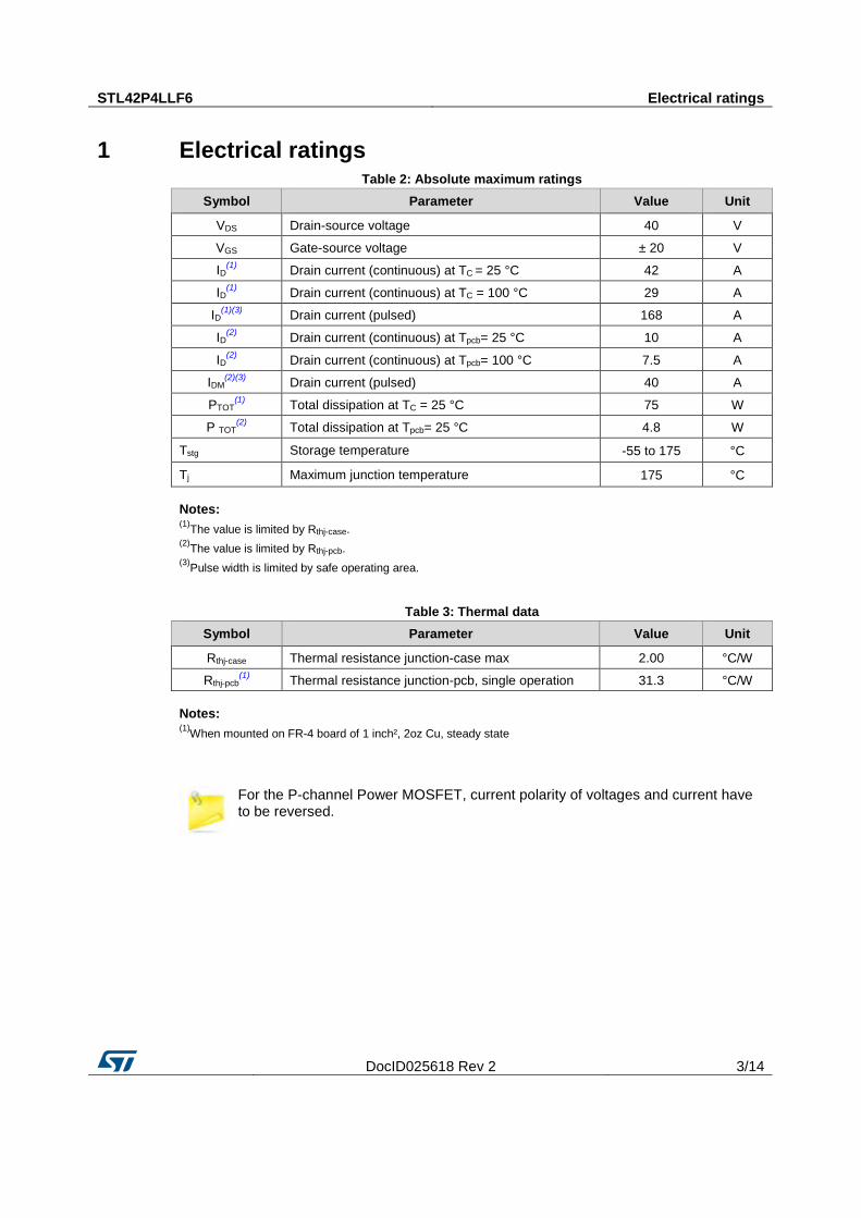
1 Electrical ratings Table 2: Absolute maximum ratings
Symbol Parameter Value Unit
VDS Drain-source voltage 40 V
VGS Gate-source voltage ± 20 V
ID(1) Drain current (continuous) at TC = 25 °C 42 A
ID(1) Drain current (continuous) at TC = 100 °C 29 A
ID(1)(3) Drain current (pulsed) 168 A
ID(2) Drain current (continuous) at Tpcb= 25 °C 10 A
ID(2) Drain current (continuous) at Tpcb= 100 °C 7.5 A
IDM(2)(3) Drain current (pulsed) 40 A
PTOT(1) Total dissipation at TC = 25 °C 75 W
P TOT(2) Total dissipation at Tpcb= 25 °C 4.8 W
Tstg Storage temperature -55 to 175 °C
Tj Maximum junction temperature 175 °C
Notes: (1)The value is limited by Rthj-case. (2)The value is limited by Rthj-pcb. (3)Pulse width is limited by safe operating area.
Table 3: Thermal data Symbol Parameter Value Unit
Rthj-case Thermal resistance junction-case max 2.00 °C/W
Rthj-pcb(1) Thermal resistance junction-pcb, single operation 31.3 °C/W
Notes: (1)When mounted on FR-4 board of 1 inch², 2oz Cu, steady state
For the P-channel Power MOSFET, current polarity of voltages and current have to be reversed.

Electrical characteristics STL42P4LLF6
4/14 DocID025618 Rev 2
2 Electrical characteristics (TC = 25 °C unless otherwise specified)
Table 4: Static
Symbol Parameter Test conditions Min. Typ. Max. Unit
V(BR)DSS Drain-source breakdown voltage VGS = 0 V, ID = 250 µA 40
V
IDSS Zero gate voltage Drain current
VGS = 0 V, VDS = 40 V
1 µA
VGS = 0 V, VDS = 40 V, TC = 125 °C
10 µA
IGSS Gate-body leakage current VDS = 0 V, VGS = ± 20 V
±100 nA
VGS(th) Gate threshold voltage VDS = VGS, ID = 250 µA 1
2.5 V
RDS(on) Static drain-source on-resistance
VGS = 10 V, ID = 5 A
0.0105 0.018 Ω
VGS = 4.5 V, ID= 5 A
0.021 0.026
Table 5: Dynamic Symbol Parameter Test conditions Min. Typ. Max. Unit
Ciss Input capacitance
VDS = 25 V, f = 1 MHz, VGS = 0 V
- 2850 - pF
Coss Output capacitance - 270 - pF
Crss Reverse transfer capacitance - 180 - pF
Qg Total gate charge VDD = 20 V, ID = 10 A, VGS = 4.5 V (see Figure 14: "Gate charge test circuit")
- 22 - nC
Qgs Gate-source charge - 9.4 - nC
Qgd Gate-drain charge - 7.3 - nC
RG Gate input resistance
ID = 0 A, gate DC bias = 0 V, f = 1 MHz, magnitude of alternative signal = 20 mV
- 1.4 - Ω
Table 6: Switching times
Symbol Parameter Test conditions Min. Typ. Max. Unit
td(on) Turn-on delay time VDD = 20 V, ID = 5 A RG = 4.7 Ω, VGS = 10 V (see Figure 13: "Switching times test circuit for resistive load")
- 43 - ns
tr Rise time - 47 - ns
td(off) Turn-off-delay time - 148 - ns
tf Fall time - 19 - ns
For the P-channel Power MOSFET, current polarity of voltages and current have to be reversed.
STL42P4LLF6 Electrical characteristics
DocID025618 Rev 2 5/14
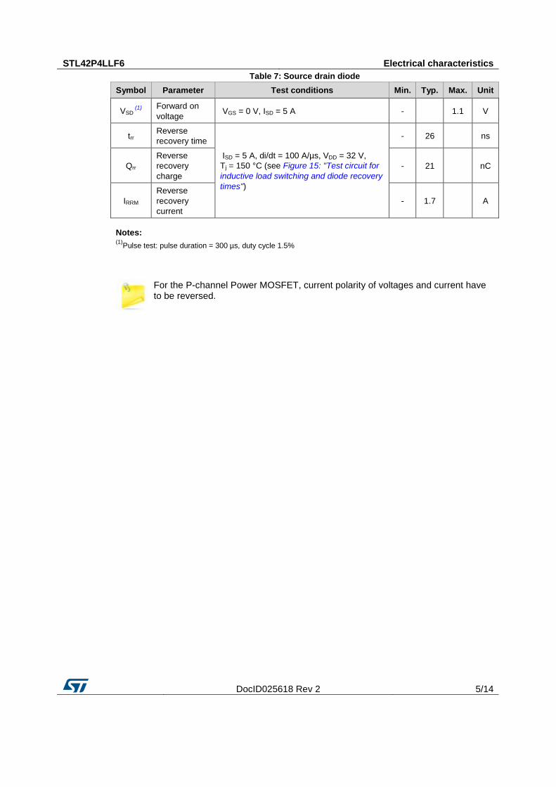
Table 7: Source drain diode Symbol Parameter Test conditions Min. Typ. Max. Unit
VSD (1) Forward on
voltage VGS = 0 V, ISD = 5 A -
1.1 V
trr Reverse recovery time
ISD = 5 A, di/dt = 100 A/µs, VDD = 32 V, Tj = 150 °C (see Figure 15: "Test circuit for inductive load switching and diode recovery times")
- 26
ns
Qrr Reverse recovery charge
- 21
nC
IRRM Reverse recovery current
- 1.7
A
Notes: (1)Pulse test: pulse duration = 300 µs, duty cycle 1.5%
For the P-channel Power MOSFET, current polarity of voltages and current have to be reversed.

Electrical characteristics STL42P4LLF6
6/14 DocID025618 Rev 2
2.1 Electrical characteristics (curves) Figure 2: Safe operating area
Figure 3: Thermal impedance
Figure 4: Output characteristics
Figure 5: Transfer characteristics
Figure 6: Normalized gate threshold voltage vs temperature
Figure 7: Normalized V(BR)DSS vs temperature

STL42P4LLF6 Electrical characteristics
DocID025618 Rev 2 7/14
Figure 8: Static drain-source on-resistance
Figure 9: Normalized on-resistance vs. temperature
Figure 10: Gate charge vs gate-source voltage
Figure 11: Capacitance variations voltage
Figure 12: Source-drain diode forward characteristics
Test circuits STL42P4LLF6
8/14 DocID025618 Rev 2
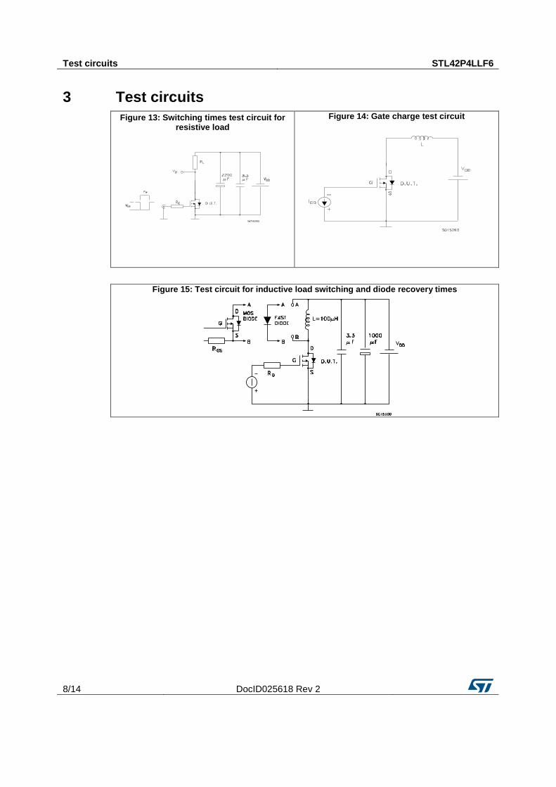
3 Test circuits Figure 13: Switching times test circuit for
resistive load
Figure 14: Gate charge test circuit
Figure 15: Test circuit for inductive load switching and diode recovery times
STL42P4LLF6 Package mechanical data
DocID025618 Rev 2 9/14
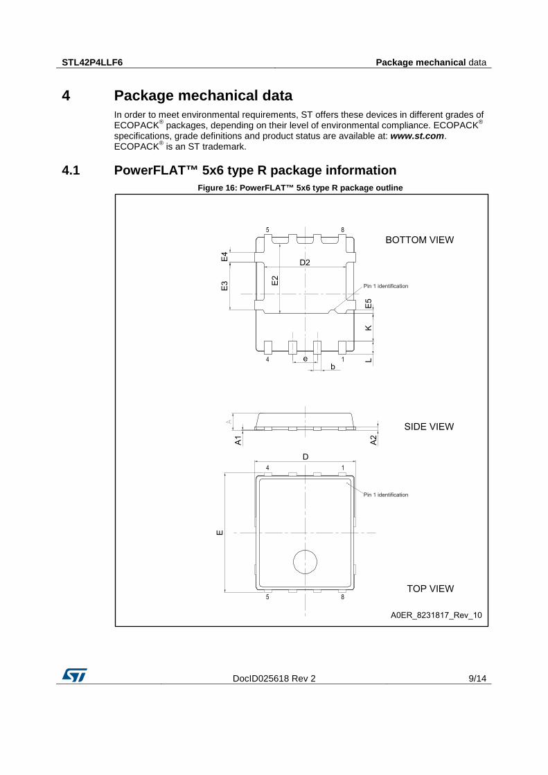
4 Package mechanical data In order to meet environmental requirements, ST offers these devices in different grades of ECOPACK® packages, depending on their level of environmental compliance. ECOPACK® specifications, grade definitions and product status are available at: www.st.com. ECOPACK® is an ST trademark.
4.1 PowerFLAT™ 5x6 type R package information Figure 16: PowerFLAT™ 5x6 type R package outline

Package mechanical data STL42P4LLF6
10/14 DocID025618 Rev 2
Table 8: PowerFLAT™ 5x6 type R mechanical data
Dim. mm
Min. Typ. Max.
A 0.80
1.00
A1 0.02
0.05
A2
0.25
b 0.30
0.50
D 5.00 5.20 5.40
E 5.95 6.15 6.35
D2 4.11
4.31
e
1.27
L 0.60
0.80
K 1.275
1.575
E3 2.35
2.55
E4 0.40
0.60
E5 0.08
0.28
Figure 17: PowerFLAT™ 5x6 recommended footprint (dimensions are in mm)

STL42P4LLF6 Package mechanical data
DocID025618 Rev 2 11/14
4.2 PowerFLAT™ 5x6 packing information Figure 18: PowerFLAT™ 5x6 tape (dimensions are in mm)
Figure 19: PowerFLAT™ 5x6 package orientation in carrier tape
Measured from centerline of sprocket holeto centerline of pocket.Cumulative tolerance of 10 sprocketholes is ± 0.20 .Measured from centerline of sprockethole to centerline of pocket.
(I)
(II)
(III)
2
2.0±0.1 (I)
Bo
(5.3
0±0.
1)
Ko (1.20±0.1)
±0.05)
Ø1.5 MIN.
Ø1.55±0.05
P
Ao(6.30±0.1)
F(5.
50±0
.1)(I
II)
W(1
2.00
±0.3
)
1.75±0.1
4.0±0.1 (II)P 0
Y
Y
SECTION Y-Y
CL
P1(8.00±0.1)
Do
D1
E1(0.30
T
REF.R0.50
REF 0.20
Base and bulk quantity 3000 pcs
8234350_Tape_rev_C

Package mechanical data STL42P4LLF6
12/14 DocID025618 Rev 2
Figure 20: PowerFLAT™ 5x6 reel
STL42P4LLF6 Revision history
DocID025618 Rev 2 13/14
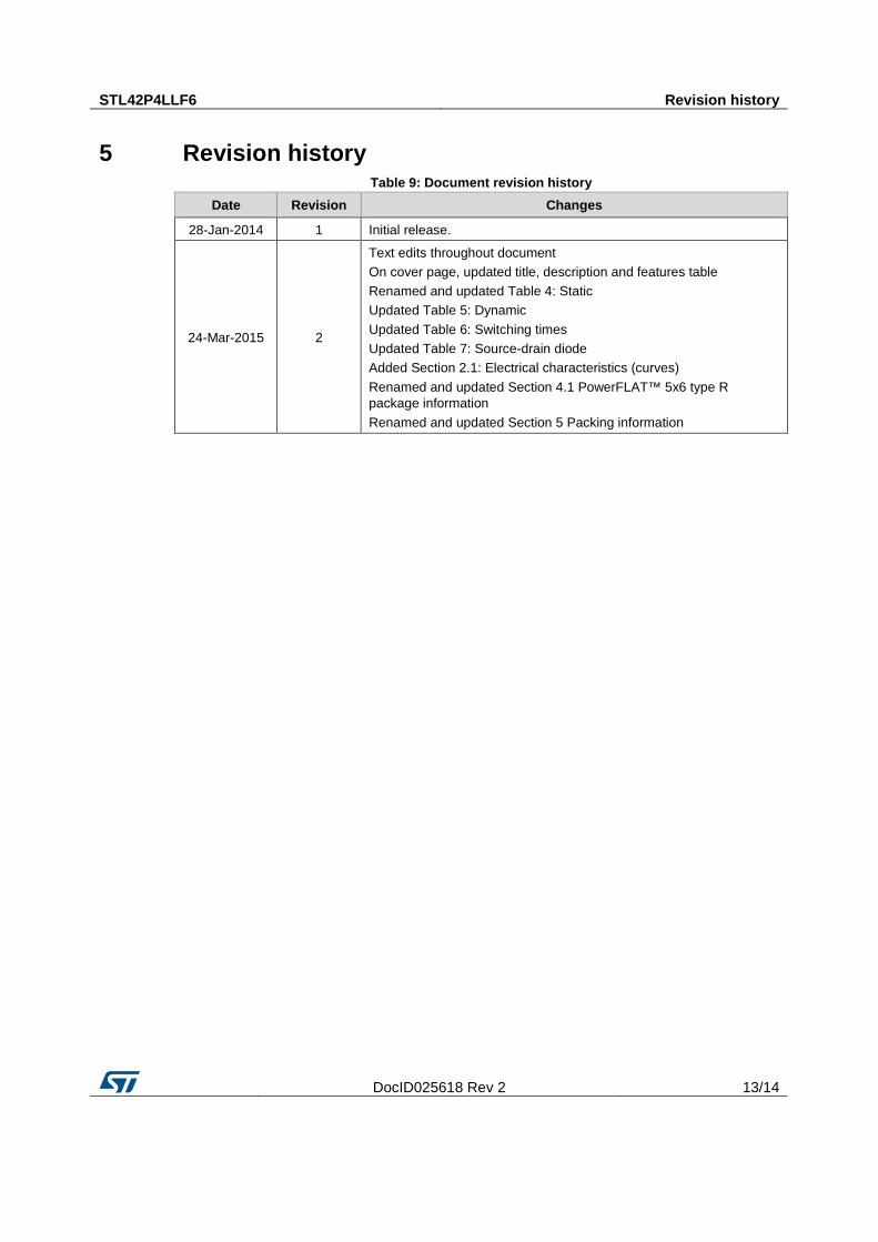
5 Revision history Table 9: Document revision history
Date Revision Changes
28-Jan-2014 1 Initial release.
24-Mar-2015 2
Text edits throughout document On cover page, updated title, description and features table Renamed and updated Table 4: Static Updated Table 5: Dynamic Updated Table 6: Switching times Updated Table 7: Source-drain diode Added Section 2.1: Electrical characteristics (curves) Renamed and updated Section 4.1 PowerFLAT™ 5x6 type R package information Renamed and updated Section 5 Packing information
STL42P4LLF6
14/14 DocID025618 Rev 2
IMPORTANT NOTICE – PLEASE READ CAREFULLY
STMicroelectronics NV and its subsidiaries (“ST”) reserve the right to make changes, corrections, enhancements, modifications, and improvements to ST products and/or to this document at any time without notice. Purchasers should obtain the latest relevant information on ST products before placing orders. ST products are sold pursuant to ST’s terms and conditions of sale in place at the time of order acknowledgement.
Purchasers are solely responsible for the choice, selection, and use of ST products and ST assumes no liability for application assistance or the design of Purchasers’ products.
No license, express or implied, to any intellectual property right is granted by ST herein.
Resale of ST products with provisions different from the information set forth herein shall void any warranty granted by ST for such product.
ST and the ST logo are trademarks of ST. All other product or service names are the property of their respective owners.
Information in this document supersedes and replaces information previously supplied in any prior versions of this document.
© 2015 STMicroelectronics – All rights reserved