Organic Semiconductors: Electronic Properties and Optoelectronic Applications Hsiang-Han Tseng.
12
Organic Semiconductors: Electronic Properties and Optoelectronic Applications Hsiang-Han Tseng
-
date post
22-Dec-2015 -
Category
Documents
-
view
230 -
download
2
Transcript of Organic Semiconductors: Electronic Properties and Optoelectronic Applications Hsiang-Han Tseng.
Organic Semiconductors: Electronic Properties and
Optoelectronic Applications
Hsiang-Han Tseng
Overview
• Organic Semiconductors • Electronic Properties • Fundamentals of Organic PV Cells • Examples
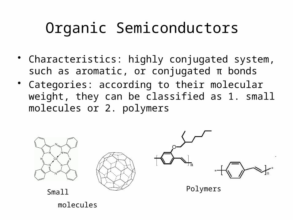
Organic Semiconductors
• Characteristics: highly conjugated system, such as aromatic, or conjugated π bonds
• Categories: according to their molecular weight, they can be classified as 1. small molecules or 2. polymers
Small molecules Polymers
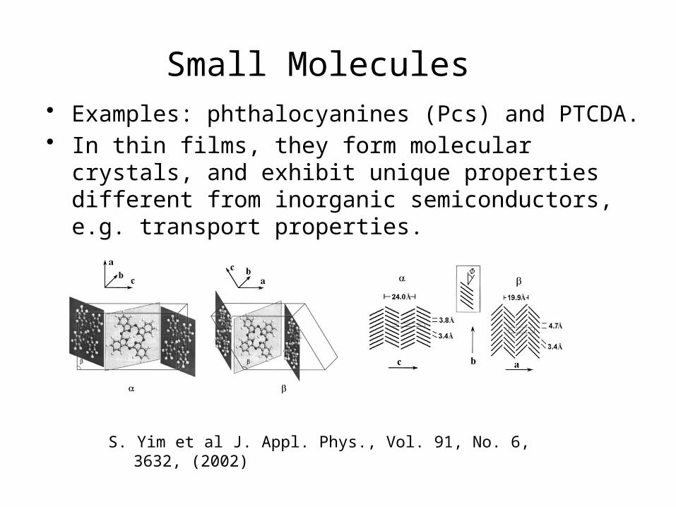
Small Molecules • Examples: phthalocyanines (Pcs) and PTCDA.• In thin films, they form molecular crystals, and exhibit
unique properties different from inorganic semiconductors, e.g. transport properties.
S. Yim et al J. Appl. Phys., Vol. 91, No. 6, 3632, (2002)
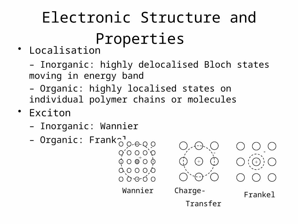
Electronic Structure and Properties • Localisation
– Inorganic: highly delocalised Bloch states moving in energy band
– Organic: highly localised states on individual polymer chains or molecules
• Exciton – Inorganic: Wannier
– Organic: Frankel
Charge-Transfer Wannier Frankel
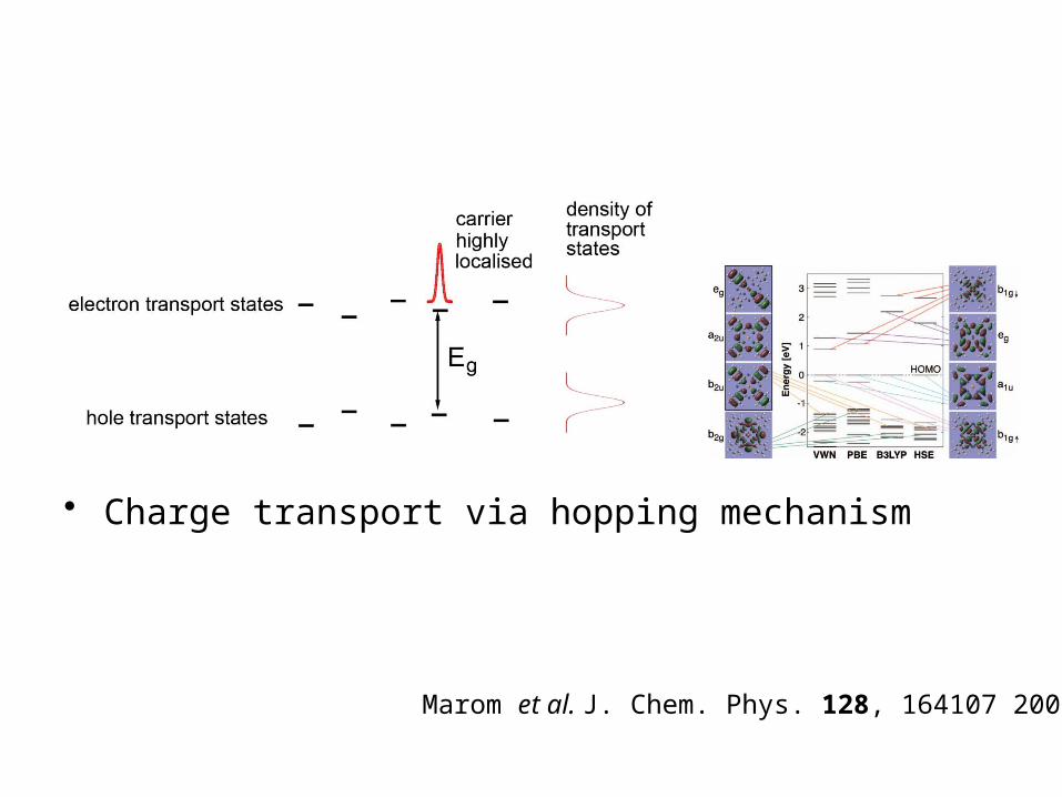
• Charge transport via hopping mechanism
Marom et al. J. Chem. Phys. 128, 164107 2008
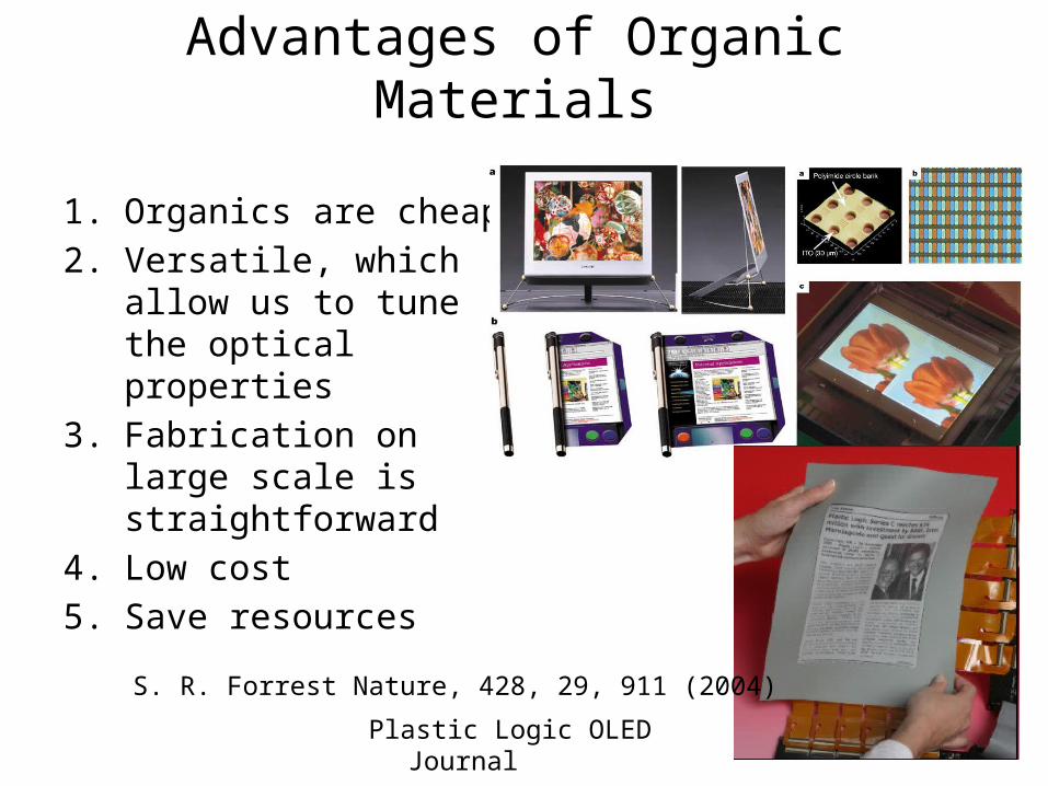
Advantages of Organic Materials
1. Organics are cheap
2. Versatile, which allow us to tune the optical properties
3. Fabrication on large scale is straightforward
4. Low cost
5. Save resources
S. R. Forrest Nature, 428, 29, 911 (2004)
Plastic Logic OLED Journal
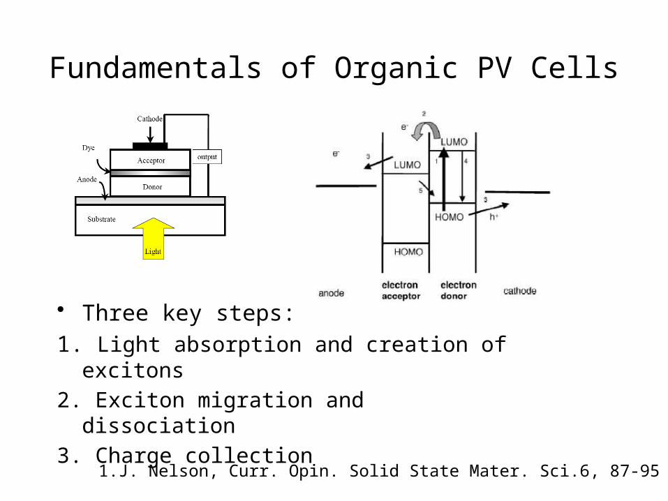
Fundamentals of Organic PV Cells
• Three key steps:
1. Light absorption and creation of excitons
2. Exciton migration and dissociation
3. Charge collection
1.J. Nelson, Curr. Opin. Solid State Mater. Sci.6, 87-95 (2002)
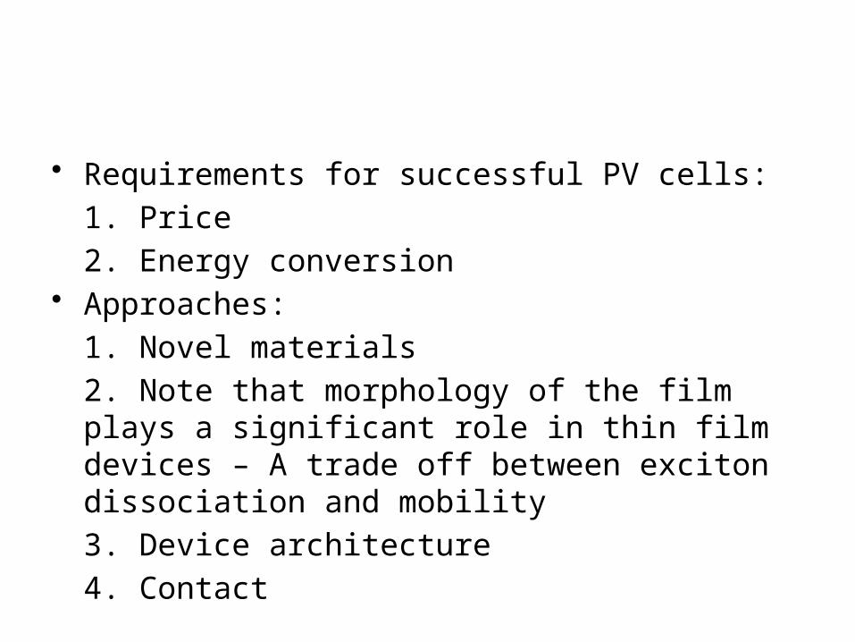
• Requirements for successful PV cells:
1. Price
2. Energy conversion • Approaches:
1. Novel materials
2. Note that morphology of the film plays a significant role in thin film devices – A trade off between exciton dissociation and mobility
3. Device architecture
4. Contact
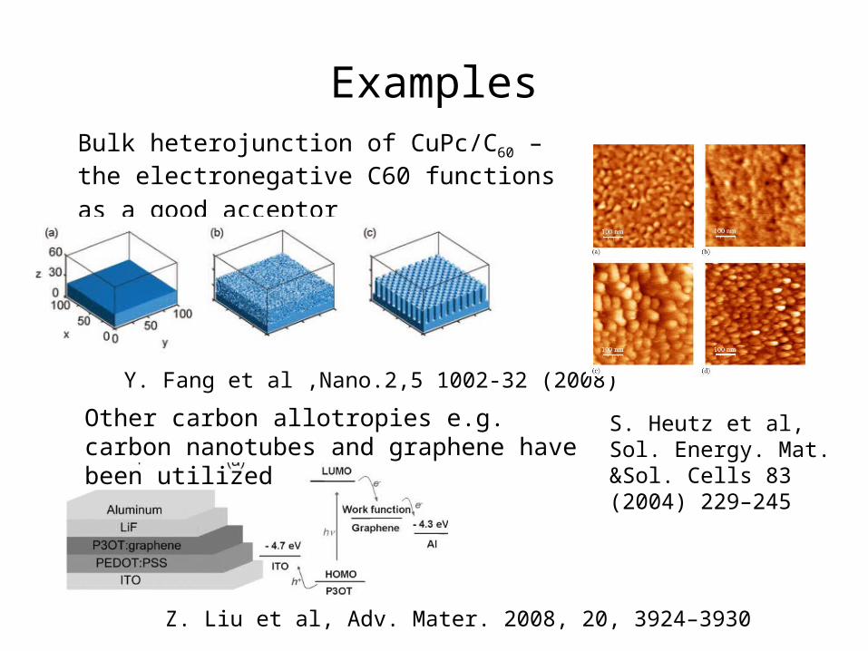
Examples Bulk heterojunction of CuPc/C60 – the
electronegative C60 functions as a good
acceptor
Y. Fang et al ,Nano.2,5 1002-32 (2008)
S. Heutz et al, Sol. Energy. Mat. &Sol. Cells 83 (2004) 229–245
Z. Liu et al, Adv. Mater. 2008, 20, 3924–3930
Other carbon allotropies e.g. carbon nanotubes and graphene have been utilized
Conclusion
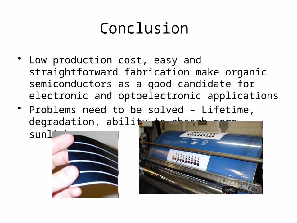
• Low production cost, easy and straightforward fabrication make organic semiconductors as a good candidate for electronic and optoelectronic applications
• Problems need to be solved – Lifetime, degradation, ability to absorb more sunlight

• Thank you for your attention.