Optical Properties of Lattice Vibrationscmyles/Phys5335/Lectures/Optical Properties 3...Lectures on...
29
Lectures on Semiconductor Physics & Materials 2009 Lecture 16 1 Optical Properties of Lattice Vibrations For a collection of classical charged Simple Harmonic Oscillators, the dielectric function is given by: Where N i is the number of oscillators with frequency ω i and e is the charge of the oscillators
Transcript of Optical Properties of Lattice Vibrationscmyles/Phys5335/Lectures/Optical Properties 3...Lectures on...
Lectures on Semiconductor Physics & Materials
2009 Lecture 16 1
Optical Properties of Lattice Vibrations
For a collection of classical charged Simple Harmonic Oscillators, the dielectric function is given by:
Where Ni is the number of oscillators with frequency ωi and e is the charge of the oscillators
Lectures on Semiconductor Physics & Materials
2009 Lecture 16 2
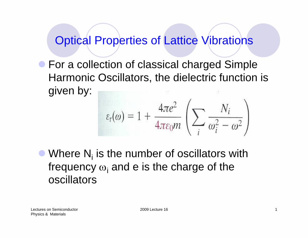
Optical Properties of Lattice VibrationsFor optical phonons it is necessary to consider that the polarization is now in the form of a wave and also the effect of retardation.A wave has a wave vector k which determines whether the wave is transverse ( E┴k) or longitudinal (E||k)In the absence of free charges the medium has to satisfy the Gauss theorem: ∇•D=0 or ε(k•Eo)=0.If the EM wave is a plane wave described by:E=Eoexp[i(k•r-ωt)] then the equation ε(k•Eo)=0 can
be satisfied either by:ε=0 or (k•Eo)=0
Lectures on Semiconductor Physics & Materials
2009 Lecture 16 3
Optical Properties of Lattice Vibrations
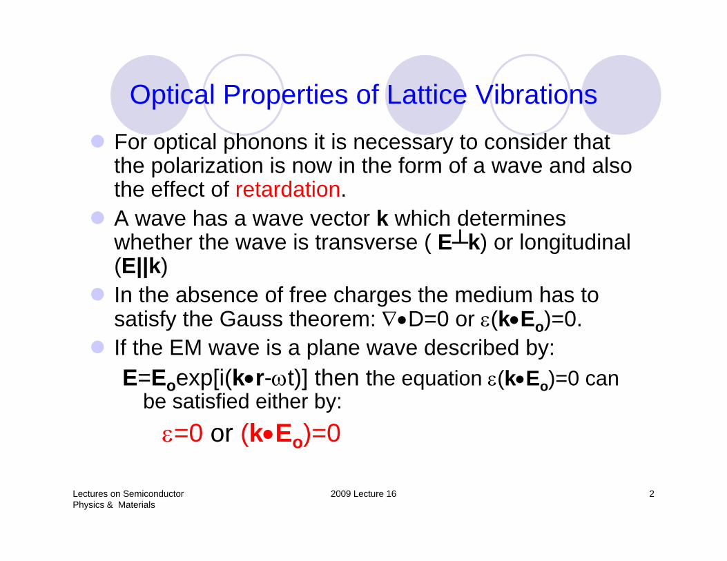
When (k•Eo)=0 the EM wave is transverse and since P~E the polarization wave induced is also transverse.For a longitudinal wave (k•Eo)≠0 so ε=0. The frequency of this longitudinal wave will be denoted by ωL and it is given by the frequency when ε(ωL)=0
Lectures on Semiconductor Physics & Materials
2009 Lecture 16 4
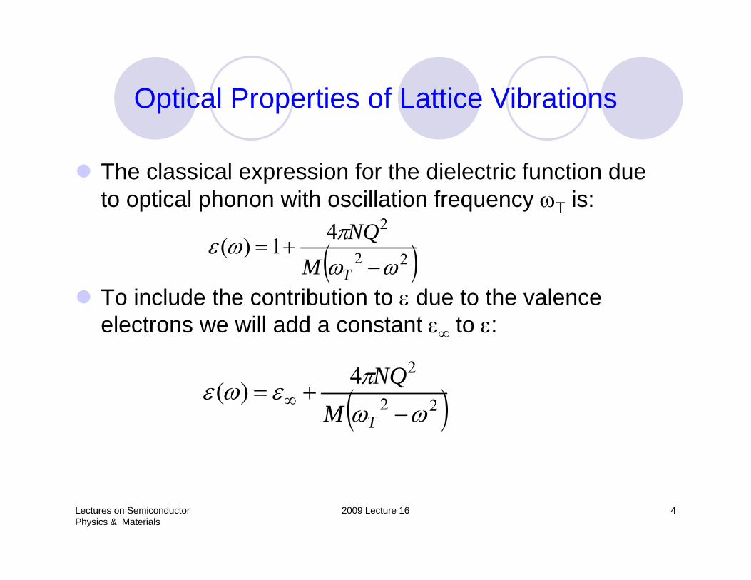
Optical Properties of Lattice Vibrations
The classical expression for the dielectric function due to optical phonon with oscillation frequency ωT is:
To include the contribution to ε due to the valence electrons we will add a constant ε∞ to ε:
( )22
241)(ωω
πωε−
+=TMNQ
( )22
24)(ωω
πεωε−
+= ∞TMNQ
Lectures on Semiconductor Physics & Materials
2009 Lecture 16 5
Optical Properties of Lattice Vibrations
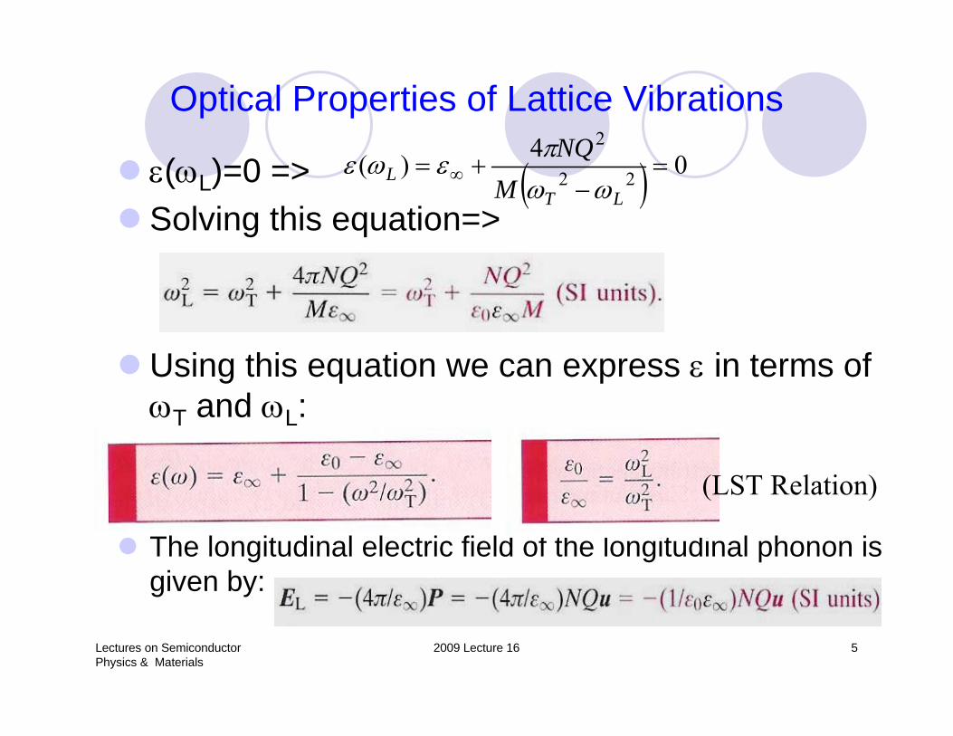
ε(ωL)=0 =>Solving this equation=>
Using this equation we can express ε in terms of ωT and ωL:
The longitudinal electric field of the longitudinal phonon is given by:
( ) 04)( 22
2=
−+= ∞
LTL
MNQ
ωωπεωε
(LST Relation)
Lectures on Semiconductor Physics & Materials
2009 Lecture 16 6
Optical Properties of Lattice Vibrations
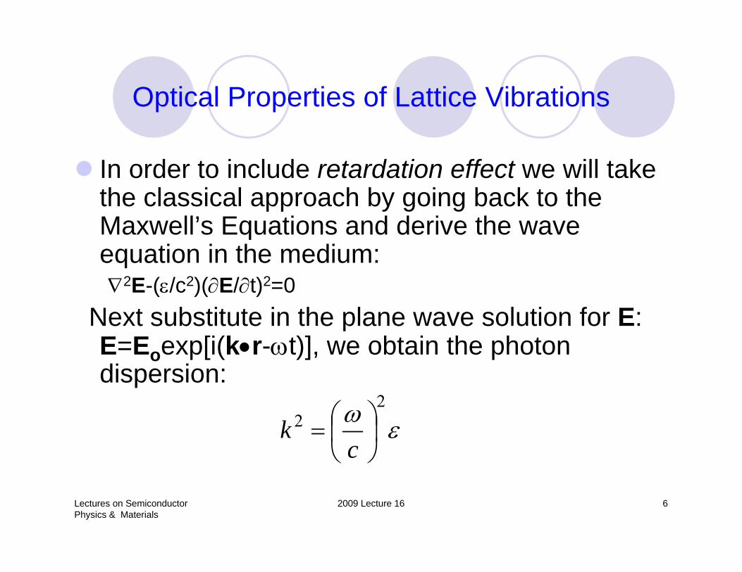
In order to include retardation effect we will take the classical approach by going back to the Maxwell’s Equations and derive the wave equation in the medium:∇2E-(ε/c2)(∂E/∂t)2=0
Next substitute in the plane wave solution for E: E=Eoexp[i(k•r-ωt)], we obtain the photon dispersion:
εω 22 ⎟
⎠⎞
⎜⎝⎛=
ck
Lectures on Semiconductor Physics & Materials
2009 Lecture 16 7
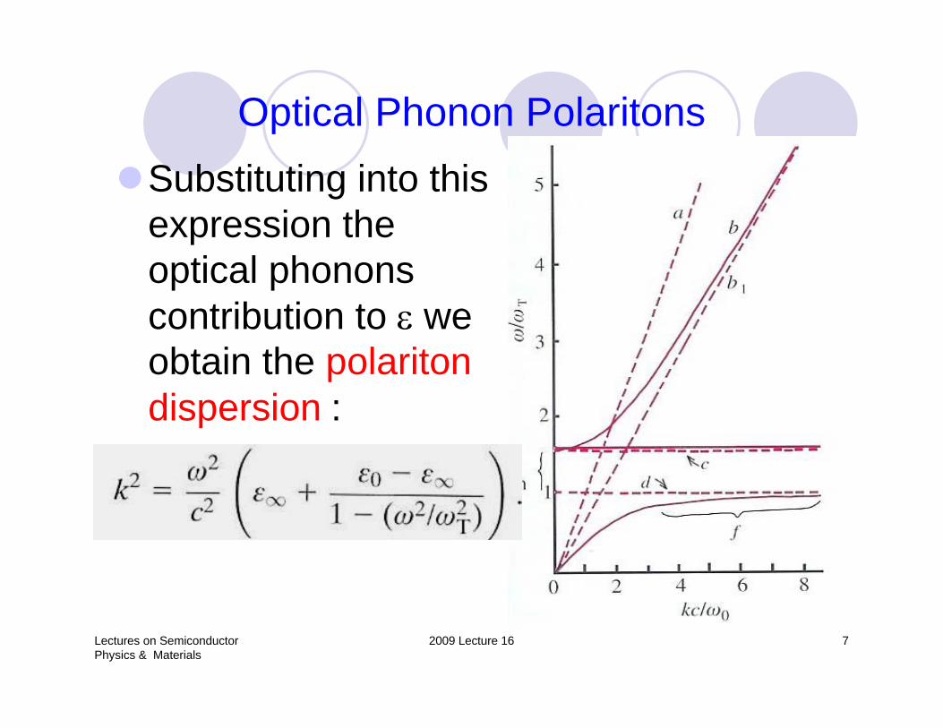
Optical Phonon PolaritonsSubstituting into this expression the optical phonons contribution to ε we obtain the polaritondispersion :
Lectures on Semiconductor Physics & Materials
2009 Lecture 16 8
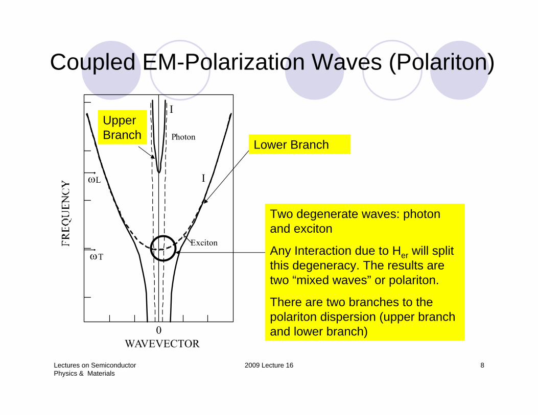
Coupled EM-Polarization Waves (Polariton)
Photon
Exciton
0
I
I
ωT
ωL
WAVEVECTOR
Two degenerate waves: photon and exciton
Any Interaction due to Her will split this degeneracy. The results are two “mixed waves” or polariton.
There are two branches to the polariton dispersion (upper branch and lower branch)
Lower Branch
Upper Branch
Lectures on Semiconductor Physics & Materials
2009 Lecture 16 9
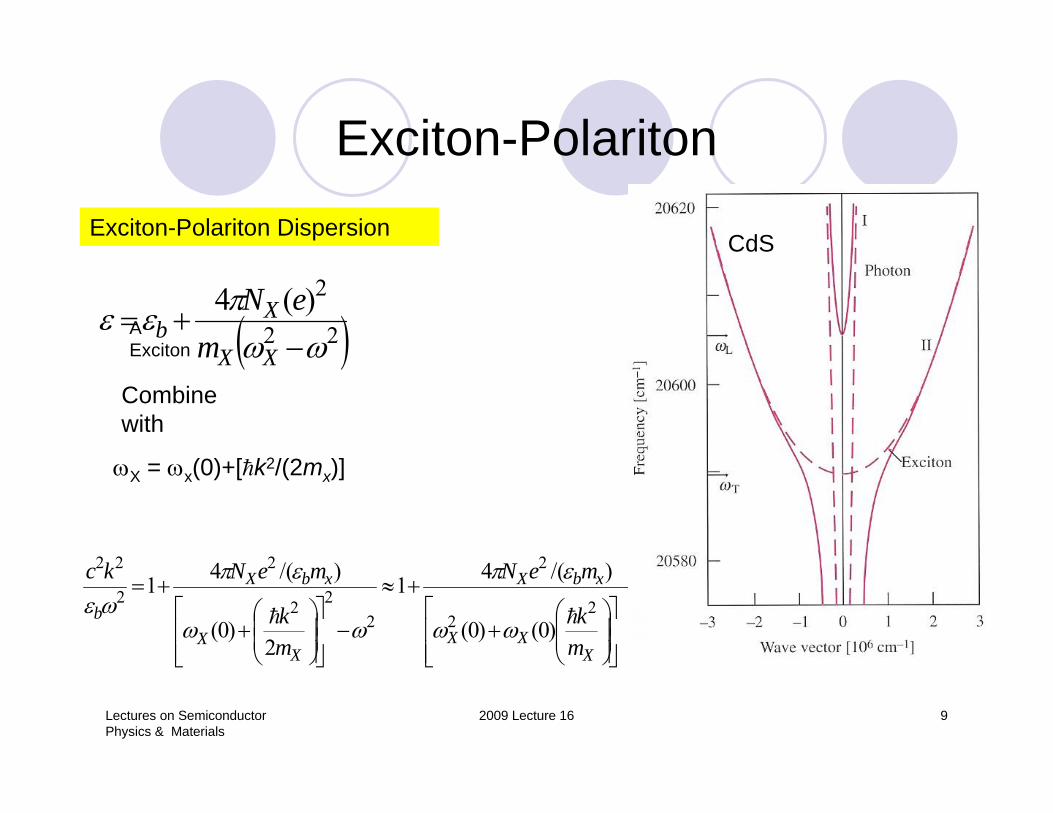
Exciton-Polariton
( )22
2)(4ωω
πεε−
+=XX
Xb m
eN
ωX = ωx(0)+[hk2/(2mx)]
22
2
2
222
2
2
22
)0()0(
)/(41
2)0(
)/(41
ωωω
επ
ωω
επωε
−⎥⎥⎦
⎤
⎢⎢⎣
⎡⎟⎟⎠
⎞⎜⎜⎝
⎛+
+≈
−⎥⎥⎦
⎤
⎢⎢⎣
⎡⎟⎟⎠
⎞⎜⎜⎝
⎛+
+=
XXX
xbX
XX
xbX
b
mk
meN
mk
meNkc
hh
Combine with
Exciton-Polariton Dispersion
A Exciton
CdS
Lectures on Semiconductor Physics & Materials
2009 Lecture 16 10
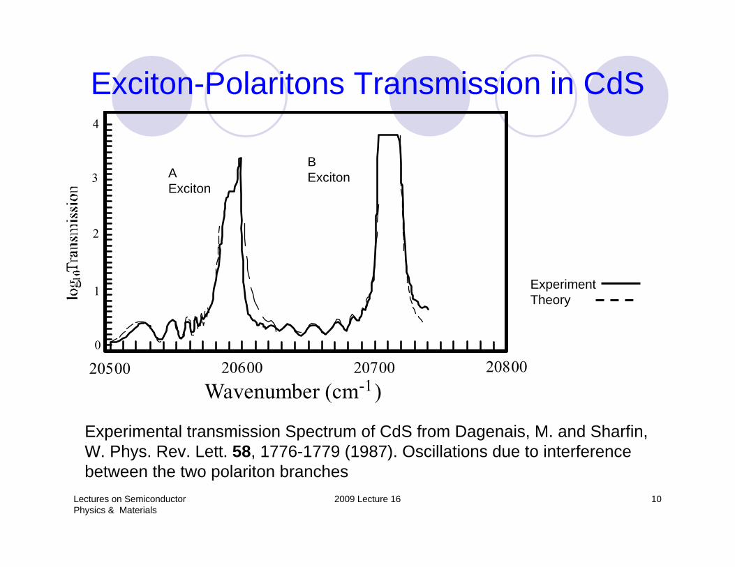
Exciton-Polaritons Transmission in CdS
Wavenumber (cm )-120500 20600 20700 208000
1
2
3
4
ExperimentTheory
A Exciton
B Exciton
Experimental transmission Spectrum of CdS from Dagenais, M. and Sharfin, W. Phys. Rev. Lett. 58, 1776-1779 (1987). Oscillations due to interference between the two polariton branches
Lectures on Semiconductor Physics & Materials
2009 Lecture 16 11
Absorption in the Polariton Picture
Polariton is a propagating wave in a medium. External wave is converted into a polariton inside the medium with a reflection and transmission coefficients.Absorption occurs when polaritons are scattered or disappear inside the medium (note the similarity between this case and the Landauer-Büttikerformalism for transport of charges)Since excitons and phonons are more strongly scattered, dissipation of polaritons is usually dominated by the polarization component of the polariton
Lectures on Semiconductor Physics & Materials
2009 Lecture 16 12
Cavity PolaritonsPolaritons (as a form of coupled mode) can also exist in micro-cavitiesIn cavities the EM modes are confined in one or more directions but in most cases can propagate as a wave in at least one direction. When these cavity modes (either standing or guided waves) resonate with excitons in the medium, coupled EM-polarization modes, known as cavity polaritons, are formed.Cavity polaritons are important for understand the properties of a class of lasers known as vertically integrated cavity surface emitting lasers (VICSEL) which contain micro-cavities formed by Bragg reflectors.
Lectures on Semiconductor Physics & Materials
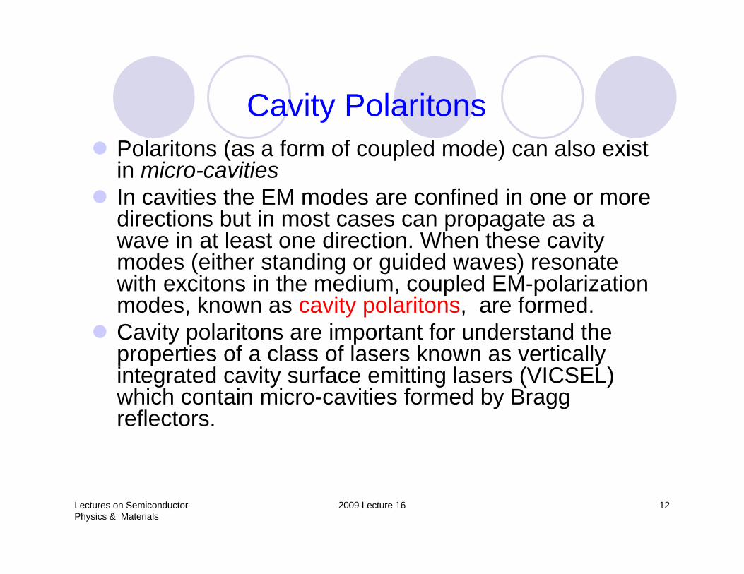
2009 Lecture 16 13
PolaritonReflection
from a Micro-cavity
Reference: Phys. Rev. Lett. 90, 116401 (2003)
Lectures on Semiconductor Physics & Materials
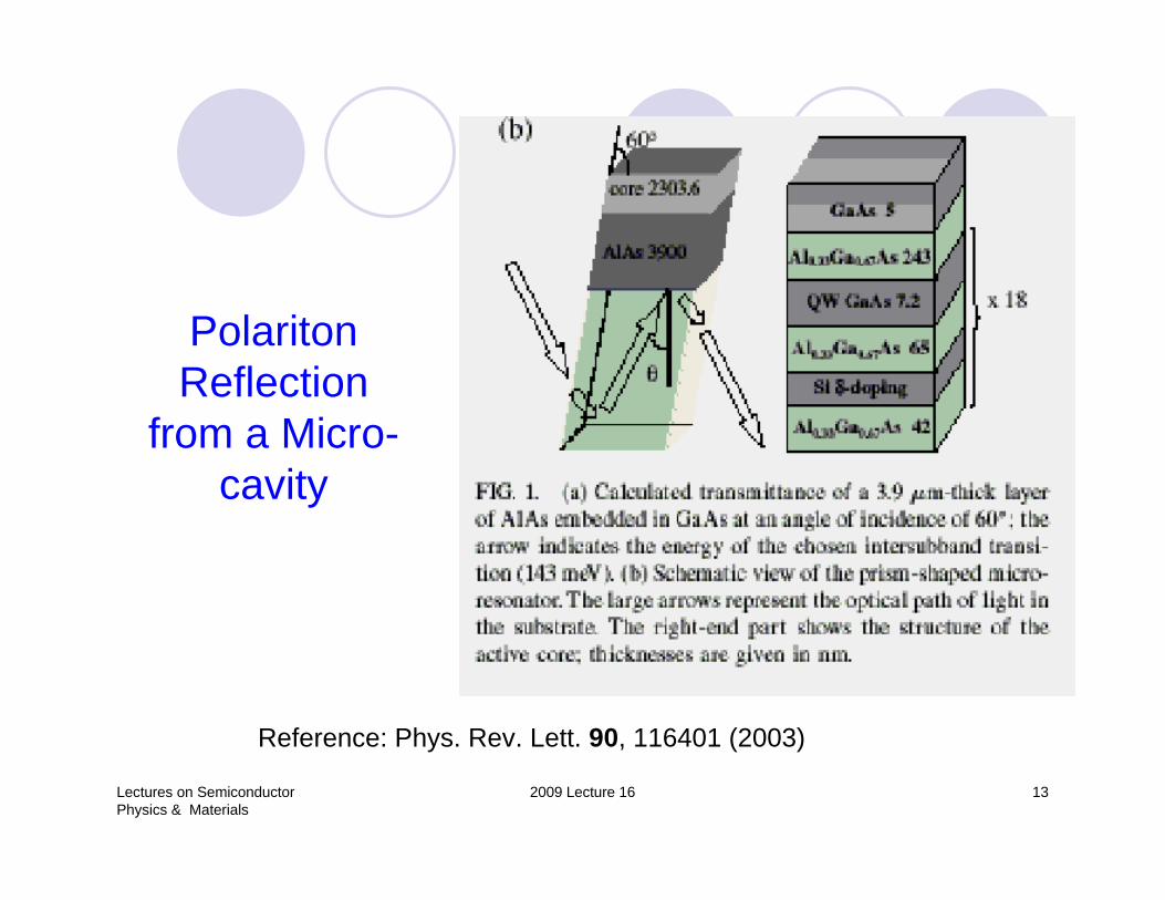
2009 Lecture 16 14
PolaritonReflection from a Micro-cavity
Lectures on Semiconductor Physics & Materials
2009 Lecture 16 15
Theory of EmissionClassically emission of light is a common everyday experienceClassical theory: an oscillating dipole will radiate EM wave so the medium must be excited firstEmission excited by
light photoluminescenceElectrons electroluminescencHeating thermoluminescenceSound wave sonoluminescence
The semiclassical approach we have adopted cannot explain spontaneous emission since there is no EM field before emission making the interaction Hamiltonian between electron and EM field=0
Lectures on Semiconductor Physics & Materials
2009 Lecture 16 16
Theory of EmissionThis problem is solved when we quantize the EM wave into photons.Probability of creating a photon is proportional to (1+N) where N is the photon occupancy: N=1/[exp(hω)/KbT-1]. The constant of proportionality is same as that for annihilation of a photon or absorption. Notice that even if N=0 there is still a non-zero probability of emitting a photon. Thus if the probability of absorbing a photon is given by BN, the probability for spontaneous emission is A while the probability for stimulated emission is AN. A and B are known as the Einstein’s A and B coefficients and are related to each other by the photon energy density. The reason is because the incident EM wave usually has a well-defined k but in emission the EM wave is emitted in all directions.
Lectures on Semiconductor Physics & Materials
2009 Lecture 16 17
Einstein Theory of Stimulated EmissionEinstein did not believe in Quantum Mechanics but he was able to derive the QM result before the development of QM.Einstein used Boltzmann’s theory of statistical mechanics and Planck’s radiation laws to argue that an electron with two levels cannot be in thermal equilibrium with a radiation field without stimulated emissionThe reason is: rate of absorption is proportional to intensity of light. If emission is entirely due to spontaneous emission, its rate is independent of intensity. By increasing the intensity one can make the excited state population larger than the ground state population violation of Boltzmann’s result that the excited state population is smaller than the ground state population by the factor : exp[-ΔE/KbT].
Lectures on Semiconductor Physics & Materials
2009 Lecture 16 18
Einstein’s A & B coefficients
Let |n> and |m> represent 2 non-degenerate levels with En>Em. The rate for absorption (transition from |m> to |n>) for unit of incident EM energy density is Bmn and is equal to the rate for the reverse process (stimulated emission) Bnm. The rate for spontaneous emission is given by Anm and since spontaneous emission is spread over all directions the emission rate per unit EM energy density=Anm/ρ(ν) where ρ(ν) is energy density of the EM wave with frequency between ν and ν+Δν and is given by: Np(hν) (8πν2) (n/c)3.
Lectures on Semiconductor Physics & Materials
2009 Lecture 16 19
Einstein’s A & B coefficients
Using the Principle of Detailed Balance Einstein obtained: Bmn = Bnm and Anm =(8πhν3) (n/c)3 BnmFrom Einstein’s result the total rate of emission is:Anm + Bnm ρ= Anm(1+ρBnm /Anm)
= Anm(1+Np)The rate of absorption is Bnm ρ= Anm ΝpΤhis is exactly the same result as obtained by
QM!
Lectures on Semiconductor Physics & Materials
2009 Lecture 16 20
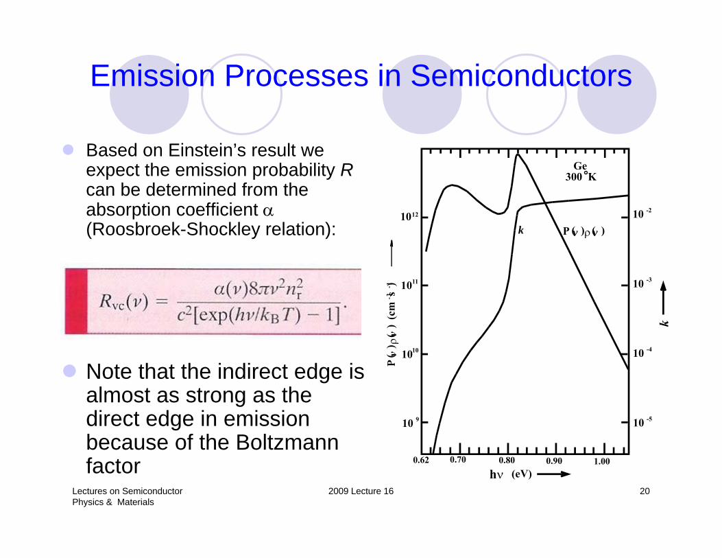
Emission Processes in Semiconductors
Based on Einstein’s result we expect the emission probability Rcan be determined from the absorption coefficient α (Roosbroek-Shockley relation):
Note that the indirect edge is almost as strong as the direct edge in emission because of the Boltzmannfactor
Ge300 K
k10
10
10
10
12
11
10
9
0.62 0.70 0.80 0.90 1.00
( )( )v vP ρ
hν (eV)
10 -5
10 -4
10 -3
10 -2
Lectures on Semiconductor Physics & Materials
2009 Lecture 16 21
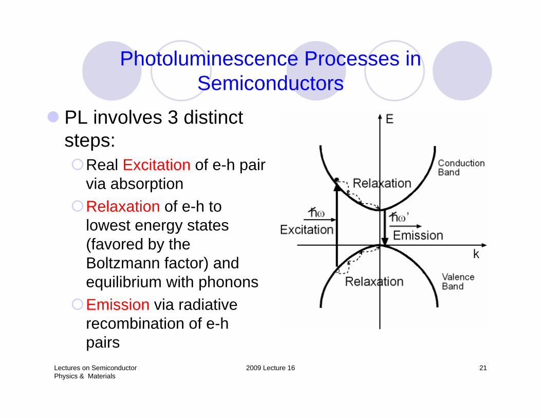
Photoluminescence Processes in Semiconductors
PL involves 3 distinct steps:
Real Excitation of e-h pair via absorptionRelaxation of e-h to lowest energy states (favored by the Boltzmann factor) and equilibrium with phononsEmission via radiativerecombination of e-hpairs
Lectures on Semiconductor Physics & Materials
2009 Lecture 16 22
Emission Processes in Semiconductors
In pure semiconductors emission is intrinsic and dominated by recombination of free excitons at low T and conduction band-to-valence band transition at high TIn extrinsic semiconductors emission is dominated by defects and impurities:
Excitons bound to donors, acceptors or neutral centersFree-to-bound transitions such as donor=>valence bandDonor-acceptor pair (DAP) transitions
Since the Boltzmann factor tends to favor low energy states emission is a very sensitive probe of defect and impurity states
Lectures on Semiconductor Physics & Materials
2009 Lecture 16 23
Free-to-bound transitions in Doped Semiconductors and Mott transition
Electrons in Shallow Donors have Bohr radii typically of the order of tens of lattice constants (or ~ several nm to 10 nm). When their concentration is high enough these electron wave function will overlap and electrons from one donor can hop to another. In another word the semiconductor becomes metallic and the discrete impurity levels will form bands, known as impurity bands. This transition from an insulating to a metallic state is known as Mott Transition. It is a classic example of a many-body effect and quantum phase transition (a transition which occurs even at T=0).
Lectures on Semiconductor Physics & Materials
2009 Lecture 16 24
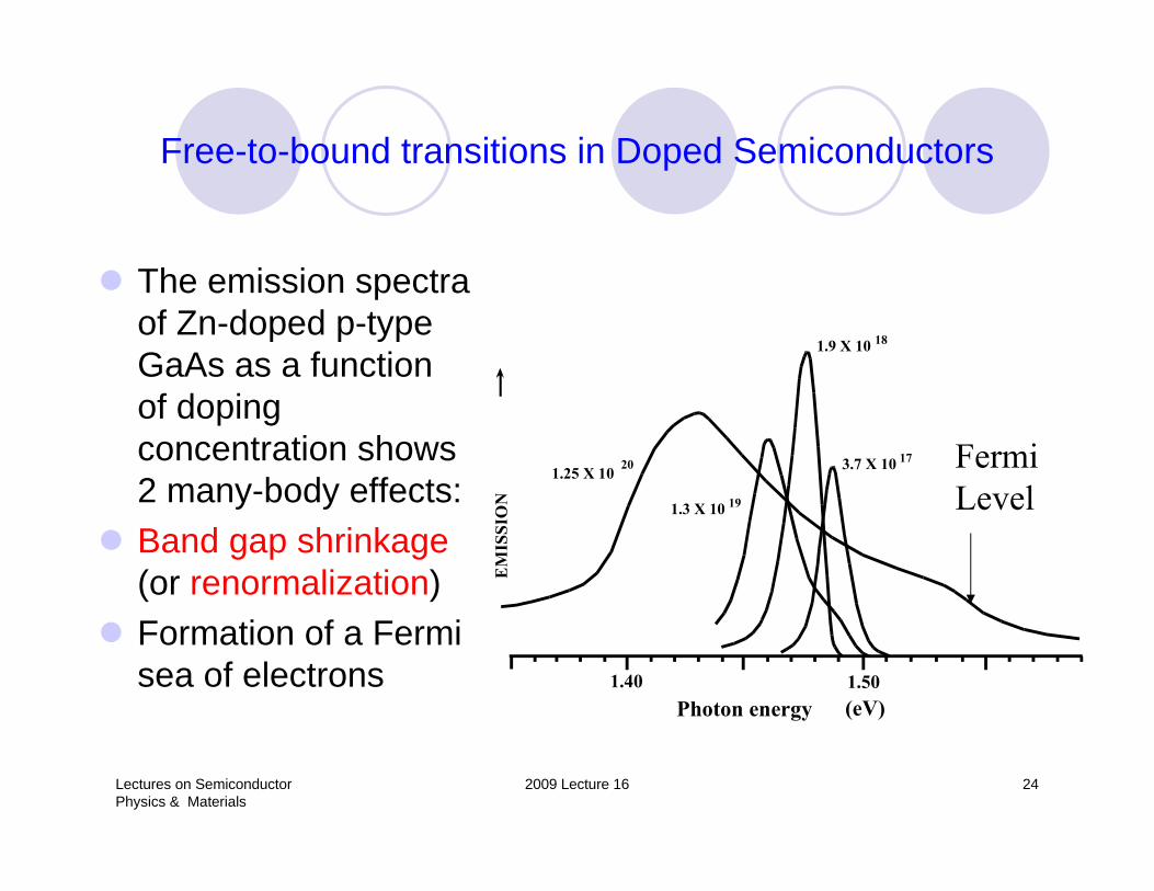
Free-to-bound transitions in Doped Semiconductors
The emission spectra of Zn-doped p-type GaAs as a function of doping concentration shows 2 many-body effects:Band gap shrinkage(or renormalization)Formation of a Fermi sea of electrons
1.25 X 10 20
1.3 X 10 19
3.7 X 10 17
1.9 X 10 18
1.40 1.50(eV)Photon energy
Fermi Level
Lectures on Semiconductor Physics & Materials
2009 Lecture 16 25
DAP transitionsIn a compensated semiconductor there are both donors and acceptorsRecombination of electrons at a donor with a hole at an acceptor exhibits also a final state interaction:
Do+Ao=>hω+ D++A-
Since the donor and acceptor becomes charged in the final state there is a Coulomb attraction between them. As a result the emitted photon energy hω is given by:hω =Eg-ED-EA+e2/(εoR)Where R= distance between donor and acceptor
Lectures on Semiconductor Physics & Materials
2009 Lecture 16 26
DAP transitions
Since the donors and acceptors can only sit on specific lattice sites R is discrete leading to sharp DAP linesThe position of the DAP lines depends on the lattice constant and on whether the donor and acceptor sit on the same sublattice (Type 1) or different sublattices (Type 2)
Lectures on Semiconductor Physics & Materials
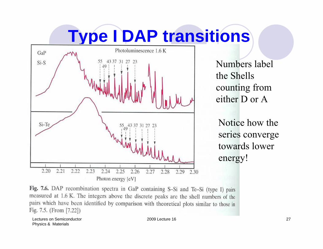
2009 Lecture 16 27
Type I DAP transitionsNumbers label the Shells counting from either D or A
Notice how the series converge towards lower energy!
Lectures on Semiconductor Physics & Materials
2009 Lecture 16 28
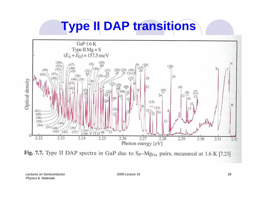
Type II DAP transitions
Lectures on Semiconductor Physics & Materials
2009 Lecture 16 29
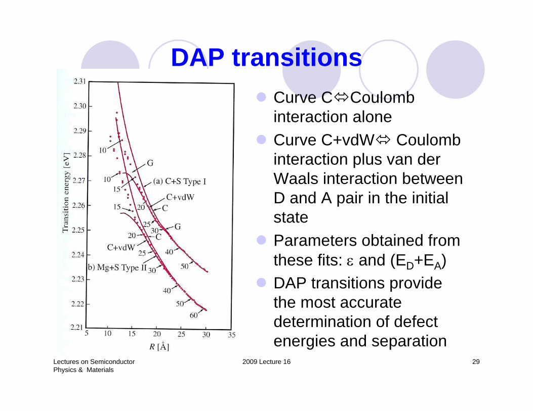
DAP transitionsCurve C Coulombinteraction aloneCurve C+vdW Coulomb interaction plus van derWaals interaction between D and A pair in the initial stateParameters obtained from these fits: ε and (ED+EA)DAP transitions provide the most accurate determination of defect energies and separation

![[Presentation (pdf, 4.2 Mb)] - Harvard Universityacmg.seas.harvard.edu/presentations/IGC6/talks/MonD_BC_curci... · SENSITIVITY TESTS WITH GEOS-Chem AEROSOL OPTICAL PROPERTIES: THE](https://static.fdocument.org/doc/165x107/5a9d74e07f8b9abd058d5ffa/presentation-pdf-42-mb-harvard-tests-with-geos-chem-aerosol-optical-properties.jpg)