
November - patonpublishinghouse.com · tions {v, u, T, φ), where v, u are the radial and axial...
46
E.O. Paton Electric Welding Institute of the National Academy of Sciences of Ukraine International Scientific-Technical and Production Journal November 2016 No. 11 Published since 2000 English translation of the monthly «Avtomaticheskaya Svarka» (Automatic Welding) journal published in Russian since 1948 EDITORIAL BOARD Editor-in-Chief B.E. Paton Scientists of PWI, Kiev S.I. Kuchuk-Yatsenko (vice-chief ed.), V.N. Lipodaev (vice-chief ed.), Yu.S. Borisov, G.M. Grigorenko, A.T. Zelnichenko, V.V. Knysh, I.V. Krivtsun, Yu.N. Lankin, L.M. Lobanov, V.D. Poznyakov, I.A. Ryabtsev, K.A. Yushchenko Scientists of Ukrainian Universities V.V. Dmitrik, NTU «KhPI», Kharkov V.V. Kvasnitsky, NTUU «KPl», Kiev V.D. Kuznetsov, NTUU «KPl», Kiev Foreign Scientists N.P. Alyoshin N.E. Bauman MSTU, Moscow, Russia Guan Qiao Beijing Aeronautical Institute, China A.S. Zubchenko DB «Gidropress», Podolsk, Russia M. Zinigrad Ariel University, Israel V.I. Lysak Volgograd STU, Russia Ya. Pilarczyk Welding Institute, Gliwice, Poland U. Reisgen Welding and Joining Institute, Aachen, Germany G.A. Turichin St. Petersburg SPU, Russia Founders E.O. Paton Electric Welding Institute, NASU International Association «Welding» Publisher International Association «Welding» Translators A.A. Fomin, O.S. Kurochko, I.N. Kutianova Editor N.G. Khomenko Electron galley D.I. Sereda, T.Yu. Snegiryova Address E.O. Paton Electric Welding Institute, International Association «Welding» 11 Kazimir Malevich Str. (former Bozhenko Str.), 03680, Kiev, Ukraine Tel.: (38044) 200 60 16, 200 82 77 Fax: (38044) 200 82 77, 200 81 45 E-mail: [email protected] www.patonpublishinghouse.com State Registration Certificate KV 4790 of 09.01.2001 ISSN 0957-798X Subscriptions $348, 12 issues per year, air postage and packaging included. Back issues available. All rights reserved. This publication and each of the articles contained herein are protected by copyright. Permission to reproduce material contained in this journal must be obtained in writing from the Publisher. © PWI, International Association «Welding», 2016 CONTENTS SCIENTIFIC AND TECHNICAL Krivtsun I.V., Krikent I.V. and Demchenko V.F. Numerical analysis of plasma characteristics of constricted and free-burning arc with a refractory cathode ......................................................................... 2 Grigorenko G.M., Akhonin S.V., Zadorozhnyuk O.M. and Klochkov I.N. Structure and properties of fully-penetrated metal of two-phase titanium alloy with dispersion hardening at AAW ....... 9 Babinets A.A., Ryabtsev I.A., Panfilov A.I., Zhdanov V.A. and Ryabtsev I.I. Influence of methods of arc surfacing with flux-cored wire on penetration of base metal and formation of deposited metal ................................................................................................ 17 Zhemanyuk P.D., Petrik I.A., Chigilejchik S.L., Yarovitsyn A.V. and Khrushchov G.D. Peculiarities of bead shape regulation in single-layer microplasma surfacing on edges of aircraft gas turbine engine blades ...................................................................... 23 Khaskin V.Yu., Korzhik V.N., Chizhskaya T.G., Sidorets V.N. and Lo Zie. Effect of laser radiation absorption on efficiency of laser welding of copper and its alloys .......................................... 31 INDUSTRIAL Lankin Yu.N. and Soloviov V.G. Information-measuring system for arc welding and surfacing ........................................................... 36 Burlaka V.V. and Gulakov S.V. Device for excitation and stabilization of welding arc ............................................................... 43
Transcript of November - patonpublishinghouse.com · tions {v, u, T, φ), where v, u are the radial and axial...
E.O. Paton E lec t r i c Weld ing Ins t i tu te o f the Nat iona l Academy o f Sc iences o f Ukra ine
International Scientific-Technical and Production JournalNovember 2016
No. 11Published since 2000
English translation of the monthly «Avtomaticheskaya Svarka» (Automatic Welding) journal published in Russian since 1948
EDITORIAL BOARD
Editor-in-Chief B.E. Paton
Scientists of PWI, Kiev S.I. Kuchuk-Yatsenko (vice-chief ed.),
V.N. Lipodaev (vice-chief ed.), Yu.S. Borisov, G.M. Grigorenko,
A.T. Zelnichenko, V.V. Knysh, I.V. Krivtsun, Yu.N. Lankin,
L.M. Lobanov, V.D. Poznyakov, I.A. Ryabtsev, K.A. Yushchenko
Scientists of Ukrainian Universities V.V. Dmitrik, NTU «KhPI», Kharkov V.V. Kvasnitsky, NTUU «KPl», Kiev V.D. Kuznetsov, NTUU «KPl», Kiev
Foreign Scientists N.P. Alyoshin
N.E. Bauman MSTU, Moscow, Russia Guan Qiao
Beijing Aeronautical Institute, China A.S. Zubchenko
DB «Gidropress», Podolsk, Russia M. Zinigrad
Ariel University, Israel V.I. Lysak
Volgograd STU, Russia Ya. Pilarczyk
Welding Institute, Gliwice, Poland U. Reisgen
Welding and Joining Institute, Aachen, Germany G.A. Turichin
St. Petersburg SPU, Russia
Founders E.O. Paton Electric Welding Institute, NASU
International Association «Welding»Publisher
International Association «Welding»Translators
A.A. Fomin, O.S. Kurochko, I.N. Kutianova Editor
N.G. Khomenko Electron galley
D.I. Sereda, T.Yu. SnegiryovaAddress
E.O. Paton Electric Welding Institute, International Association «Welding»
11 Kazimir Malevich Str. (former Bozhenko Str.), 03680, Kiev, Ukraine
Tel.: (38044) 200 60 16, 200 82 77 Fax: (38044) 200 82 77, 200 81 45
E-mail: [email protected] www.patonpublishinghouse.com
State Registration Certificate
KV 4790 of 09.01.2001 ISSN 0957-798XSubscriptions
$348, 12 issues per year, air postage and packaging included.
Back issues available.All rights reserved.
This publication and each of the articles contained herein are protected by copyright.
Permission to reproduce material contained in this journal must be obtained in writing from the Publisher.
© PWI, International Association «Welding», 2016
C O N T E N T S
SCIENTIFIC AND TECHNICAL
Krivtsun I.V., Krikent I.V. and Demchenko V.F. Numerical analysis of plasma characteristics of constricted and free-burning arc with a refractory cathode ......................................................................... 2
Grigorenko G.M., Akhonin S.V., Zadorozhnyuk O.M. and Klochkov I.N. Structure and properties of fully-penetrated metal of two-phase titanium alloy with dispersion hardening at AAW ....... 9
Babinets A.A., Ryabtsev I.A., Panfilov A.I., Zhdanov V.A. and Ryabtsev I.I. Influence of methods of arc surfacing with flux-cored wire on penetration of base metal and formation of deposited metal ................................................................................................ 17
Zhemanyuk P.D., Petrik I.A., Chigilejchik S.L., Yarovitsyn A.V. and Khrushchov G.D. Peculiarities of bead shape regulation in single-layer microplasma surfacing on edges of aircraft gas turbine engine blades ...................................................................... 23
Khaskin V.Yu., Korzhik V.N., Chizhskaya T.G., Sidorets V.N. and Lo Zie. Effect of laser radiation absorption on efficiency of laser welding of copper and its alloys .......................................... 31
INDUSTRIAL
Lankin Yu.N. and Soloviov V.G. Information-measuring system for arc welding and surfacing ........................................................... 36
Burlaka V.V. and Gulakov S.V. Device for excitation and stabilization of welding arc ............................................................... 43
2 ISSN 0957-798X THE PATON WELDING JOURNAL, No. 11, 2016
SCIENTIFIC AND TECHNICAL
doi.org/10.15407/tpwj2016.11.01
NUMERICAL ANALYSIS OF PLASMA CHARACTERISTICS OF CONSTRICTED AND FREE-BURNING ARC
WITH A REFRACTORY CATHODE*
I.V. KRIVTSUN1, I.V. KRIKENT2 and V.F. DEMCHENKO1
1E.O. Paton Electric Welding Institute, NASU 11 Kazimir Malevich Str., 03680, Kiev, Ukraine. E-mail: [email protected]
2Dnieprodzerzhinsk State Technical University 2 Dnieprostrojevskaya Str., 51918, Dnieprodzerzhinsk, Ukraine
Self-consistent mathematical model of the processes of energy-, mass- and electric transfer in the column and anode region of the electric arc with refractory cathode was used as a basis to perform numerical analysis of thermal, elec-tromagnetic and gas-dynamic characteristics of arc plasma for constricted (plasma) and free-burning argon arc with copper water-cooled anode. Results of calculation of characteristics of arc column plasma show that distributions of electric current density, temperature and velocity of constricted arc plasma can greatly differ from the respective distributions for free-burning arc, depending on arc current, plasmatron nozzle channel diameter and plasma gas flow rate. Characteristics of near-anode layer of plasma arc also differ significantly from the respective characteristics of free-burning arc, depending on the above arcing mode parameters. Thus, by varying arc current, plasmatron nozzle channel diameter and plasma gas flow rate, it is possible to effectively control the characteristics of thermal, electro-magnetic and, particularly, dynamic impact of the constricted arc on anode metal surface. 13 Ref., 1 Table, 10 Figures.
K e y w o r d s : constricted (plasma) arc, free-burning arc, refractory cathode, water-cooled anode, arc column, anode region, arc plasma characteristics, mathematical modeling
Application of a constricted (plasma) arc instead of free-burning one is one of the methods to improve the effectiveness of electric arc impact on metals, and, consequently, to increase the penetration depth and nonconsumable electrode welding speed. Lim-itation of transverse dimensions of the column of an arc with refractory cathode by the wall of plasmatron nozzle channel can lead to an essential increase of the density of electric current and heat flow, applied by the arc to the metal being welded, and variation of plasma gas flow rate enables varying in a broad range the dynamic impact of arc plasma flow on weld pool surface. Effective practical application of plasma arc as welding heat source requires having valid infor-mation on distributed characteristics of constricted arc plasma, as well as characteristics of its thermal, electromagnetic and gas-dynamic impact on the met-al being welded. As experimental determination of such, important in practical terms, plasma arc char-acteristics as distribution of electric current density, heat flow and gas-dynamic pressure of plasma over the weld pool surface is difficult, because of high val-ues of arc plasma temperature and temperature of the above-mentioned surface, smallness of geometrical dimensions of the arc anode region and a number of
other factors, studying the plasma arc by mathemati-cal modeling methods seems highly relevant (see, for instance, [1–6]). Therefore, the objective of this work is detailed numerical analysis of distributed charac-teristics of plasma column and anode region of the constricted arc, depending on its arcing mode, as well as their comparison with the respective characteristics for a free-burning arc.
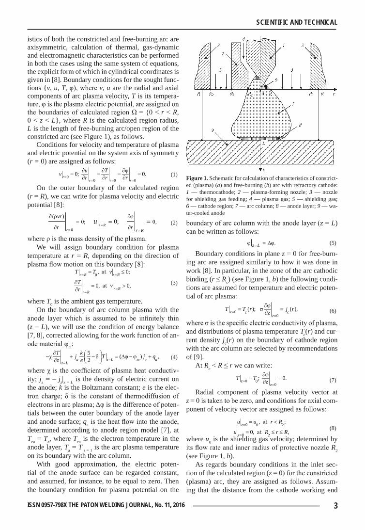
Let us consider a stationary electric arc with a re-fractory cathode (W) and water-cooled (non-evapo-rating) anode (Cu), burning in an argon flow at atmo-spheric pressure. We will study two variants — plasma arc, constricted by the wall of the cylindrical channel of plasmatron nozzle (Figure 1, a), and free-burning arc (Figure 1, b). At selection of mathematical model of arc plasma, we will assume that arc column plasma in both the cases is isothermal and single-component, containing only particles of shielding or plasma gas (Ar). Numerical analysis of such plasma characteris-tics can be performed using a self-consistent math-ematical model of processes of energy-, mass-, and electric transfer in the column and anode region of the welding arc, proposed in [7], and reduced allowing for the above assumptions, as described in [8]. As-suming further that distributions of plasma character-
*Basing on the paper presented at the VIII International Conference on Mathematical Modelling and Information Technologies in Welding and Related Processes (Sept. 18–23, 2016, Odessa, Ukraine).
© I.V. KRIVTSUN, I.V. KRIKENT and V.F. DEMCHENKO, 2016
3ISSN 0957-798X THE PATON WELDING JOURNAL, No. 11, 2016
SCIENTIFIC AND TECHNICAL
istics of both the constricted and free-burning arc are axisymmetric, calculation of thermal, gas-dynamic and electromagnetic characteristics can be performed in both the cases using the same system of equations, the explicit form of which in cylindrical coordinates is given in [8]. Boundary conditions for the sought func-tions {v, u, T, φ), where v, u are the radial and axial components of arc plasma velocity, T is its tempera-ture, φ is the plasma electric potential, are assigned on the boundaries of calculated region Ω = {0 < r < R, 0 < z < L}, where R is the calculated region radius, L is the length of free-burning arc/open region of the constricted arc (see Figure 1), as follows.
Conditions for velocity and temperature of plasma and electric potential on the system axis of symmetry (r = 0) are assigned as follows:
0
0 0 00; 0.r
r r r
u Tv r r r== = =
∂ ∂ ∂ϕ= = = =
∂ ∂ ∂ (1)
On the outer boundary of the calculated region (r = R), we can write for plasma velocity and electric potential [8]:
( )0; 0,0;
r Rr R r R
vr
r ru
== =
∂ ρ ∂ϕ=
∂ ∂= =
(2)
where ρ is the mass density of the plasma.We will assign boundary condition for plasma
temperature at r = R, depending on the direction of plasma flow motion on this boundary [8]:
0 , 0;
0, 0,
at
at
r R r R
r Rr R
T T v
T vr
= =
==
= ≤
∂= >
∂
(3)
where T0 is the ambient gas temperature.On the boundary of arc column plasma with the
anode layer which is assumed to be infinitely thin (z = L), we will use the condition of energy balance [7, 8], corrected allowing for the work function of an-ode material φm:
5 ( ) ,2 z La m a az L
T kj T j qz e ==
∂ −χ + − d = Dϕ − ϕ + ∂ (4)
where χ is the coefficient of plasma heat conductiv-ity; ja = – jz|z = L is the density of electric current on the anode; k is the Boltzmann constant; e is the elec-tron charge; δ is the constant of thermodiffusion of electrons in arc plasma; Δφ is the difference of poten-tials between the outer boundary of the anode layer and anode surface; qa is the heat flow into the anode, determined according to anode region model [7], at Tea = Ta, where Tea is the electron temperature in the anode layer, Ta = T|z = 1 is the arc plasma temperature on its boundary with the arc column.
With good approximation, the electric poten-tial of the anode surface can be regarded constant, and assumed, for instance, to be equal to zero. Then the boundary condition for plasma potential on the
boundary of arc column with the anode layer (z = L) can be written as follows:
.z L=ϕ = Dϕ
(5)
Boundary conditions in plane z = 0 for free-burn-ing arc are assigned similarly to how it was done in work [8]. In particular, in the zone of the arc cathodic binding (r ≤ Rc) (see Figure 1, b) the following condi-tions are assumed for temperature and electric poten-tial of arc plasma:
0
0( ); ( ),z c c
zT T r j rz=
=
∂ϕ= s =
∂ (6)
where σ is the specific electric conductivity of plasma, and distributions of plasma temperature Tc(r) and cur-rent density jc(r) on the boundary of cathode region with the arc column are selected by recommendations of [9].
At Rc < R ≤ r we can write:
0 0
0; 0.z
zT T z=
=
∂ϕ= =
∂ (7)
Radial component of plasma velocity vector at z = 0 is taken to be zero, and conditions for axial com-ponent of velocity vector are assigned as follows:
0 0 2
0 2
, ;
0, ,
at
atz
z
u u r R
u R r R=
=
= <
= ≤ ≤
(8)
where u0 is the shielding gas velocity; determined by its flow rate and inner radius of protective nozzle R2 (see Figure 1, b).
As regards boundary conditions in the inlet sec-tion of the calculated region (z = 0) for the constricted (plasma) arc, they are assigned as follows. Assum-ing that the distance from the cathode working end
Figure 1. Schematic for calculation of characteristics of constrict-ed (plasma) (a) and free-burning (b) arc with refractory cathode: 1 — thermocathode; 2 — plasma-forming nozzle; 3 — nozzle for shielding gas feeding; 4 — plasma gas; 5 — shielding gas; 6 — cathode region; 7 — arc column; 8 — anode layer; 9 — wa-ter-cooled anode
4 ISSN 0957-798X THE PATON WELDING JOURNAL, No. 11, 2016
SCIENTIFIC AND TECHNICAL
to plasmaforming channel edge (see Figure 1, a) is essentially larger than its radius Rp, it can be taken that a one-dimensional flow of arc plasma (in the di-rection of OZ axis) is in place at the channel outlet, its temperature and velocity depending only on the radial coordinate; radial components of plasma velocity and electric field intensity are equal to zero, and pressure gradient dp/dz and axial component of electric field Ez are constant across the channel section [1]. In this case, distributions of temperature T(r) and axial component of plasma velocity u(r) on the channel edge (r ≤ Rp) are found by solving one-dimensional equations:
21 0;z
d dTr Er dr dr
χ + s −ψ =
(9)
1 0.dpd durr dr dr dz
h − =
(10)
Here, ψ are the losses of plasma energy for radi-ation; η is the coefficient of plasma dynamic viscos-ity, and the value of axial component of electric field (electric potential gradient) Ez = –(dφ/dz) and pressure gradient dp/dz are found from integral relationships:
0 02 ; 2 ,
p p
z
R RI E rdr G urdr= s = p ρ∫ ∫
(11)
where I is the arc current; G is the mass flow of plas-ma gas.
Boundary conditions for equations (9), (10) are se-lected in keeping with the conditions of flow symme-try (1) and conditions of «sticking» on the cooled wall of plasma-forming channel that yields:
0 0
0
, 0;
.0,;
at
atp
r r
R
T u rr r
TT u r= =
∂ ∂= =
∂ ∂
= ==
(12)
At Rr < r ≤ R boundary conditions for temperature and electric potential coincide with (7), radial compo-nent of plasma velocity vector is assumed to be zero, and conditions for axial component of velocity are as-signed as follows:
0 1
0 0 1 2
0 2
0, ;
, ;
0, ,
at
at
at
z p
z
z
u R r R
u u R r R
u R r R
=
=
=
= ≤ ≤
= < <
= ≤ ≤
(13)
where u0 is the shielding gas velocity in the case of a constricted arc, determined by its flow rate, as well as inner R1 and outer R2 radii of the nozzle for its feeding (see Figure 1, a).
Initial system of equations [8], together with bound-ary conditions (1)–(8) for free-burning arc and (1)–(5), (9)–(13) for plasma arc, was solved numerically, by finite difference method. Temperature dependencies of thermodynamic properties, transport coefficients and emissivity of arc plasma were determined using calculated data for isothermal argon plasma of atmo-spheric pressure, given in [10]. At numerical solution of gas-dynamic and heat problems, joint Lagrangian–
Euler method was used [11, 12], which was adapted to the conditions of the compressible medium.
Comparative numerical analysis of arc plasma characteristics, as well as characteristics of its ther-mal, electromagnetic and gas-dynamic impact on the anode surface for constricted (plasma) arc and free-burning arc, was performed at the following pa-rameters: arc current I = 100, 150, 200 A; length of free-burning arc/length of plasma arc open region L = = 3 mm; diameter of plasmatron nozzle channel d = = 2Rp = 2, 3, 4 mm; mass flow of plasma gas (Ar) was varied in the range of G = 0.10–0.75∙10–4 kg/s, that corresponds to volume flow of 0.34–2.55 l/min. In the case of plasma arc, the inner and outer radii of annular nozzle for feeding the shielding gas (Ar) Ri = 4.4 mm, R2 = 7.7 mm (see Figure 1, a); shielding gas rate u0 = = 0.65 m/s. In the case of free-burning arc R2 = 7.7 mm (see Figure 1, b); u0 = 0.5 m/s. In both the cases, the radius of calculated region R was selected equal to 8 mm; temperature of water-cooled anode surface, temperature of plasma-forming and protective nozzle walls, as well as temperature of the fed shielding gas T0 was taken to be equal to 500 K.
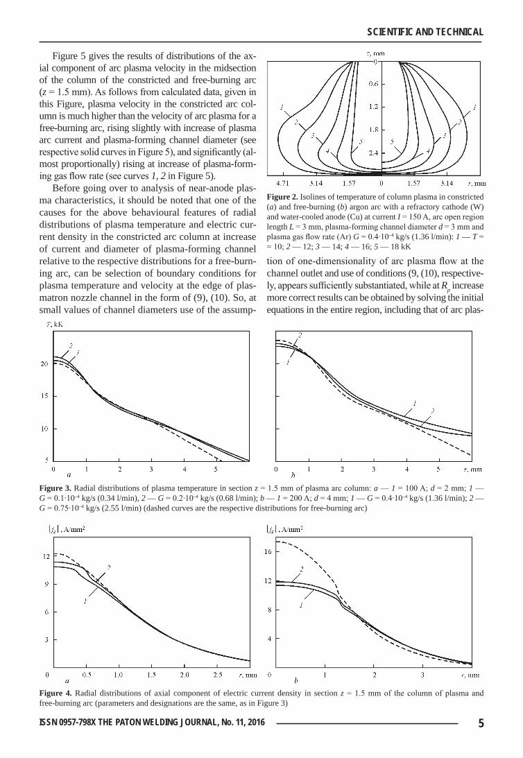
Figure 2 gives the isolines of plasma temperature in the column of constricted (see Figure 2, a) and free-burning arc (see Figure 2, b). As follows from calculated data presented in this Figure, constriction of plasma arc initial region by the wall of the channel blown by plasma gas flow, leads to a certain elongation of the isotherms along the arc axis and to increase of the length of the column high-temperature region (T ≥ ≥ 16000 K), compared to free-burning arc. As regards radial distributions of arc plasma temperature, in the case of 100 ampere arc, formed by a plasmatron with nozzle channel diameter of 2 mm, the temperature in the column center turns out to be somewhat higher than the respective temperature for a free-burning arc, rising insignificantly with increase of plasma gas flow (Figure 3, a). For the case of I = 200 A, d = 4 mm, the temperature in plasma arc center turns out to be a little lower than that for a free-burning arc (at preservation of the tendency to slight increase of axial value with G increase, shown in Figure 3, b), that is indicative of weakening of the effect of arc column constriction at the respective increase of current and diameter of plasmaforming channel.
A more clearly marked feature appears in calculat-ed distributions of electric current density in the arc column, given in Figure 4. In both the considered cas-es current density in the center of plasma arc column turns out to be lower than the respective values for a free-burning arc (see Figure 4). An important circum-stance here is the change of the nature of radial dis-tribution of value |jz| for a constricted arc, compared with the free-burning one, namely, appearance of a «plateau» in the respective distributions near the col-umn axis (see solid curves in Figure 4).
5ISSN 0957-798X THE PATON WELDING JOURNAL, No. 11, 2016
SCIENTIFIC AND TECHNICAL
Figure 5 gives the results of distributions of the ax-ial component of arc plasma velocity in the midsection of the column of the constricted and free-burning arc (z = 1.5 mm). As follows from calculated data, given in this Figure, plasma velocity in the constricted arc col-umn is much higher than the velocity of arc plasma for a free-burning arc, rising slightly with increase of plasma arc current and plasma-forming channel diameter (see respective solid curves in Figure 5), and significantly (al-most proportionally) rising at increase of plasma-form-ing gas flow rate (see curves 1, 2 in Figure 5).
Before going over to analysis of near-anode plas-ma characteristics, it should be noted that one of the causes for the above behavioural features of radial distributions of plasma temperature and electric cur-rent density in the constricted arc column at increase of current and diameter of plasma-forming channel relative to the respective distributions for a free-burn-ing arc, can be selection of boundary conditions for plasma temperature and velocity at the edge of plas-matron nozzle channel in the form of (9), (10). So, at small values of channel diameters use of the assump-
tion of one-dimensionality of arc plasma flow at the channel outlet and use of conditions (9, (10), respective-ly, appears sufficiently substantiated, while at Rp increase more correct results can be obtained by solving the initial equations in the entire region, including that of arc plas-
Figure 2. Isolines of temperature of column plasma in constricted (a) and free-burning (b) argon arc with a refractory cathode (W) and water-cooled anode (Cu) at current I = 150 A, arc open region length L = 3 mm, plasma-forming channel diameter d = 3 mm and plasma gas flow rate (Ar) G = 0.4∙10–4 kg/s (1.36 l/min): 1 — T = = 10; 2 — 12; 3 — 14; 4 — 16; 5 — 18 kK
Figure 3. Radial distributions of plasma temperature in section z = 1.5 mm of plasma arc column: a — 1 = 100 A; d = 2 mm; 1 — G = 0.1∙10–4 kg/s (0.34 l/min), 2 — G = 0.2∙10–4 kg/s (0.68 l/min); b — 1 = 200 A; d = 4 mm; 1 — G = 0.4∙10–4 kg/s (1.36 l/min); 2 — G = 0.75∙10–4 kg/s (2.55 l/min) (dashed curves are the respective distributions for free-burning arc)
Figure 4. Radial distributions of axial component of electric current density in section z = 1.5 mm of the column of plasma and free-burning arc (parameters and designations are the same, as in Figure 3)
6 ISSN 0957-798X THE PATON WELDING JOURNAL, No. 11, 2016
SCIENTIFIC AND TECHNICAL
ma inside the plasmatron nozzle channel (see Figure 1, a), that we intend to do at the next research stage.
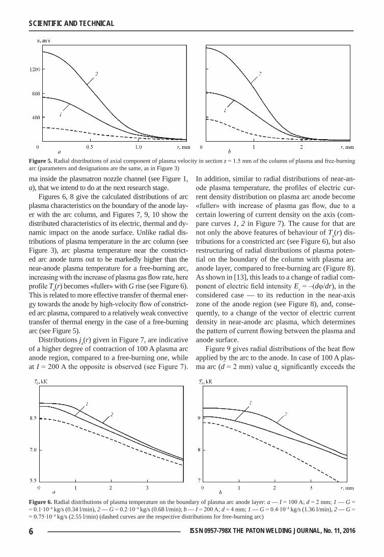
Figures 6, 8 give the calculated distributions of arc plasma characteristics on the boundary of the anode lay-er with the arc column, and Figures 7, 9, 10 show the distributed characteristics of its electric, thermal and dy-namic impact on the anode surface. Unlike radial dis-tributions of plasma temperature in the arc column (see Figure 3), arc plasma temperature near the constrict-ed arc anode turns out to be markedly higher than the near-anode plasma temperature for a free-burning arc, increasing with the increase of plasma gas flow rate, here profile Ta(r) becomes «fuller» with G rise (see Figure 6). This is related to more effective transfer of thermal ener-gy towards the anode by high-velocity flow of constrict-ed arc plasma, compared to a relatively weak convective transfer of thermal energy in the case of a free-burning arc (see Figure 5).
Distributions ja(r) given in Figure 7, are indicative of a higher degree of contraction of 100 A plasma arc anode region, compared to a free-burning one, while at I = 200 A the opposite is observed (see Figure 7).
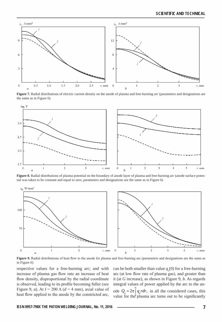
In addition, similar to radial distributions of near-an-ode plasma temperature, the profiles of electric cur-rent density distribution on plasma arc anode become «fuller» with increase of plasma gas flow, due to a certain lowering of current density on the axis (com-pare curves 1, 2 in Figure 7). The cause for that are not only the above features of behaviour of Ta(r) dis-tributions for a constricted arc (see Figure 6), but also restructuring of radial distributions of plasma poten-tial on the boundary of the column with plasma arc anode layer, compared to free-burning arc (Figure 8). As shown in [13], this leads to a change of radial com-ponent of electric field intensity Er = –(dφ/dr), in the considered case — to its reduction in the near-axis zone of the anode region (see Figure 8), and, conse-quently, to a change of the vector of electric current density in near-anode arc plasma, which determines the pattern of current flowing between the plasma and anode surface.
Figure 9 gives radial distributions of the heat flow applied by the arc to the anode. In case of 100 A plas-ma arc (d = 2 mm) value qa significantly exceeds the
Figure 5. Radial distributions of axial component of plasma velocity in section z = 1.5 mm of the column of plasma and free-burning arc (parameters and designations are the same, as in Figure 3)
Figure 6. Radial distributions of plasma temperature on the boundary of plasma arc anode layer: a — I = 100 A; d = 2 mm; 1 — G = = 0.1∙10–4 kg/s (0.34 l/min), 2 — G = 0.2∙10–4 kg/s (0.68 l/min); b — I = 200 A; d = 4 mm; 1 — G = 0.4∙10–4 kg/s (1.36 l/min), 2 — G = = 0.75∙10–4 kg/s (2.55 l/min) (dashed curves are the respective distributions for free-burning arc)
7ISSN 0957-798X THE PATON WELDING JOURNAL, No. 11, 2016
SCIENTIFIC AND TECHNICAL
respective values for a free-burning arc; and with increase of plasma gas flow rate an increase of heat flow density, disproportional by the radial coordinate is observed, leading to its profile becoming fuller (see Figure 9, a). At I = 200 A (d = 4 mm), axial value of heat flow applied to the anode by the constricted arc,
can be both smaller than value qa(0) for a free-burning arc (at low flow rate of plasma gas), and greater than it (at G increase), as shown in Figure 9, b. As regards integral values of power applied by the arc to the an-ode
02 ,a aQ q rdr
∞= p∫ in all the considered cases, this
value for the plasma arc turns out to be significantly
Figure 7. Radial distributions of electric current density on the anode of plasma and free-burning arc (parameters and designations are the same as in Figure 6)
Figure 8. Radial distributions of plasma potential on the boundary of anode layer of plasma and free-burning arc (anode surface poten-tial was taken to be constant and equal to zero, parameters and designations are the same as in Figure 6)
Figure 9. Radial distributions of heat flow to the anode for plasma and free-burning arc (parameters and designations are the same as in Figure 6)
8 ISSN 0957-798X THE PATON WELDING JOURNAL, No. 11, 2016
SCIENTIFIC AND TECHNICAL
higher than that for a free-burning one, and it rises with increase of plasma gas flow rate, as follows from calculated data given in the Table. The main cause for that is intensive transfer of thermal energy from the high-temperature region of the constricted arc column towards the anode, performed by a higher-velocity flow of arc plasma, than in the case of a free-burning arc (see Figure 5).
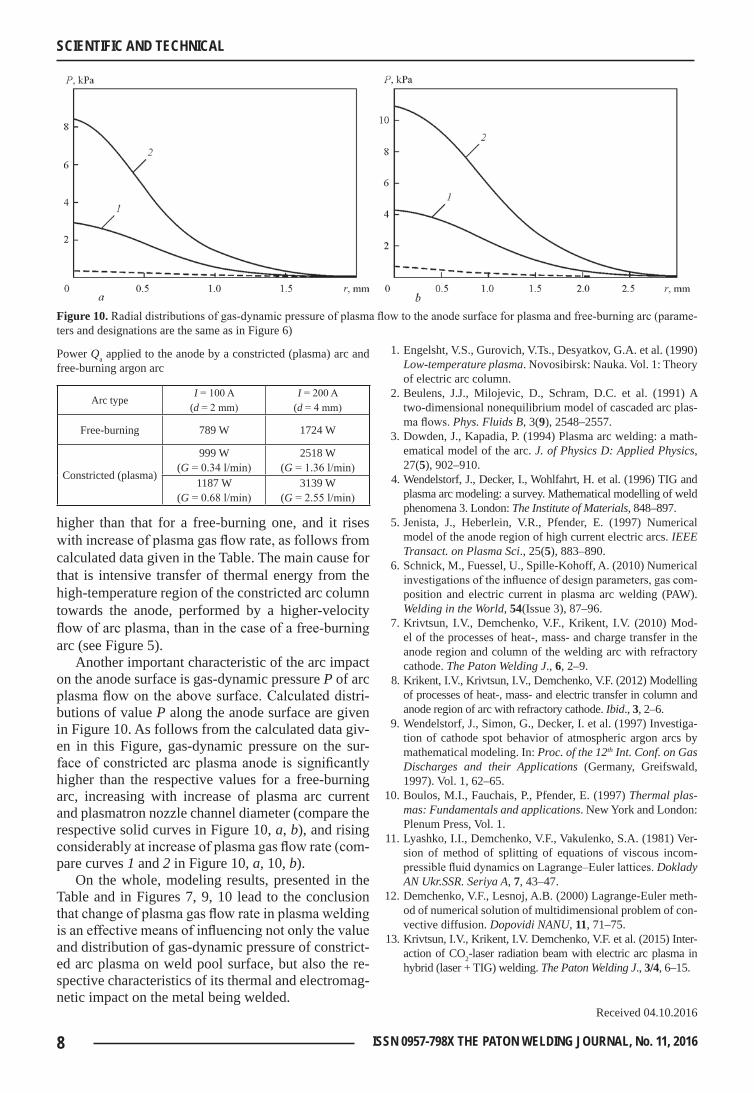
Another important characteristic of the arc impact on the anode surface is gas-dynamic pressure P of arc plasma flow on the above surface. Calculated distri-butions of value P along the anode surface are given in Figure 10. As follows from the calculated data giv-en in this Figure, gas-dynamic pressure on the sur-face of constricted arc plasma anode is significantly higher than the respective values for a free-burning arc, increasing with increase of plasma arc current and plasmatron nozzle channel diameter (compare the respective solid curves in Figure 10, a, b), and rising considerably at increase of plasma gas flow rate (com-pare curves 1 and 2 in Figure 10, a, 10, b).
On the whole, modeling results, presented in the Table and in Figures 7, 9, 10 lead to the conclusion that change of plasma gas flow rate in plasma welding is an effective means of influencing not only the value and distribution of gas-dynamic pressure of constrict-ed arc plasma on weld pool surface, but also the re-spective characteristics of its thermal and electromag-netic impact on the metal being welded.
1. Engelsht, V.S., Gurovich, V.Ts., Desyatkov, G.A. et al. (1990) Low-temperature plasma. Novosibirsk: Nauka. Vol. 1: Theory of electric arc column.
2. Beulens, J.J., Milojevic, D., Schram, D.C. et al. (1991) A two-dimensional nonequilibrium model of cascaded arc plas-ma flows. Phys. Fluids B, 3(9), 2548–2557.
3. Dowden, J., Kapadia, P. (1994) Plasma arc welding: a math-ematical model of the arc. J. of Physics D: Applied Physics, 27(5), 902–910.
4. Wendelstorf, J., Decker, I., Wohlfahrt, H. et al. (1996) TIG and plasma arc modeling: a survey. Mathematical modelling of weld phenomena 3. London: The Institute of Materials, 848–897.
5. Jenista, J., Heberlein, V.R., Pfender, E. (1997) Numerical model of the anode region of high current electric arcs. IEEE Transact. on Plasma Sci., 25(5), 883–890.
6. Schnick, M., Fuessel, U., Spille-Kohoff, A. (2010) Numerical investigations of the influence of design parameters, gas com-position and electric current in plasma arc welding (PAW). Welding in the World, 54(Issue 3), 87–96.
7. Krivtsun, I.V., Demchenko, V.F., Krikent, I.V. (2010) Mod-el of the processes of heat-, mass- and charge transfer in the anode region and column of the welding arc with refractory cathode. The Paton Welding J., 6, 2–9.
8. Krikent, I.V., Krivtsun, I.V., Demchenko, V.F. (2012) Modelling of processes of heat-, mass- and electric transfer in column and anode region of arc with refractory cathode. Ibid., 3, 2–6.
9. Wendelstorf, J., Simon, G., Decker, I. et al. (1997) Investiga-tion of cathode spot behavior of atmospheric argon arcs by mathematical modeling. In: Proc. of the 12th Int. Conf. on Gas Discharges and their Applications (Germany, Greifswald, 1997). Vol. 1, 62–65.
10. Boulos, M.I., Fauchais, P., Pfender, E. (1997) Thermal plas-mas: Fundamentals and applications. New York and London: Plenum Press, Vol. 1.
11. Lyashko, I.I., Demchenko, V.F., Vakulenko, S.A. (1981) Ver-sion of method of splitting of equations of viscous incom-pressible fluid dynamics on Lagrange–Euler lattices. Doklady AN Ukr.SSR. Seriya A, 7, 43–47.
12. Demchenko, V.F., Lesnoj, A.B. (2000) Lagrange-Euler meth-od of numerical solution of multidimensional problem of con-vective diffusion. Dopovidi NANU, 11, 71–75.
13. Krivtsun, I.V., Krikent, I.V. Demchenko, V.F. et al. (2015) Inter-action of CO2-laser radiation beam with electric arc plasma in hybrid (laser + TIG) welding. The Paton Welding J., 3/4, 6–15.
Received 04.10.2016
Figure 10. Radial distributions of gas-dynamic pressure of plasma flow to the anode surface for plasma and free-burning arc (parame-ters and designations are the same as in Figure 6)
Power Qa applied to the anode by a constricted (plasma) arc and free-burning argon arc
Arc typeI = 100 A
(d = 2 mm)I = 200 A
(d = 4 mm)
Free-burning 789 W 1724 W
Constricted (plasma)
999 W (G = 0.34 l/min)
2518 W (G = 1.36 l/min)
1187 W (G = 0.68 l/min)
3139 W (G = 2.55 l/min)
9ISSN 0957-798X THE PATON WELDING JOURNAL, No. 11, 2016
SCIENTIFIC AND TECHNICAL
doi.org/10.15407/tpwj2016.11.02
STRUCTURE AND PROPERTIES OF FULLY-PENETRATED METAL
OF TWO-PHASE TITANIUM ALLOY WITH DISPERSION HARDENING AT AAW
G.M. GRIGORENKO, S.V. AKHONIN, O.M. ZADOROZHNYUK and I.N. KLOCHKOVE.O. Paton Electric Welding Institute, NASU
11 Kazimir Malevich Str., 03680, Kiev, Ukraine. E-mail: [email protected]
Tungsten inert gas welding remains the most widespread, relatively easy and versatile method for manufacture of the structures of titanium alloys. Welding can be performed in different spatial positions and equipment can be sufficient-ly fast readjusted at change of joint type and thickness of metal being welded. Aim of present work lies in study and comparison of a structure and mechanical properties of fully-penetrated metal of high-strength titanium alloys with dispersion hardening and without it, produced using argon-arc method. It is shown that in comparison with titanium alloy VT23 an experimental dispersion-hardened alloy has higher strength indices of fully-penetrated metal, however ductility and impact toughness are extremely low, therefore this type of welding and heat treatment is not recommended for it. 11 Ref., 6 Tables, 16 Figures.
K e y w o r d s : argon-arc welding, TIG, structure, dispersion hardening, titanium silicides, mechanical properties, heat treatment
Structural high-strength titanium-based alloys due to their unique characteristics, such as high specific strength at keeping satisfactory ductility and high cor-rosion resistance, have found wide application in air-craft and rocket construction as well as gas-turbine en-gine production. Thus, for example, a frame design of modern passenger aircrafts has by mass around 15 % of complexly-alloyed titanium alloys and that for mil-itary aircrafts makes up to 40 %. Further development of aircraft and rocket engineering requires significant increase of service properties of titanium alloys. One of the ways to rise the ultimate strength of such alloys is dispersion hardening of metal due to precipitation of disperse particles from solid solution [1–5].
Tungsten inert gas welding is still one of the most widespread, relatively easy and versatile methods for manufacture of the structures of titanium alloys [6].
In addition to experimental (a + b)-alloy (close on composition to known Ti-1008 [7] (Table 1), the in-vestigations were also carried out on structure, phase composition and mechanical properties of argon-arc welded joints of commercial high-strength alloy VT23. It is medium (a + b)-alloy of martensite class, which transfers from b-phase to martensite form after quenching. This alloy differs from other by increased process ductility that allows using rolling, milling, drawing, stamping, flanging and other operations, re-lated with shaping in process of part manufacture [8].
Rise of alloy doping level promotes for increase of their sensitivity to welding thermal cycle and danger
of welded joint brittle fracture due to reduced ductili-ty. Two-phase titanium (a + b)-alloys considerably in-crease strength characteristics after aging and quench-ing. However, high strength of these alloys, with few exceptions, is impossible to realize in the welded structures, that is caused by difficulties, appearing in process of quenching and aging of the structures, and specifically by reduced ductility of welded joints in thermally-hardened state [9].
Aim of this investigation lies in study of effect of TIG welding method on weldability of titanium alloys with dispersion hardening. The results of examination of structure, phase composition and mechanical prop-erties of pilot alloy base metal are described in details in work [7].
Welding heating was carried out by tungsten non-consumable electrode (no filler wire) without full penetration of metal. Welding current made 350 A, welding rate was 10 m/h and 12 V arc voltage.
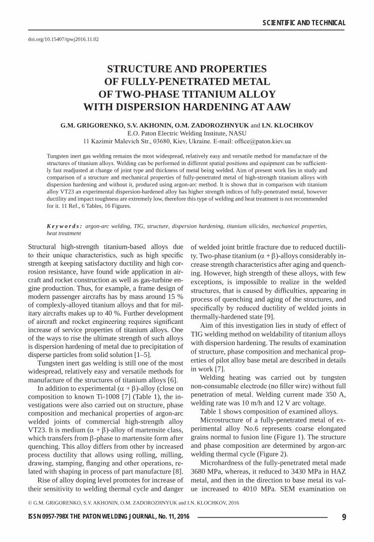
Table 1 shows composition of examined alloys.Microstructure of a fully-penetrated metal of ex-
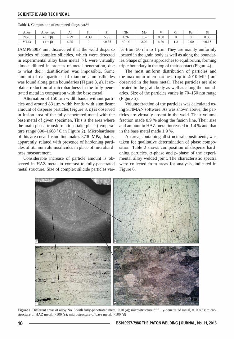
perimental alloy No.6 represents coarse elongated grains normal to fusion line (Figure 1). The structure and phase composition are determined by argon-arc welding thermal cycle (Figure 2).
Microhardness of the fully-penetrated metal made 3680 MPa, whereas, it reduced to 3430 MPa in HAZ metal, and then in the direction to base metal its val-ue increased to 4010 MPa. SEM examination on
© G.M. GRIGORENKO, S.V. AKHONIN, O.M. ZADOROZHNYUK and I.N. KLOCHKOV, 2016
10 ISSN 0957-798X THE PATON WELDING JOURNAL, No. 11, 2016
SCIENTIFIC AND TECHNICAL
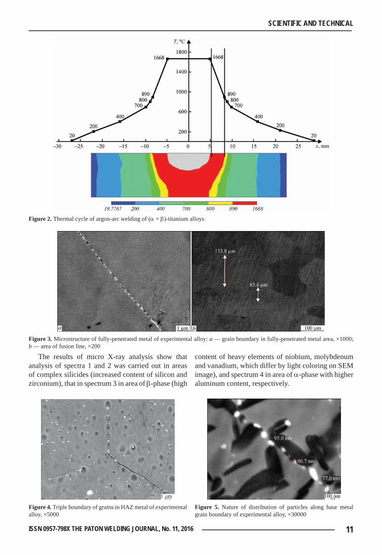
JAMP9500F unit discovered that the weld disperse particles of complex silicides, which were detected in experimental alloy base metal [7], were virtually almost diluted in process of metal penetration, due to what their identification was impossible. Some amount of nanoparticles of titanium alumosilicides was found along grain boundaries (Figure 3, a). It ex-plains reduction of microhardness in the fully-pene-trated metal in comparison with the base metal.
Alternation of 150 mm width bands without parti-cles and around 83 mm width bands with significant amount of disperse particles (Figure 3, b) is observed in fusion area of the fully-penetrated metal with the base metal of given specimen. This is the area where the main phase transformations take place (tempera-ture range 890–1668 °C in Figure 2). Microhardness of this area near fusion line makes 3730 MPa, that is, apparently, related with presence of hardening parti-cles of titanium alumosilicides in place of microhard-ness measurement.
Considerable increase of particle amount is ob-served in HAZ metal in contrast to fully-penetrated metal structure. Size of complex silicide particles var-
ies from 50 nm to 1 mm. They are mainly uniformly located in the grain body as well as along the boundar-ies. Shape of grains approaches to equilibrium, forming triple boundary in the top of their contact (Figure 4).
The most uniform distribution of particles and the maximum microhardness (up to 4010 MPa) are observed in the base metal. These particles are also located in the grain body as well as along the bound-aries. Size of the particles varies in 70–150 nm range (Figure 5).
Volume fraction of the particles was calculated us-ing STIMAN software. As was shown above, the par-ticles are virtually absent in the weld. Their volume fraction made 0.9 % along the fusion line. Their size and amount in HAZ metal increased to 1.4 % and that in the base metal made 1.9 %.
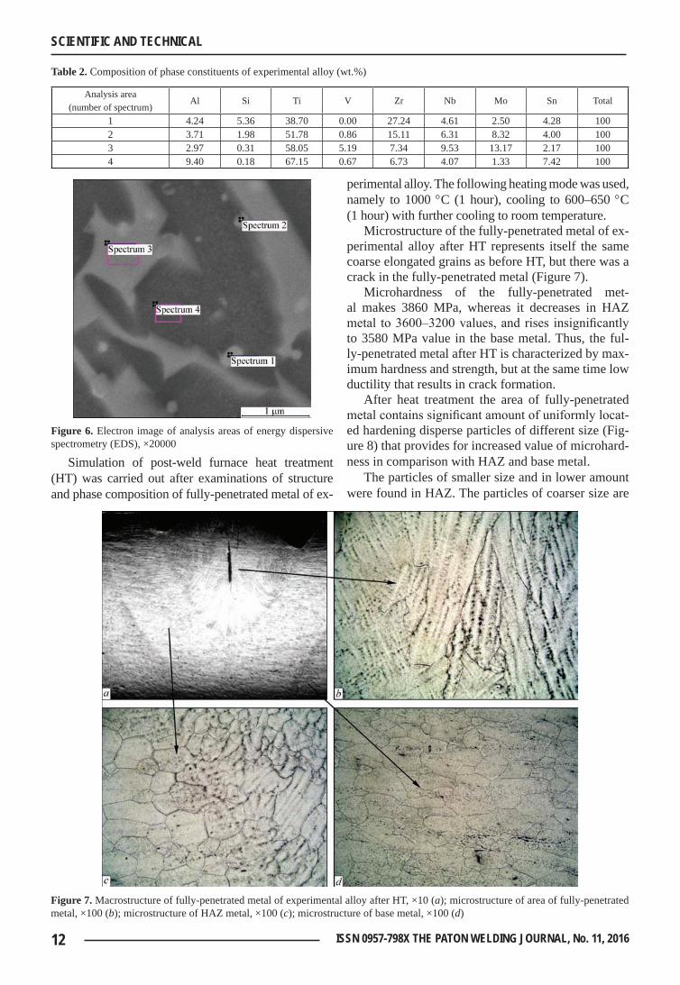
An area, containing all structural constituents, was taken for qualitative determination of phase compo-sition. Table 2 shows composition of disperse hard-ening particles, a-phase and b-phase of the experi-mental alloy welded joint. The characteristic spectra were collected from areas for analysis, indicated in Figure 6.
Table 1. Composition of examined alloys, wt.%
Alloy Alloy type Al Sn Zr Nb Mo V Cr Fe SiNo.6 (α + β) 4.29 4.39 5.95 4.26 1.57 0.68 0 0 0.35VT23 (α + β) 4.55 0 <0.35 <0.15 2.05 4.50 1.2 0.60 <0.15
Figure 1. Different areas of alloy No. 6 with fully-penetrated metal, ×10 (a); microstructure of fully-penetrated metal, ×100 (b); micro-structure of HAZ metal, ×100 (c); microstructure of base metal, ×100 (d)
11ISSN 0957-798X THE PATON WELDING JOURNAL, No. 11, 2016
SCIENTIFIC AND TECHNICAL
The results of micro X-ray analysis show that analysis of spectra 1 and 2 was carried out in areas of complex silicides (increased content of silicon and zirconium), that in spectrum 3 in area of b-phase (high
content of heavy elements of niobium, molybdenum and vanadium, which differ by light coloring on SEM image), and spectrum 4 in area of a-phase with higher aluminum content, respectively.
Figure 2. Thermal cycle of argon-arc welding of (a + b)-titanium alloys
Figure 3. Microstructure of fully-penetrated metal of experimental alloy: a — grain boundary in fully-penetrated metal area, ×1000; b — area of fusion line, ×200
Figure 4. Triple boundary of grains in HAZ metal of experimental alloy, ×5000
Figure 5. Nature of distribution of particles along base metal grain boundary of experimental alloy, ×30000
12 ISSN 0957-798X THE PATON WELDING JOURNAL, No. 11, 2016
SCIENTIFIC AND TECHNICAL
Simulation of post-weld furnace heat treatment (HT) was carried out after examinations of structure and phase composition of fully-penetrated metal of ex-
perimental alloy. The following heating mode was used, namely to 1000 °C (1 hour), cooling to 600–650 °C (1 hour) with further cooling to room temperature.
Microstructure of the fully-penetrated metal of ex-perimental alloy after HT represents itself the same coarse elongated grains as before HT, but there was a crack in the fully-penetrated metal (Figure 7).
Microhardness of the fully-penetrated met-al makes 3860 MPa, whereas it decreases in HAZ metal to 3600–3200 values, and rises insignificantly to 3580 MPa value in the base metal. Thus, the ful-ly-penetrated metal after HT is characterized by max-imum hardness and strength, but at the same time low ductility that results in crack formation.
After heat treatment the area of fully-penetrated metal contains significant amount of uniformly locat-ed hardening disperse particles of different size (Fig-ure 8) that provides for increased value of microhard-ness in comparison with HAZ and base metal.
The particles of smaller size and in lower amount were found in HAZ. The particles of coarser size are
Table 2. Composition of phase constituents of experimental alloy (wt.%)
Analysis area (number of spectrum)
Al Si Ti V Zr Nb Mo Sn Total
1 4.24 5.36 38.70 0.00 27.24 4.61 2.50 4.28 1002 3.71 1.98 51.78 0.86 15.11 6.31 8.32 4.00 1003 2.97 0.31 58.05 5.19 7.34 9.53 13.17 2.17 1004 9.40 0.18 67.15 0.67 6.73 4.07 1.33 7.42 100
Figure 6. Electron image of analysis areas of energy dispersive spectrometry (EDS), ×20000
Figure 7. Macrostructure of fully-penetrated metal of experimental alloy after HT, ×10 (a); microstructure of area of fully-penetrated metal, ×100 (b); microstructure of HAZ metal, ×100 (c); microstructure of base metal, ×100 (d)
13ISSN 0957-798X THE PATON WELDING JOURNAL, No. 11, 2016
SCIENTIFIC AND TECHNICAL
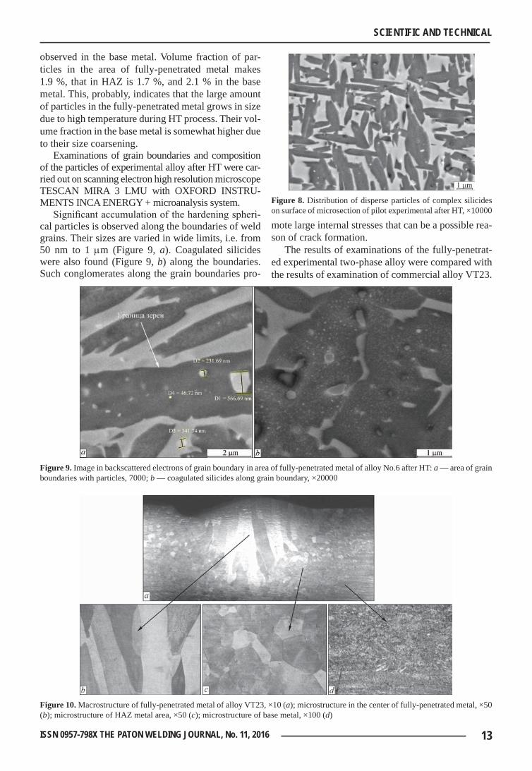
observed in the base metal. Volume fraction of par-ticles in the area of fully-penetrated metal makes 1.9 %, that in HAZ is 1.7 %, and 2.1 % in the base metal. This, probably, indicates that the large amount of particles in the fully-penetrated metal grows in size due to high temperature during HT process. Their vol-ume fraction in the base metal is somewhat higher due to their size coarsening.
Examinations of grain boundaries and composition of the particles of experimental alloy after HT were car-ried out on scanning electron high resolution microscope TESCAN MIRA 3 LMU with OXFORD INSTRU-MENTS INCA ENERGY + microanalysis system.
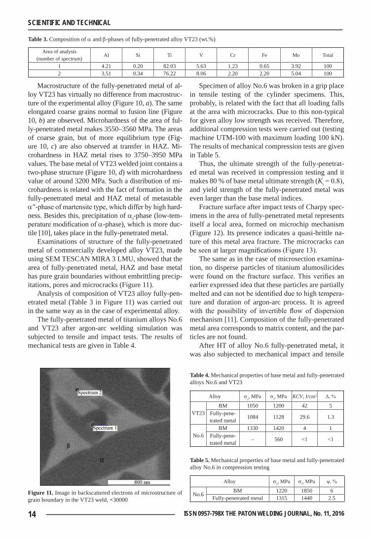
Significant accumulation of the hardening spheri-cal particles is observed along the boundaries of weld grains. Their sizes are varied in wide limits, i.e. from 50 nm to 1 mm (Figure 9, a). Coagulated silicides were also found (Figure 9, b) along the boundaries. Such conglomerates along the grain boundaries pro-
mote large internal stresses that can be a possible rea-son of crack formation.
The results of examinations of the fully-penetrat-ed experimental two-phase alloy were compared with the results of examination of commercial alloy VT23.
Figure 8. Distribution of disperse particles of complex silicides on surface of microsection of pilot experimental after HT, ×10000
Figure 9. Image in backscattered electrons of grain boundary in area of fully-penetrated metal of alloy No.6 after HT: a — area of grain boundaries with particles, 7000; b — coagulated silicides along grain boundary, ×20000
Figure 10. Macrostructure of fully-penetrated metal of alloy VT23, ×10 (a); microstructure in the center of fully-penetrated metal, ×50 (b); microstructure of HAZ metal area, ×50 (c); microstructure of base metal, ×100 (d)
14 ISSN 0957-798X THE PATON WELDING JOURNAL, No. 11, 2016
SCIENTIFIC AND TECHNICAL
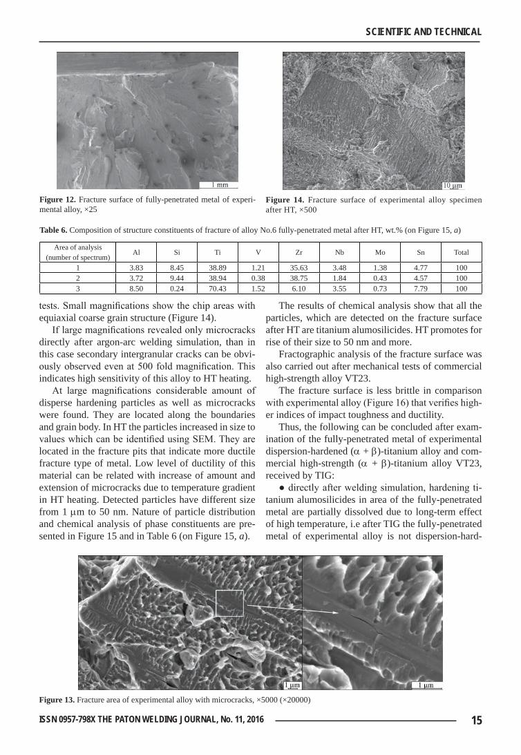
Macrostructure of the fully-penetrated metal of al-loy VT23 has virtually no difference from macrostruc-ture of the experimental alloy (Figure 10, a). The same elongated coarse grains normal to fusion line (Figure 10, b) are observed. Microhardness of the area of ful-ly-penetrated metal makes 3550–3560 MPa. The areas of coarse grain, but of more equilibrium type (Fig-ure 10, c) are also observed at transfer in HAZ. Mi-crohardness in HAZ metal rises to 3750–3950 MPa values. The base metal of VT23 welded joint contains a two-phase structure (Figure 10, d) with microhardness value of around 3200 MPa. Such a distribution of mi-crohardness is related with the fact of formation in the fully-penetrated metal and HAZ metal of metastable a′′-phase of martensite type, which differ by high hard-ness. Besides this, precipitation of al-phase (low-tem-perature modification of a-phase), which is more duc-tile [10], takes place in the fully-penetrated metal.
Examinations of structure of the fully-penetrated metal of commercially developed alloy VT23, made using SEM TESCAN MIRA 3 LMU, showed that the area of fully-penetrated metal, HAZ and base metal has pure grain boundaries without embrittling precip-itations, pores and microcracks (Figure 11).
Analysis of composition of VT23 alloy fully-pen-etrated metal (Table 3 in Figure 11) was carried out in the same way as in the case of experimental alloy.
The fully-penetrated metal of titanium alloys No.6 and VT23 after argon-arc welding simulation was subjected to tensile and impact tests. The results of mechanical tests are given in Table 4.
Specimen of alloy No.6 was broken in a grip place in tensile testing of the cylinder specimens. This, probably, is related with the fact that all loading falls at the area with microcracks. Due to this non-typical for given alloy low strength was received. Therefore, additional compression tests were carried out (testing machine UTM-100 with maximum loading 100 kN). The results of mechanical compression tests are given in Table 5.
Thus, the ultimate strength of the fully-penetrat-ed metal was received in compression testing and it makes 80 % of base metal ultimate strength (Kt = 0.8), and yield strength of the fully-penetrated metal was even larger than the base metal indices.
Fracture surface after impact tests of Charpy spec-imens in the area of fully-penetrated metal represents itself a local area, formed on microchip mechanism (Figure 12). Its presence indicates a quasi-brittle na-ture of this metal area fracture. The microcracks can be seen at larger magnifications (Figure 13).
The same as in the case of microsection examina-tion, no disperse particles of titanium alumosilicides were found on the fracture surface. This verifies an earlier expressed idea that these particles are partially melted and can not be identified due to high tempera-ture and duration of argon-arc process. It is agreed with the possibility of invertible flow of dispersion mechanism [11]. Composition of the fully-penetrated metal area corresponds to matrix content, and the par-ticles are not found.
After HT of alloy No.6 fully-penetrated metal, it was also subjected to mechanical impact and tensile
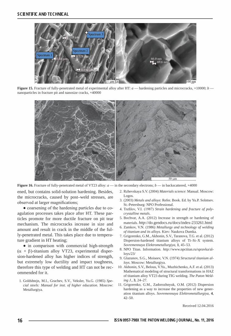
Table 3. Composition of a and b-phases of fully-penetrated alloy VT23 (wt.%)
Area of analysis (number of spectrum)
Al Si Ti V Cr Fe Mo Total
1 4.21 0.20 82.03 5.63 1.23 0.65 3.92 1002 3.51 0.34 76.22 8.06 2.20 2.20 5.04 100
Figure 11. Image in backscattered electrons of microstructure of grain boundary in the VT23 weld, ×30000
Table 4. Mechanical properties of base metal and fully-penetrated alloys No.6 and VT23
Alloy sy, MPa st, MPa KCV, J/cm2 Δ, %
VT23BM 1050 1200 42 5
Fully-pene-trated metal 1084 1128 29.6 1.3
No.6BM 1330 1420 4 1
Fully-pene-trated metal – 560 <1 <1
Table 5. Mechanical properties of base metal and fully-penetrated alloy No.6 in compression testing
Alloy sy, MPa st, MPa ψ, %
No.6BM 1220 1850 6
Fully-penetrated metal 1315 1440 2.5
15ISSN 0957-798X THE PATON WELDING JOURNAL, No. 11, 2016
SCIENTIFIC AND TECHNICAL
tests. Small magnifications show the chip areas with equiaxial coarse grain structure (Figure 14).
If large magnifications revealed only microcracks directly after argon-arc welding simulation, than in this case secondary intergranular cracks can be obvi-ously observed even at 500 fold magnification. This indicates high sensitivity of this alloy to HT heating.
At large magnifications considerable amount of disperse hardening particles as well as microcracks were found. They are located along the boundaries and grain body. In HT the particles increased in size to values which can be identified using SEM. They are located in the fracture pits that indicate more ductile fracture type of metal. Low level of ductility of this material can be related with increase of amount and extension of microcracks due to temperature gradient in HT heating. Detected particles have different size from 1 mm to 50 nm. Nature of particle distribution and chemical analysis of phase constituents are pre-sented in Figure 15 and in Table 6 (on Figure 15, a).
The results of chemical analysis show that all the particles, which are detected on the fracture surface after HT are titanium alumosilicides. HT promotes for rise of their size to 50 nm and more.
Fractographic analysis of the fracture surface was also carried out after mechanical tests of commercial high-strength alloy VT23.
The fracture surface is less brittle in comparison with experimental alloy (Figure 16) that verifies high-er indices of impact toughness and ductility.
Thus, the following can be concluded after exam-ination of the fully-penetrated metal of experimental dispersion-hardened (a + b)-titanium alloy and com-mercial high-strength (a + b)-titanium alloy VT23, received by TIG:
● directly after welding simulation, hardening ti-tanium alumosilicides in area of the fully-penetrated metal are partially dissolved due to long-term effect of high temperature, i.e after TIG the fully-penetrated metal of experimental alloy is not dispersion-hard-
Figure 12. Fracture surface of fully-penetrated metal of experi-mental alloy, ×25
Figure 13. Fracture area of experimental alloy with microcracks, ×5000 (×20000)
Figure 14. Fracture surface of experimental alloy specimen after HT, ×500
Table 6. Composition of structure constituents of fracture of alloy No.6 fully-penetrated metal after HT, wt.% (on Figure 15, a)
Area of analysis (number of spectrum)
Al Si Ti V Zr Nb Mo Sn Total
1 3.83 8.45 38.89 1.21 35.63 3.48 1.38 4.77 1002 3.72 9.44 38.94 0.38 38.75 1.84 0.43 4.57 1003 8.50 0.24 70.43 1.52 6.10 3.55 0.73 7.79 100
16 ISSN 0957-798X THE PATON WELDING JOURNAL, No. 11, 2016
SCIENTIFIC AND TECHNICAL
ened, but contains solid-solution hardening. Besides, the microcracks, caused by post–weld stresses, are observed at larger magnifications;
● coarsening of the hardening particles due to co-agulation processes takes place after HT. These par-ticles promote for more ductile fracture on pit tear mechanism. The microcracks increase in size and amount and result in crack in the middle of the ful-ly-penetrated metal. This takes place due to tempera-ture gradient in HT heating;
● in comparison with commercial high-strength (a + b)-titanium alloy VT23, experimental disper-sion-hardened alloy has higher indices of strength, but extremely low ductility and impact toughness, therefore this type of welding and HT can not be rec-ommended for it.
1. Goldshtejn, M.I., Grachev, S.V., Veksler, Yu.G. (1985) Spe-cial steels: Manual for inst. of higher education. Moscow: Metallurgiya.
2. Rzhevskaya S.V. (2004) Materials science: Manual. Moscow: Logos.
3. (2003) Metals and alloys: Refer. Book. Ed. by Yu.P. Solntsev. St.-Petersburg: NPO Professional.
4. Trefilov, V.I. (1987) Strain hardening and fracture of poly-crystalline metals.
5. Bochvar, A.A. (2012) Increase in strength or hardening of materials. http://do.gendocs.ru/docs/index-233261.html
6. Zamkov, V.N. (1986) Metallurgy and technology of welding of titanium and its alloys. Kiev: Naukova Dumka.
7. Grigorenko, G.M., Akhonin, S.V., Taranova, T.G. et al. (2012) Dispersion-hardened titanium alloys of Ti–Si–X system. Sovremennaya Elektrometallurgiya, 1, 45–53.
8. NPO Titan. Information. http://www.npctitan.ru/spravka/al-loys/23/
9. Glazunov, S.G., Moiseev, V.N. (1974) Structural titanium al-loys. Moscow: Metallurgiya.
10. Akhonin, S.V., Belous, V.Yu., Muzhichenko, A.F. et al. (2013) Mathematical modeling of structural transformations in HAZ of titanium alloy VT23 during TIG welding. The Paton Weld-ing J., 3, 24–27.
11. Grigorenko, G.M., Zadorozhnyuk, O.M. (2012) Dispersion hardening as a way to increase the properties of new gener-ation titanium alloys. Sovremennaya Elektrometallurgiya, 4, 42–50.
Received 12.04.2016
Figure 15. Fracture of fully-penetrated metal of experimental alloy after HT: a — hardening particles and microcracks, ×10000; b — nanoparticles in fracture pit and nanosize cracks, ×40000
Figure 16. Fracture of fully-penetrated metal of VT23 alloy: a — in the secondary electrons; b — in backscattered, ×4000
17ISSN 0957-798X THE PATON WELDING JOURNAL, No. 11, 2016
INDUSTRIAL
doi.org/10.15407/tpwj2016.11.03
INFLUENCE OF METHODS OF ARC SURFACING WITH FLUX-CORED WIRE ON PENETRATION
OF BASE METAL AND FORMATION OF DEPOSITED METALA.A. BABINETS1, I.A. RYABTSEV1, A.I. PANFILOV2, V.A. ZHDANOV1 and I.I. RYABTSEV1
1E.O. Paton Electric Welding Institute, NASU 11 Kazimir Malevich Str., 03680, Kiev, Ukraine. E-mail: [email protected]
2OJSC «Steel Work» 13 Tbilisskaya Str. 50005, Krivoy Rog, Ukraine
The influence of methods of automatic arc surfacing on penetration of base metal, quality of formation and geometric sizes of deposited beads was investigated. In the experiments nine batches of flux-cored wires (25Kh5FMS type of deposited metal) of the diameter of 1.8; 2.4 and 2.8 mm for submerged arc, shielding gas and open arc surfacing were used. The surfacing was carried out in a wide range of modes: Is = 150–450 A; Us = 20–34 V at the same surfacing speed of 20 m/h. It was found that the greatest influence on formation of deposited beads is exerted by arc voltage. Moreover, the range of DUT voltages, at which a good formation of deposited beads and absence of pores is provided, does not coincide during surfacing by different methods with wire of the same diameter. The results obtained in this work can be used for selecting the method of arc surfacing, surfacing modes, which ultimately meet the operating conditions and the requirements to the deposited metal for definite parts. These results will be also used in databases in the development of computer programs for robotized additive technologies of arc surfacing. 13 Ref., 1 Table, 6 Figures.
K e y w o r d s : arc surfacing, surfacing modes, additive technologies of surfacing, flux-cored wire, deposited metal, penetration, formation of deposited metal
Flux-cored wire is one of the most universal electrode materials for mechanized and automated arc surfacing (welding) [1–3]. Among the main advantages of flux-cored wire, as compared to the other electrode mate-rials, a rather simple adaptation of its chemical com-position to the composition and properties of the parts being deposited, high arc burning stability, relatively low spattering of electrode metal and good formation of deposited beads can be mentioned [4–8].
Depending on the method of surfacing the flux-cored wires can be divided into three classes: for sub-merged arc surfacing, surfacing in the shielding gases and using open arc (self-shielding) [1, 9].
It is widely known, that the surfacing modes have a significant effect on penetration of base metal and quality of formation of deposited metal [1–10]. However, in most cases, the data presented in the mentioned works are uncoordinated, because they describe the properties of deposited metal produced using different methods applying different surfacing materials and modes. Moreover, when developing the technology for surfacing of different parts it is often necessary to provide not only the quality and preset properties of deposited metal, but also the specified geometric sizes of deposited beads and volume of base metal in the deposited metal (VBMD), etc. [9].
The aim of this work is the systematic investiga-tion of influence of different methods of automatic arc surfacing and surfacing parameters on penetration of base metal, quality of formation and geometric sizes of deposited beads using surfacing materials of the same chemical composition and diameters.
The accumulation of databases on the modes of different methods of arc surfacing, geometric sizes of deposited beads, VBMD values and the value of penetration considering the previously developed ex-pert systems on surfacing technologies [11, 12] and the proposed computer system advisor for selection of technology for surfacing typical parts [13] can further serve as a basis for development of computer programs for robotized additive technologies of arc surfacing.
Materials and methods of investigations. For in-vestigations nine batches of experimental flux-cored wires were manufactured for submerged arc surfacing (AN-26P), shielding gas (82 % Ar + 18 % CO2) and with open arc applying self-shielding flux-cored wire (shielding system CaO + TiO2 + MgO + CaF2 + Al2O3) of the diameters of 1.8; 2.4 and 2.8 mm. The metallic part of the charge of flux-cored wires was calculated in the way to produce deposited metal of one type: 25Kh5FMS. For surfacing the universal surfacing in-stallation U-653 was used, completed with the pow-
© A.A. BABINETS, I.A. RYABTSEV, A.I. PANFILOV, V.A. ZHDANOV and I.I. RYABTSEV, 2016
18 ISSN 0957-798X THE PATON WELDING JOURNAL, No. 11, 2016
INDUSTRIAL
er source VDU-506. The surfacing using flux-cored wires of different types and diameters was carried out on the plates of St.3 steel of 15 mm thickness in a wide range of modes: surfacing current Is was from 150 to 450 A; voltage Us was from 20 to 34 V. The record and control of electrical parameters of surfacing mode was performed using the developed computer infor-mation-measuring system [13]. The surfacing speed of 20 m/h in all the experiments remained constant, because in the range of 20–40 m/h at other unchanged parameters the surfacing speed almost does not affect the geometric sizes of deposited beads [9].
In the process of the experiments the expert eval-uation of quality of deposited bead formation, pres-ence of pores, etc. was carried out. For measurements of basic geometric parameters of deposited beads on macrosections, cut out from deposited workpieces, the instrumental microscope BMI-1 was used. The mean value of go (VBMD) was determined according to six-eight cross-sections for each deposited bead ac-cording to the formula
100 %,b
bb d
FF Fg = ⋅
+
where Fb, Fd are cross-sectional areas of molten base metal and deposited metals, respectively.
The obtained data were entered to the table gen-eral for each method. As an example, below the table is presented with characteristics of separate beads, deposited by submerged arc surfacing, surfacing in shielding gases and using open arc with flux-cored wires of 1.8 mm diameter.
Influence of methods and modes of surfacing on geometric sizes of deposited beads and VBMD. The basic parameters of surfacing mode are: current value, polarity and type; arc voltage; surfacing speed; elec-trode diameter and surfacing pitch [9]. In surfacing of rotation bodies the basic parameters include also the displacement from zenith (deposition of outer surfac-es) or nadir (deposition of inner surfaces).
One of the most important characteristics of sur-facing process are penetration value and volume of base metal. It is widely known that with decrease in
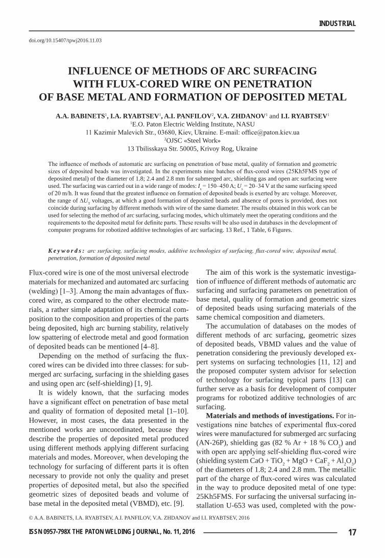
Influence of surfacing mode using flux-cored wires of 1.8 mm diameter on formation of deposited metal and VBMD depending on the method of surfacing
NumberSurfacing mode
Formation (presence of pores) VBMD, % Appearance of deposited beadsIs, А Us, V
Submerged arc surfacing1 241 26.9 Satisfactory. Narrow bead 30.52 245 27.9 Good 443 290 27.8 Poor 44.54 298 27.7 Poor 51.35 301 28.9 Good 446 311 28.6 Satisfactory 48.5
7 224 26.5 Poor. Narrow bead 25.5
Shielding gas surfacing1 237 26.5 Good 42.52 331 26.5 Good 503 316 27.3 Good 464 272 27.6 Satisfactory (pores) 505 171 28.3 Satisfactory (pores) 49.36 161 26.7 Satisfactory 50
7 172 23.0 Satisfactory. Narrow bead 25.8
Open arc surfacing1 256 23.4 Good 47.52 239 23.7 Good 45.53 227 22.3 Good. Narrow bead 484 236 22.2 Good. Narrow bead 38.55 218 22.3 Good. Narrow bead 51.5
6 232 23.3 Satisfactory. Narrow bead 26.5
19ISSN 0957-798X THE PATON WELDING JOURNAL, No. 11, 2016
INDUSTRIAL
penetration and VBMD not only the consumption of expensive surfacing materials is reduced, but also the quality and operating properties of deposited parts are improved. According to (1), VBMD value depends on the cross-section area of molten base and depos-ited metal. Thus, VBMD will decrease if the growth of surfacing area occurs faster than the growth of the area of molten base metal.
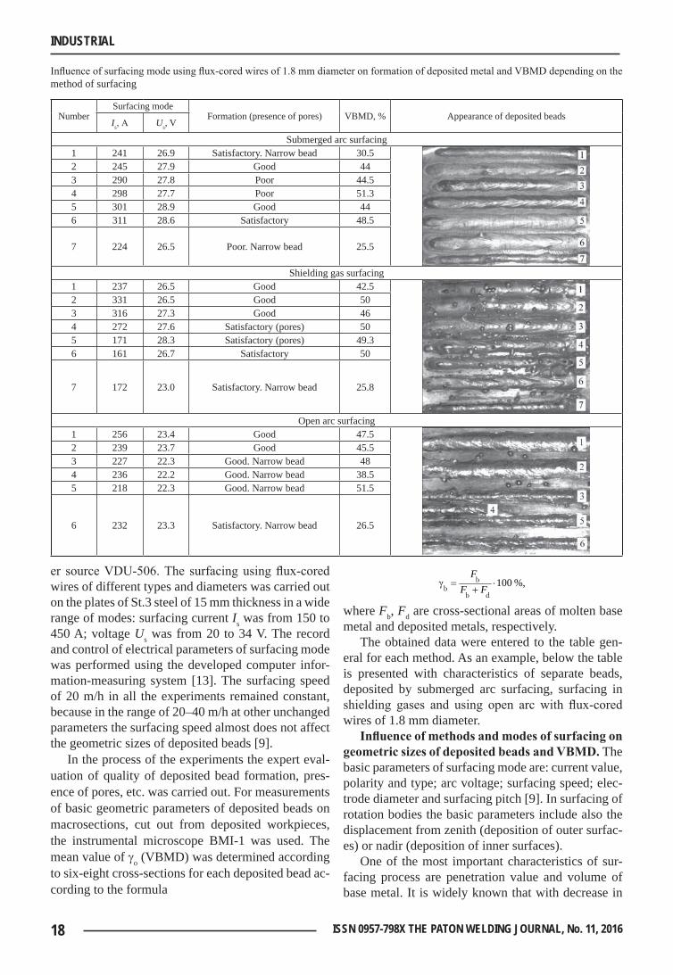
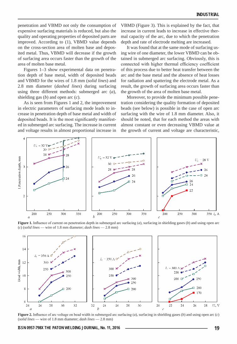
Figures 1–3 show experimental data on penetra-tion depth of base metal, width of deposited beads and VBMD for the wires of 1.8 mm (solid lines) and 2.8 mm diameter (dashed lines) during surfacing using three different methods: submerged arc (a), shielding gas (b) and open arc (c).
As is seen from Figures 1 and 2, the improvement in electric parameters of surfacing mode leads to in-crease in penetration depth of base metal and width of deposited beads. It is the most significantly manifest-ed in submerged arc surfacing. The increase in current and voltage results in almost proportional increase in
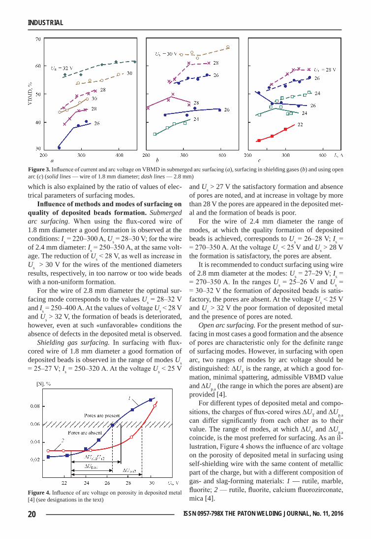
VBMD (Figure 3). This is explained by the fact, that increase in current leads to increase in effective ther-mal capacity of the arc, due to which the penetration depth and rate of electrode melting are increased.
It was found that at the same mode of surfacing us-ing wire of one diameter, the lower VBMD can be ob-tained in submerged arc surfacing. Obviously, this is connected with higher thermal efficiency coefficient of this process due to better heat transfer between the arc and the base metal and the absence of heat losses for radiation and spattering the electrode metal. As a result, the growth of surfacing area occurs faster than the growth of the area of molten base metal.
Moreover, to provide the minimum possible pene-tration considering the quality formation of deposited beads (see below) is possible in the case of open arc surfacing with the wire of 1.8 mm diameter. Also, it should be noted, that for each method the areas with almost constant or even decreasing VBMD value at the growth of current and voltage are characteristic,
Figure 1. Influence of current on penetration depth in submerged arc surfacing (a), surfacing in shielding gases (b) and using open arc (c) (solid lines — wire of 1.8 mm diameter; dash lines — 2.8 mm)
Figure 2. Influence of arc voltage on bead width in submerged arc surfacing (a), surfacing in shielding gases (b) and using open arc (c) (solid lines — wire of 1.8 mm diameter; dash lines — 2.8 mm)
20 ISSN 0957-798X THE PATON WELDING JOURNAL, No. 11, 2016
INDUSTRIAL
which is also explained by the ratio of values of elec-trical parameters of surfacing modes.
Influence of methods and modes of surfacing on quality of deposited beads formation. Submerged arc surfacing. When using the flux-cored wire of 1.8 mm diameter a good formation is observed at the conditions: Is = 220–300 A, Us = 28–30 V; for the wire of 2.4 mm diameter: Is = 250–350 A, at the same volt-age. The reduction of Us < 28 V, as well as increase in Us > 30 V for the wires of the mentioned diameters results, respectively, in too narrow or too wide beads with a non-uniform formation.
For the wire of 2.8 mm diameter the optimal sur-facing mode corresponds to the values Us = 28–32 V and Is = 250–400 A. At the values of voltage Us < 28 V and Us > 32 V, the formation of beads is deteriorated, however, even at such «unfavorable» conditions the absence of defects in the deposited metal is observed.
Shielding gas surfacing. In surfacing with flux-cored wire of 1.8 mm diameter a good formation of deposited beads is observed in the range of modes Us = 25–27 V; Is = 250–320 A. At the voltage Us < 25 V
and Us > 27 V the satisfactory formation and absence of pores are noted, and at increase in voltage by more than 28 V the pores are appeared in the deposited met-al and the formation of beads is poor.
For the wire of 2.4 mm diameter the range of modes, at which the quality formation of deposited beads is achieved, corresponds to Us = 26–28 V; Is = = 270–350 A. At the voltage Us < 25 V and Us > 28 V the formation is satisfactory, the pores are absent.
It is recommended to conduct surfacing using wire of 2.8 mm diameter at the modes: Us = 27–29 V; Is = = 270–350 A. In the ranges Us = 25–26 V and Us = = 30–32 V the formation of deposited beads is satis-factory, the pores are absent. At the voltage Us < 25 V and Us > 32 V the poor formation of deposited metal and the presence of pores are noted.
Open arc surfacing. For the present method of sur-facing in most cases a good formation and the absence of pores are characteristic only for the definite range of surfacing modes. However, in surfacing with open arc, two ranges of modes by arc voltage should be distinguished: DUT is the range, at which a good for-mation, minimal spattering, admissible VBMD value and DUp.a (the range in which the pores are absent) are provided [4].
For different types of deposited metal and compo-sitions, the charges of flux-cored wires DUT and DUp.a can differ significantly from each other as to their value. The range of modes, at which DUT and DUp.a coincide, is the most preferred for surfacing. As an il-lustration, Figure 4 shows the influence of arc voltage on the porosity of deposited metal in surfacing using self-shielding wire with the same content of metallic part of the charge, but with a different composition of gas- and slag-forming materials: 1 — rutile, marble, fluorite; 2 — rutile, fluorite, calcium fluorozirconate, mica [4].
Figure 3. Influence of current and arc voltage on VBMD in submerged arc surfacing (a), surfacing in shielding gases (b) and using open arc (c) (solid lines — wire of 1.8 mm diameter; dash lines — 2.8 mm)
Figure 4. Influence of arc voltage on porosity in deposited metal [4] (see designations in the text)
21ISSN 0957-798X THE PATON WELDING JOURNAL, No. 11, 2016
INDUSTRIAL
The carried out investigations showed that for self-shielding wire of 1.8 mm diameter a good forma-tion of deposited beads and absence of pores are char-acteristic for the modes Us = 22–24 V at the current Is = 200–250 A. At the voltage Us < 22 V the shape of beads is narrow, the formation is satisfactory. At Us > 24 V almost in the whole range of currents a significant number of pores and a poor formation of beads are observed. Also at the increase in current and voltage the spattering of metal is increased.
In surfacing with self-shielding flux-cored wires of 2.4 and 2.8 mm diameter the stable process with a good formation of deposited beads and absence of pores in them is characteristic for surfacing modes Us = 23–25 V; Is = 220–300 A. For beads, deposited at the modes Us < 23 V and Us = 25–27 V, the absence of pores is also characteristic, but their shape and surface quality can be regarded as not good enough. At the voltage of Us > 27 V the process becomes unstable, the beads are characterized by poor formation and the presence of numerous pores.
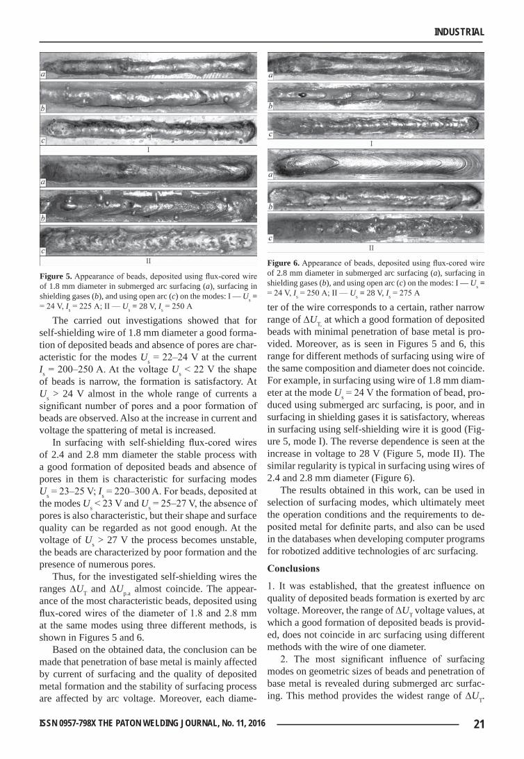
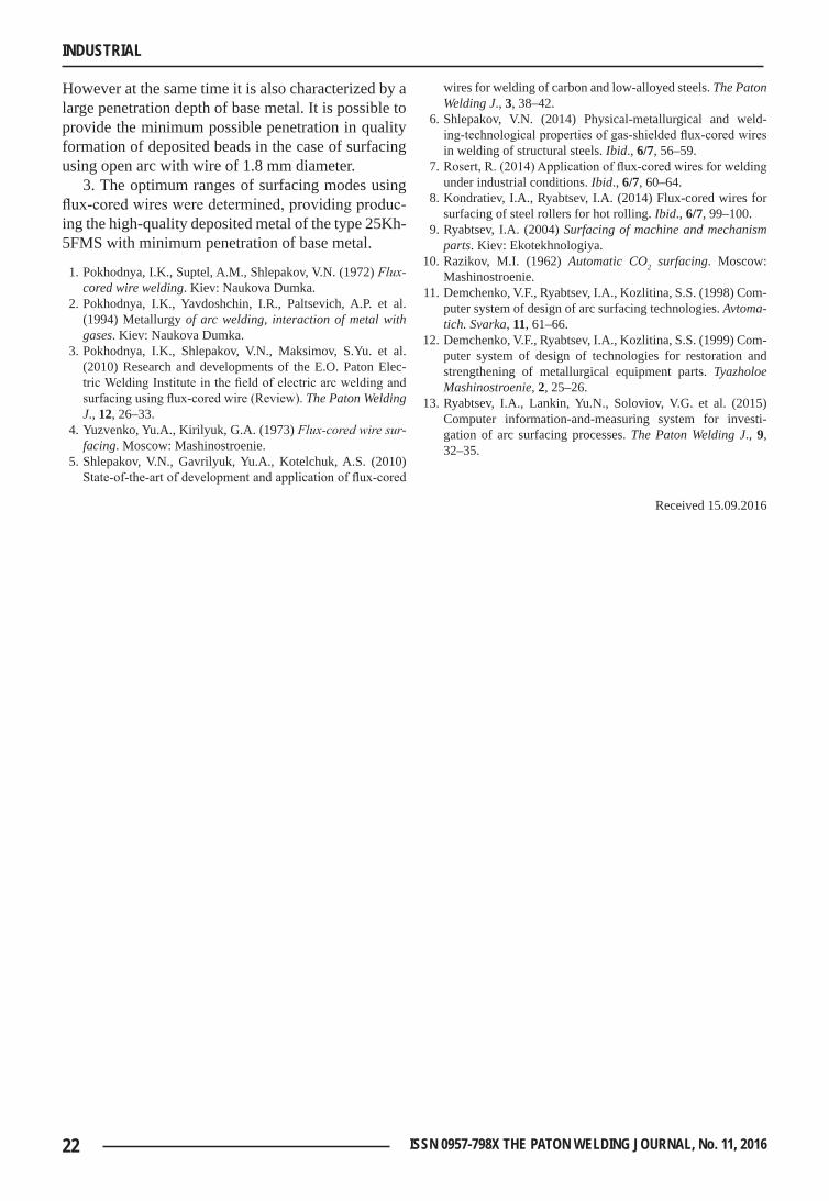
Thus, for the investigated self-shielding wires the ranges DUT and DUp.a almost coincide. The appear-ance of the most characteristic beads, deposited using flux-cored wires of the diameter of 1.8 and 2.8 mm at the same modes using three different methods, is shown in Figures 5 and 6.
Based on the obtained data, the conclusion can be made that penetration of base metal is mainly affected by current of surfacing and the quality of deposited metal formation and the stability of surfacing process are affected by arc voltage. Moreover, each diame-
ter of the wire corresponds to a certain, rather narrow range of DUT, at which a good formation of deposited beads with minimal penetration of base metal is pro-vided. Moreover, as is seen in Figures 5 and 6, this range for different methods of surfacing using wire of the same composition and diameter does not coincide. For example, in surfacing using wire of 1.8 mm diam-eter at the mode Us = 24 V the formation of bead, pro-duced using submerged arc surfacing, is poor, and in surfacing in shielding gases it is satisfactory, whereas in surfacing using self-shielding wire it is good (Fig-ure 5, mode I). The reverse dependence is seen at the increase in voltage to 28 V (Figure 5, mode II). The similar regularity is typical in surfacing using wires of 2.4 and 2.8 mm diameter (Figure 6).
The results obtained in this work, can be used in selection of surfacing modes, which ultimately meet the operation conditions and the requirements to de-posited metal for definite parts, and also can be used in the databases when developing computer programs for robotized additive technologies of arc surfacing.
Conclusions
1. It was established, that the greatest influence on quality of deposited beads formation is exerted by arc voltage. Moreover, the range of DUT voltage values, at which a good formation of deposited beads is provid-ed, does not coincide in arc surfacing using different methods with the wire of one diameter.
2. The most significant influence of surfacing modes on geometric sizes of beads and penetration of base metal is revealed during submerged arc surfac-ing. This method provides the widest range of DUT.
Figure 5. Appearance of beads, deposited using flux-cored wire of 1.8 mm diameter in submerged arc surfacing (a), surfacing in shielding gases (b), and using open arc (c) on the modes: I — Us = = 24 V, Is = 225 А; II — Us = 28 V, Is = 250 А
Figure 6. Appearance of beads, deposited using flux-cored wire of 2.8 mm diameter in submerged arc surfacing (a), surfacing in shielding gases (b), and using open arc (c) on the modes: I — Us = = 24 V, Is = 250 А; II — Us = 28 V, Is = 275 А
22 ISSN 0957-798X THE PATON WELDING JOURNAL, No. 11, 2016
INDUSTRIAL
However at the same time it is also characterized by a large penetration depth of base metal. It is possible to provide the minimum possible penetration in quality formation of deposited beads in the case of surfacing using open arc with wire of 1.8 mm diameter.
3. The optimum ranges of surfacing modes using flux-cored wires were determined, providing produc-ing the high-quality deposited metal of the type 25Kh-5FMS with minimum penetration of base metal.
1. Pokhodnya, I.K., Suptel, A.M., Shlepakov, V.N. (1972) Flux-cored wire welding. Kiev: Naukova Dumka.
2. Pokhodnya, I.K., Yavdoshchin, I.R., Paltsevich, A.P. et al. (1994) Metallurgy of arc welding, interaction of metal with gases. Kiev: Naukova Dumka.
3. Pokhodnya, I.K., Shlepakov, V.N., Maksimov, S.Yu. et al. (2010) Research and developments of the E.O. Paton Elec-tric Welding Institute in the field of electric arc welding and surfacing using flux-cored wire (Review). The Paton Welding J., 12, 26–33.
4. Yuzvenko, Yu.A., Kirilyuk, G.A. (1973) Flux-cored wire sur-facing. Moscow: Mashinostroenie.
5. Shlepakov, V.N., Gavrilyuk, Yu.A., Kotelchuk, A.S. (2010) State-of-the-art of development and application of flux-cored
wires for welding of carbon and low-alloyed steels. The Paton Welding J., 3, 38–42.
6. Shlepakov, V.N. (2014) Physical-metallurgical and weld-ing-technological properties of gas-shielded flux-cored wires in welding of structural steels. Ibid., 6/7, 56–59.
7. Rosert, R. (2014) Application of flux-cored wires for welding under industrial conditions. Ibid., 6/7, 60–64.
8. Kondratiev, I.A., Ryabtsev, I.A. (2014) Flux-cored wires for surfacing of steel rollers for hot rolling. Ibid., 6/7, 99–100.
9. Ryabtsev, I.A. (2004) Surfacing of machine and mechanism parts. Kiev: Ekotekhnologiya.
10. Razikov, M.I. (1962) Automatic CO2 surfacing. Moscow: Mashinostroenie.
11. Demchenko, V.F., Ryabtsev, I.A., Kozlitina, S.S. (1998) Com-puter system of design of arc surfacing technologies. Avtoma-tich. Svarka, 11, 61–66.
12. Demchenko, V.F., Ryabtsev, I.A., Kozlitina, S.S. (1999) Com-puter system of design of technologies for restoration and strengthening of metallurgical equipment parts. Tyazholoe Mashinostroenie, 2, 25–26.
13. Ryabtsev, I.A., Lankin, Yu.N., Soloviov, V.G. et al. (2015) Computer information-and-measuring system for investi-gation of arc surfacing processes. The Paton Welding J., 9, 32–35.
Received 15.09.2016

23ISSN 0957-798X THE PATON WELDING JOURNAL, No. 11, 2016
SCIENTIFIC AND TECHNICAL
doi.org/10.15407/tpwj2016.11.04
PECULIARITIES OF BEAD SHAPE REGULATION IN SINGLE-LAYER MICROPLASMA SURFACING ON EDGES
OF AIRCRAFT GAS TURBINE ENGINE BLADES*
P.D. ZHEMANYUK1, I.A. PETRIK1, S.L. CHIGILEJCHIK1, A.V. YAROVITSYN2 and G.D. KHRUSHCHOV2
1JSC «Motor Sich» 15 Motorostroiteley Str., 69068, Zaporozhe, Ukraine. E-mail:[email protected]
2 E.O. Paton Electric Welding Institute, NASU 11 Kazimir Malevich Str., 03680, Kiev, Ukraine. E-mail: [email protected]
It is a necessary to specify the dependencies of deposited metal shaping due to the need of 5–15 mm height increase of the dimensions of surfacing-repaired damaged areas of blade edges of aircraft GTE of high-temperature nickel alloys in microplasma bead surfacing on narrow substrate of less than 3 mm. A range of change of the process energy indices in «effective heat power of arc–heat input–cross-section area of deposited bead» system was investigated for conditions of corresponding single-layer surfacing, and effectiveness of process regulation of deposited layer cross-section was eval-uated. It is determined that heat input change in 100–1600 J/mm range is the most effective regulation of cross-section area of the deposited bead under conditions of base metal limited penetration depth. It is assumed that the determined process relationship between heat input energy, height and cross-section area of the deposited bead will promote for formation of the additional criteria preventing crack formation in the «base–deposited metal» welded joint in repair of the parts of aircraft engines of high-temperature nickel alloys using multi-layer microplasma powder surfacing. 18 Ref., 4 Tables, 8 Figures.
K e y w o r d s : microplasma powder surfacing, high-temperature nickel alloy and heat-resistant cobalt alloy, narrow substrate, effective heat power of arc, heat input, thermal efficiency, cross-section area of deposited bead
One of the fields of application of arc surfacing on narrow substrate [1] of up to 3 mm width is the series repair of damaged or worn edges of aircraft gas tur-bine engine (GTE) blades [2–8]. The working blades of serially repaired aircraft engines D18T, D436, AI222, AI-450 are manufactured of nickel high-tem-perature alloys with polycrystalline structure (Zh-S6U-VI, ZhS6K-VI) or of directionally-solidified al-loys (ZhS32-VI and ZhS26-VI) [9]. These high-alloy materials, containing 55 and more vol.% of g′-phase, are designed for operation at 1000–1100 °C tempera-tures and differ by high tendency to crack formation in fusion welding and/or further heat treatment [9, 10]. Argon-arc welding has been used for repair of such parts for more than 40 years, however, repair of the blade edges was limited by up to 2 mm depth and filler metal was inferior to base metal on heat resis-tance [2, 3].
Microplasma powder surfacing [4–8] has been successfully used for more than 10 years at JSC «Mo-tor Sich» and SE «Ivchenko-Progress» for repair of aircraft working blades of given alloys with more than 3–5 thou. h. running. Several grades of filler powders,
in particular, high-temperature nickel alloy ZhS32 [4–8] and high-temperature cobalt and wear-resistant alloy V3K [5, 8], are widely used in this process.
Currently, serial repair production requires in-crease of dimensions of surfacing-repaired areas of blades (edges of platforms, labyrinth ends, Z-shape profiles and blade airfoil) to 5–15 mm height due to corresponding increase of size of wear zones, burn-through and thermal fatigue cracks, developing in process of operation of these parts. Their restoration can be characterized as process of multi-layer surfac-ing, in which «base–deposited metal» welded joint can under certain conditions be susceptible to forma-tion of micro- and macrocracks [6, 10, 11]. In turn, the multi-layer surfacing at some approximation can be presented as collection of single-layer beads. There-fore, it is relevant to expand the knowledges on the boundaries of energy indices range in single-layer surfacing for reasonable selection of such level and methods of balancing of heat input in the part, which provide for process strength of given welded joint, i.e. susceptibility of mentioned above materials to crack formation in fusion welding is not developed.
*Based on materials of paper, presented at the International Conference «Current welding technologies», July 11–13, 2016, Kiev, E.O. Paton Electric Welding Institute of the NAS of Ukraine.
© P.D. ZHEMANYUK, I.A. PETRIK, S.L. CHIGILEJCHIK, A.V. YAROVITSYN and G.D. KHRUSHCHOV, 2016
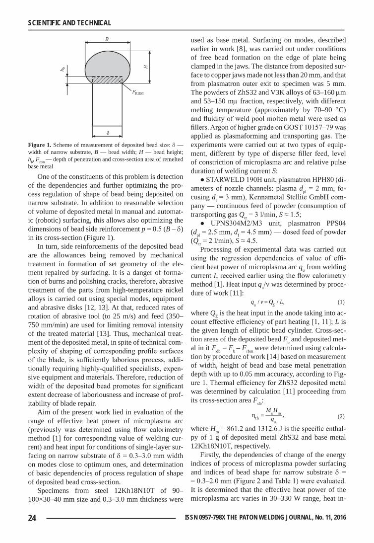
24 ISSN 0957-798X THE PATON WELDING JOURNAL, No. 11, 2016
SCIENTIFIC AND TECHNICAL
One of the constituents of this problem is detection of the dependencies and further optimizing the pro-cess regulation of shape of bead being deposited on narrow substrate. In addition to reasonable selection of volume of deposited metal in manual and automat-ic (robotic) surfacing, this allows also optimizing the dimensions of bead side reinforcement p = 0.5 (B – d) in its cross-section (Figure 1).
In turn, side reinforcements of the deposited bead are the allowances being removed by mechanical treatment in formation of set geometry of the ele-ment repaired by surfacing. It is a danger of forma-tion of burns and polishing cracks, therefore, abrasive treatment of the parts from high-temperature nickel alloys is carried out using special modes, equipment and abrasive disks [12, 13]. At that, reduced rates of rotation of abrasive tool (to 25 m/s) and feed (350–750 mm/min) are used for limiting removal intensity of the treated material [13]. Thus, mechanical treat-ment of the deposited metal, in spite of technical com-plexity of shaping of corresponding profile surfaces of the blade, is sufficiently laborious process, addi-tionally requiring highly-qualified specialists, expen-sive equipment and materials. Therefore, reduction of width of the deposited bead promotes for significant extent decrease of laboriousness and increase of prof-itability of blade repair.
Aim of the present work lied in evaluation of the range of effective heat power of microplasma arc (previously was determined using flow calorimetry method [1] for corresponding value of welding cur-rent) and heat input for conditions of single-layer sur-facing on narrow substrate of d = 0.3–3.0 mm width on modes close to optimum ones, and determination of basic dependencies of process regulation of shape of deposited bead cross-section.
Specimens from steel 12Kh18N10T of 90–100×30–40 mm size and 0.3–3.0 mm thickness were
used as base metal. Surfacing on modes, described earlier in work [8], was carried out under conditions of free bead formation on the edge of plate being clamped in the jaws. The distance from deposited sur-face to copper jaws made not less than 20 mm, and that from plasmatron outer exit to specimen was 5 mm. The powders of ZhS32 and V3K alloys of 63–160 mm and 53–150 mm fraction, respectively, with different melting temperature (approximately by 70–90 °C) and fluidity of weld pool molten metal were used as fillers. Argon of higher grade on GOST 10157–79 was applied as plasmaforming and transporting gas. The experiments were carried out at two types of equip-ment, different by type of disperse filler feed, level of constriction of microplasma arc and relative pulse duration of welding current S:
● STARWELD 190H unit, plasmatron HPH80 (di-ameters of nozzle channels: plasma dpl = 2 mm, fo-cusing df = 3 mm), Kennametal Stellite GmbH com-pany — continuous feed of powder (consumption of transporting gas Qtr = 3 l/min, S ≈ 1.5;
● UPNS304M2/M3 unit, plasmatron PPS04 (dpl = 2.5 mm, df = 4.5 mm) — dosed feed of powder (Qtr = 2 l/min), S ≈ 4.5.
Processing of experimental data was carried out using the regression dependencies of value of effi-cient heat power of microplasma arc qu from welding current I, received earlier using the flow calorimetry method [1]. Heat input qu/n was determined by proce-dure of work [11]:
/ / ,
uq v Q L
S=
(1)
where QS is the heat input in the anode taking into ac-count effective efficiency of part heating [1, 11]; L is the given length of elliptic bead cylinder. Cross-sec-tion areas of the deposited bead Fb and deposited met-al in it Fdb = Fb – Frbm were determined using calcula-tion by procedure of work [14] based on measurement of width, height of bead and base metal penetration depth with up to 0.05 mm accuracy, according to Fig-ure 1. Thermal efficiency for ZhS32 deposited metal was determined by calculation [11] proceeding from its cross-section area Fdb:
,s m
thu
M Hqh =
(2)
where Hm = 861.2 and 1312.6 J is the specific enthal-py of 1 g of deposited metal ZhS32 and base metal 12Kh18N10T, respectively.
Firstly, the dependencies of change of the energy indices of process of microplasma powder surfacing and indices of bead shape for narrow substrate d = = 0.3–2.0 mm (Figure 2 and Table 1) were evaluated. It is determined that the effective heat power of the microplasma arc varies in 30–330 W range, heat in-
Figure 1. Scheme of measurement of deposited bead size: d — width of narrow substrate, B — bead width; H — bead height; hb, Frbm — depth of penetration and cross-section area of remelted base metal
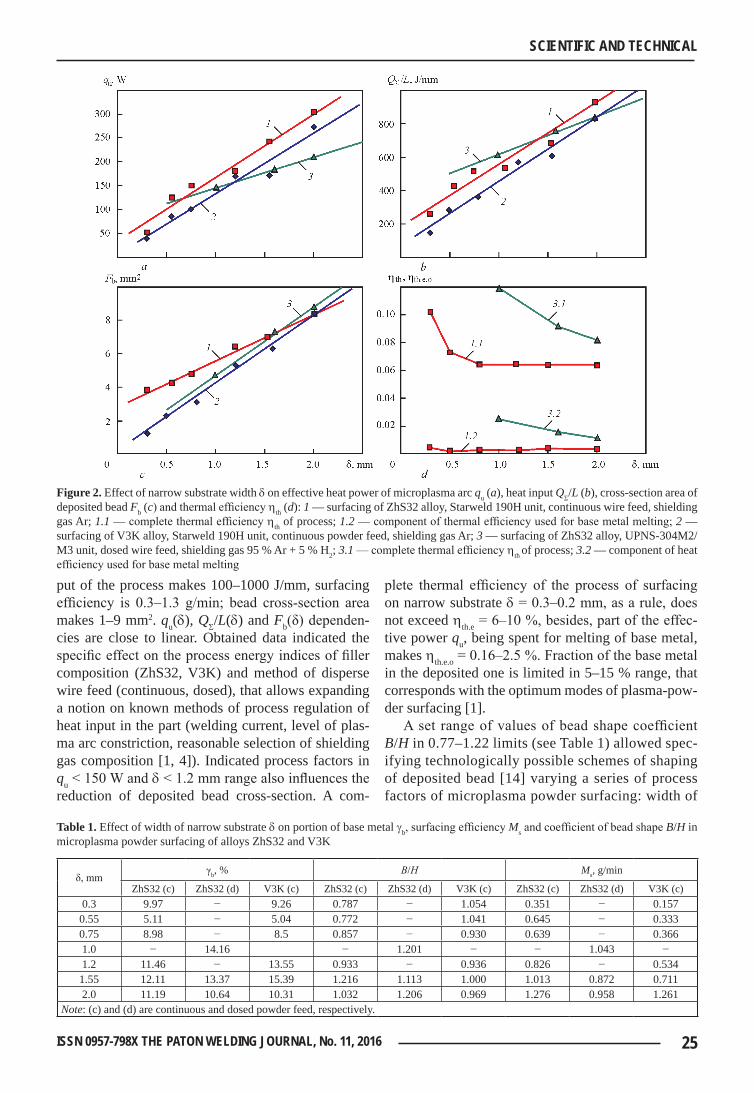
25ISSN 0957-798X THE PATON WELDING JOURNAL, No. 11, 2016
SCIENTIFIC AND TECHNICAL
put of the process makes 100–1000 J/mm, surfacing efficiency is 0.3–1.3 g/min; bead cross-section area makes 1–9 mm2. qu(d), QS/L(d) and Fb(δ) dependen-cies are close to linear. Obtained data indicated the specific effect on the process energy indices of filler composition (ZhS32, V3K) and method of disperse wire feed (continuous, dosed), that allows expanding a notion on known methods of process regulation of heat input in the part (welding current, level of plas-ma arc constriction, reasonable selection of shielding gas composition [1, 4]). Indicated process factors in qu < 150 W and d < 1.2 mm range also influences the reduction of deposited bead cross-section. A com-
plete thermal efficiency of the process of surfacing on narrow substrate d = 0.3–0.2 mm, as a rule, does not exceed hth.e = 6–10 %, besides, part of the effec-tive power qu, being spent for melting of base metal, makes hth.e.o = 0.16–2.5 %. Fraction of the base metal in the deposited one is limited in 5–15 % range, that corresponds with the optimum modes of plasma-pow-der surfacing [1].
A set range of values of bead shape coefficient B/H in 0.77–1.22 limits (see Table 1) allowed spec-ifying technologically possible schemes of shaping of deposited bead [14] varying a series of process factors of microplasma powder surfacing: width of
Figure 2. Effect of narrow substrate width d on effective heat power of microplasma arc qu (a), heat input QS/L (b), cross-section area of deposited bead Fb (c) and thermal efficiency hth (d): 1 — surfacing of ZhS32 alloy, Starweld 190H unit, continuous wire feed, shielding gas Ar; 1.1 — complete thermal efficiency hth of process; 1.2 — component of thermal efficiency used for base metal melting; 2 — surfacing of V3K alloy, Starweld 190H unit, continuous powder feed, shielding gas Ar; 3 — surfacing of ZhS32 alloy, UPNS-304M2/M3 unit, dosed wire feed, shielding gas 95 % Ar + 5 % H2; 3.1 — complete thermal efficiency hth of process; 3.2 — component of heat efficiency used for base metal melting
Table 1. Effect of width of narrow substrate d on portion of base metal gb, surfacing efficiency Ms and coefficient of bead shape B/H in microplasma powder surfacing of alloys ZhS32 and V3K
δ, mmγb, % В/Н Ms, g/min
ZhS32 (c) ZhS32 (d) V3K (c) ZhS32 (c) ZhS32 (d) V3K (c) ZhS32 (c) ZhS32 (d) V3K (c)0.3 9.97 − 9.26 0.787 − 1.054 0.351 − 0.157
0.55 5.11 − 5.04 0.772 − 1.041 0.645 − 0.3330.75 8.98 − 8.5 0.857 − 0.930 0.639 − 0.3661.0 − 14.16 − 1.201 − − 1.043 −1.2 11.46 − 13.55 0.933 − 0.936 0.826 − 0.534
1.55 12.11 13.37 15.39 1.216 1.113 1.000 1.013 0.872 0.7112.0 11.19 10.64 10.31 1.032 1.206 0.969 1.276 0.958 1.261
Note: (c) and (d) are continuous and dosed powder feed, respectively.
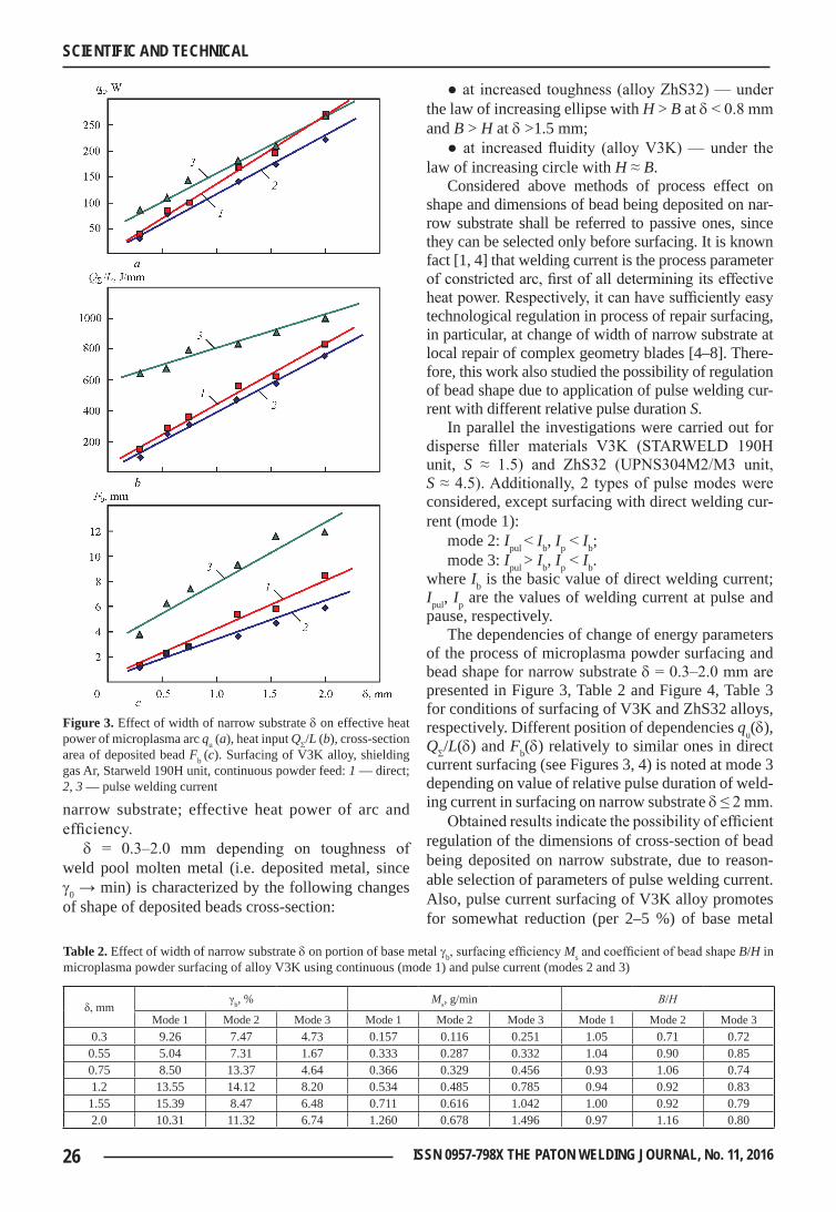
26 ISSN 0957-798X THE PATON WELDING JOURNAL, No. 11, 2016
SCIENTIFIC AND TECHNICAL
narrow substrate; effective heat power of arc and efficiency.
d = 0.3–2.0 mm depending on toughness of weld pool molten metal (i.e. deposited metal, since g0 → min) is characterized by the following changes of shape of deposited beads cross-section:
● at increased toughness (alloy ZhS32) — under the law of increasing ellipse with H > B at d < 0.8 mm and B > H at d >1.5 mm;
● at increased fluidity (alloy V3K) — under the law of increasing circle with H ≈ B.
Considered above methods of process effect on shape and dimensions of bead being deposited on nar-row substrate shall be referred to passive ones, since they can be selected only before surfacing. It is known fact [1, 4] that welding current is the process parameter of constricted arc, first of all determining its effective heat power. Respectively, it can have sufficiently easy technological regulation in process of repair surfacing, in particular, at change of width of narrow substrate at local repair of complex geometry blades [4–8]. There-fore, this work also studied the possibility of regulation of bead shape due to application of pulse welding cur-rent with different relative pulse duration S.
In parallel the investigations were carried out for disperse filler materials V3K (STARWELD 190H unit, S ≈ 1.5) and ZhS32 (UPNS304M2/M3 unit, S ≈ 4.5). Additionally, 2 types of pulse modes were considered, except surfacing with direct welding cur-rent (mode 1):
mode 2: Ipul < Ib, Ip < Ib;mode 3: Ipul > Ib, Ip < Ib.
where Ib is the basic value of direct welding current; Ipul, Ip are the values of welding current at pulse and pause, respectively.
The dependencies of change of energy parameters of the process of microplasma powder surfacing and bead shape for narrow substrate d = 0.3–2.0 mm are presented in Figure 3, Table 2 and Figure 4, Table 3 for conditions of surfacing of V3K and ZhS32 alloys, respectively. Different position of dependencies qu(d), QS/L(d) and Fb(d) relatively to similar ones in direct current surfacing (see Figures 3, 4) is noted at mode 3 depending on value of relative pulse duration of weld-ing current in surfacing on narrow substrate d ≤ 2 mm.
Obtained results indicate the possibility of efficient regulation of the dimensions of cross-section of bead being deposited on narrow substrate, due to reason-able selection of parameters of pulse welding current. Also, pulse current surfacing of V3K alloy promotes for somewhat reduction (per 2–5 %) of base metal
Figure 3. Effect of width of narrow substrate d on effective heat power of microplasma arc qu (a), heat input QS/L (b), cross-section area of deposited bead Fb (c). Surfacing of V3K alloy, shielding gas Ar, Starweld 190H unit, continuous powder feed: 1 — direct; 2, 3 — pulse welding current
Table 2. Effect of width of narrow substrate d on portion of base metal gb, surfacing efficiency Ms and coefficient of bead shape B/H in microplasma powder surfacing of alloy V3K using continuous (mode 1) and pulse current (modes 2 and 3)
δ, mmγb, % Ms, g/min В/Н
Mode 1 Mode 2 Mode 3 Mode 1 Mode 2 Mode 3 Mode 1 Mode 2 Mode 30.3 9.26 7.47 4.73 0.157 0.116 0.251 1.05 0.71 0.72
0.55 5.04 7.31 1.67 0.333 0.287 0.332 1.04 0.90 0.850.75 8.50 13.37 4.64 0.366 0.329 0.456 0.93 1.06 0.741.2 13.55 14.12 8.20 0.534 0.485 0.785 0.94 0.92 0.83
1.55 15.39 8.47 6.48 0.711 0.616 1.042 1.00 0.92 0.792.0 10.31 11.32 6.74 1.260 0.678 1.496 0.97 1.16 0.80
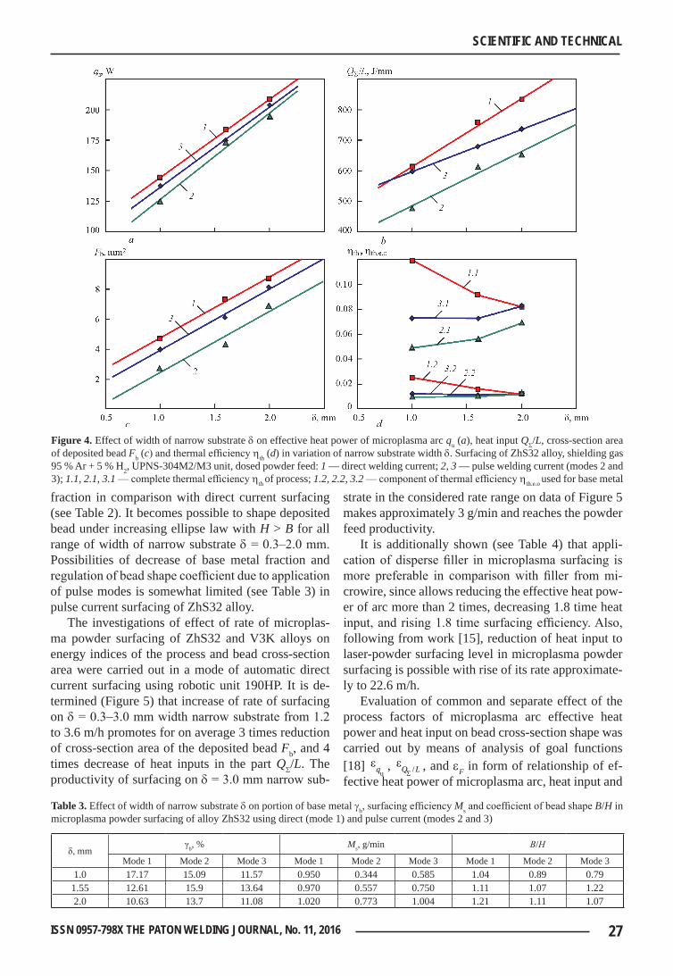
27ISSN 0957-798X THE PATON WELDING JOURNAL, No. 11, 2016
SCIENTIFIC AND TECHNICAL
fraction in comparison with direct current surfacing (see Table 2). It becomes possible to shape deposited bead under increasing ellipse law with H > B for all range of width of narrow substrate d = 0.3–2.0 mm. Possibilities of decrease of base metal fraction and regulation of bead shape coefficient due to application of pulse modes is somewhat limited (see Table 3) in pulse current surfacing of ZhS32 alloy.
The investigations of effect of rate of microplas-ma powder surfacing of ZhS32 and V3K alloys on energy indices of the process and bead cross-section area were carried out in a mode of automatic direct current surfacing using robotic unit 190HP. It is de-termined (Figure 5) that increase of rate of surfacing on d = 0.3–3.0 mm width narrow substrate from 1.2 to 3.6 m/h promotes for on average 3 times reduction of cross-section area of the deposited bead Fb, and 4 times decrease of heat inputs in the part QS/L. The productivity of surfacing on d = 3.0 mm narrow sub-
strate in the considered rate range on data of Figure 5 makes approximately 3 g/min and reaches the powder feed productivity.
It is additionally shown (see Table 4) that appli-cation of disperse filler in microplasma surfacing is more preferable in comparison with filler from mi-crowire, since allows reducing the effective heat pow-er of arc more than 2 times, decreasing 1.8 time heat input, and rising 1.8 time surfacing efficiency. Also, following from work [15], reduction of heat input to laser-powder surfacing level in microplasma powder surfacing is possible with rise of its rate approximate-ly to 22.6 m/h.
Evaluation of common and separate effect of the process factors of microplasma arc effective heat power and heat input on bead cross-section shape was carried out by means of analysis of goal functions [18]
uqe , /Q LSe , and eF in form of relationship of ef-
fective heat power of microplasma arc, heat input and
Figure 4. Effect of width of narrow substrate d on effective heat power of microplasma arc qu (a), heat input QS/L, cross-section area of deposited bead Fb (c) and thermal efficiency hth (d) in variation of narrow substrate width d. Surfacing of ZhS32 alloy, shielding gas 95 % Ar + 5 % H2, UPNS-304M2/M3 unit, dosed powder feed: 1 — direct welding current; 2, 3 — pulse welding current (modes 2 and 3); 1.1, 2.1, 3.1 — complete thermal efficiency hth of process; 1.2, 2.2, 3.2 — component of thermal efficiency hth.e.o used for base metal
Table 3. Effect of width of narrow substrate d on portion of base metal gb, surfacing efficiency Ms and coefficient of bead shape B/H in microplasma powder surfacing of alloy ZhS32 using direct (mode 1) and pulse current (modes 2 and 3)
δ, mmγb, % Ms, g/min В/Н
Mode 1 Mode 2 Mode 3 Mode 1 Mode 2 Mode 3 Mode 1 Mode 2 Mode 31.0 17.17 15.09 11.57 0.950 0.344 0.585 1.04 0.89 0.79
1.55 12.61 15.9 13.64 0.970 0.557 0.750 1.11 1.07 1.222.0 10.63 13.7 11.08 1.020 0.773 1.004 1.21 1.11 1.07
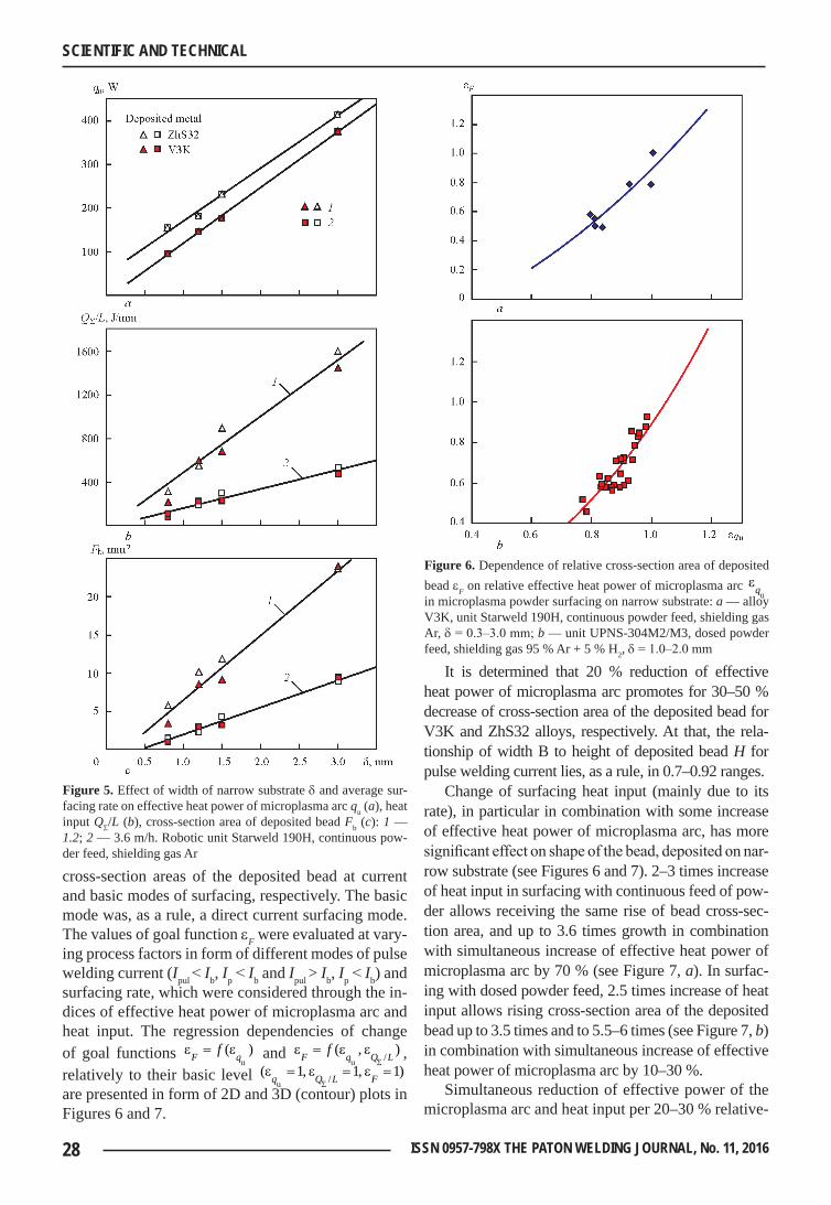
28 ISSN 0957-798X THE PATON WELDING JOURNAL, No. 11, 2016
SCIENTIFIC AND TECHNICAL
cross-section areas of the deposited bead at current and basic modes of surfacing, respectively. The basic mode was, as a rule, a direct current surfacing mode. The values of goal function eF were evaluated at vary-ing process factors in form of different modes of pulse welding current (Ipul < Ib, Ip < Ib and Ipul > Ib, Ip < Ib) and surfacing rate, which were considered through the in-dices of effective heat power of microplasma arc and heat input. The regression dependencies of change of goal functions ( )
uF qfe = e and /( , )uF q Q Lf
Se = e e ,
relatively to their basic level /( 1, 1, 1)uq Q L FS
e = e = e = are presented in form of 2D and 3D (contour) plots in Figures 6 and 7.
It is determined that 20 % reduction of effective heat power of microplasma arc promotes for 30–50 % decrease of cross-section area of the deposited bead for V3K and ZhS32 alloys, respectively. At that, the rela-tionship of width B to height of deposited bead H for pulse welding current lies, as a rule, in 0.7–0.92 ranges.
Change of surfacing heat input (mainly due to its rate), in particular in combination with some increase of effective heat power of microplasma arc, has more significant effect on shape of the bead, deposited on nar-row substrate (see Figures 6 and 7). 2–3 times increase of heat input in surfacing with continuous feed of pow-der allows receiving the same rise of bead cross-sec-tion area, and up to 3.6 times growth in combination with simultaneous increase of effective heat power of microplasma arc by 70 % (see Figure 7, a). In surfac-ing with dosed powder feed, 2.5 times increase of heat input allows rising cross-section area of the deposited bead up to 3.5 times and to 5.5–6 times (see Figure 7, b) in combination with simultaneous increase of effective heat power of microplasma arc by 10–30 %.
Simultaneous reduction of effective power of the microplasma arc and heat input per 20–30 % relative-
Figure 5. Effect of width of narrow substrate d and average sur-facing rate on effective heat power of microplasma arc qu (a), heat input QS/L (b), cross-section area of deposited bead Fb (c): 1 — 1.2; 2 — 3.6 m/h. Robotic unit Starweld 190H, continuous pow-der feed, shielding gas Ar
Figure 6. Dependence of relative cross-section area of deposited bead eF on relative effective heat power of microplasma arc
uqe in microplasma powder surfacing on narrow substrate: a — alloy V3K, unit Starweld 190H, continuous powder feed, shielding gas Ar, d = 0.3–3.0 mm; b — unit UPNS-304M2/M3, dosed powder feed, shielding gas 95 % Ar + 5 % H2, d = 1.0–2.0 mm
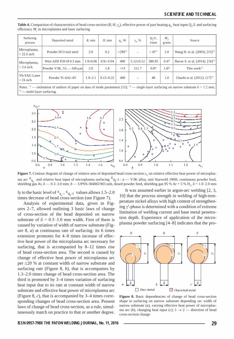
29ISSN 0957-798X THE PATON WELDING JOURNAL, No. 11, 2016
SCIENTIFIC AND TECHNICAL
ly to the basic level of uqe , /Q LS
e values allows 1.5–2.0 times decrease of bead cross-section (see Figure 7).
Analysis of experimental data, given in Fig-ures 2–7, allowed outlining 3 basic laws of change of cross-section of the bead deposited on narrow substrate of d = 0.5–3.0 mm width. First of them is caused by variation of width of narrow substrate (Fig-ure 8, a) at continuous rate of surfacing: its 6 times extension promotes for 4–8 times increase of effec-tive heat power of the microplasma arc necessary for surfacing, that is accompanied by 8–12 times rise of bead cross-section area. The second is caused by change of effective heat power of microplasma arc per ±20 % at constant width of narrow substrate and surfacing rate (Figure 8, b), that is accompanies by 1.3–2.0 times change of bead cross-section area. The third is promoted by 3–4 times variation of surfacing heat input due to its rate at constant width of narrow substrate and effective heat power of microplasma arc (Figure 8, c), that is accompanied by 3–4 times corre-sponding changes of bead cross-section area. Present laws of change of bead cross-section, as a rule, simul-taneously match on practice to that or another degree.
It was assumed earlier in argon-arc welding [2, 3, 10] that the process strength in welding of high-tem-perature nickel alloys with high content of strengthen-ing g′-phase is determined with a condition of extreme limitation of welding current and base metal penetra-tion depth. Experience of application of the micro-plasma powder surfacing [4–8] indicates that the pro-
Table 4. Comparison of characteristics of bead cross-section (B, H, gb), effective power of part heating qu, heat input QS/L and surfacing efficiency Ms in microplasma and laser surfacing
Surfacing process
Deposited metal В, mm Н, mm qu, W γb, %QΣ/L, J/mm
Ms, g/min
Source
Microplasma, ≈ 22.6 m/h Powder H13 tool steel 2.0 0.2 ≈280*1 – ≈ 45*1 1.0 Wang H. et al. (2003). [15]*3
Microplasma, ≈ 3.6 m/h
Wire AISI P20 Ø 0.3 mm 1.9±0.06 0.9± 0.04 400 5.12±0.12 380.95 0.47 Jhavar S. et al. (2014). [16]*3
Powder V3K, 53…–160 mm 2.0 1.8 ≈15 211.7 0.87 1.87 This work*2
Yb:YAG Laser ≈ 24 m/h Powder Ti–6Al–4V 1.9–2.1 0.15–0.22 400 – 48 1.0 Gharbi et al. (2012). [17]*3
Notes. *1 — estimation of authors of paper on data of mode parameters [15]; *2 — single-layer surfacing on narrow substrate d = 1.2 mm; *3 — multi-layer surfacing.
Figure 7. Contour diagram of change of relative area of deposited bead cross-section eF on relative effective heat power of microplas-ma arc
uqe and relative heat input of microplasma surfacing /Q LSe : a — V3K alloy, unit Starweld 190H, continuous powder feed,
shielding gas Ar, d — 0.3–3.0 mm; b — UPNS-304M2/M3 unit, dosed powder feed, shielding gas 95 % Ar + 5 % H2, d = 1.0–2.0 mm
Figure 8. Basic dependencies of change of bead cross-section shape in surfacing on narrow substrate depending on: width of narrow substrate (a), varying effective heat power of microplas-ma arc (b), changing heat input (c); 1 → 2 — direction of bead cross-section change
30 ISSN 0957-798X THE PATON WELDING JOURNAL, No. 11, 2016
SCIENTIFIC AND TECHNICAL
cess strength in single-layer surfacing of blade edges can be provided in sufficiently wide range of mode parameters (I = 2–35 A, v = 0.2–5.0 m/h, Fb < 30–35 mm2), where the base metal penetration depth, as a rule, does not exceed 1 mm.
Analysis of corresponding modes of surfacing on narrow substrate d ≤ 3 mm, which are supposed to be close to optimum, showed that 2–4 times change of cross-section area of a bead being deposited promotes for insignificant variation of portion of base metal in the deposited one and it does not exceed 15 %. Re-spectively, portion of heat consumed for base metal melting does not exceed 2.5 % of effective heat pow-er of the microplasma arc. Therefore, it is relevant to formulate additional criteria of the process strength at transfer to multi-layer surfacing of the blade edges.
A surfacing heat input can be such an additional cri-terion of the process strength based on stated in works [11, 14] relationship of tendency to crack formation for considered welded joints and total heat input in the part as well as stated in this work dependencies of reg-ulation of cross-section of the deposited bead. Thus, cross-section area of the deposited layer in multi-layer surfacing shall be selected taking into account heat in-put for determination of narrow substrate width.
Conclusions
1. Process range of energy indices was specified for single-layer microplasma powder surfacing on nar-row substrate of width less than 3 mm. In keeping with other technological recommendations, it is pos-sible to provide the process strength of welded joint «base-deposited metal», in which at least one of the materials is high-temperature nickel alloy containing more than 55 vol.% of g′-phase, using 30–420 W ef-fective heat power of microplasma arc; 100–1600 J/mm surfacing heat input; 0.3–3.0 g/min surfacing ef-ficiency; 1–25 mm2 deposited bead cross-section area.
2. In this case under conditions of limited base metal penetration depth, the process regulation of shape and size of cross-section of deposited bead can be done by means of change of effective heat power of the microplasma arc, surfacing heat input, reasonable selection of deposited metal composition and powder feed method (dosed, continuous).The most efficient among them at constant width of narrow substrate are 2.5–4 times variation of heat input, 30–50 % change of effective heat power of the microplasma arc as well as 3.5–6 times variation at their combination. Detect-ed dependencies of the bead shape regulation are used at JSC «Motor Sich» under conditions of serial repair of GTE blades.
3. Additional criteria of the process strength in repair multi-layer microplasma powder surfacing of
blade edges of high-temperature nickel alloys can be the value of heat input and related with it height and cross-section area of the deposited metal layer.
1. Gladky, P.V., Pereplyotchikov, E.F., Ryabtsev, I.A. (2007) Plasma surfacing. Kiev: Ekotekhnologiya.
2. Peremilovsky, I.A., Gejchenko, V.S., Frumin, I.I. (1976) Sur-facing repair of turbine blades of aircraft engines. Avtomatich. Svarka, 5, 54–56.
3. Petrik, I.A., Peremilovsky, I.A. (2001) Further development of technology for hardening of flange platform faces of tur-bine blades from high-temperature alloys. Tekhnologicheskie Sistemy, 3, 90–92.
4. Yarovytsyn, O.V. (2009) Microplasma powder surfacing of high-temperature nickel alloys containing 45–65 % of g´-phase: Syn. of Thesis for Cand. of Techn. Sci. Degree. Kiev: PWI.
5. (2010) Technological Seminar Deloro Stellite in Zaporozhie. The Paton Welding J., 1, 46–49.
6. Yushchenko, K.A., Savchenko, V.S., Yarovitsyn, A.V. et al. (2010) Development of the technology for repair microplas-ma powder cladding of flange platform faces of aircraft en-gine high-pressure turbine blades. Ibid., 8, 21–24.
7. Yushchenko, K.A., Yarovitsyn, A.V. (2012) Improvement of technology of repair of upper flange platform faces of aircraft engine blades. In: Complex Program of NASU on Problems of Service Life and Service Safety of Constructions, Structures and Machines. Transact. on Results of 2010–2012. Kiev: PWI.
8. Zhemanyuk, P.D., Petrik, I.A., Chigilejchik, S.L. (2015) Expe-rience of introduction of the technology of reconditioning mi-croplasma powder surfacing at repair of high-pressure turbine blades in batch production. The Paton Welding J., 8, 39–42.
9. Boguslaev, V.A., Muravchenko, V.M., Zhemanyuk, P.D. et al. (2003) Technological support of service characteristics of gas turbine engine parts. Turbine blades. Pt 2. Zaporozhie: JSC Motor Sich.
10. Sorokin, L.I., Lukin, V.I., Bagdasarov, Yu.S. (1997) Weldabil-ity of cast high-temperature alloys of ZhS6 type. Svarochn. Proizvodstvo, 6, 12–17.
11. Yarovitsyn, A.V. (2015) Energy approach in analysis of mi-croplasma powder surfacing modes. The Paton Welding J., 5/6, 22–25.
12. Popov, S.A. (1987) Grinding operations. Moscow: Vysshaya Shkola.
13. Kondratyuk, E.V., Leontiev, V.A., Shusha, A.V. et al. (2013) Profile deep grinding of gas turbine engine parts. Promyshlen-nost v Fokuse, 5, 22–24.
14. Yushchenko, K.A., Yarovitsyn, A.V., Khrushchov, G.D. et al. (2015) Analysis of process of bead shaping in cladding on narrow substrate. The Paton Welding J., 9, 20–27.
15. Wang, H., Jiang, W., Vallant, M. et al. (2003) Microplasma powder deposition as a new solid freeform fabrication pro-cess. Proc. Inst. Mech. Engrs., 217(Pt B.J.), 1641–1650.
16. Suyog Jhavar, Jain, N.K., Paul, C.P. (2014) Development of microplasma transferred arc (µ-PTA) wire deposition process for additive layer manufacturing applications. J. of Materials Processing Technology, 214(5), 1102–1110.
17. Gharbi, M., Peyre P., Gorny, C. et al. (2012) Influence of var-ious process conditions on surface finishes induced by direct metal deposition laser technique on a Ti–6Al–4V alloy. Ibid., 213(5), 791–800.
18. (1988) Mathematical dictionary. Ed. by Yu.V. Prokhorov. Moscow: Sovremennaya Encyclopediya.
Received 06.07.2016

31ISSN 0957-798X THE PATON WELDING JOURNAL, No. 11, 2016
SCIENTIFIC AND TECHNICAL
doi.org/10.15407/tpwj2016.11.05
EFFECT OF LASER RADIATION ABSORPTION ON EFFICIENCY OF LASER WELDING OF COPPER AND ITS ALLOYSV.Yu. KHASKIN1, 2, V.N. KORZHIK1, 2, T.G. CHIZHSKAYA3, V.N. SIDORETS2 and LO ZIE1
1Guangdong Welding Institute (Chinese-Ukrainian E. O. Paton Institute of Welding) Guangzhou, China 2E.O. Paton Electric Welding Institute, NASU
11 Kazimir Malevich Str., 03680, Kiev, Ukraine. E-mail: [email protected] 3NTUU «Igor Sikorsky Kyiv Polytechnic Institute»
37 Pobedy Ave., Kiev-56, Ukraine
Due to a high reflection power of copper it is usually assumed that the laser welding of products of this material is not rational. However, in the modern industry the problems of joining the parts of copper and its alloys periodically arise, applying narrow welds with a deep vapor-gas channel. Moreover, for technical reasons the use of electron beam weld-ing is not always possible and a sufficiently wide availability of fiber (wavelength of 1.07 mm) and disc (wavelength of 1.03 mm) industrial lasers of the latest generation makes the problem of laser welding of these materials challeng-ing. Therefore, the aim of the work was to study the conditions of absorbing the laser radiation with the wavelength of 1.03–1.07 mm by copper and its alloys in laser welding with a deep penetration, as well as to determine the basic parameters of the welding mode and to evaluate the process effectiveness. It was shown in the work that for certain combinations of thickness of copper alloy and density of radiation power with the wavelength of 1.03–1.07 mm, the optimal speed of welding process exists, at which its technical and economic efficiency is maximum. This speed should be such that the absorbing capacity (integrated over the spot of laser heating) can be at the level of about 13–15 %. The exceeding of welding speed leads to a sharp decrease in absorbing capacity, and, consequently, to the need in increasing the radiation power and growing the cost of the process. The decrease in welding speed relatively to the optimal one leads to decrease in efficiency, overheating of metal in the weld pool and to such defects of weld shaping, as sagging and metal splashes. 11 Ref., 8 Figures.
K e y w o r d s : laser welding, copper, solid-state laser radiation, absorbing factor, radiation power, welding speed
One of the challenging problems of the modern sci-ence and engineering in the field of fusion welding of metals is the creation of new power sources, which provide the control of concentration of heat energy introduced to the metal during welding process. This ultimately allows providing the required efficiency of welding, quality of the produced welded joint, process stability and reproduction of its results. In the recent decades in capacity of such controllable heat power source for welding of metallic materials a high-con-centrated laser source is ever widely applied, which is realized by thermal effect of the focused laser beam on metal being welded [1].
However, until now the regularities of influence of laser heat source on some metallic materials were studied insufficiently. In particular, such materials in-clude copper and its alloys. Due to a high reflection power of copper it is usually assumed that the laser welding of products of this material is not rational. However, in the modern industry the problems of joining the parts of copper and its alloys periodically arise, applying narrow welds with a deep vapor-gas channel. Moreover, for technical reasons the use of electron beam welding is not always possible and a
sufficiently wide availability of fiber (wavelength of 1.07 mm) and disc (wavelength of 1.03 mm) industrial lasers of the latest generation makes the problem of laser welding of these materials challenging [2].
To solve this problem it is necessary to carry out investigation of physics of the process of effect of laser heat power source on welded metal, having the high thermal conductivity and reflection power, which is copper and its alloys, to develop the appropriate math-ematical models and to perform computer modeling of the mentioned process. Moreover, it is rational to eval-uate the efficiency of the process of laser welding of such materials by determination of basic mode param-eters, i.e. the necessary consumption of radiation power for welding at the corresponding speed.
Therefore, the aim of the work is the study of conditions of absorbing the laser radiation with the wavelength of 1.03–1.07 mm by copper and its alloys in laser welding with a deep penetration, as well as the determination of the basic parameters of welding mode and evaluation of the process efficiency.
Laser welding is characterized by the formation of a vapor-gas channel in the metal being welded. In [2] the behavior of the channel during welding is de-
© V.Yu. KHASKIN, V.N. KORZHIK, T.G. CHIZHSKAYA, V.N. SIDORETS and LO ZIE, 2016
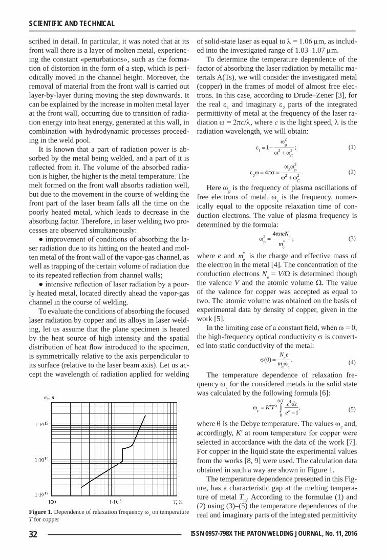
32 ISSN 0957-798X THE PATON WELDING JOURNAL, No. 11, 2016
SCIENTIFIC AND TECHNICAL
scribed in detail. In particular, it was noted that at its front wall there is a layer of molten metal, experienc-ing the constant «perturbations», such as the forma-tion of distortion in the form of a step, which is peri-odically moved in the channel height. Moreover, the removal of material from the front wall is carried out layer-by-layer during moving the step downwards. It can be explained by the increase in molten metal layer at the front wall, occurring due to transition of radia-tion energy into heat energy, generated at this wall, in combination with hydrodynamic processes proceed-ing in the weld pool.
It is known that a part of radiation power is ab-sorbed by the metal being welded, and a part of it is reflected from it. The volume of the absorbed radia-tion is higher, the higher is the metal temperature. The melt formed on the front wall absorbs radiation well, but due to the movement in the course of welding the front part of the laser beam falls all the time on the poorly heated metal, which leads to decrease in the absorbing factor. Therefore, in laser welding two pro-cesses are observed simultaneously:
● improvement of conditions of absorbing the la-ser radiation due to its hitting on the heated and mol-ten metal of the front wall of the vapor-gas channel, as well as trapping of the certain volume of radiation due to its repeated reflection from channel walls;
● intensive reflection of laser radiation by a poor-ly heated metal, located directly ahead the vapor-gas channel in the course of welding.
To evaluate the conditions of absorbing the focused laser radiation by copper and its alloys in laser weld-ing, let us assume that the plane specimen is heated by the heat source of high intensity and the spatial distribution of heat flow introduced to the specimen, is symmetrically relative to the axis perpendicular to its surface (relative to the laser beam axis). Let us ac-cept the wavelength of radiation applied for welding
of solid-state laser as equal to l = 1.06 mm, as includ-ed into the investigated range of 1.03–1.07 mm.
To determine the temperature dependence of the factor of absorbing the laser radiation by metallic ma-terials A(Ts), we will consider the investigated metal (copper) in the frames of model of almost free elec-trons. In this case, according to Drude–Zener [3], for the real e1 and imaginary e2 parts of the integrated permittivity of metal at the frequency of the laser ra-diation w = 2pc/l, where с is the light speed, l is the radiation wavelength, we will obtain:
2
2 21 1 ;p
C
we = −
w + w
(1)
2
2 22 4 .pñ
C
w we w = ps =
w + w
(2)
Here wp is the frequency of plasma oscillations of free electrons of metal, wc is the frequency, numer-ically equal to the opposite relaxation time of con-duction electrons. The value of plasma frequency is determined by the formula:
2*
4;e
pe
neN
m
pw =
(3)
where e and *e
m is the charge and effective mass of the electron in the metal [4]. The concentration of the conduction electrons Ne = V/W is determined though the valence V and the atomic volume W. The value of the valence for copper was accepted as equal to two. The atomic volume was obtained on the basis of experimental data by density of copper, given in the work [5].
In the limiting case of a constant field, when w = 0, the high-frequency optical conductivity s is convert-ed into static conductivity of the metal:
(0) .e
e c
N ems =
w
(4)
The temperature dependence of relaxation fre-quency wc for the considered metals in the solid state was calculated by the following formula [6]:
/ 45
0
,1
T
zcz dzK Te
q
′w =−∫
(5)
where q is the Debye temperature. The values wc and, accordingly, K′ at room temperature for copper were selected in accordance with the data of the work [7]. For copper in the liquid state the experimental values from the works [8, 9] were used. The calculation data obtained in such a way are shown in Figure 1.
The temperature dependence presented in this Fig-ure, has a characteristic gap at the melting tempera-ture of metal Tm. According to the formulae (1) and (2) using (3)–(5) the temperature dependences of the real and imaginary parts of the integrated permittivity Figure 1. Dependence of relaxation frequency wc on temperature
T for copper
33ISSN 0957-798X THE PATON WELDING JOURNAL, No. 11, 2016
SCIENTIFIC AND TECHNICAL
for copper at the frequency of solid-state laser radia-tion (l = 1.06 mm) were plotted, shown in Figure 2 (here and further, the temperature is expressed in Kel-vin degrees).
For the further calculations it is convenient to in-troduce the real n and imaginary k parts of the com-plex refractive index of metal at the frequency of laser radiation
1 2i n ike = e + e = +
(6)
using the following formulae for this:
2 21 2 1 ,2n
e + e + e=
(7)
2 21 2 1 .2k
e + e − e=
(8)
The temperature dependences of the real and imag-inary parts of the complex refractive index for copper are shown in Figure 3.
Using the obtained values n and k, let us determine the laser absorbing factor, normally falling on the plane metal surface (absorbing capacity), according to the known formula
2 2
4 .(1 )
nAn k
=+ +
(9)
In some cases the more important parameter is the reflection factor (reflectance), which can be deter-mined according to the formula
2 2
2 2(1 )1 .(1 )
n kR An k
− += − =
+ + (10)
Figure 4 shows the results of calculations of tem-perature dependences of the absorbing factor of radi-ation of solid-state laser for copper in the range from room to boiling temperatures of metal Tb and higher.
The calculation dependence of absorbing capac-ity, obtained for the selected type of radiation, was compared with the available experimental data [6–9] and the matching was quite satisfactory. According to the dependence, shown in Figure 5, to achieve the maximum values of absorbing factor of the surface
of the welded copper alloy in the zone of acting laser radiation with the wavelength of 1.06 mm, it should be heated to boiling temperature Тb. However, even heating to melting temperature Tm is sufficient for an abrupt jumpy increase in absorbing capacity from 2.0–2.5 to 4.5–5.0 %.
To determine the temperature distributions in the depth and on the surface of the copper specimen welded using focused laser radiation, the calculation using the method of finite differences was conduct-ed involving an implicit difference scheme. For this purpose the software product of the own development was applied, based on the computational and experi-mental methods, described in the work [10]. During calculations the thermophysical characteristics of copper were used given in the work [11]. The data obtained in the process of computer modeling were compared with the experimental results. While con-ducting the latter, the disc laser of the model TruDisk 10002 (company TRUMPF, Germany) was applied with the capacity of up to 10.0 KW. To move the weld-ing head, the robot of the model KR 60 HA (the com-pany KUKA, Germany) was used. Welding of speci-mens of copper of the type M1 of size 100×50×3 mm was performed in argon shielding with deposition and
Figure 2. Dependences of real e1 and imaginary e2 parts of inte-grated permittivity of copper on temperature T at frequency of radiation of solid-state laser (l = 1.06 mm)
Figure 3. Dependences of real n and imaginary k part of the inte-grated refractive index of copper on temperature T at frequency of radiation of solid-state laser (l = 1.06 mm)
Figure 4. Dependences of absorbing capacity A of copper on tem-perature T for radiation with wavelength of 1.06 mm
34 ISSN 0957-798X THE PATON WELDING JOURNAL, No. 11, 2016
SCIENTIFIC AND TECHNICAL
butt welds at the density of laser radiation power of 4.5∙107 W/cm2.
The investigations show that for the fixed thick-ness of penetrated specimen (in this case d = 3 mm) it is possible to select such welding speed vopt at which not more than one third of the length of heat source (i.e. diameter of laser radiation) acts constantly on the solid surface of copper, located directly ahead the vapor-gas channel during welding. In this region the absorbing capacity of the surface A changes from 2.0 to 5.0 %. Approximately two thirds of the length of the heat source (i.e. diameter of laser radiation) will fall in this case to the vapor-gas channel, the tempera-ture in which reaches not lower than 2900 K, and the absorbing capacity is 19–20 %. Such welding speed
amounts to about vopt ≤ 25 mm/s (90 m/h). It provides the absorbing capacity in the range of 13–15 % inte-grated on the spot of laser heating. In this case, the penetration depth will amount to not less than 3 mm (see Figure 5).
With increase in welding speed vw ≥ vopt the volume of laser power, falling to the region of a low absorbing capacity, will increase and a part of this energy, falling to the region with a high absorbing capacity, on the contrary, will decrease. This will result in decrease of integrated absorbing capacity of less than 13 % and, consequently, in need of increasing the laser radiation power. The last moment will result in increase in the cost of running meter of weld and the corresponding decrease in technical and economic efficiency of the
Figure 5. Distribution of temperatures T on the surface (a) and in the depth (b) of copper plate of 5 mm thickness in laser welding using radiation of solid-state laser (A = 13 %) with density of power 4.5∙107∙W/cm2 and speed vw = 90 m/h (25 mm/s)
Figure 6. Distribution of temperatures T on the surface (a) and in the depth (b) of copper plate of 5 mm thickness in laser welding using radiation of solid-state laser (A = 10 %) with density of power 4.5∙107 W/cm2 and speed vw = 120 m/h (33.3 mm/s)
Figure 7. Distribution of temperatures T on the surface (a) and in the depth (b) of copper plate of 5 mm thickness in laser welding using radiation of solid-state laser (A = 17 %) with density of power 4.5∙107 W/cm2 and speed vw = 60 m/h (16.7 mm/s)

35ISSN 0957-798X THE PATON WELDING JOURNAL, No. 11, 2016
SCIENTIFIC AND TECHNICAL
process. In this case, the penetration depth is much smaller than the required 3 mm, which will lead to the lack of penetration (Figure 6).
With decrease in welding speed relatively to the selected one (vw ≤ vopt) the greater part of radiation will fall to the vapor-gas channel, and absorbing capacity will increase by more than 15 %. Howev-er, in this case the process efficiency will decrease (vw ≤ 16.7 mm/s or vw ≤ 60 m/h), and it will become less effective. In this case, the penetration depth will significantly exceed the required 3 mm, which will re-sult in such shaping defects as sagging and splashes of the weld metal (Figure 7).
To perform the experimental verification of the predicted results of laser welding on plane specimens the surfacing welds were produced, then the penetra-tion depth was measured on macrosections and com-pared with the calculation data. In addition, at the calculation modes the butt joints were welded (Fig-ure 8). Such verification allowed establishing that the calculation accuracy amounts to about 5–8 %, which in the case of technological calculations is a satisfac-tory indicator.
Thus, the study of conditions of absorbing the la-ser radiation with the wavelength of 1.03–1.07 mm in welding with deep penetration of copper and its alloys allows stating that for a certain combination of welding material thickness and density of radia-tion power, such an optimal process speed exists, at which its technical and economic efficiency is max-imum. This speed corresponds to the integrated one over the spot of laser heating of absorbing capacity of about 13–15 %. The exceeding of welding speed leads to a sharp decrease in absorbing capacity, and, consequently, to the need in increasing the radiation power and growing of the process cost. The decrease in welding speed relatively to the optimal one leads to the decrease in efficiency, overheating of metal in the weld pool and to such defects of weld shaping, as sagging and metal splashes.
The work was carried out at the support of the For-eign Experts Program of China No. WQ20124400119,
Program of the Innovation Group of the Prov-ince Guangdong, China No. 201101С0104901263, Guangdong research Project No. 2015А050502039, Guangdong research Project No. 2016В050501002.
1. Grigoryants, A.G., Shiganov, I.N. (1988) Laser equipment and technology. Book 5: Laser welding of metals. Manual for inst. of higher education. Ed. by A.G. Grigoryants. Moscow: Vysshaya Shkola.
2. Bernadsky, V.N., Shelyagin, V.D., Makovetskaya, O.K. (2007) Present market of laser equipment for welding and processing of materials. The Paton Welding J., 10, 44–49.
3. Noskov, M.M. (1983) Optical and magnetooptical properties of metals. Sverdlovsk: UNTs AN SSSR.
4. Kiselev, A.I., Akashev, L.A., Kononenko, V.I. (2004) Effec-tive mass of electrons in melts of aluminium, cesium and Al–3 at.% Ce binary system. Zh. Tekhnicheskoj Fiziki, 74(Is-sue 3), 20–23.
5. Zinoviev, V.E. (1989) Thermophysical properties of metals at high temperatures: Refer. Book. Moscow: Metallurgiya.
6. Ujihara, K. (1972) Reflectivity of metals at high temperatures. J. of Applied Physics, 43(5), 2376–2383.
7. Ordal, M.A., Long, L.L., Bell, R.J. et al. (1983) Optical prop-erties of the metals Al, Co, Cu, Au, Fe, Pb, Ni, Pd, Pt, Ag, Ti and W in the infrared and far infrared. Applied Optics, 22(7), 1099–1119.
8. Miller, J. (1969) Optical properties of liquid metals at high temperatures. Phil. Mag., Vol. 20, 12(Issue 168), 1115–1132.
9. Comins, N.R. (1972) The optical properties of liquid metals. Ibid., 25(Issue 4), 817–831.
10. Khaskin, V.Yu. (2012) Experiment-calculated method for de-termination of conditions of laser surfacing processes. Nauka ta Innovatsii, 8(6), 5–16.
Received 11.10.2016
Figure 8. Butt joint of sheet copper M1 (d = 3 mm) produced by laser welding in argon using radiation of power density 4.5∙107 W/cm2 and speed vw = 90 m/h (25 mm/s): a — top; b — bottom
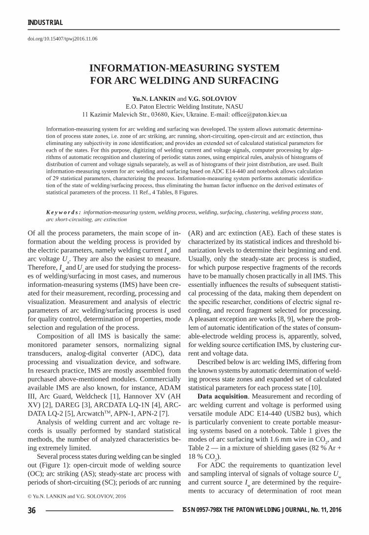
36 ISSN 0957-798X THE PATON WELDING JOURNAL, No. 11, 2016
INDUSTRIAL
doi.org/10.15407/tpwj2016.11.06
INFORMATION-MEASURING SYSTEM FOR ARC WELDING AND SURFACING
Yu.N. LANKIN and V.G. SOLOVIOVE.O. Paton Electric Welding Institute, NASU
11 Kazimir Malevich Str., 03680, Kiev, Ukraine. E-mail: [email protected]
Information-measuring system for arc welding and surfacing was developed. The system allows automatic determina-tion of process state zones, i.e. zone of arc striking, arc running, short-circuiting, open-circuit and arc extinction, thus eliminating any subjectivity in zone identification; and provides an extended set of calculated statistical parameters for each of the states. For this purpose, digitizing of welding current and voltage signals, computer processing by algo-rithms of automatic recognition and clustering of periodic status zones, using empirical rules, analysis of histograms of distribution of current and voltage signals separately, as well as of histograms of their joint distribution, are used. Built information-measuring system for arc welding and surfacing based on ADC E14-440 and notebook allows calculation of 29 statistical parameters, characterizing the process. Information-measuring system performs automatic identifica-tion of the state of welding/surfacing process, thus eliminating the human factor influence on the derived estimates of statistical parameters of the process. 11 Ref., 4 Tables, 8 Figures.
K e y w o r d s : information-measuring system, welding process, welding, surfacing, clustering, welding process state, arc short-circuiting, arc extinction
Of all the process parameters, the main scope of in-formation about the welding process is provided by the electric parameters, namely welding current Iw and arc voltage Ua. They are also the easiest to measure. Therefore, Iw and Ua are used for studying the process-es of welding/surfacing in most cases, and numerous information-measuring systems (IMS) have been cre-ated for their measurement, recording, processing and visualization. Measurement and analysis of electric parameters of arc welding/surfacing process is used for quality control, determination of properties, mode selection and regulation of the process.
Composition of all IMS is basically the same: monitored parameter sensors, normalizing signal transducers, analog-digital converter (ADC), data processing and visualization device, and software. In research practice, IMS are mostly assembled from purchased above-mentioned modules. Commercially available IMS are also known, for instance, ADAM III, Arc Guard, Weldcheck [1], Hannover XV (AH XV) [2], DAREG [3], ARCDATA LQ-1N [4], ARC-DATA LQ-2 [5], ArcwatchTM, APN-1, APN-2 [7].
Analysis of welding current and arc voltage re-cords is usually performed by standard statistical methods, the number of analyzed characteristics be-ing extremely limited.
Several process states during welding can be singled out (Figure 1): open-circuit mode of welding source (OC); arc striking (AS); steady-state arc process with periods of short-circuiting (SC); periods of arc running
(AR) and arc extinction (AE). Each of these states is characterized by its statistical indices and threshold bi-narization levels to determine their beginning and end. Usually, only the steady-state arc process is studied, for which purpose respective fragments of the records have to be manually chosen practically in all IMS. This essentially influences the results of subsequent statisti-cal processing of the data, making them dependent on the specific researcher, conditions of electric signal re-cording, and record fragment selected for processing. A pleasant exception are works [8, 9], where the prob-lem of automatic identification of the states of consum-able-electrode welding process is, apparently, solved, for welding source certification IMS, by clustering cur-rent and voltage data.
Described below is arc welding IMS, differing from the known systems by automatic determination of weld-ing process state zones and expanded set of calculated statistical parameters for each process state [10].
Data acquisition. Measurement and recording of arc welding current and voltage is performed using versatile module ADC E14-440 (USB2 bus), which is particularly convenient to create portable measur-ing systems based on a notebook. Table 1 gives the modes of arc surfacing with 1.6 mm wire in CO2, and Table 2 — in a mixture of shielding gases (82 % Ar + 18 % CO2).
For ADC the requirements to quantization level and sampling interval of signals of voltage source Uw and current source Iw are determined by the require-ments to accuracy of determination of root mean
© Yu.N. LANKIN and V.G. SOLOVIOV, 2016
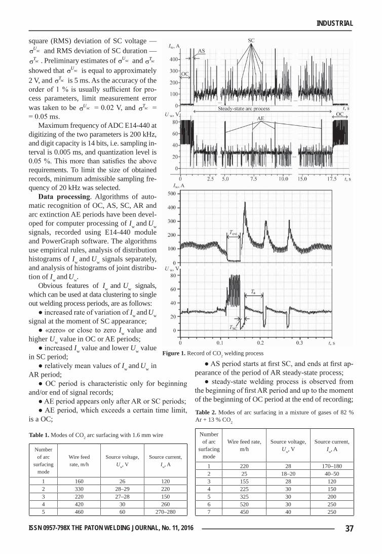
37ISSN 0957-798X THE PATON WELDING JOURNAL, No. 11, 2016
INDUSTRIAL
square (RMS) deviation of SC voltage — scUs and RMS deviation of SC duration — scTs . Preliminary estimates of scUs and scTs
showed that scUs is equal to approximately 2 V, and scTs is 5 ms. As the accuracy of the order of 1 % is usually sufficient for pro-cess parameters, limit measurement error was taken to be scUs = 0.02 V, and scTs = = 0.05 ms.
Maximum frequency of ADC E14-440 at digitizing of the two parameters is 200 kHz, and digit capacity is 14 bits, i.e. sampling in-terval is 0.005 ms, and quantization level is 0.05 %. This more than satisfies the above requirements. To limit the size of obtained records, minimum admissible sampling fre-quency of 20 kHz was selected.
Data processing. Algorithms of auto-matic recognition of OC, AS, SC, AR and arc extinction AE periods have been devel-oped for computer processing of Iw and Uw signals, recorded using E14-440 module and PowerGraph software. The algorithms use empirical rules, analysis of distribution histograms of Iw and Uw signals separately, and analysis of histograms of joint distribu-tion of Iw and Uw.
Obvious features of Iw and Uw signals, which can be used at data clustering to single out welding process periods, are as follows:
● increased rate of variation of Iw and Uw signal at the moment of SC appearance;
● «zero» or close to zero Iw value and higher Uw value in OC or AE periods;
● increased Iw value and lower Uw value in SC period;
● relatively mean values of Iw and Uw in AR period;
● OC period is characteristic only for beginning and/or end of signal records;
● AE period appears only after AR or SC periods;● AE period, which exceeds a certain time limit,
is a OC;
● AS period starts at first SC, and ends at first ap-pearance of the period of AR steady-state process;
● steady-state welding process is observed from the beginning of first AR period and up to the moment of the beginning of OC period at the end of recording;
Figure 1. Record of CO2 welding process
Table 1. Modes of CO2 arc surfacing with 1.6 mm wire
Number of arc
surfacing mode
Wire feed rate, m/h
Source voltage, Uw, V
Source current, Iw, A
1 160 26 1202 330 28–29 2203 220 27–28 1504 420 30 2605 460 60 270–280
Table 2. Modes of arc surfacing in a mixture of gases of 82 % Ar + 13 % CO2
Number of arc
surfacing mode
Wire feed rate, m/h
Source voltage, Uw, V
Source current, Iw, A
1 220 28 170–1802 25 18–20 40–503 155 28 1204 225 30 1505 325 30 2006 520 30 2507 450 40 250
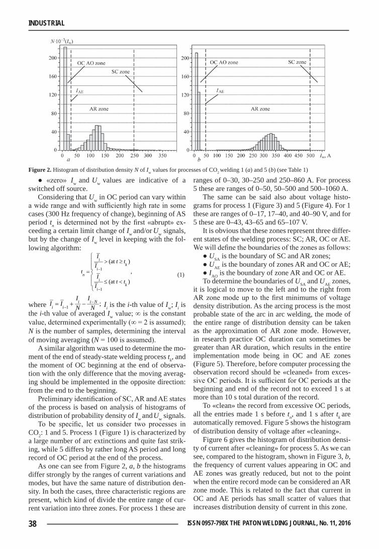
38 ISSN 0957-798X THE PATON WELDING JOURNAL, No. 11, 2016
INDUSTRIAL
● «zero» Iw and Uw values are indicative of a switched off source.
Considering that Uw in OC period can vary within a wide range and with sufficiently high rate in some cases (300 Hz frequency of change), beginning of AS period tn is determined not by the first «abrupt» ex-ceeding a certain limit change of Iw and/or Uw signals, but by the change of Iw level in keeping with the fol-lowing algorithm:
1
1
(at )
,
(at )
ik
in
ik
i
It t
It
It t
I
−
−
> ≥
=
≤ <
(1)
where 1 ;i i Ni i
I II I N N
−−
= + − Ii is the i-th value of Iw; Ii is the i-th value of averaged Iw value; ∞ is the constant value, determined experimentally (∞ = 2 is assumed); N is the number of samples, determining the interval of moving averaging (N = 100 is assumed).
A similar algorithm was used to determine the mo-ment of the end of steady-state welding process tk, and the moment of OC beginning at the end of observa-tion with the only difference that the moving averag-ing should be implemented in the opposite direction: from the end to the beginning.
Preliminary identification of SC, AR and AE states of the process is based on analysis of histograms of distribution of probability density of Iw and Uw signals.
To be specific, let us consider two processes in CO2: 1 and 5. Process 1 (Figure 1) is characterized by a large number of arc extinctions and quite fast strik-ing, while 5 differs by rather long AS period and long record of OC period at the end of the process.
As one can see from Figure 2, a, b the histograms differ strongly by the ranges of current variations and modes, but have the same nature of distribution den-sity. In both the cases, three characteristic regions are present, which kind of divide the entire range of cur-rent variation into three zones. For process 1 these are
ranges of 0–30, 30–250 and 250–860 A. For process 5 these are ranges of 0–50, 50–500 and 500–1060 A.
The same can be said also about voltage histo-grams for process 1 (Figure 3) and 5 (Figure 4). For 1 these are ranges of 0–17, 17–40, and 40–90 V, and for 5 these are 0–43, 43–65 and 65–107 V.
It is obvious that these zones represent three differ-ent states of the welding process: SC; AR, OC or AE. We will define the boundaries of the zones as follows:
● USA is the boundary of SC and AR zones;● UAE is the boundary of zones AR and OC or AE;● IAO is the boundary of zone AR and OC or AE.To determine the boundaries of USA and UAE zones,
it is logical to move to the left and to the right from AR zone mode up to the first minimums of voltage density distribution. As the arcing process is the most probable state of the arc in arc welding, the mode of the entire range of distribution density can be taken as the approximation of AR zone mode. However, in research practice OC duration can sometimes be greater than AR duration, which results in the entire implementation mode being in OC and AE zones (Figure 5). Therefore, before computer processing the observation record should be «cleaned» from exces-sive OC periods. It is sufficient for OC periods at the beginning and end of the record not to exceed 1 s at more than 10 s total duration of the record.
To «clean» the record from excessive OC periods, all the entries made 1 s before tn, and 1 s after tk are automatically removed. Figure 5 shows the histogram of distribution density of voltage after «cleaning».
Figure 6 gives the histogram of distribution densi-ty of current after «cleaning» for process 5. As we can see, compared to the histogram, shown in Figure 3, b, the frequency of current values appearing in OC and AE zones was greatly reduced, but not to the point when the entire record mode can be considered an AR zone mode. This is related to the fact that current in OC and AE periods has small scatter of values that increases distribution density of current in this zone.
Figure 2. Histogram of distribution density N of Iw values for processes of CO2 welding 1 (a) and 5 (b) (see Table 1)

39ISSN 0957-798X THE PATON WELDING JOURNAL, No. 11, 2016
INDUSTRIAL
The above-mentioned circumstance does not al-low applying a similar algorithm of searching for zone boundaries for currents, as the one for voltages. In this case, it is proposed to use the feature of current histogram by which it differs from voltage histogram, namely OC and AE zones in the current histogram are much narrower than SC and AR zones. Assuming that OC and AE zone is in the range from 0 up to 40 A, and narrowing the search for IAE boundary to these limits, it will be reduced to searching for a mode and gradi-ent descent to the right of the mode to reach a mini-mum. Searching for boundary of AR and SC zones in the current histogram becomes senseless, because of «blurred» boundaries.
Boundaries of the three zones determined by cur-rent and voltage histograms are very inaccurate, as the
zones overlap with each other and a signal with the value level, approximately corresponding to the zone boundary, can belong to either of them. The accuracy of determination of zone boundary can be enhanced by analysis of joint density of Iw and Uw distribution (Figure 7).
The graph clearly shows the zones of arc running and SC. Open circuit zone is less clearly visible, as there are no arc extinctions in process 3 (see Table 3), and open circuit periods here have been «cleaned». The surface between the zones is practically even that is indicative of the rarity of appearance of Iw and Uw combination in these locations.
LAR-SC boundary between SC and AR zones is de-fined as a projection on a plane (Iw, Uw) of the trajecto-ry of movement of a certain point in a 3D space, mov-
Figure 3. Histogram of distribution density N of Uw values for CO2 welding process 1
Figure 4. Histogram of distribution density N of Uw values for CO2 welding process 5
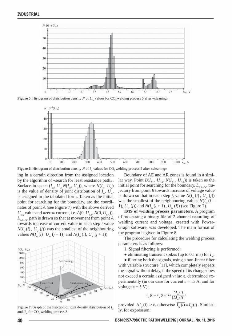
40 ISSN 0957-798X THE PATON WELDING JOURNAL, No. 11, 2016
INDUSTRIAL
ing in a certain direction from the assigned location by the algorithm of «search for least resistance path». Surface in space (Iw, Uw, N(Iw, Uw)), where N(Iw, Uw) is the value of density of joint distribution of Iw, Uw, is assigned in the tabulated form. Taken as the initial point for searching for the boundary, are the coordi-nates of point A (see Figure 7) with the above derived USA value and «zero» current, i.e. A(0, USA, N(0, USA)). LAR–SC path is drawn so that at movement from point A towards increase of current value in each step i value N(Iw (i) , Uw (j)) was the smallest of the neighbouring values N(Iw (i) , Uw (j – 1)) and N(Iw (i), Uw (j + 1)).
Boundary of AE and AR zones is found in a simi-lar way. Point B(IAE, USA, N(IAE, USA)) is taken as the initial point for searching for the boundary. LAR–OC tra-jectory from point B towards increase of voltage value is drawn so that in each step j, value N(Iw (i) , Uw (j)) was the smallest of the neighbouring values N(Iw (i – 1), Uw (j)) and N(Iw (i + 1) , Uw (j)) (see Figure 7).
IMS of welding process parameters. A program of processing a binary file of 2-channel recording of welding current and voltage, created with Power-Graph software, was developed. The main format of the program is given in Figure 8.
The procedure for calculating the welding process parameters is as follows:
1. Signal filtering is performed:● eliminating transient spikes (up to 0.1 ms) for Iw;● filtering both the signals, using a non-linear filter
with variable structure [11], which completely repeats the signal without delay, if the speed of its change does not exceed a certain assigned value ε, determined ex-perimentally (in our case for current ε = 15 A, and for voltage ε = 5 V);
( )( ) ( 1) | ( ) |
ww w
w
I iI i I i I i
D= − + e
D
provided |ΔIw (i)| > ε, otherwise ( ) ( )w w
I i I i= . Similar-ly, for expression:
Figure 5. Histogram of distribution density N of Uw values for CO2 welding process 5 after «cleaning»
Figure 6. Histogram of distribution density N of Iw values for CO2 welding process 5 after «cleaning»
Figure 7. Graph of the function of joint density distribution of Iw and Uw for CO2 welding process 3
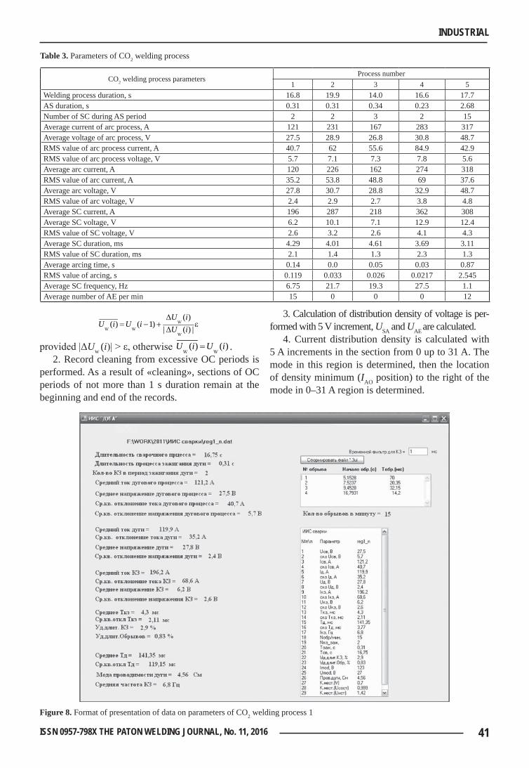
41ISSN 0957-798X THE PATON WELDING JOURNAL, No. 11, 2016
INDUSTRIAL
( )( ) ( 1) | ( ) |
ww w
w
U iU i U i U i
D= − + e
D
provided |ΔUw (i)| > ε, otherwise ( ) ( )w w
U i U i= .2. Record cleaning from excessive OC periods is
performed. As a result of «cleaning», sections of OC periods of not more than 1 s duration remain at the beginning and end of the records.
3. Calculation of distribution density of voltage is per-formed with 5 V increment, USA and UAE are calculated.
4. Current distribution density is calculated with 5 A increments in the section from 0 up to 31 A. The mode in this region is determined, then the location of density minimum (IAO position) to the right of the mode in 0–31 A region is determined.
Table 3. Parameters of CO2 welding process
CO2 welding process parametersProcess number
1 2 3 4 5Welding process duration, s 16.8 19.9 14.0 16.6 17.7AS duration, s 0.31 0.31 0.34 0.23 2.68Number of SC during AS period 2 2 3 2 15Average current of arc process, A 121 231 167 283 317Average voltage of arc process, V 27.5 28.9 26.8 30.8 48.7RMS value of arc process current, A 40.7 62 55.6 84.9 42.9RMS value of arc process voltage, V 5.7 7.1 7.3 7.8 5.6Average arc current, A 120 226 162 274 318RMS value of arc current, A 35.2 53.8 48.8 69 37.6Average arc voltage, V 27.8 30.7 28.8 32.9 48.7RMS value of arc voltage, V 2.4 2.9 2.7 3.8 4.8Average SC current, A 196 287 218 362 308Average SC voltage, V 6.2 10.1 7.1 12.9 12.4RMS value of SC voltage, V 2.6 3.2 2.6 4.1 4.3Average SC duration, ms 4.29 4.01 4.61 3.69 3.11RMS value of SC duration, ms 2.1 1.4 1.3 2.3 1.3Average arcing time, s 0.14 0.0 0.05 0.03 0.87RMS value of arcing, s 0.119 0.033 0.026 0.0217 2.545Average SC frequency, Hz 6.75 21.7 19.3 27.5 1.1Average number of AE per min 15 0 0 0 12
Figure 8. Format of presentation of data on parameters of CO2 welding process 1
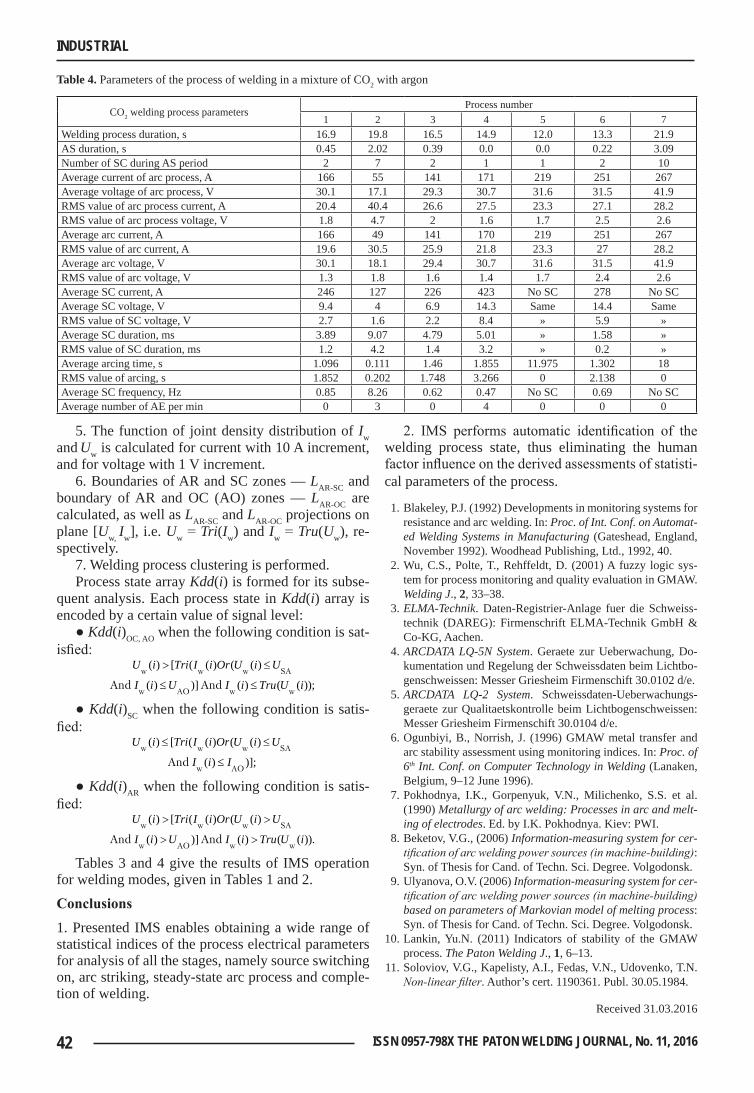
42 ISSN 0957-798X THE PATON WELDING JOURNAL, No. 11, 2016
INDUSTRIAL
5. The function of joint density distribution of Iw and Uw is calculated for current with 10 A increment, and for voltage with 1 V increment.
6. Boundaries of AR and SC zones — LAR-SC and boundary of AR and OC (AO) zones — LAR-OC are calculated, as well as LAR-SC and LAR-OC projections on plane [Uw, Iw], i.e. Uw = Tri(Iw) and Iw = Tru(Uw), re-spectively.
7. Welding process clustering is performed.Process state array Kdd(i) is formed for its subse-
quent analysis. Each process state in Kdd(i) array is encoded by a certain value of signal level:
● Kdd(i)OC, AO when the following condition is sat-isfied:
( ) [ ( ( ) ( ( )
( ) )] ( ) ( ( ));w w w SA
w AO w wAnd And
U i Tri I i Or U i U
I i U I i Tru U i
> ≤
≤ ≤
● Kdd(i)SC when the following condition is satis-fied:
( ) [ ( ( ) ( ( )
( ) )];w w w SA
w AOAnd
U i Tri I i Or U i U
I i I
≤ ≤
≤
● Kdd(i)AR when the following condition is satis-fied:
( ) [ ( ( ) ( ( )
( ) )] ( ) ( ( )).w w w SA
w AO w wAnd And
U i Tri I i Or U i U
I i U I i Tru U i
> >
> >
Tables 3 and 4 give the results of IMS operation for welding modes, given in Tables 1 and 2.
Conclusions1. Presented IMS enables obtaining a wide range of statistical indices of the process electrical parameters for analysis of all the stages, namely source switching on, arc striking, steady-state arc process and comple-tion of welding.
2. IMS performs automatic identification of the welding process state, thus eliminating the human factor influence on the derived assessments of statisti-cal parameters of the process.
1. Blakeley, P.J. (1992) Developments in monitoring systems for resistance and arc welding. In: Proc. of Int. Conf. on Automat-ed Welding Systems in Manufacturing (Gateshead, England, November 1992). Woodhead Publishing, Ltd., 1992, 40.
2. Wu, C.S., Polte, T., Rehffeldt, D. (2001) A fuzzy logic sys-tem for process monitoring and quality evaluation in GMAW. Welding J., 2, 33–38.
3. ELMA-Technik. Daten-Registrier-Anlage fuer die Schweiss-technik (DAREG): Firmenschrift ELMA-Technik GmbH & Co-KG, Aachen.
4. ARCDATA LQ-5N System. Geraete zur Ueberwachung, Do-kumentation und Regelung der Schweissdaten beim Lichtbo-genschweissen: Messer Griesheim Firmenschift 30.0102 d/e.
5. ARCDATA LQ-2 System. Schweissdaten-Ueberwachungs-geraete zur Qualitaetskontrolle beim Lichtbogenschweissen: Messer Griesheim Firmenschift 30.0104 d/e.
6. Ogunbiyi, B., Norrish, J. (1996) GMAW metal transfer and arc stability assessment using monitoring indices. In: Proc. of 6th Int. Conf. on Computer Technology in Welding (Lanaken, Belgium, 9–12 June 1996).
7. Pokhodnya, I.K., Gorpenyuk, V.N., Milichenko, S.S. et al. (1990) Metallurgy of arc welding: Processes in arc and melt-ing of electrodes. Ed. by I.K. Pokhodnya. Kiev: PWI.
8. Beketov, V.G., (2006) Information-measuring system for cer-tification of arc welding power sources (in machine-building): Syn. of Thesis for Cand. of Techn. Sci. Degree. Volgodonsk.
9. Ulyanova, O.V. (2006) Information-measuring system for cer-tification of arc welding power sources (in machine-building) based on parameters of Markovian model of melting process: Syn. of Thesis for Cand. of Techn. Sci. Degree. Volgodonsk.
10. Lankin, Yu.N. (2011) Indicators of stability of the GMAW process. The Paton Welding J., 1, 6–13.
11. Soloviov, V.G., Kapelisty, A.I., Fedas, V.N., Udovenko, T.N. Non-linear filter. Author’s cert. 1190361. Publ. 30.05.1984.
Received 31.03.2016
Table 4. Parameters of the process of welding in a mixture of CO2 with argon
CO2 welding process parametersProcess number
1 2 3 4 5 6 7Welding process duration, s 16.9 19.8 16.5 14.9 12.0 13.3 21.9AS duration, s 0.45 2.02 0.39 0.0 0.0 0.22 3.09Number of SC during AS period 2 7 2 1 1 2 10Average current of arc process, A 166 55 141 171 219 251 267Average voltage of arc process, V 30.1 17.1 29.3 30.7 31.6 31.5 41.9RMS value of arc process current, A 20.4 40.4 26.6 27.5 23.3 27.1 28.2RMS value of arc process voltage, V 1.8 4.7 2 1.6 1.7 2.5 2.6Average arc current, A 166 49 141 170 219 251 267RMS value of arc current, A 19.6 30.5 25.9 21.8 23.3 27 28.2Average arc voltage, V 30.1 18.1 29.4 30.7 31.6 31.5 41.9RMS value of arc voltage, V 1.3 1.8 1.6 1.4 1.7 2.4 2.6Average SC current, A 246 127 226 423 No SC 278 No SCAverage SC voltage, V 9.4 4 6.9 14.3 Same 14.4 SameRMS value of SC voltage, V 2.7 1.6 2.2 8.4 » 5.9 »Average SC duration, ms 3.89 9.07 4.79 5.01 » 1.58 »RMS value of SC duration, ms 1.2 4.2 1.4 3.2 » 0.2 »Average arcing time, s 1.096 0.111 1.46 1.855 11.975 1.302 18RMS value of arcing, s 1.852 0.202 1.748 3.266 0 2.138 0Average SC frequency, Hz 0.85 8.26 0.62 0.47 No SC 0.69 No SCAverage number of AE per min 0 3 0 4 0 0 0
43ISSN 0957-798X THE PATON WELDING JOURNAL, No. 11, 2016
INDUSTRIAL
doi.org/10.15407/tpwj2016.11.07
DEVICE FOR EXCITATION AND STABILIZATION OF WELDING ARC
V.V. BURLAKA and S.V. GULAKOVState Higher Educational Establishment «Pre-Azov State Technical University» (PSTU)
7 Universitetskaya Str., 87500, Mariupol, Ukraine. Е-mail: offiсе@рstu.edu
The circuit design of the device for formation of increased voltage was proposed, providing facilitation of ignition and stabilization of welding arc burning at direct/alternating current. The device operates according to the algorithm Lift-Arc and provides ignition of the arc at a minimum required power due to limitation of rate of voltage growth at the arc gap. For safe operation the time limit for action of higher voltage was also introduced. Due to application of the ad-vanced elementary base it was possible to simplify the electric circuit of the device for arc stabilization at maintaining the high consumer properties. 10 Ref., 5 Figures.
K e y w o r d s : electric arc, welding, arc ignition, stabilization of arc burning, welding inverter, open-circuit voltage
In manual arc welding with a covered electrode, as well as in welding in inert gas (MIG), including that with a non-consumable electrode (TIG) the need is occurred, firstly, to facilitate the initiation of arc dis-charge, secondly, to stabilize the process of arc burn-ing. At the power supply from the alternating current mains, the repeated excitation of arc should occur af-ter each transition of power source voltage through zero. Moreover, in TIG welding it is desirable to lim-it the power, which is released at the arc gap break-down, as at the increased discharge power the erosion of non-consumable electrode occurs, which reduces its service life. Therefore, the urgent problem is the design of device for arc stabilization, which will re-alize the exciting of arc at the minimum required dis-charge energy and provide a stable burning of the arc during welding process.
In manual arc welding using electrodes at direct current with the power supply from inverter source the problems with ignition and maintaining of the arc (arc burns unstable, electrode often «sticks») are occurred. The cause is the low open-circuit voltage Uo-c of invert-er power sources for arc welding. Thus, for the sources, designed according to the bridge circuit, Uo-c amounts to 60–65 V; for the sources based on forward converter Uo-c amounts to 50–60 V (pulses of the amplitude of about 100 V and pulse duty factor of 0.5).
The conventional devices for arc stabilization in-clude step-up transformer, spark generator with a dis-charger and high-frequency (broadband) transformer, the secondary winding of which is connected in series or in parallel with the arc gap [1–4]. Such a circuit
allows forming high-voltage pulses at the arc gap and providing ignition of the arc. Among its disadvantag-es the large dimensions and weight of the transform-ers, complicated control of pulses power, wide range of generated electromagnetic interferences, short ser-vice life of discharger and the need in its periodical replacement should be mentioned.
In the works [5–8] the devices for arc stabilization are described, in which contact-free switching ele-ments like transistors and thyristors are applied. This provides a significant improvement in the reliability of welding equipment, fitted with such devices, and the possibility to control characteristics of igniting pulses within the wide ranges.
In the work [9] the device for arc stabilization was proposed, providing the control of power for exci-tation of the arc due to changes in the supply voltage of resonance circuits. In the circuit of the device the additional controllable source of the higher voltage of direct current, two resonant circuits with appropriate control circuits were introduced. This leads to compli-cation of circuit, increase in power losses and deterio-rates the consumer qualities of the device.
In the work [10] the method for increasing intensi-ty of plasma formation was proposed due to the use of several resonance circuits, operating at a phase shift and loaded to the common high-frequency transform-er. However, the use of non-firing thyristors in the de-vices as the key elements, does not allow increasing the operating frequency, simplifying the circuit and improving the weight and size characteristics of the arc stabilizer [9, 10].
© V.V. BURLAKA and S.V. GULAKOV, 2016
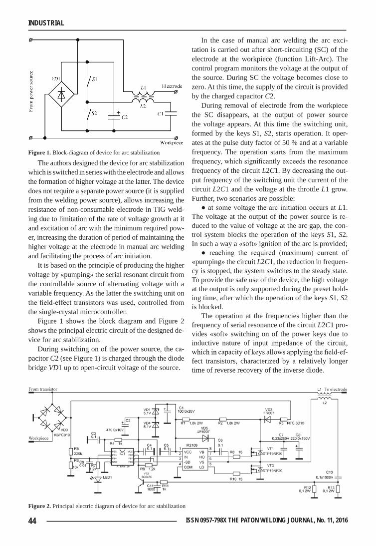
44 ISSN 0957-798X THE PATON WELDING JOURNAL, No. 11, 2016
INDUSTRIAL
The authors designed the device for arc stabilization which is switched in series with the electrode and allows the formation of higher voltage at the latter. The device does not require a separate power source (it is supplied from the welding power source), allows increasing the resistance of non-consumable electrode in TIG weld-ing due to limitation of the rate of voltage growth at it and excitation of arc with the minimum required pow-er, increasing the duration of period of maintaining the higher voltage at the electrode in manual arc welding and facilitating the process of arc initiation.
It is based on the principle of producing the higher voltage by «pumping» the serial resonant circuit from the controllable source of alternating voltage with a variable frequency. As the latter the switching unit on the field-effect transistors was used, controlled from the single-crystal microcontroller.
Figure 1 shows the block diagram and Figure 2 shows the principal electric circuit of the designed de-vice for arc stabilization.
During switching on of the power source, the ca-pacitor C2 (see Figure 1) is charged through the diode bridge VD1 up to open-circuit voltage of the source.
In the case of manual arc welding the arc exci-tation is carried out after short-circuiting (SC) of the electrode at the workpiece (function Lift-Arc). The control program monitors the voltage at the output of the source. During SC the voltage becomes close to zero. At this time, the supply of the circuit is provided by the charged capacitor C2.
During removal of electrode from the workpiece the SC disappears, at the output of power source the voltage appears. At this time the switching unit, formed by the keys S1, S2, starts operation. It oper-ates at the pulse duty factor of 50 % and at a variable frequency. The operation starts from the maximum frequency, which significantly exceeds the resonance frequency of the circuit L2C1. By decreasing the out-put frequency of the switching unit the current of the circuit L2C1 and the voltage at the throttle L1 grow. Further, two scenarios are possible:
● at some voltage the arc initiation occurs at L1. The voltage at the output of the power source is re-duced to the value of voltage at the arc gap, the con-trol system blocks the operation of the keys S1, S2. In such a way a «soft» ignition of the arc is provided;
● reaching the required (maximum) current of «pumping» the circuit L2C1, the reduction in frequen-cy is stopped, the system switches to the steady state. To provide the safe use of the device, the high voltage at the output is only supported during the preset hold-ing time, after which the operation of the keys S1, S2 is blocked.
The operation at the frequencies higher than the frequency of serial resonance of the circuit L2C1 pro-vides «soft» switching on of the power keys due to inductive nature of input impedance of the circuit, which in capacity of keys allows applying the field-ef-fect transistors, characterized by a relatively longer time of reverse recovery of the inverse diode.
Figure 1. Block-diagram of device for arc stabilization
Figure 2. Principal electric diagram of device for arc stabilization
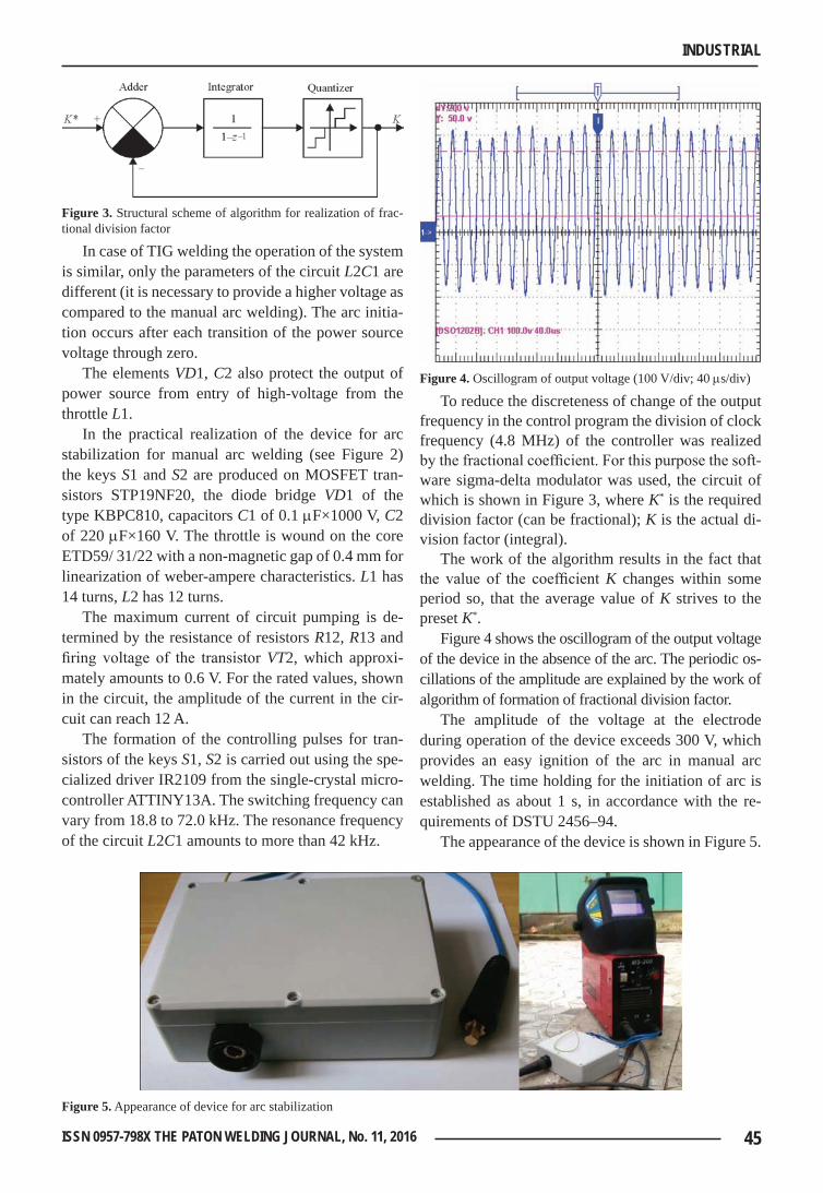
45ISSN 0957-798X THE PATON WELDING JOURNAL, No. 11, 2016
INDUSTRIAL
In case of TIG welding the operation of the system is similar, only the parameters of the circuit L2C1 are different (it is necessary to provide a higher voltage as compared to the manual arc welding). The arc initia-tion occurs after each transition of the power source voltage through zero.
The elements VD1, C2 also protect the output of power source from entry of high-voltage from the throttle L1.
In the practical realization of the device for arc stabilization for manual arc welding (see Figure 2) the keys S1 and S2 are produced on MOSFET tran-sistors STP19NF20, the diode bridge VD1 of the type KBPC810, capacitors C1 of 0.1 mF×1000 V, C2 of 220 mF×160 V. The throttle is wound on the core ETD59/ 31/22 with a non-magnetic gap of 0.4 mm for linearization of weber-ampere characteristics. L1 has 14 turns, L2 has 12 turns.
The maximum current of circuit pumping is de-termined by the resistance of resistors R12, R13 and firing voltage of the transistor VT2, which approxi-mately amounts to 0.6 V. For the rated values, shown in the circuit, the amplitude of the current in the cir-cuit can reach 12 A.
The formation of the controlling pulses for tran-sistors of the keys S1, S2 is carried out using the spe-cialized driver IR2109 from the single-crystal micro-controller ATTINY13A. The switching frequency can vary from 18.8 to 72.0 kHz. The resonance frequency of the circuit L2C1 amounts to more than 42 kHz.
To reduce the discreteness of change of the output frequency in the control program the division of clock frequency (4.8 MHz) of the controller was realized by the fractional coefficient. For this purpose the soft-ware sigma-delta modulator was used, the circuit of which is shown in Figure 3, where K* is the required division factor (can be fractional); K is the actual di-vision factor (integral).
The work of the algorithm results in the fact that the value of the coefficient K changes within some period so, that the average value of K strives to the preset K*.
Figure 4 shows the oscillogram of the output voltage of the device in the absence of the arc. The periodic os-cillations of the amplitude are explained by the work of algorithm of formation of fractional division factor.
The amplitude of the voltage at the electrode during operation of the device exceeds 300 V, which provides an easy ignition of the arc in manual arc welding. The time holding for the initiation of arc is established as about 1 s, in accordance with the re-quirements of DSTU 2456–94.
The appearance of the device is shown in Figure 5.
Figure 3. Structural scheme of algorithm for realization of frac-tional division factor
Figure 4. Oscillogram of output voltage (100 V/div; 40 ms/div)
Figure 5. Appearance of device for arc stabilization
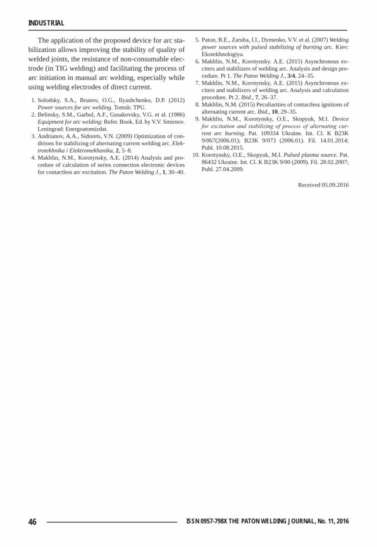
46 ISSN 0957-798X THE PATON WELDING JOURNAL, No. 11, 2016
INDUSTRIAL
The application of the proposed device for arc sta-bilization allows improving the stability of quality of welded joints, the resistance of non-consumable elec-trode (in TIG welding) and facilitating the process of arc initiation in manual arc welding, especially while using welding electrodes of direct current.
1. Solodsky, S.A., Brunov, O.G., Ilyashchenko, D.P. (2012) Power sources for arc welding. Tomsk: TPU.
2. Belinsky, S.M., Garbul, A.F., Gusakovsky, V.G. et al. (1986) Equipment for arc welding: Refer. Book. Ed. by V.V. Smirnov. Leningrad: Energoatomizdat.
3. Andrianov, A.A., Sidorets, V.N. (2009) Optimization of con-ditions for stabilizing of alternating current welding arc. Elek-trotekhnika i Elektromekhanika, 2, 5–8.
4. Makhlin, N.M., Korotynsky, A.E. (2014) Analysis and pro-cedure of calculation of series connection electronic devices for contactless arc excitation. The Paton Welding J., 1, 30–40.
5. Paton, B.E., Zaruba, I.I., Dymenko, V.V. et al. (2007) Welding power sources with pulsed stabilizing of burning arc. Kiev: Ekotekhnologiya.
6. Makhlin, N.M., Korotynsky. A.E. (2015) Asynchronous ex-citers and stabilizers of welding arc. Analysis and design pro-cedure. Pt 1. The Paton Welding J., 3/4, 24–35.
7. Makhlin, N.M., Korotynsky, A.E. (2015) Asynchronous ex-citers and stabilizers of welding arc. Analysis and calculation procedure. Pt 2. Ibid., 7, 26–37.
8. Makhlin, N.M. (2015) Peculiarities of contactless ignitions of alternating current arc. Ibid., 10, 29–35.
9. Makhlin, N.M., Korotynsky, O.E., Skopyuk, M.I. Device for excitation and stabilizing of process of alternating cur-rent arc burning. Pat. 109334 Ukraine. Int. Cl. K B23K 9/067(2006.01); B23K 9/073 (2006.01). Fil. 14.01.2014; Publ. 10.08.2015.
10. Korotynsky, O.E., Skopyuk, M.I. Pulsed plasma source. Pat. 86432 Ukraine. Int. Cl. K B23K 9/00 (2009). Fil. 28.02.2007; Publ. 27.04.2009.
Received 05.09.2016