NON-CATALOG Digital Step Attenuator - Mini Circuits · The DAT-15575-SP is a 75Ω RF digital step...
12
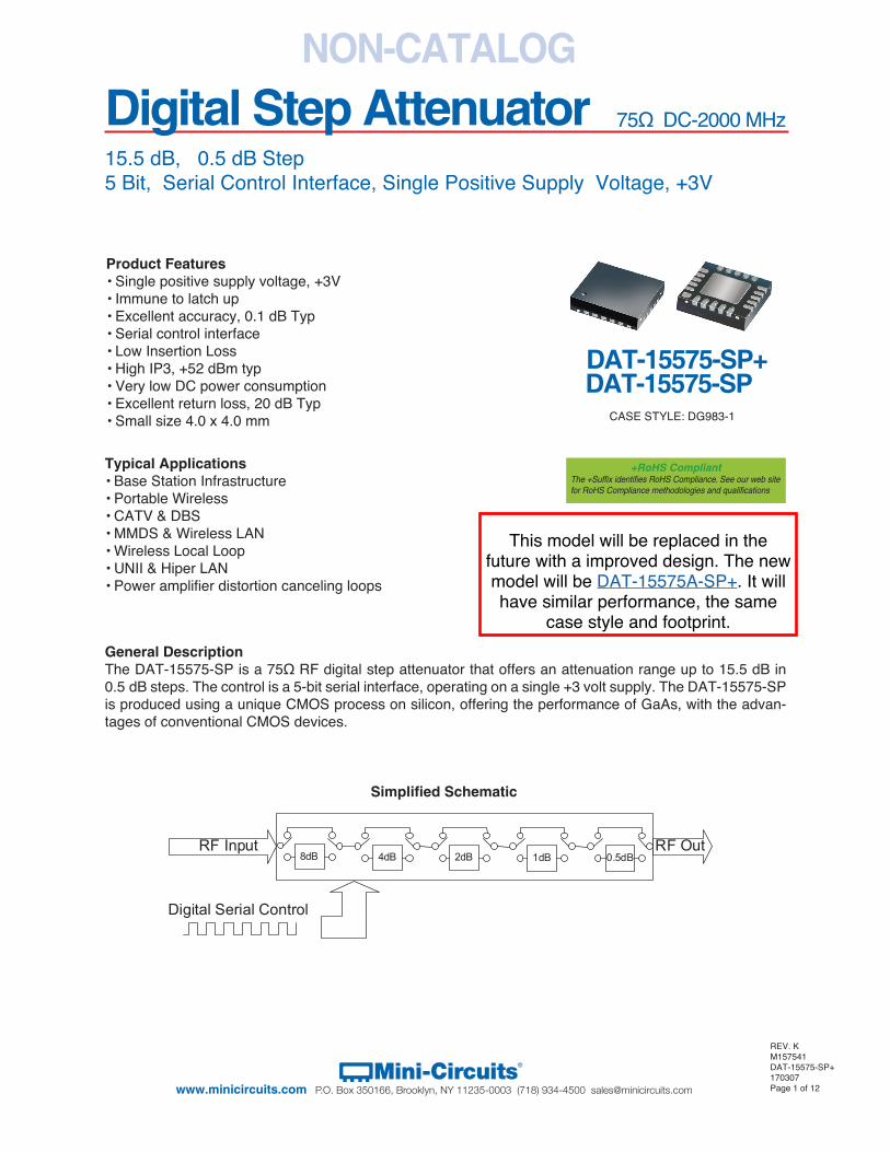
REV. K M157541 DAT-15575-SP+ 170307 Page 1 of 12 Mini-Circuits ® www.minicircuits.com P.O. Box 350166, Brooklyn, NY 11235-0003 (718) 934-4500 [email protected] NON-CATALOG Product Features • Single positive supply voltage, +3V • Immune to latch up • Excellent accuracy, 0.1 dB Typ • Serial control interface • Low Insertion Loss • High IP3, +52 dBm typ • Very low DC power consumption • Excellent return loss, 20 dB Typ • Small size 4.0 x 4.0 mm Typical Applications • Base Station Infrastructure • Portable Wireless • CATV & DBS • MMDS & Wireless LAN • Wireless Local Loop • UNII & Hiper LAN • Power amplifier distortion canceling loops General Description The DAT-15575-SP is a 75Ω RF digital step attenuator that offers an attenuation range up to 15.5 dB in 0.5 dB steps. The control is a 5-bit serial interface, operating on a single +3 volt supply. The DAT-15575-SP is produced using a unique CMOS process on silicon, offering the performance of GaAs, with the advan- tages of conventional CMOS devices. Digital Step Attenuator 15.5 dB, 0.5 dB Step 5 Bit, Serial Control Interface, Single Positive Supply Voltage, +3V 75Ω DC-2000 MHz Simplified Schematic Digital Serial Control RF Input 8dB 4dB 2dB 1dB 0.5dB RF Out DAT-15575-SP+ DAT-15575-SP CASE STYLE: DG983-1 +RoHS Compliant The +Suffix identifies RoHS Compliance. See our web site for RoHS Compliance methodologies and qualifications This model will be replaced in the future with a improved design. The new model will be DAT-15575A-SP+. It will have similar performance, the same case style and footprint.
Transcript of NON-CATALOG Digital Step Attenuator - Mini Circuits · The DAT-15575-SP is a 75Ω RF digital step...
REV. KM157541 DAT-15575-SP+170307Page 1 of 12
Mini-Circuits®
www.minicircuits.com P.O. Box 350166, Brooklyn, NY 11235-0003 (718) 934-4500 [email protected]
NON-CATALOG
Product Features• Single positive supply voltage, +3V• Immune to latch up• Excellent accuracy, 0.1 dB Typ• Serial control interface• Low Insertion Loss• High IP3, +52 dBm typ• Very low DC power consumption• Excellent return loss, 20 dB Typ• Small size 4.0 x 4.0 mm
Typical Applications• Base Station Infrastructure• Portable Wireless• CATV & DBS• MMDS & Wireless LAN• Wireless Local Loop• UNII & Hiper LAN• Power amplifier distortion canceling loops
General DescriptionThe DAT-15575-SP is a 75Ω RF digital step attenuator that offers an attenuation range up to 15.5 dB in 0.5 dB steps. The control is a 5-bit serial interface, operating on a single +3 volt supply. The DAT-15575-SP is produced using a unique CMOS process on silicon, offering the performance of GaAs, with the advan-tages of conventional CMOS devices.
Digital Step Attenuator 15.5 dB, 0.5 dB Step5 Bit, Serial Control Interface, Single Positive Supply Voltage, +3V
75Ω DC-2000 MHz
Simplified Schematic
Digital Serial Control
RF Input8dB 4dB 2dB 1dB 0.5dB
RF Out
DAT-15575-SP+DAT-15575-SP
CASE STYLE: DG983-1
+RoHS CompliantThe +Suffix identifies RoHS Compliance. See our web site for RoHS Compliance methodologies and qualifications
This model will be replaced in thefuture with a improved design. The newmodel will be DAT-15575A-SP+. It willhave similar performance, the same
case style and footprint.
Digital Step Attenuator
Page 2 of 12
DAT-15575-SPDAT-15575-SP+
Mini-Circuits®
www.minicircuits.com P.O. Box 350166, Brooklyn, NY 11235-0003 (718) 934-4500 [email protected]
NON-CATALOG
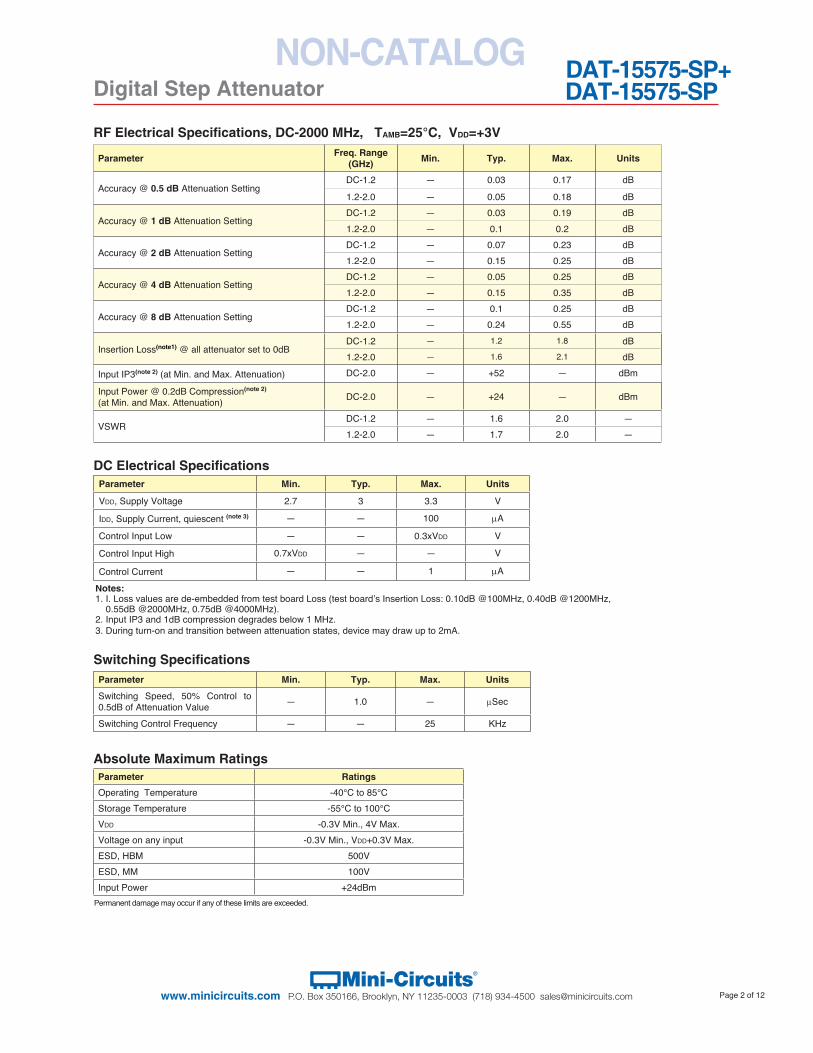
RF Electrical Specifications, DC-2000 MHz, TAMB=25°C, VDD=+3V
Absolute Maximum Ratings
Parameter Freq. Range(GHz) Min. Typ. Max. Units
Accuracy @ 0.5 dB Attenuation SettingDC-1.2 — 0.03 0.17 dB
1.2-2.0 — 0.05 0.18 dB
Accuracy @ 1 dB Attenuation SettingDC-1.2 — 0.03 0.19 dB
1.2-2.0 — 0.1 0.2 dB
Accuracy @ 2 dB Attenuation SettingDC-1.2 — 0.07 0.23 dB
1.2-2.0 — 0.15 0.25 dB
Accuracy @ 4 dB Attenuation SettingDC-1.2 — 0.05 0.25 dB
1.2-2.0 — 0.15 0.35 dB
Accuracy @ 8 dB Attenuation SettingDC-1.2 — 0.1 0.25 dB
1.2-2.0 — 0.24 0.55 dB
Insertion Loss(note1) @ all attenuator set to 0dBDC-1.2 — 1.2 1.8 dB
1.2-2.0 — 1.6 2.1 dB
Input IP3(note 2) (at Min. and Max. Attenuation) DC-2.0 — +52 — dBm
Input Power @ 0.2dB Compression(note 2) (at Min. and Max. Attenuation)
DC-2.0 — +24 — dBm
VSWRDC-1.2 — 1.6 2.0 —
1.2-2.0 — 1.7 2.0 —
Parameter Ratings
Operating Temperature -40°C to 85°C
Storage Temperature -55°C to 100°C
Vdd -0.3V Min., 4V Max.
Voltage on any input -0.3V Min., Vdd+0.3V Max.
ESD, HBM 500V
ESD, MM 100V
Input Power +24dBm
Parameter Min. Typ. Max. Units
Vdd, Supply Voltage 2.7 3 3.3 V
Idd, Supply Current, quiescent (note 3) — — 100 mA
Control Input Low — — 0.3xVdd V
Control Input High 0.7xVdd — — V
Control Current — — 1 mA
DC Electrical Specifications
Parameter Min. Typ. Max. Units
Switching Speed, 50% Control to 0.5dB of Attenuation Value — 1.0 — mSec
Switching Control Frequency — — 25 KHz
Switching Specifications
Permanent damage may occur if any of these limits are exceeded.
Notes:1. I. Loss values are de-embedded from test board Loss (test board’s Insertion Loss: 0.10dB @100MHz, 0.40dB @1200MHz, 0.55dB @2000MHz, 0.75dB @4000MHz).2. Input IP3 and 1dB compression degrades below 1 MHz.3. During turn-on and transition between attenuation states, device may draw up to 2mA.
Digital Step Attenuator
Page 3 of 12
DAT-15575-SPDAT-15575-SP+
Mini-Circuits®
www.minicircuits.com P.O. Box 350166, Brooklyn, NY 11235-0003 (718) 934-4500 [email protected]
NON-CATALOG
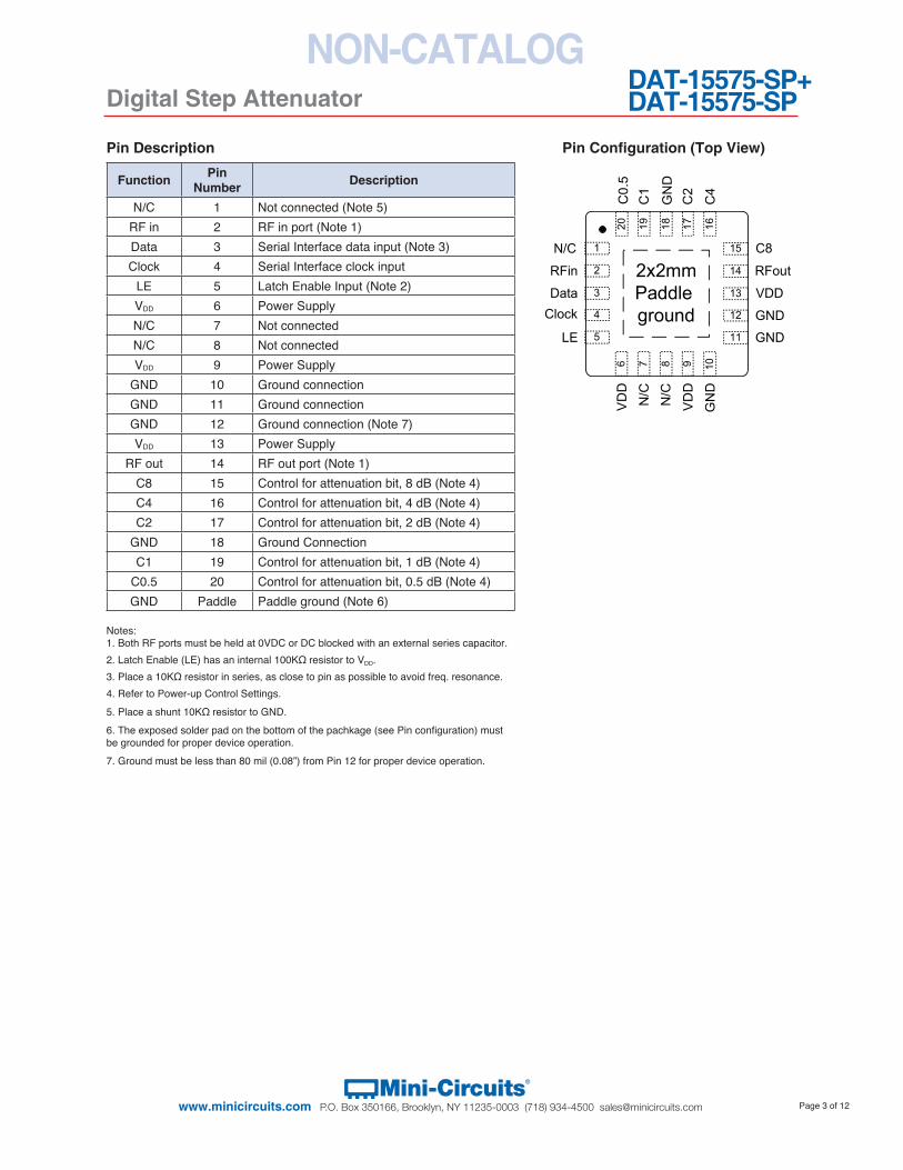
Function Pin Number Description
N/C 1 Not connected (Note 5)
RF in 2 RF in port (Note 1)
Data 3 Serial Interface data input (Note 3)
Clock 4 Serial Interface clock input
LE 5 Latch Enable Input (Note 2)
VDD 6 Power Supply
N/C 7 Not connected
N/C 8 Not connected
VDD 9 Power Supply
GND 10 Ground connection
GND 11 Ground connection
GND 12 Ground connection (Note 7)
VDD 13 Power Supply
RF out 14 RF out port (Note 1)
C8 15 Control for attenuation bit, 8 dB (Note 4)
C4 16 Control for attenuation bit, 4 dB (Note 4)
C2 17 Control for attenuation bit, 2 dB (Note 4)
GND 18 Ground Connection
C1 19 Control for attenuation bit, 1 dB (Note 4)
C0.5 20 Control for attenuation bit, 0.5 dB (Note 4)
GND Paddle Paddle ground (Note 6)
Notes:1. Both RF ports must be held at 0VDC or DC blocked with an external series capacitor.
2. Latch Enable (LE) has an internal 100KΩ resistor to VDD.
3. Place a 10KΩ resistor in series, as close to pin as possible to avoid freq. resonance.
4. Refer to Power-up Control Settings.
5. Place a shunt 10KΩ resistor to GND.
6. The exposed solder pad on the bottom of the pachkage (see Pin configuration) must be grounded for proper device operation.
7. Ground must be less than 80 mil (0.08”) from Pin 12 for proper device operation.
Pin Description
Parallel
Serial
GNDGND
GN
D
GN
D
VDD
VD
D
VD
D
N/C
N/C
RFout
C8
LE
ClockData
RFin
N/C
C4
C2
C1
C0.
5
2x2mmPaddleground
15
14
13
12
11
1
2
3
4
5
6 7 8 9
20 19 18 17 1610
GNDGND
GN
D
GN
DGND
VD
D
VD
D
PU
P2
N/C
RFoutC8
LEGND
N/CRFin
N/C
C4
C2
C1
C0.
5
2x2mmPaddleground
15
14
13
12
11
1
2
3
4
5
6 7 8 9 10
20 19 18 17 16
Pin Configuration (Top View)
Digital Step Attenuator
Page 4 of 12
DAT-15575-SPDAT-15575-SP+
Mini-Circuits®
www.minicircuits.com P.O. Box 350166, Brooklyn, NY 11235-0003 (718) 934-4500 [email protected]
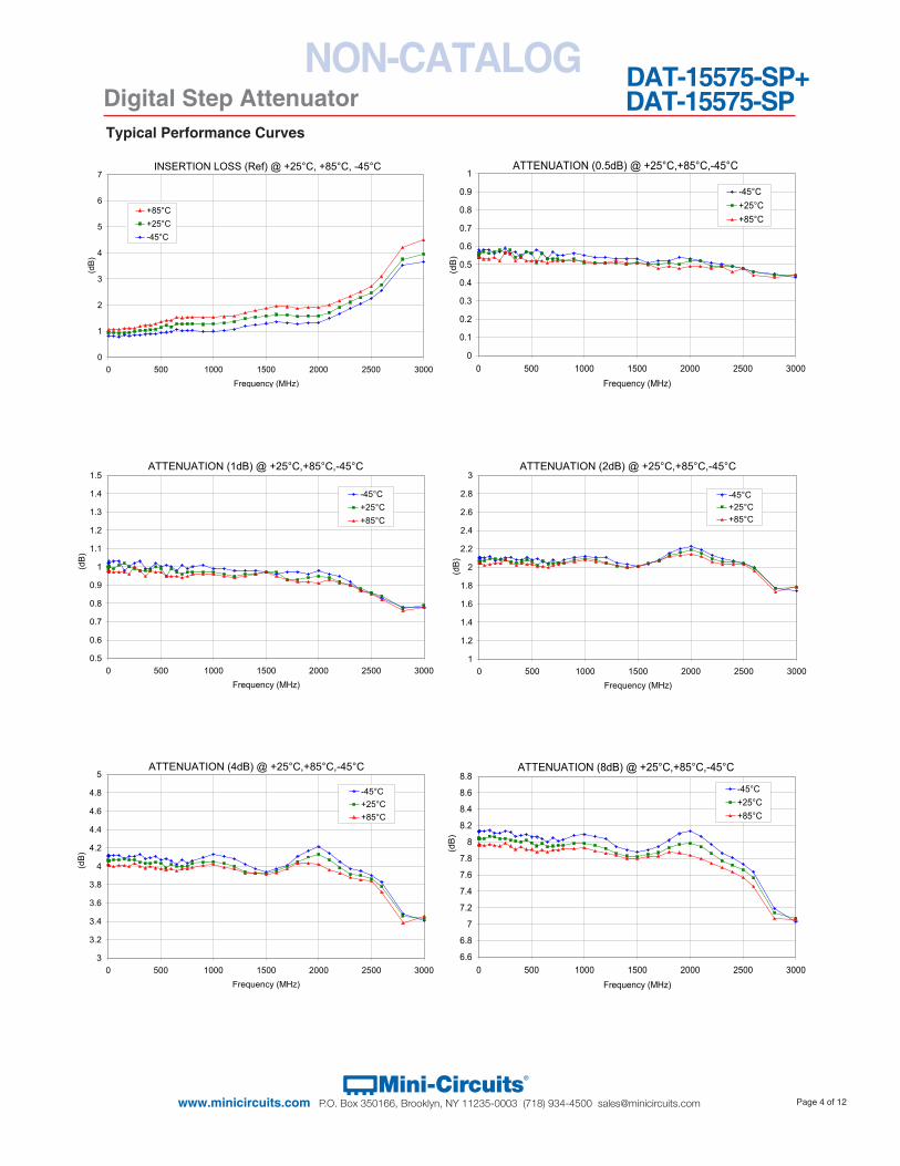
NON-CATALOGTypical Performance Curves
INSERTION LOSS (Ref) @ +25°C, +85°C, -45°C
0
1
2
3
4
5
6
7
0 500 1000 1500 2000 2500 3000Frequency (MHz)
(dB
)
+85°C+25°C-45°C
ATTENUATION (0.5dB) @ +25°C,+85°C,-45°C
0
0.1
0.2
0.3
0.4
0.5
0.6
0.7
0.8
0.9
1
0 500 1000 1500 2000 2500 3000Frequency (MHz)
(dB
)
-45°C+25°C+85°C
ATTENUATION (1dB) @ +25°C,+85°C,-45°C
0.5
0.6
0.7
0.8
0.9
1
1.1
1.2
1.3
1.4
1.5
0 500 1000 1500 2000 2500 3000Frequency (MHz)
(dB
)
-45°C+25°C+85°C
ATTENUATION (2dB) @ +25°C,+85°C,-45°C
1
1.2
1.4
1.6
1.8
2
2.2
2.4
2.6
2.8
3
0 500 1000 1500 2000 2500 3000Frequency (MHz)
(dB)
-45°C+25°C+85°C
ATTENUATION (4dB) @ +25°C,+85°C,-45°C
3
3.2
3.4
3.6
3.8
4
4.2
4.4
4.6
4.8
5
0 500 1000 1500 2000 2500 3000Frequency (MHz)
(dB)
-45°C+25°C+85°C
ATTENUATION (8dB) @ +25°C,+85°C,-45°C
6.6
6.8
7
7.2
7.4
7.6
7.8
8
8.2
8.4
8.6
8.8
0 500 1000 1500 2000 2500 3000Frequency (MHz)
(dB
)
-45°C+25°C+85°C

Digital Step Attenuator
Page 5 of 12
DAT-15575-SPDAT-15575-SP+
Mini-Circuits®
www.minicircuits.com P.O. Box 350166, Brooklyn, NY 11235-0003 (718) 934-4500 [email protected]
NON-CATALOGTypical Performance Curves
ATTENUATION (15.5dB) @ +25°C,+85°C,-45°C
12
13
14
15
16
17
18
0 500 1000 1500 2000 2500 3000Frequency (MHz)
(dB
)
-45°C+25°C+85°C
RETURN LOSS IN S11 (Ref) @ +25°C,+85°C,-45°C
0
10
20
30
40
50
0 500 1000 1500 2000 2500 3000Frequency (MHz)
(dB
)
-45°C+25°C+85°C
RETURN LOSS OUT S22 (Ref) @ +25°C,+85°C,-45°C
0
10
20
30
40
50
0 500 1000 1500 2000 2500 3000Frequency (MHz)
(dB
)
-45°C+25°C+85°C
RETURN LOSS IN S11 (Major Attenuation Steps) @ +25°C
0
10
20
30
40
50
0 500 1000 1500 2000 2500 3000Frequency (MHz)
(dB
)
ATT=0dB ATT=0.5dBATT=1dB ATT=2dBATT=4dB ATT=8dBATT=15.5dB
RETURN LOSS OUT S22 (Major Attenuation Steps) @ +25°C
0
10
20
30
40
50
0 500 1000 1500 2000 2500 3000Frequency (MHz)
(dB
)
ATT=0dB ATT=0.5dBATT=1dB ATT=2dBATT=4dB ATT=8dBATT=15.5dB
Digital Step Attenuator
Page 6 of 12
DAT-15575-SPDAT-15575-SP+
Mini-Circuits®
www.minicircuits.com P.O. Box 350166, Brooklyn, NY 11235-0003 (718) 934-4500 [email protected]
NON-CATALOGTypical Performance Curves
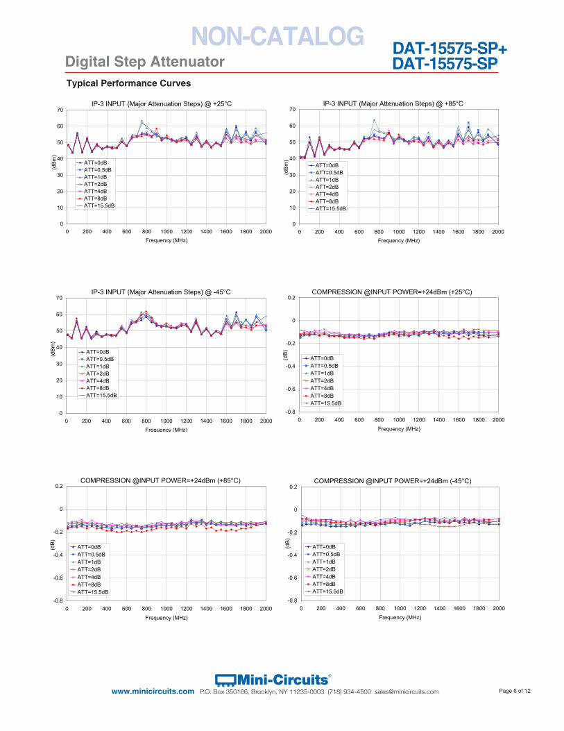
IP-3 INPUT (Major Attenuation Steps) @ +25°C
0
10
20
30
40
50
60
70
0 200 400 600 800 1000 1200 1400 1600 1800 2000Frequency (MHz)
(dB
m)
ATT=0dBATT=0.5dBATT=1dBATT=2dBATT=4dBATT=8dBATT=15.5dB
IP-3 INPUT (Major Attenuation Steps) @ +85°C
0
10
20
30
40
50
60
70
0 200 400 600 800 1000 1200 1400 1600 1800 2000Frequency (MHz)
(dB
m)
ATT=0dBATT=0.5dBATT=1dBATT=2dBATT=4dBATT=8dBATT=15.5dB
IP-3 INPUT (Major Attenuation Steps) @ -45°C
0
10
20
30
40
50
60
70
0 200 400 600 800 1000 1200 1400 1600 1800 2000Frequency (MHz)
(dB
m)
ATT=0dBATT=0.5dBATT=1dBATT=2dBATT=4dBATT=8dBATT=15.5dB
COMPRESSION @INPUT POWER=+24dBm (+25°C)
-0.8
-0.6
-0.4
-0.2
0
0.2
0 200 400 600 800 1000 1200 1400 1600 1800 2000Frequency (MHz)
(dB
)
ATT=0dBATT=0.5dBATT=1dBATT=2dBATT=4dBATT=8dBATT=15.5dB
COMPRESSION @INPUT POWER=+24dBm (+85°C)
-0.8
-0.6
-0.4
-0.2
0
0.2
0 200 400 600 800 1000 1200 1400 1600 1800 2000Frequency (MHz)
(dB
)
ATT=0dBATT=0.5dBATT=1dBATT=2dBATT=4dBATT=8dBATT=15.5dB
COMPRESSION @INPUT POWER=+24dBm (-45°C)
-0.8
-0.6
-0.4
-0.2
0
0.2
0 200 400 600 800 1000 1200 1400 1600 1800 2000Frequency (MHz)
(dB
)
ATT=0dBATT=0.5dBATT=1dBATT=2dBATT=4dBATT=8dBATT=15.5dB
Digital Step Attenuator
Page 7 of 12
DAT-15575-SPDAT-15575-SP+
Mini-Circuits®
www.minicircuits.com P.O. Box 350166, Brooklyn, NY 11235-0003 (718) 934-4500 [email protected]
NON-CATALOG
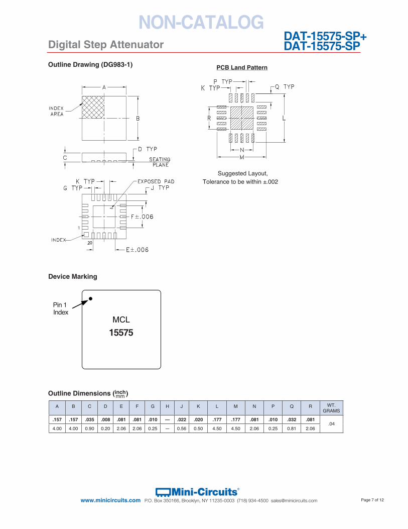
Outline Drawing (DG983-1)
Device Marking
Outline Dimensions ( )inchmm
A B C D E F G H J K L M N P Q R WT. GRAMS
.157 .157 .035 .008 .081 .081 .010 — .022 .020 .177 .177 .081 .010 .032 .081.04
4.00 4.00 0.90 0.20 2.06 2.06 0.25 — 0.56 0.50 4.50 4.50 2.06 0.25 0.81 2.06
Suggested Layout, Tolerance to be within ±.002
PCB Land Pattern
MCL
Pin 1 Index
15575
Digital Step Attenuator
Page 8 of 12
DAT-15575-SPDAT-15575-SP+
Mini-Circuits®
www.minicircuits.com P.O. Box 350166, Brooklyn, NY 11235-0003 (718) 934-4500 [email protected]
NON-CATALOG
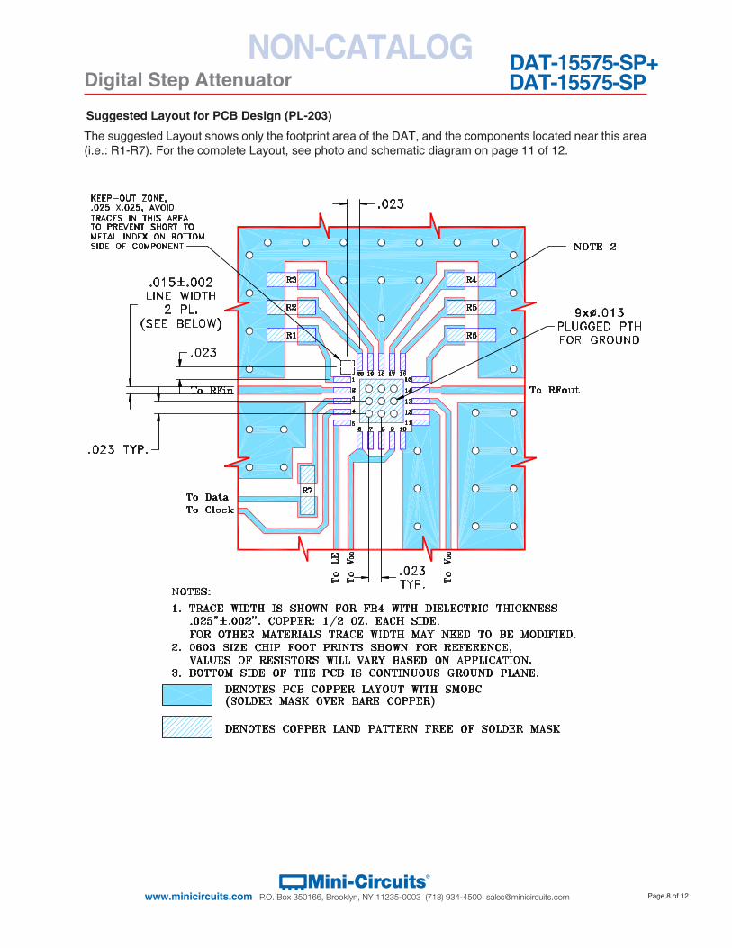
Suggested Layout for PCB Design (PL-203)
The suggested Layout shows only the footprint area of the DAT, and the components located near this area (i.e.: R1-R7). For the complete Layout, see photo and schematic diagram on page 11 of 12.
Digital Step Attenuator
Page 9 of 12
DAT-15575-SPDAT-15575-SP+
Mini-Circuits®
www.minicircuits.com P.O. Box 350166, Brooklyn, NY 11235-0003 (718) 934-4500 [email protected]
NON-CATALOG
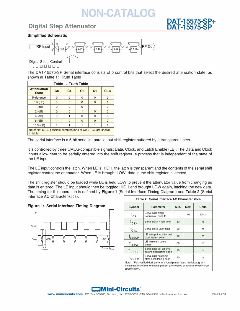
The serial interface is a 5-bit serial in, parallel-out shift register buffered by a transparent latch.
It is controlled by three CMOS-compatible signals: Data, Clock, and Latch Enable (LE). The Data and Clock inputs allow data to be serially entered into the shift register, a process that is independent of the state of the LE input.
The LE input controls the latch. When LE is HIGH, the latch is transparent and the contents of the serial shift register control the attenuator. When LE is brought LOW, data in the shift register is latched.
The shift register should be loaded while LE is held LOW to prevent the attenuator value from changing as data is entered. The LE input should then be toggled HIGH and brought LOW again, latching the new data. The timing for this operation is defined by Figure 1 (Serial Interface Timing Diagram) and Table 2 (Serial Interface AC Characteristics).
Simplified Schematic
Figure 1: Serial Interface Timing Diagram
Table 1. Truth TableAttenuation
State C8 C4 C2 C1 C0.5
Reference 0 0 0 0 0
0.5 (dB) 0 0 0 0 1
1 (dB) 0 0 0 1 0
2 (dB) 0 0 1 0 0
4 (dB) 0 1 0 0 0
8 (dB) 1 0 0 0 0
15.5 (dB) 1 1 1 1 1
Note: Not all 32 possible combinations of C0.5 - C8 are shown in table
Table 2. Serial Interface AC Characteristics
Symbol Parameter Min. Max. Units
fClkSerial data clockfrequency (Note 1) 10 MHz
tClkHSerial clock HIGH time 30 ns
tClkLSerial clock LOW time 30 ns
tLESUPLE set-up time after last clock falling edge 10 ns
tLEPWLE minimum pulse width 30 ns
tSDSUPSerial data set-up time before clock rising edge 10 ns
tSDHLDSerial data hold timeafter clock falling edge 10 ns
Note 1. Fclk verified during the functional pattern test. Serial program-ming sections of the functional pattern are clocked at 10MHz to verify Fclk specification.
The DAT-15575-SP Serial interface consists of 5 control bits that select the desired attenuation state, as shown in Table 1: Truth Table
Digital Serial Control
RF Input8dB 4dB 2dB 1dB 0.5dB
RF Out
LE
Clock
Data LSBMSB
tLESUP
tSDSUP
tLLEPW
tSDHLD
Digital Step Attenuator
Page 10 of 12
DAT-15575-SPDAT-15575-SP+
Mini-Circuits®
www.minicircuits.com P.O. Box 350166, Brooklyn, NY 11235-0003 (718) 934-4500 [email protected]
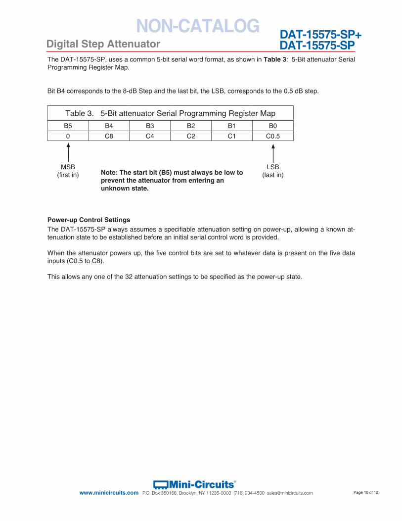
NON-CATALOGThe DAT-15575-SP, uses a common 5-bit serial word format, as shown in Table 3: 5-Bit attenuator Serial Programming Register Map.
Bit B4 corresponds to the 8-dB Step and the last bit, the LSB, corresponds to the 0.5 dB step.
The DAT-15575-SP always assumes a specifiable attenuation setting on power-up, allowing a known at-tenuation state to be established before an initial serial control word is provided.
When the attenuator powers up, the five control bits are set to whatever data is present on the five data inputs (C0.5 to C8).
This allows any one of the 32 attenuation settings to be specified as the power-up state.
Power-up Control Settings
Table 3. 5-Bit attenuator Serial Programming Register Map
B5 B4 B3 B2 B1 B0
0 C8 C4 C2 C1 C0.5
MSB(first in)
LSB(last in)Note: The start bit (B5) must always be low to
prevent the attenuator from entering an unknown state.
Digital Step Attenuator
Page 11 of 12
DAT-15575-SPDAT-15575-SP+
Mini-Circuits®
www.minicircuits.com P.O. Box 350166, Brooklyn, NY 11235-0003 (718) 934-4500 [email protected]
NON-CATALOG
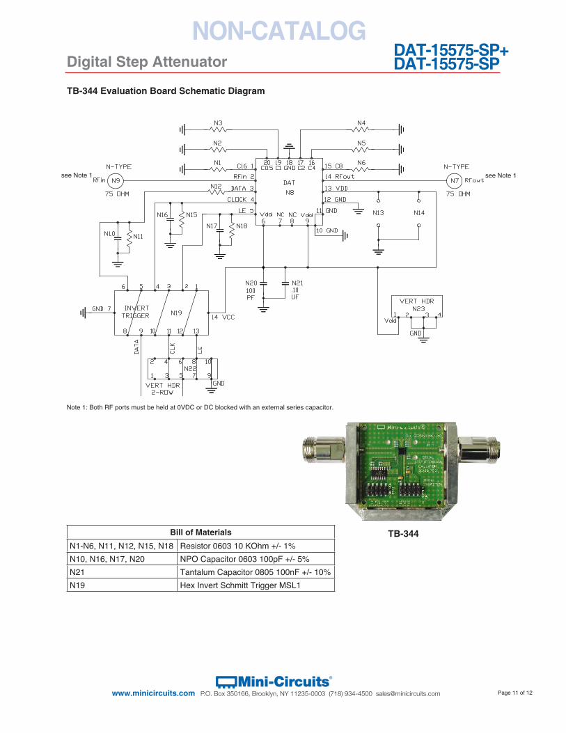
TB-344 Evaluation Board Schematic Diagram
TB-344Bill of MaterialsN1-N6, N11, N12, N15, N18 Resistor 0603 10 KOhm +/- 1%
N10, N16, N17, N20 NPO Capacitor 0603 100pF +/- 5%
N21 Tantalum Capacitor 0805 100nF +/- 10%
N19 Hex Invert Schmitt Trigger MSL1
Note 1: Both RF ports must be held at 0VDC or DC blocked with an external series capacitor.
see Note 1see Note 1
Digital Step Attenuator
Page 12 of 12
DAT-15575-SPDAT-15575-SP+
Mini-Circuits®
www.minicircuits.com P.O. Box 350166, Brooklyn, NY 11235-0003 (718) 934-4500 [email protected]
NON-CATALOG
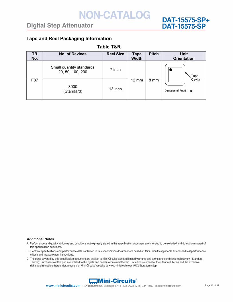
Tape and Reel Packaging Information Table T&R
TRNo.
No. of Devices Reel Size TapeWidth
Pitch Unit Orientation
Small quantity standards 20, 50, 100, 200 7 inch
F873000
(Standard) 13 inch
12 mm 8 mm TapeCavity
Direction of Feed
Additional NotesA. Performance and quality attributes and conditions not expressly stated in this specification document are intended to be excluded and do not form a part of
this specification document. B. Electrical specifications and performance data contained in this specification document are based on Mini-Circuit’s applicable established test performance
criteria and measurement instructions. C. The parts covered by this specification document are subject to Mini-Circuits standard limited warranty and terms and conditions (collectively, “Standard
Terms”); Purchasers of this part are entitled to the rights and benefits contained therein. For a full statement of the Standard Terms and the exclusive rights and remedies thereunder, please visit Mini-Circuits’ website at www.minicircuits.com/MCLStore/terms.jsp