NAU8224 3.1W Stereo Filter-Free Class-D Audio Amplifier ... · with 2 wire interface gain control 1...
27
NAU8224 Datasheet Rev 1.0 Page 1 of 27 Aug, 2012 NAU8224 3.1W Stereo Filter-Free Class-D Audio Amplifier with 2 wire interface gain control 1 Description The NAU8224 is a stereo high efficiency filter-free Class-D audio amplifier, which is capable of driving a 4Ω load with up to 3.1W output power. This device provides chip enable pin with extremely low standby current and fast start-up time of 3.4ms. The NAU8224 features a highly flexible 2 wire interface with many useful gain settings. The gain can be selected from 24dB to -62dB (plus mute) by using 2 wire interface and GS pin. The NAU8224 is ideal for the portable applications of battery drive, as it has advanced features like 87dB PSRR, 91% efficiency, ultra low quiescent current (i.e. 2.1mA at 3.7V for 2 channels) and superior EMI performance. It has the ability to configure the inputs in either single-ended or differential mode. NAU8224 is available in Miniature QFN-20 package. Key Features Low Quiescent Current: • 2.1mA at 3.7V for 2 channels • 3.2mA at 5V for 2 channels Gain Setting with 2 wire interface and GS pin • 24dB to -62dB (plus mute) Powerful Stereo Class-D Amplifier: • 2ch x 3.1W (4Ω @ 5V, 10% THD+N) • 2ch x 1.26W (4Ω @ 3.7V, 1% THD+N) • 2ch x 1.76W (8Ω @ 5V, 10% THD+N) • 2ch x 0.76W (8Ω @ 3.7V, 1% THD+N) Low Output Noise: 20 μV RMS @0dB gain 87dB PSRR @217Hz Low Current Shutdown Mode Click-and Pop Suppression Applications Notebooks / Tablet PCs Personal Media Players / Portable TVs MP3 Players Portable Game Players Digital Camcorders Figure 1: NAU8224Block Diagram
Transcript of NAU8224 3.1W Stereo Filter-Free Class-D Audio Amplifier ... · with 2 wire interface gain control 1...
NAU8224 Datasheet Rev 1.0 Page 1 of 27 Aug, 2012
NAU8224 3.1W Stereo Filter-Free Class-D Audio Amplifier
with 2 wire interface gain control
1 Description The NAU8224 is a stereo high efficiency filter-free Class-D audio amplifier, which is capable of driving a 4Ω load with up to 3.1W output power. This device provides chip enable pin with extremely low standby current and fast start-up time of 3.4ms. The NAU8224 features a highly flexible 2 wire interface with many useful gain settings. The gain can be selected from 24dB to -62dB (plus mute) by using 2 wire interface and GS pin.
The NAU8224 is ideal for the portable applications of battery drive, as it has advanced features like 87dB PSRR, 91% efficiency, ultra low quiescent current (i.e. 2.1mA at 3.7V for 2 channels) and superior EMI performance. It has the ability to configure the inputs in either single-ended or differential mode. NAU8224 is available in Miniature QFN-20 package.
Key Features
Low Quiescent Current:
• 2.1mA at 3.7V for 2 channels
• 3.2mA at 5V for 2 channels Gain Setting with 2 wire interface and GS pin
• 24dB to -62dB (plus mute) Powerful Stereo Class-D Amplifier:
• 2ch x 3.1W (4Ω @ 5V, 10% THD+N)
• 2ch x 1.26W (4Ω @ 3.7V, 1% THD+N)
• 2ch x 1.76W (8Ω @ 5V, 10% THD+N)
• 2ch x 0.76W (8Ω @ 3.7V, 1% THD+N)
Low Output Noise: 20 µVRMS @0dB gain 87dB PSRR @217Hz Low Current Shutdown Mode Click-and Pop Suppression
Applications Notebooks / Tablet PCs Personal Media Players / Portable TVs MP3 Players Portable Game Players Digital Camcorders
Figure 1: NAU8224Block Diagram
NAU8224Datasheet Rev 1.0 Page 2 of 27 Aug, 2012
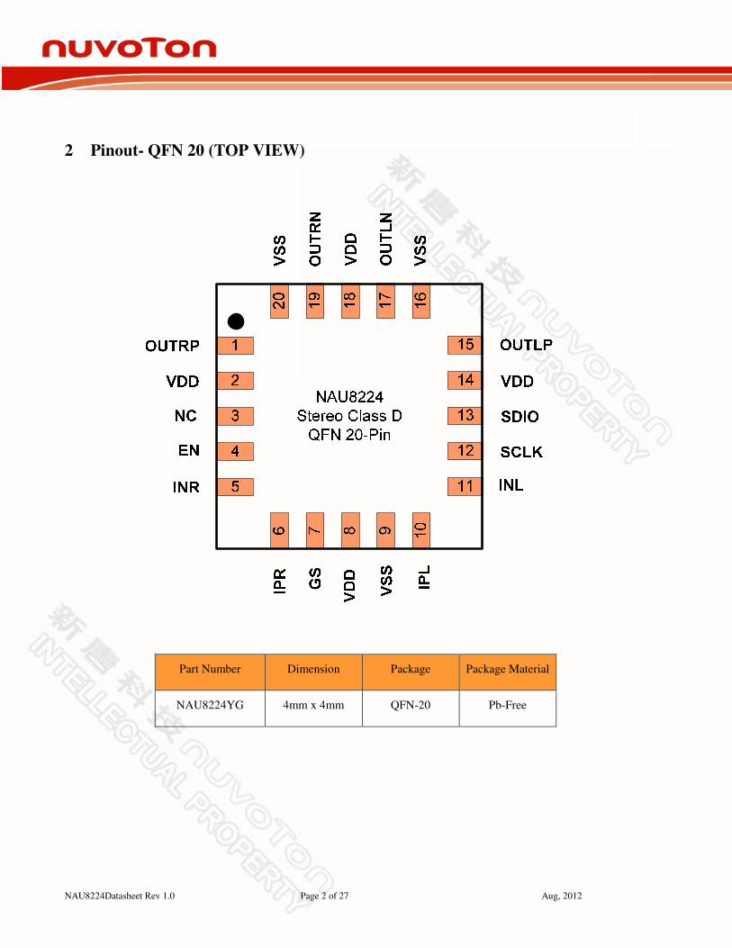
2 Pinout- QFN 20 (TOP VIEW)
Part Number Dimension Package Package Material
NAU8224YG 4mm x 4mm QFN-20 Pb-Free
NAU8224Datasheet Rev 1.0 Page 3 of 27 Aug, 2012
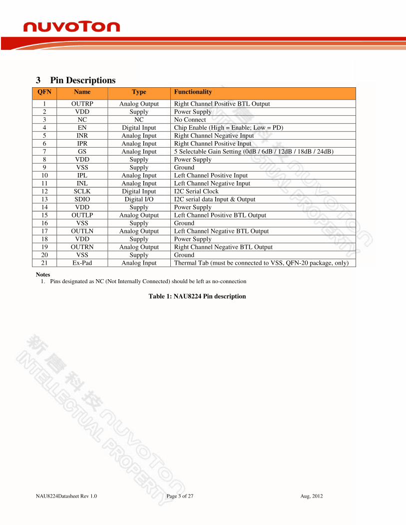
3 Pin Descriptions
QFN Name Type Functionality
1 OUTRP Analog Output Right Channel Positive BTL Output
2 VDD Supply Power Supply
3 NC NC No Connect
4 EN Digital Input Chip Enable (High = Enable; Low = PD)
5 INR Analog Input Right Channel Negative Input
6 IPR Analog Input Right Channel Positive Input
7 GS Analog Input 5 Selectable Gain Setting (0dB / 6dB / 12dB / 18dB / 24dB)
8 VDD Supply Power Supply
9 VSS Supply Ground
10 IPL Analog Input Left Channel Positive Input
11 INL Analog Input Left Channel Negative Input
12 SCLK Digital Input I2C Serial Clock
13 SDIO Digital I/O I2C serial data Input & Output
14 VDD Supply Power Supply
15 OUTLP Analog Output Left Channel Positive BTL Output
16 VSS Supply Ground
17 OUTLN Analog Output Left Channel Negative BTL Output
18 VDD Supply Power Supply
19 OUTRN Analog Output Right Channel Negative BTL Output
20 VSS Supply Ground
21 Ex-Pad Analog Input Thermal Tab (must be connected to VSS, QFN-20 package, only)
Notes 1. Pins designated as NC (Not Internally Connected) should be left as no-connection
Table 1: NAU8224 Pin description
NAU8224Datasheet Rev 1.0 Page 4 of 27 Aug, 2012
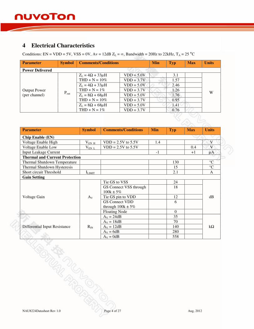
4 Electrical Characteristics
Conditions: EN = VDD = 5V, VSS = 0V, Av = 12dB ZL = ∞, Bandwidth = 20Hz to 22kHz, TA = 25 °C
Parameter Symbol Comments/Conditions Min Typ Max Units
Power Delivered
Output Power
(per channel) Pout
ZL = 4Ω + 33µH
THD + N = 10%
VDD = 5.0V 3.1
W
VDD = 3.7V 1.57
ZL = 4Ω + 33µH
THD + N = 1%
VDD = 5.0V 2.46
VDD = 3.7V 1.26
ZL = 8Ω + 68µH
THD + N = 10%
VDD = 5.0V 1.76
VDD = 3.7V 0.95
ZL = 8Ω + 68µH
THD + N = 1%
VDD = 5.0V 1.41
VDD = 3.7V 0.76
Parameter Symbol Comments/Conditions Min Typ Max Units
Chip Enable (EN)
Voltage Enable High VEN_H VDD = 2.5V to 5.5V 1.4 V
Voltage Enable Low VEN_L VDD = 2.5V to 5.5V 0.4 V
Input Leakage Current -1 +1 µA
Thermal and Current Protection
Thermal Shutdown Temperature 130 °C
Thermal Shutdown Hysteresis 15 °C
Short circuit Threshold ILIMIT 2.1 A
Gain Setting
Voltage Gain AV
Tie GS to VSS 24
dB
GS Connect VSS through
100k ± 5%
18
Tie GS pin to VDD 12
GS Connect VDD
through 100k ± 5%
6
Floating Node 0
Differential Input Resistance RIN
AV = 24dB 35
kΩ
AV = 18dB 70
AV = 12dB 140
AV = 6dB 280
AV = 0dB 558
NAU8224Datasheet Rev 1.0 Page 5 of 27 Aug, 2012
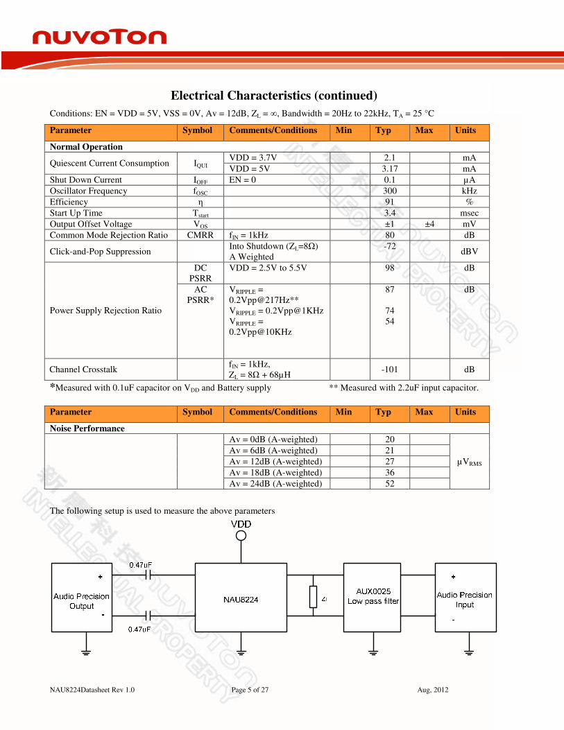
Electrical Characteristics (continued)
Conditions: EN = VDD = 5V, VSS = 0V, Av = 12dB, ZL = ∞, Bandwidth = 20Hz to 22kHz, TA = 25 °C
Parameter Symbol Comments/Conditions Min Typ Max Units
Normal Operation
Quiescent Current Consumption IQUI VDD = 3.7V 2.1 mA
VDD = 5V 3.17 mA
Shut Down Current IOFF EN = 0 0.1 µA
Oscillator Frequency fOSC 300 kHz
Efficiency η 91 %
Start Up Time Tstart 3.4 msec
Output Offset Voltage VOS ±1 ±4 mV
Common Mode Rejection Ratio CMRR fIN = 1kHz 80 dB
Click-and-Pop Suppression Into Shutdown (ZL=8Ω)
A Weighted
-72 dBV
Power Supply Rejection Ratio
DC
PSRR
VDD = 2.5V to 5.5V 98 dB
AC
PSRR*
VRIPPLE =
0.2Vpp@217Hz**
VRIPPLE = 0.2Vpp@1KHz
VRIPPLE =
0.2Vpp@10KHz
87
74
54
dB
Channel Crosstalk fIN = 1kHz,
ZL = 8Ω + 68µH
-101 dB
*Measured with 0.1uF capacitor on VDD and Battery supply ** Measured with 2.2uF input capacitor.
Parameter Symbol Comments/Conditions Min Typ Max Units
Noise Performance
Av = 0dB (A-weighted) 20
µVRMS
Av = 6dB (A-weighted) 21
Av = 12dB (A-weighted) 27
Av = 18dB (A-weighted) 36
Av = 24dB (A-weighted) 52
The following setup is used to measure the above parameters
NAU8224Datasheet Rev 1.0 Page 6 of 27 Aug, 2012
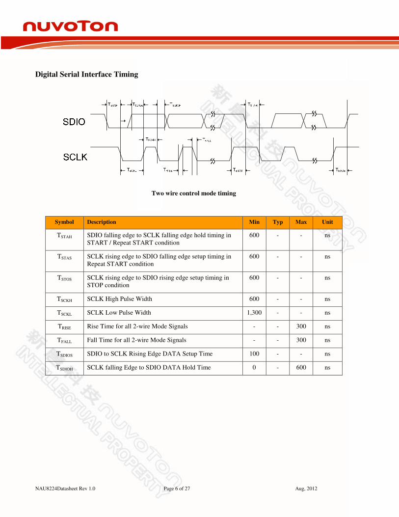
Digital Serial Interface Timing
Two wire control mode timing
Symbol Description Min Typ Max Unit
TSTAH SDIO falling edge to SCLK falling edge hold timing in
START / Repeat START condition
600 - - ns
TSTAS SCLK rising edge to SDIO falling edge setup timing in
Repeat START condition
600 - - ns
TSTOS SCLK rising edge to SDIO rising edge setup timing in
STOP condition
600 - - ns
TSCKH SCLK High Pulse Width 600 - - ns
TSCKL SCLK Low Pulse Width 1,300 - - ns
TRISE Rise Time for all 2-wire Mode Signals - - 300 ns
TFALL Fall Time for all 2-wire Mode Signals - - 300 ns
TSDIOS SDIO to SCLK Rising Edge DATA Setup Time 100 - - ns
TSDIOH SCLK falling Edge to SDIO DATA Hold Time 0 - 600 ns
NAU8224Datasheet Rev 1.0 Page 7 of 27 Aug, 2012
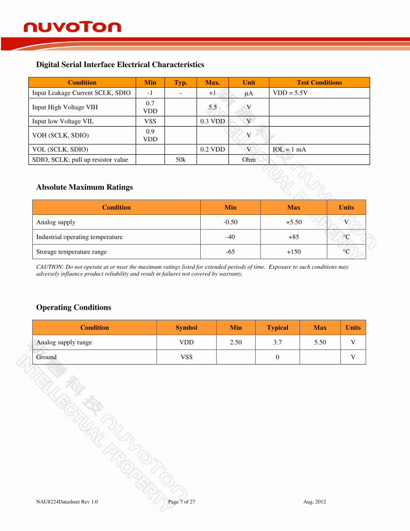
Digital Serial Interface Electrical Characteristics
Condition Min Typ. Max. Unit Test Conditions
Input Leakage Current SCLK, SDIO -1 - +1 µA VDD = 5.5V
Input High Voltage VIH 0.7
VDD 5.5 V
Input low Voltage VIL VSS 0.3 VDD V
VOH (SCLK, SDIO) 0.9
VDD V
VOL (SCLK, SDIO) 0.2 VDD V IOL = 1 mA
SDIO, SCLK; pull up resistor value 50k Ohm
Absolute Maximum Ratings
Condition Min Max Units
Analog supply -0.50 +5.50 V
Industrial operating temperature -40 +85 °C
Storage temperature range -65 +150 °C
CAUTION: Do not operate at or near the maximum ratings listed for extended periods of time. Exposure to such conditions may
adversely influence product reliability and result in failures not covered by warranty.
Operating Conditions
Condition Symbol Min Typical Max Units
Analog supply range VDD 2.50 3.7 5.50 V
Ground VSS 0 V
NAU8224Datasheet Rev 1.0 Page 8 of 27 Aug, 2012
6 Special Feature Description
The NAU8224 offers excellent quantity performance as high efficiency, high output power and low quiescent current. It
also provides the following special features.
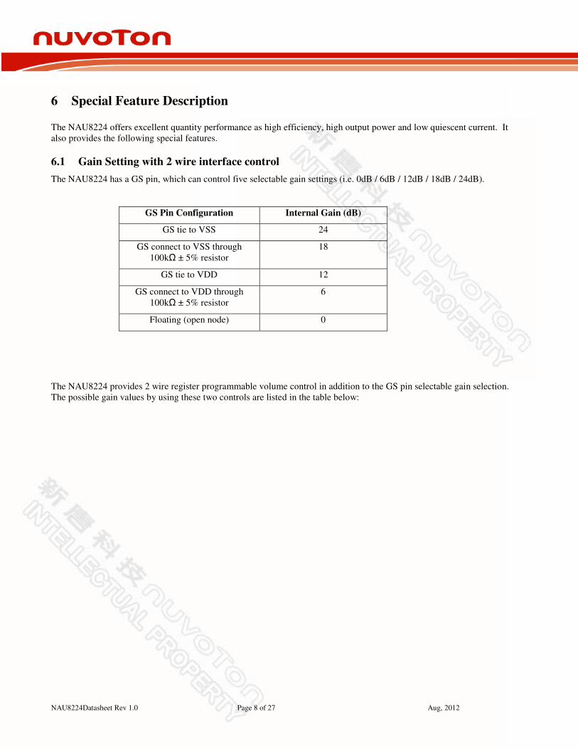
6.1 Gain Setting with 2 wire interface control
The NAU8224 has a GS pin, which can control five selectable gain settings (i.e. 0dB / 6dB / 12dB / 18dB / 24dB).
GS Pin Configuration Internal Gain (dB)
GS tie to VSS 24
GS connect to VSS through
100kΩ ± 5% resistor
18
GS tie to VDD 12
GS connect to VDD through
100kΩ ± 5% resistor
6
Floating (open node) 0
The NAU8224 provides 2 wire register programmable volume control in addition to the GS pin selectable gain selection.
The possible gain values by using these two controls are listed in the table below:
NAU8224Datasheet Rev 1.0 Page 9 of 27 Aug, 2012
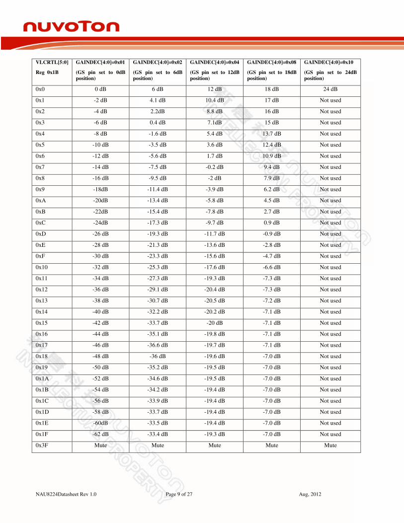
VLCRTL[5:0]
Reg 0x1B
GAINDEC[4:0]=0x01
(GS pin set to 0dB
position)
GAINDEC[4:0]=0x02
(GS pin set to 6dB
position)
GAINDEC[4:0]=0x04
(GS pin set to 12dB
position)
GAINDEC[4:0]=0x08
(GS pin set to 18dB
position)
GAINDEC[4:0]=0x10
(GS pin set to 24dB
position)
0x0 0 dB 6 dB 12 dB 18 dB 24 dB
0x1 -2 dB 4.1 dB 10.4 dB 17 dB Not used
0x2 -4 dB 2.2dB 8.8 dB 16 dB Not used
0x3 -6 dB 0.4 dB 7.1dB 15 dB Not used
0x4 -8 dB -1.6 dB 5.4 dB 13.7 dB Not used
0x5 -10 dB -3.5 dB 3.6 dB 12.4 dB Not used
0x6 -12 dB -5.6 dB 1.7 dB 10.9 dB Not used
0x7 -14 dB -7.5 dB -0.2 dB 9.4 dB Not used
0x8 -16 dB -9.5 dB -2 dB 7.9 dB Not used
0x9 -18dB -11.4 dB -3.9 dB 6.2 dB Not used
0xA -20dB -13.4 dB -5.8 dB 4.5 dB Not used
0xB -22dB -15.4 dB -7.8 dB 2.7 dB Not used
0xC -24dB -17.3 dB -9.7 dB 0.9 dB Not used
0xD -26 dB -19.3 dB -11.7 dB -0.9 dB Not used
0xE -28 dB -21.3 dB -13.6 dB -2.8 dB Not used
0xF -30 dB -23.3 dB -15.6 dB -4.7 dB Not used
0x10 -32 dB -25.3 dB -17.6 dB -6.6 dB Not used
0x11 -34 dB -27.3 dB -19.3 dB -7.3 dB Not used
0x12 -36 dB -29.1 dB -20.4 dB -7.3 dB Not used
0x13 -38 dB -30.7 dB -20.5 dB -7.2 dB Not used
0x14 -40 dB -32.2 dB -20.2 dB -7.1 dB Not used
0x15 -42 dB -33.7 dB -20 dB -7.1 dB Not used
0x16 -44 dB -35.1 dB -19.8 dB -7.1 dB Not used
0x17 -46 dB -36.6 dB -19.7 dB -7.1 dB Not used
0x18 -48 dB -36 dB -19.6 dB -7.0 dB Not used
0x19 -50 dB -35.2 dB -19.5 dB -7.0 dB Not used
0x1A -52 dB -34.6 dB -19.5 dB -7.0 dB Not used
0x1B -54 dB -34.2 dB -19.4 dB -7.0 dB Not used
0x1C -56 dB -33.9 dB -19.4 dB -7.0 dB Not used
0x1D -58 dB -33.7 dB -19.4 dB -7.0 dB Not used
0x1E -60dB -33.5 dB -19.4 dB -7.0 dB Not used
0x1F -62 dB -33.4 dB -19.3 dB -7.0 dB Not used
0x3F Mute Mute Mute Mute Mute
NAU8224Datasheet Rev 1.0 Page 10 of 27 Aug, 2012
6.1.1 2-Wire-Serial Control and Data Bus (I2C Style Interface)
The serial interface provides a 2-wire bidirectional read/write data interface similar to and typically compatible with
standard I2C protocol. This protocol defines any device that sends CLK onto the bus as a master, and the receiving
device as slave. The NAU8224 can function only as a slave device.
An external clock drives the device, and in accordance with the protocol, data is sent to or from the device accordingly.
All functions are controlled by means of a register control interface in the device.
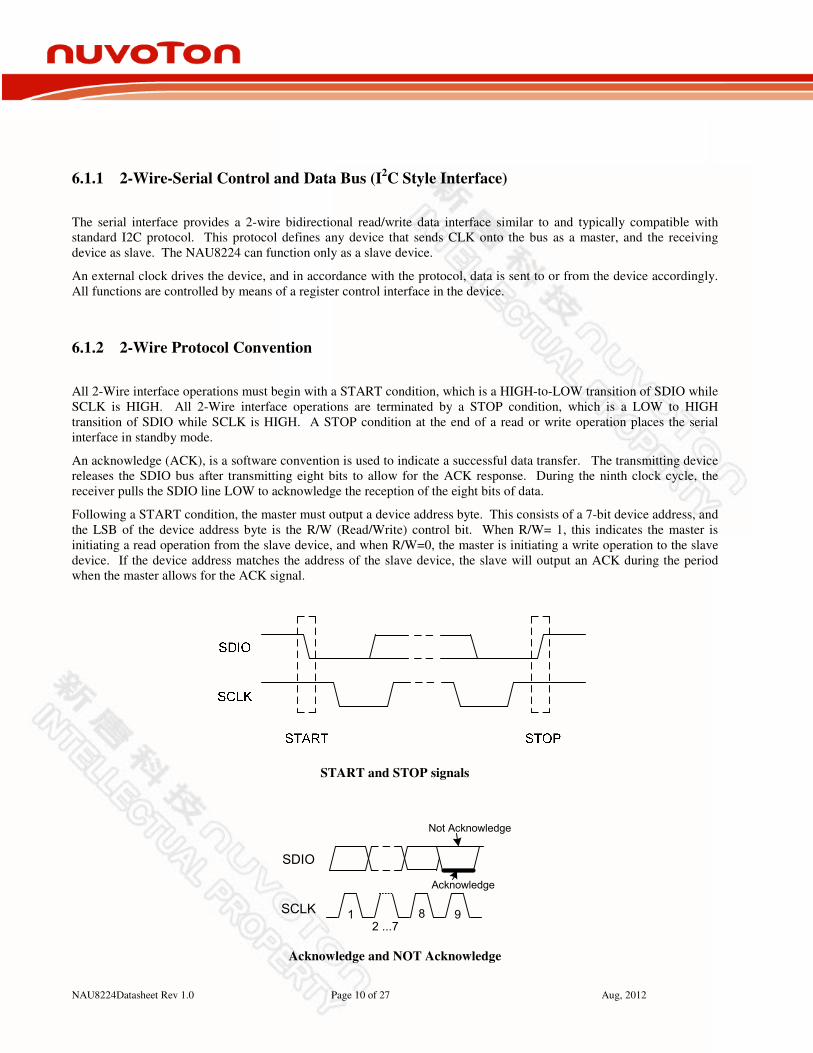
6.1.2 2-Wire Protocol Convention
All 2-Wire interface operations must begin with a START condition, which is a HIGH-to-LOW transition of SDIO while
SCLK is HIGH. All 2-Wire interface operations are terminated by a STOP condition, which is a LOW to HIGH
transition of SDIO while SCLK is HIGH. A STOP condition at the end of a read or write operation places the serial
interface in standby mode.
An acknowledge (ACK), is a software convention is used to indicate a successful data transfer. The transmitting device
releases the SDIO bus after transmitting eight bits to allow for the ACK response. During the ninth clock cycle, the
receiver pulls the SDIO line LOW to acknowledge the reception of the eight bits of data.
Following a START condition, the master must output a device address byte. This consists of a 7-bit device address, and
the LSB of the device address byte is the R/W (Read/Write) control bit. When R/W= 1, this indicates the master is
initiating a read operation from the slave device, and when R/W=0, the master is initiating a write operation to the slave
device. If the device address matches the address of the slave device, the slave will output an ACK during the period
when the master allows for the ACK signal.
START and STOP signals
9812 ...7
Acknowledge
SCLK
SDIO
Not Acknowledge
Acknowledge and NOT Acknowledge
NAU8224Datasheet Rev 1.0 Page 11 of 27 Aug, 2012
Device
Address Byte
Control
Address Byte
Data Byte
0 1 0 1 0 1 0 R/W
A7 A6 A5 A4 A3 A2 A1 A0
D7 D6 D5 D4 D3 D2 D1 D0
Slave Address Byte, Control Address Byte, and Data Byte
6.1.3 2-Wire Write Operation
A Write operation consists of a two-byte instruction followed by a Data Byte. A Write operation requires a START
condition, followed by a valid device address byte with R/W= 0, a valid control address byte, data byte, and a STOP
condition.
The NAU8224 is permanently programmed with “010 1010” (0x2A) as the Device Address. If the Device Address
matches this value, the NAU8224 will respond with the expected ACK signaling as it accepts the data being transmitted
into it.
Write Sequence
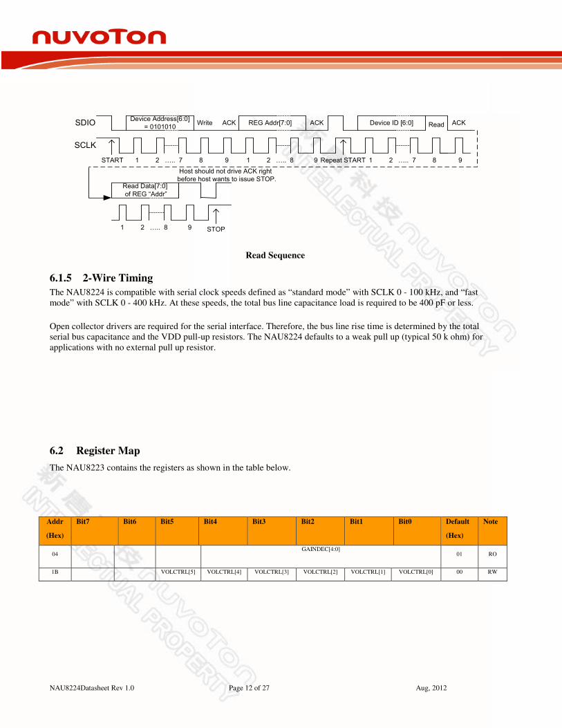
6.1.4 2-Wire Single Read Operation
A Read operation consists of a three-byte Write instruction followed by a Read instruction of data byte. The bus master
initiates the operation issuing the following sequence: a START condition, device address byte with the R/W bit set to
“0”, and a Control Register Address byte. This indicates to the slave device which of its control registers is to be
accessed.
The NAU8224 is permanently programmed with “010 1010” (0x2A) as its device address. If the device address matches
this value, the NAU8224 will respond with the expected ACK signaling as it accepts the Control Register Address being
transmitted into it. After this, the master transmits a second START condition, and a second instantiation of the same
device address, but now with R/W=1.
After again recognizing its device address, the NAU8224 transmits an ACK, followed by a one byte value containing the
data from the selected control register inside the NAU8224. During this phase, the master generates the ACK signaling
with byte transferred from the NAU8224.
NAU8224Datasheet Rev 1.0 Page 12 of 27 Aug, 2012
ACK ACK
START
Device Address[6:0]
= 0101010REG Addr[7:0]Write Device ID [6:0] Read
Repeat START
ACK
Read Data[7:0]
of REG “Addr”
Host should not drive ACK right
before host wants to issue STOP.
SCLK
SDIO
1 2 ….. 7 8 9
1 2 ….. 8 9
1 2 ….. 8 9 1 2 ….. 7 8 9
STOP
Read Sequence
6.1.5 2-Wire Timing
The NAU8224 is compatible with serial clock speeds defined as “standard mode” with SCLK 0 - 100 kHz, and “fast
mode” with SCLK 0 - 400 kHz. At these speeds, the total bus line capacitance load is required to be 400 pF or less.
Open collector drivers are required for the serial interface. Therefore, the bus line rise time is determined by the total
serial bus capacitance and the VDD pull-up resistors. The NAU8224 defaults to a weak pull up (typical 50 k ohm) for
applications with no external pull up resistor.
6.2 Register Map
The NAU8223 contains the registers as shown in the table below.
Addr
(Hex)
Bit7 Bit6 Bit5 Bit4 Bit3 Bit2 Bit1 Bit0 Default
(Hex)
Note
04
GAINDEC[4:0]
01 RO
1B
VOLCTRL[5] VOLCTRL[4] VOLCTRL[3] VOLCTRL[2] VOLCTRL[1] VOLCTRL[0] 00 RW
NAU8224Datasheet Rev 1.0 Page 13 of 27 Aug, 2012
6.3 Register Map Details
0x04:REGGAIN
This register is a read only register and can be used to check the function of the GAIN pin.
Bit Default Function when read ‘1’
GAINDEC[4] 0 24 dB Gain setting enabled
GAINDEC[3] 0 18 dB Gain setting enabled
GAINDEC[2] 0 12 dB Gain setting enabled
GAINDEC[1] 0 6 dB Gain setting enabled
GAINDEC[0] 0 0 dB Gain setting enabled
0x1B: VOLCTRL[5:0]
This register can be used to adjust the output volume.
Bit Default Function when set to ‘1’
VOLCTRL[5] 0 Adjust Output Volume
VOLCTRL[4] 0 Adjust Output Volume
VOLCTRL[3] 0 Adjust Output Volume
VOLCTRL[2] 0 Adjust Output Volume
VOLCTRL[1] 0 Adjust Output Volume
VOLCTRL[0] 0 Adjust Output Volume
6.4 Device Protection
The NAU8224 includes device protection for three operating scenarios. They are
1. Thermal Overload
2. Short circuit
3. Supply under voltage
6.4.1 Thermal Overload Protection
When the device internal junction temperature reaches 130°C, the NAU8224 will disable the output drivers. When the
device cools down and a safe operating temperature of 115°C has been reached for at least about 47ms, the output
drivers will be enabled again.
6.4.2 Short Circuit Protection
If a short circuit is detected on any of the pull-up or pull-down devices on the output drivers for at least 14µs, the output
drivers will be disabled for 47ms. The output drivers will then be enabled again and check for the short circuit. If the
NAU8224Datasheet Rev 1.0 Page 14 of 27 Aug, 2012
short circuit is still present, the output drivers are disabled after 14µs. This cycle will continue until the short circuit is
removed. The short circuit threshold is set at 2.1A.
6.4.3 Supply under Voltage Protection
If the supply voltage drops under 2.1V, the output drivers will be disabled while the NAU8224 control circuitry still
operates. This will avoid the battery supply to drag down too low before the host processor can safely shut down the
devices on the system. If the supply drops further below 1.0V the internal power on reset activated and puts the entire
device in power down state.
6.5 Power up and Power down Control
When the supply voltage ramps up, the internal power on reset circuit gets triggered. At this time all internal circuits will
be set to power down state. The device can be enabled by setting the EN pin high. Upon setting the EN pin high, the
device will go through an internal power up sequence in order to minimize ‘pops’ on the speaker output. The complete
power up sequence will take about 3.4ms. The device will power down in about 30µs, when the EN pin is set low.
It is important to keep the input signal at zero amplitude or enable the mute condition in order to minimize the ‘pops’
when the EN pin is toggled.
.
NAU8224Datasheet Rev 1.0 Page 15 of 27 Aug, 2012
7 Typical Operating Characteristics Conditions: EN = VDD = 5V, VSS = 0V, Av = 12dB, ZL = ∞, Bandwidth = 20Hz to 22kHz, TA = 25°C, unless otherwise
noted
0
10
20
30
40
50
60
70
80
90
100
0 1 2 3 4
Eff
icie
ncy
(%)
Output Power(W)
Efficiency Vs Output Power
(VDD = 5.0V)
ZL=4Ω+33uH
ZL=8Ω+68uH
0
10
20
30
40
50
60
70
80
90
100
0 0.5 1 1.5 2
Eff
icie
ncy
(%)
Output Power(W)
Efficiency Vs Output Power
(VDD = 3.7V)
ZL=4Ω+ 33uH
ZL=8Ω +68uH
0.001
0.01
0.1
1
20 200 2000 20000
TH
D+
N(%
)
Frequency(Hz)
THD+N vs Frequency
(VDD = 3.7V, ZL= 8Ω + 68uH)
Pout 0.2W
Pout 0.4W
0.001
0.01
0.1
1
20 200 2000 20000
TH
D+
N(%
)
Frequency(Hz)
THD+N vs Frequency
(VDD = 4.2V, ZL= 8Ω + 68uH)
Pout 0.2W
Pout 0.6W
NAU8224Datasheet Rev 1.0 Page 16 of 27 Aug, 2012
0.001
0.01
0.1
1
20 200 2000 20000
TH
D+
N(%
)
Frequency(Hz)
THD+N vs Frequency
(VDD = 5V, ZL= 8Ω + 68uH)
Pout 0.2W
Pout 1.2W
0.001
0.01
0.1
1
10
0 0.5 1 1.5
TH
D+
N (
%)
Pout (W)
THD+N vs Pout
(VDD = 3.7V, ZL = 8Ω + 68uH)
f 100Hz
f 1kHz
f 6kHz
0.001
0.01
0.1
1
10
0 0.5 1 1.5 2
TH
D+
N (
%)
Pout (W)
THD+N vs Pout
(VDD = 4.2V, ZL= 8Ω + 68uH)
f 100Hz
f 1kHz
f 6kHz
0.001
0.01
0.1
1
10
0 1 2 3
TH
D+
N (
%)
Pout (W)
THD+N vs Pout
(VDD = 5V, ZL=8Ω + 68uH)
f 100Hz
f 1kHz
f 6kHz
NAU8224Datasheet Rev 1.0 Page 17 of 27 Aug, 2012
0.001
0.01
0.1
1
20 200 2000 20000
TH
D+
N(%
)
Frequency(Hz)
THD+N vs Frequency
(VDD = 3.7V, ZL= 4Ω + 33uH)
Pout 0.2W
Pout 0.8W
0.001
0.01
0.1
1
20 200 2000 20000
TH
D+
N(%
)
Frequency(Hz)
THD+N vs Frequency
(VDD = 4.2V, ZL= 4Ω + 33uH)
Pout 0.2W
Pout 1W
0.001
0.01
0.1
1
20 200 2000 20000
TH
D+
N(%
)
Frequency (Hz)
THD+N vs Frequency
(VDD = 5V, ZL= 4Ω + 33uH)
Pout 1.5W
Pout 2W
0.001
0.01
0.1
1
10
0 1 2 3
TH
D+
N (
%)
Pout (W)
THD+N vs Pout
(VDD = 3.7V, ZL= 4Ω + 33uH)
f = 100Hz
f = 1kHz
f = 6kHz
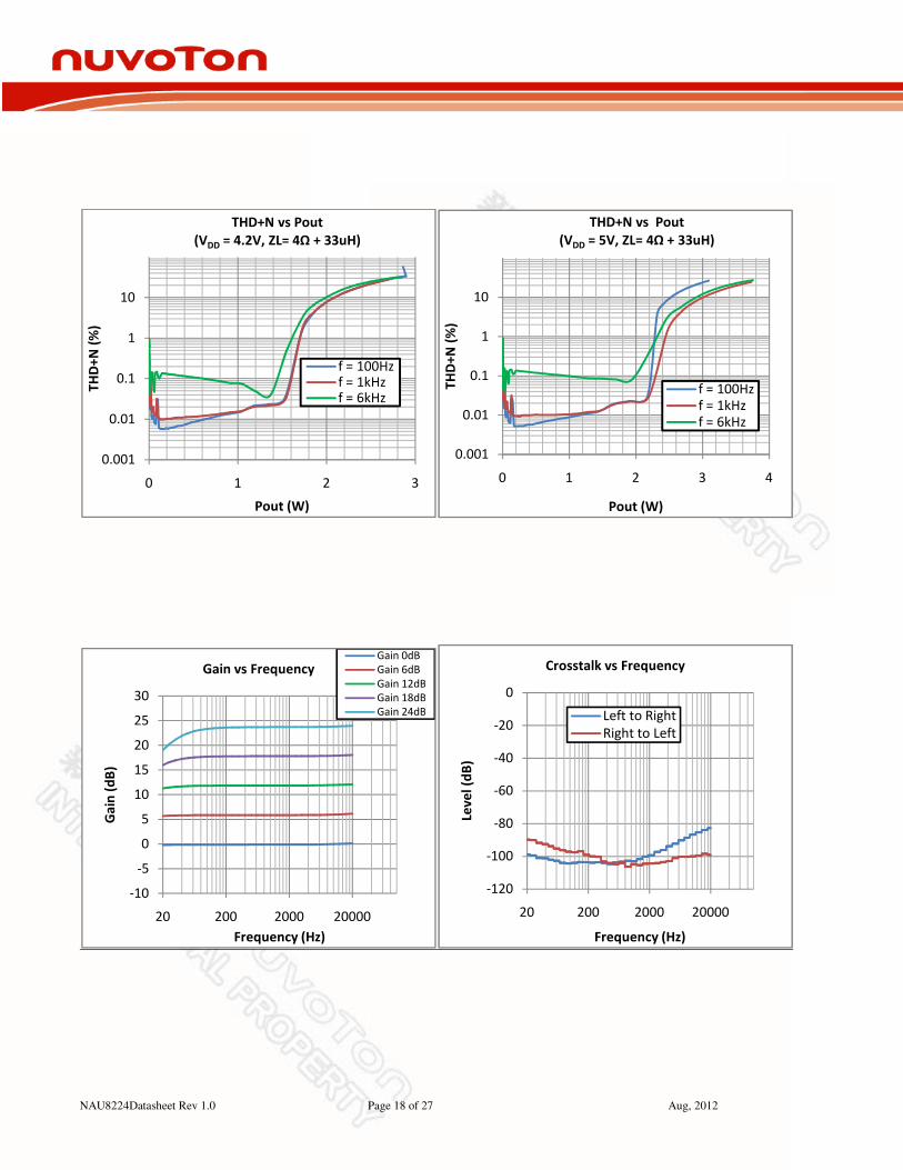
NAU8224Datasheet Rev 1.0 Page 18 of 27 Aug, 2012
0.001
0.01
0.1
1
10
0 1 2 3
TH
D+
N (
%)
Pout (W)
THD+N vs Pout
(VDD = 4.2V, ZL= 4Ω + 33uH)
f = 100Hzf = 1kHzf = 6kHz
0.001
0.01
0.1
1
10
0 1 2 3 4
TH
D+
N (
%)
Pout (W)
THD+N vs Pout
(VDD = 5V, ZL= 4Ω + 33uH)
f = 100Hz
f = 1kHz
f = 6kHz
-10
-5
0
5
10
15
20
25
30
20 200 2000 20000
Ga
in (
dB
)
Frequency (Hz)
Gain vs FrequencyGain 0dB
Gain 6dB
Gain 12dB
Gain 18dB
Gain 24dB
-120
-100
-80
-60
-40
-20
0
20 200 2000 20000
Lev
el
(dB
)
Frequency (Hz)
Crosstalk vs Frequency
Left to Right
Right to Left
NAU8224Datasheet Rev 1.0
-100
-90
-80
-70
-60
-50
-40
-30
-20
-10
0
2.5 3.5 4.5
PS
RR
(d
B)
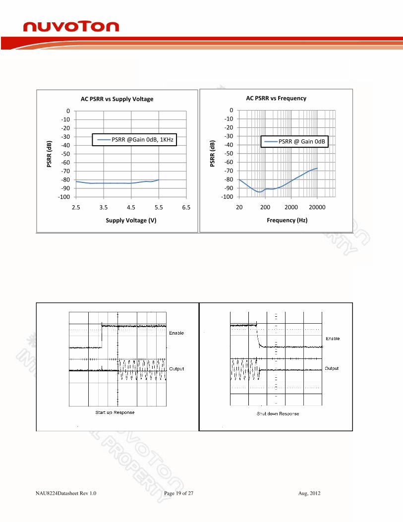
Supply Voltage (V)
AC PSRR vs Supply Voltage
PSRR @Gain 0dB, 1KHz
Page 19 of 27 Aug, 2012
5.5 6.5
Supply Voltage (V)
AC PSRR vs Supply Voltage
PSRR @Gain 0dB, 1KHz
-100
-90
-80
-70
-60
-50
-40
-30
-20
-10
0
20 200 2000P
SR
R (
dB
)
Frequency (Hz)
AC PSRR vs Frequency
PSRR @ Gain 0dB
Aug, 2012
20000
Frequency (Hz)
AC PSRR vs Frequency
PSRR @ Gain 0dB
NAU8224Datasheet Rev 1.0 Page 20 of 27 Aug, 2012
0
0.5
1
1.5
2
2.5
3
3.5
2.5 3.5 4.5 5.5
Su
pp
ly C
urr
en
t(m
A)
Supply Voltage (V)
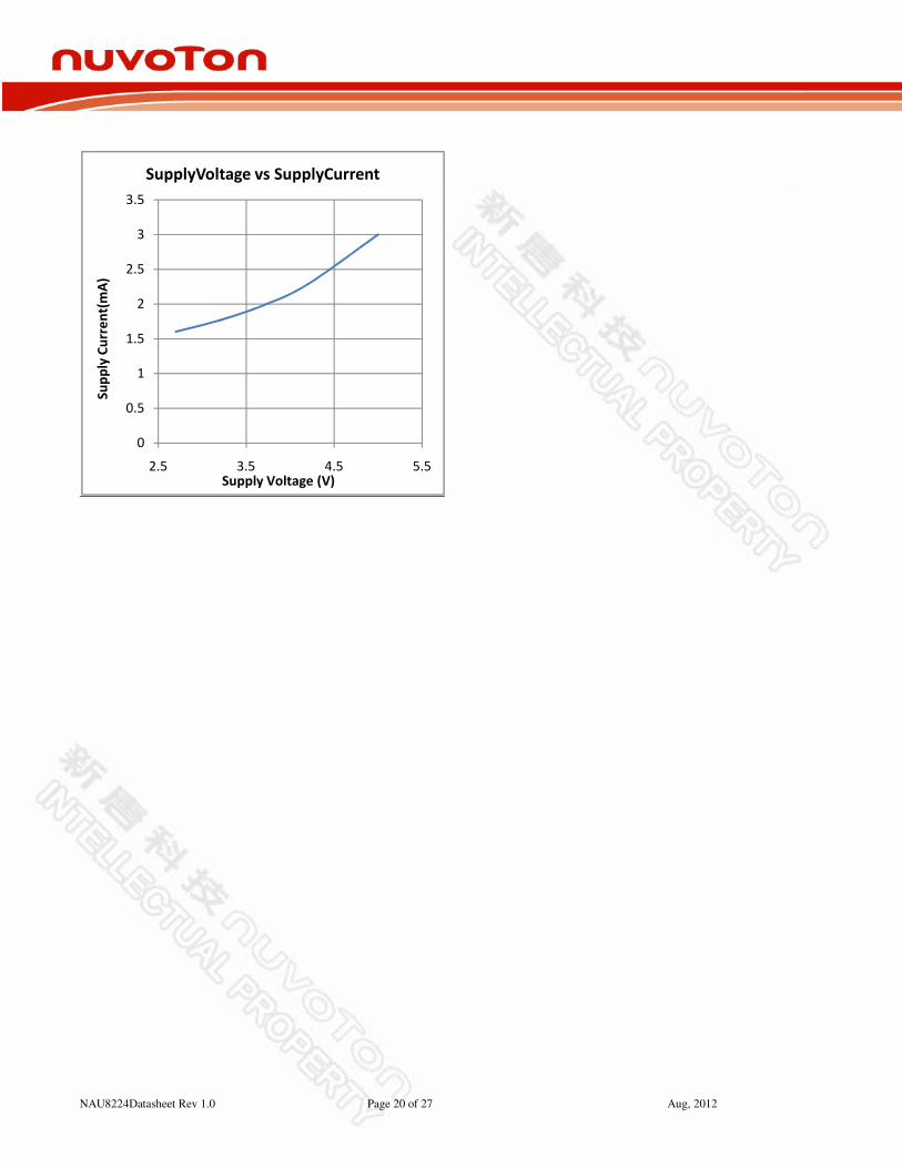
SupplyVoltage vs SupplyCurrent
NAU8224Datasheet Rev 1.0 Page 21 of 27 Aug, 2012
8 Application Information
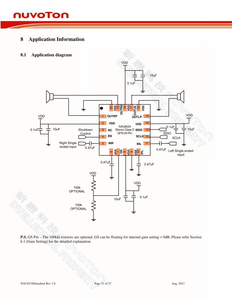
8.1 Application diagram
VS
SOUTLP
VD
D
IPL
VDD
EN
VS
S
VDD
SDIO
GS
VD
D
VS
S
NC
INR
IPR
OU
TLN
SCLK
OU
TR
N
OUTRP
2
3
4
5
6 7 8
1
10
15
14
13
12
11
16
9
20
19
18
17
INL
NAU8224
Stereo Class D
QFN 20-Pin
VDD
100k
OPTIONAL
100k
OPTIONAL
10uF0.1uF
0.47uF0.47uF
0.47uF0.47uF
0.1uF10uF
10uF0.1uF
10uF
0.1uF
VDD
VDDVDD
VDD
Shutdown
Control
Left Single ended
input
Right Single
ended input
SCLK
SDIO
P.S. GS Pin – The 100kΩ resistors are optional. GS can be floating for internal gain setting = 0dB. Please refer Section
6.1 (Gain Setting) for the detailed explanation.
NAU8224Datasheet Rev 1.0 Page 22 of 27 Aug, 2012
8.2 Component selection
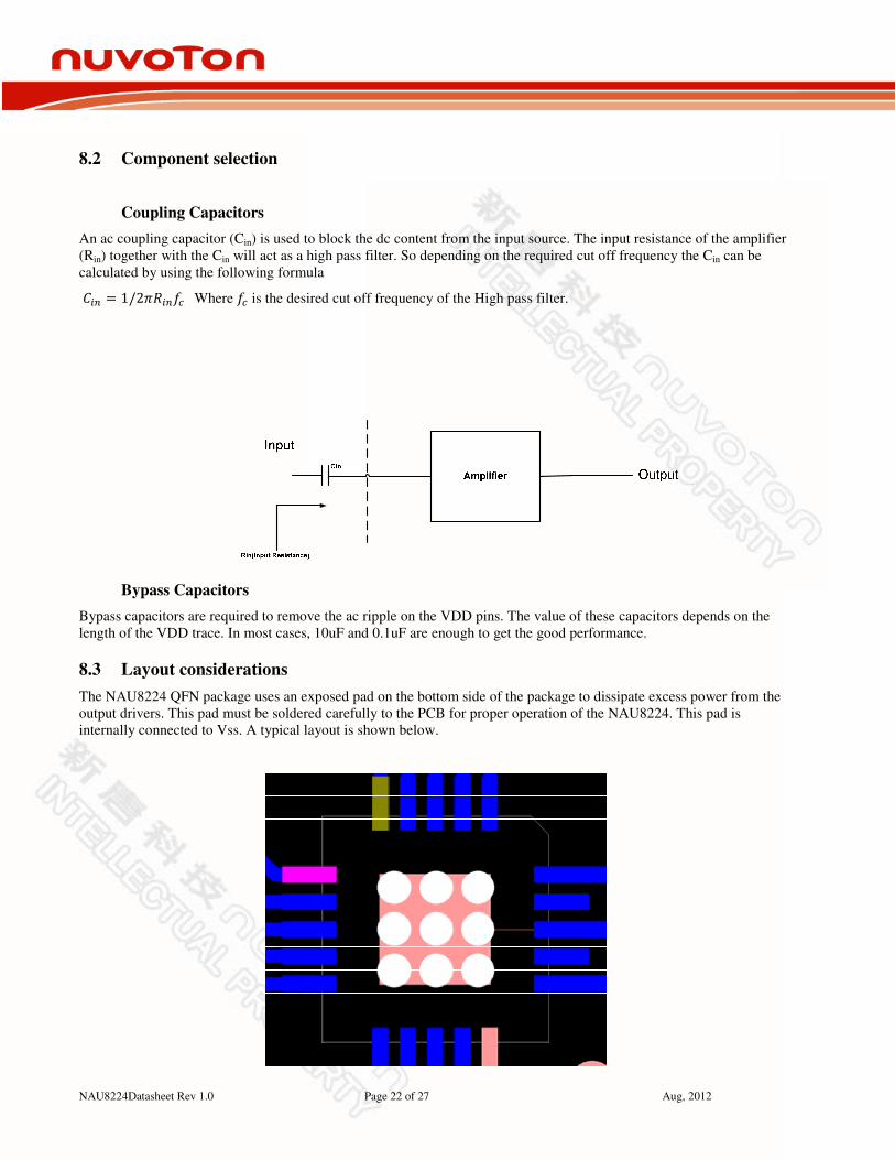
Coupling Capacitors
An ac coupling capacitor (Cin) is used to block the dc content from the input source. The input resistance of the amplifier
(Rin) together with the Cin will act as a high pass filter. So depending on the required cut off frequency the Cin can be
calculated by using the following formula
1/2 Where is the desired cut off frequency of the High pass filter.
Bypass Capacitors
Bypass capacitors are required to remove the ac ripple on the VDD pins. The value of these capacitors depends on the
length of the VDD trace. In most cases, 10uF and 0.1uF are enough to get the good performance.
8.3 Layout considerations
The NAU8224 QFN package uses an exposed pad on the bottom side of the package to dissipate excess power from the
output drivers. This pad must be soldered carefully to the PCB for proper operation of the NAU8224. This pad is
internally connected to Vss. A typical layout is shown below.
NAU8224Datasheet Rev 1.0 Page 23 of 27 Aug, 2012
The PCB has to be designed in such a manner that it should have nine vias in 3x3 grid under NAU8224. The vias should
have hole size of 12mil and a spacing of 30mils. The pad size of the vias is 24mils. The vias on the top side of the board
should be connected with a copper pour that has an area of 2mm x 2mm, centered underneath the NAU8224. The nine
vias should connect to copper pour area on the bottom of the PCB. It is preferred to pour the complete bottom side of the
board with Vss.
Also good PCB layout and grounding techniques are essential to get the good audio performance. It is better to use low
resistance traces as these devices are driving low impedance loads. The resistance of the traces has a significant effect on
the output power delivered to the load. In order to dissipate more heat, use wide traces for the power and ground lines.
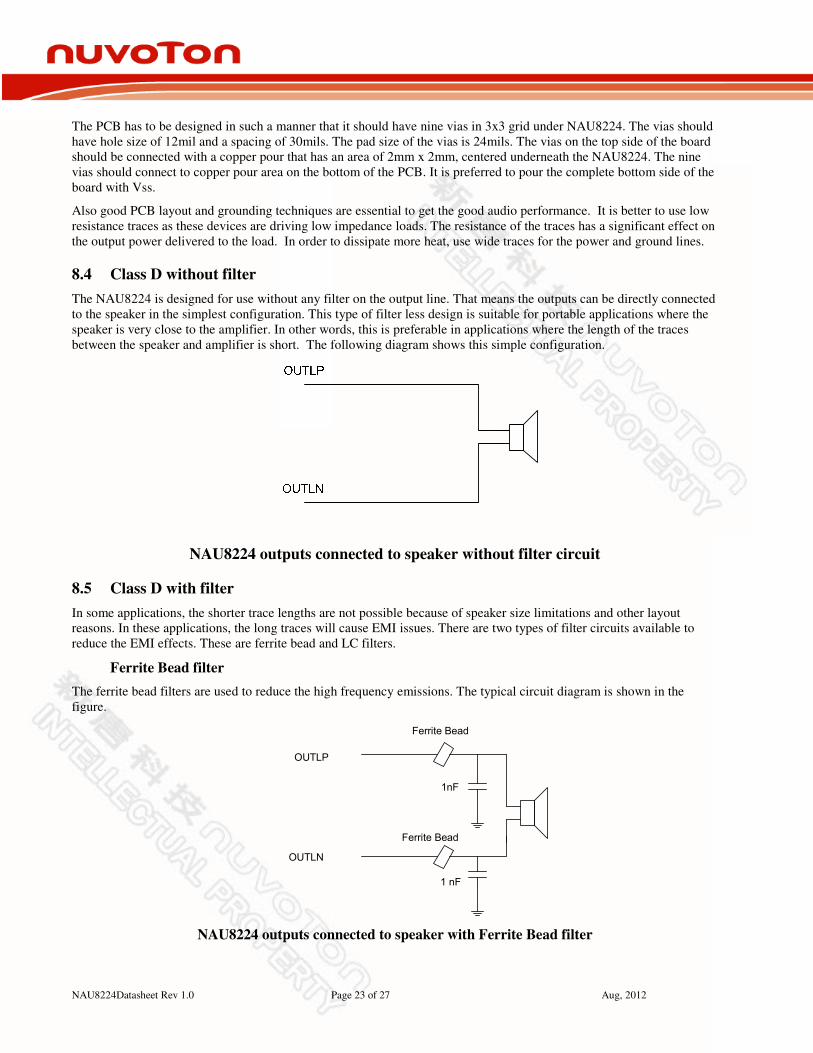
8.4 Class D without filter
The NAU8224 is designed for use without any filter on the output line. That means the outputs can be directly connected
to the speaker in the simplest configuration. This type of filter less design is suitable for portable applications where the
speaker is very close to the amplifier. In other words, this is preferable in applications where the length of the traces
between the speaker and amplifier is short. The following diagram shows this simple configuration.
NAU8224 outputs connected to speaker without filter circuit
8.5 Class D with filter
In some applications, the shorter trace lengths are not possible because of speaker size limitations and other layout
reasons. In these applications, the long traces will cause EMI issues. There are two types of filter circuits available to
reduce the EMI effects. These are ferrite bead and LC filters.
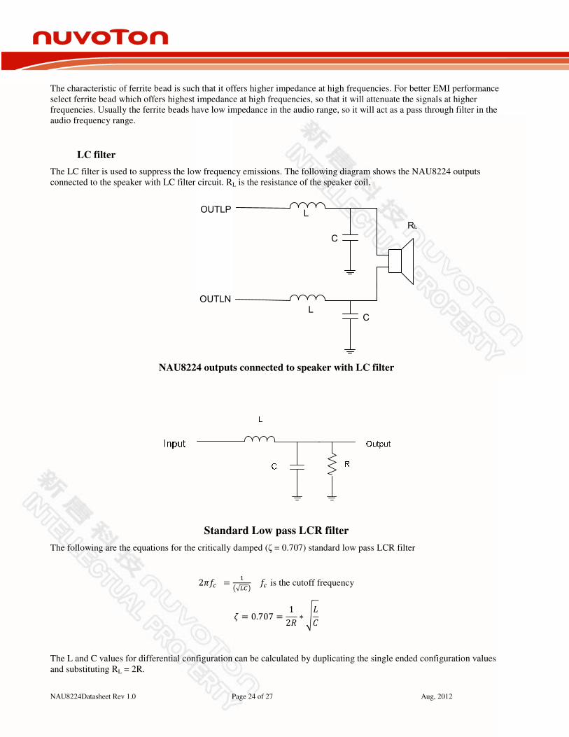
Ferrite Bead filter
The ferrite bead filters are used to reduce the high frequency emissions. The typical circuit diagram is shown in the
figure.
1nF
1 nF
Ferrite Bead
Ferrite Bead
OUTLP
OUTLN
NAU8224 outputs connected to speaker with Ferrite Bead filter
NAU8224Datasheet Rev 1.0 Page 24 of 27 Aug, 2012
The characteristic of ferrite bead is such that it offers higher impedance at high frequencies. For better EMI performance
select ferrite bead which offers highest impedance at high frequencies, so that it will attenuate the signals at higher
frequencies. Usually the ferrite beads have low impedance in the audio range, so it will act as a pass through filter in the
audio frequency range.
LC filter
The LC filter is used to suppress the low frequency emissions. The following diagram shows the NAU8224 outputs
connected to the speaker with LC filter circuit. RL is the resistance of the speaker coil.
OUTLP
OUTLNL
C
C
RL
L
NAU8224 outputs connected to speaker with LC filter
Standard Low pass LCR filter
The following are the equations for the critically damped (ζ = 0.707) standard low pass LCR filter
2 √ is the cutoff frequency
0.707 12
The L and C values for differential configuration can be calculated by duplicating the single ended configuration values
and substituting RL = 2R.
NAU8224Datasheet Rev 1.0 Page 25 of 27 Aug, 2012
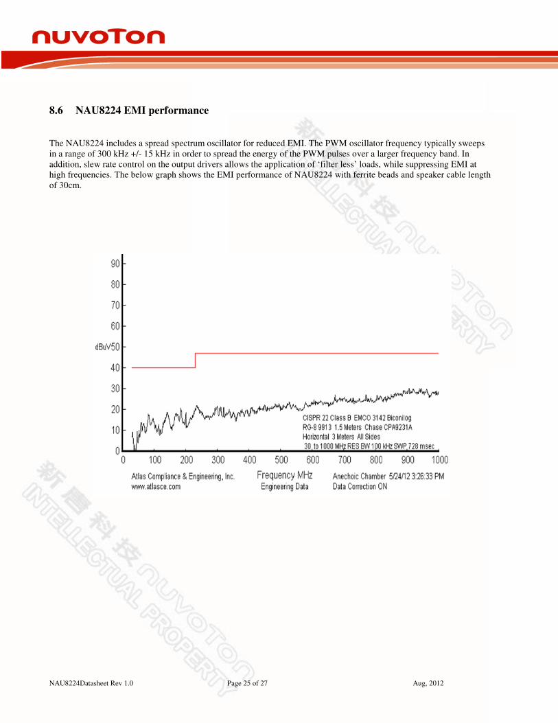
8.6 NAU8224 EMI performance
The NAU8224 includes a spread spectrum oscillator for reduced EMI. The PWM oscillator frequency typically sweeps
in a range of 300 kHz +/- 15 kHz in order to spread the energy of the PWM pulses over a larger frequency band. In
addition, slew rate control on the output drivers allows the application of ‘filter less’ loads, while suppressing EMI at
high frequencies. The below graph shows the EMI performance of NAU8224 with ferrite beads and speaker cable length
of 30cm.
NAU8224Datasheet Rev 1.0 Page 26 of 27 Aug, 2012
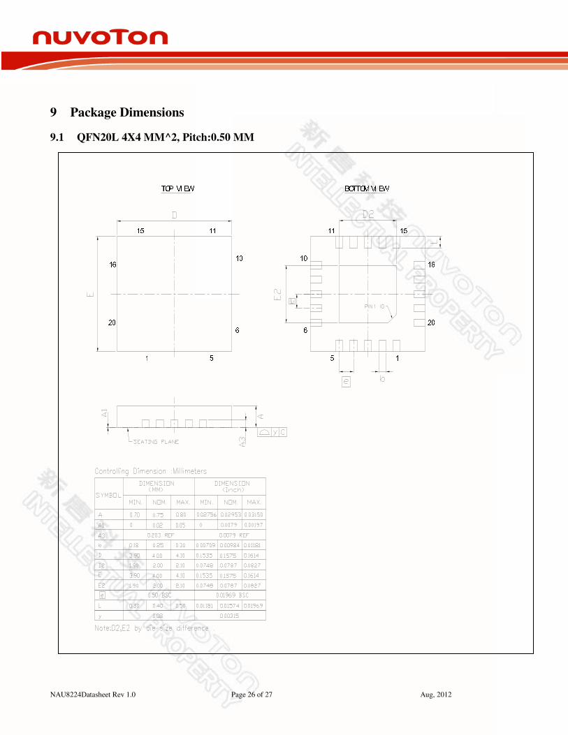
9 Package Dimensions
9.1 QFN20L 4X4 MM^2, Pitch:0.50 MM
TOP VI EW BOTTOM VI EW116 201510 15 1616 15 11 10
65120
NAU8224Datasheet Rev 1.0 Page 27 of 27 Aug, 2012
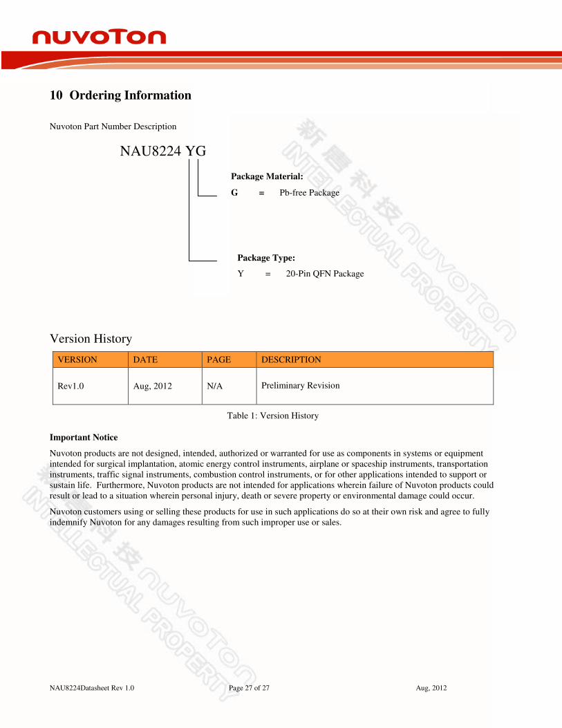
10 Ordering Information
Nuvoton Part Number Description
Version History
VERSION DATE PAGE DESCRIPTION
Rev1.0 Aug, 2012 N/A
Preliminary Revision
Table 1: Version History
Important Notice
Nuvoton products are not designed, intended, authorized or warranted for use as components in systems or equipment
intended for surgical implantation, atomic energy control instruments, airplane or spaceship instruments, transportation
instruments, traffic signal instruments, combustion control instruments, or for other applications intended to support or
sustain life. Furthermore, Nuvoton products are not intended for applications wherein failure of Nuvoton products could
result or lead to a situation wherein personal injury, death or severe property or environmental damage could occur.
Nuvoton customers using or selling these products for use in such applications do so at their own risk and agree to fully
indemnify Nuvoton for any damages resulting from such improper use or sales.
Package Type:
Y = 20-Pin QFN Package
NAU8224 YG
Package Material:
G = Pb-free Package