NaNotechNology - IOPsciencecms.iopscience.iop.org/alfresco/d/d/workspace/SpacesStore/2f0efe10... ·...
32
Highlights from 25 years iopscience.org/nano NANOTECHNOLOGY anniversary N a n o t e c h n o l o g y
Transcript of NaNotechNology - IOPsciencecms.iopscience.iop.org/alfresco/d/d/workspace/SpacesStore/2f0efe10... ·...
Highlights from 25 yearsiopscience.org/nano
NaNotechNologyanniversary
Nanotechnology

Positioning Systems
P-545 – Dynamic Motion in 3 Axes
Travel ranges to 200 μm
Resolution in the nano meter range
Response time in the range of a few milliseconds
M-687 – Low-Profile, Precision XY Stage
Travel ranges to 135 mm
Minimum incremental motion up to 0.1 μm, highly stable
Velocity to 120 mm/s
PIFOC® – Scans and Positions Objectives
Travel ranges to 1 mm
Resolution in the nanometer range
Minimum settling time
Positioning systems from PI are particularly suited for the most chal-lenging appli ca tions in micro scopy, life science, biotech nology or medical technology. They offer sub nano meter resolution, large travel ranges and they are extremelyfast. For more information, contact us: [email protected] · www.pi.ws
P I E Z O N A N O P O S I T I O N I N G
P I - M I C R O S C O P Y
F O R M I C R O S C O P Y
Physik Instrumente (PI) GmbH & Co. KG Tel. +49 (721) 4846-0
pi_130535_kombi_m2_146x115_en_neu.indd 1 19.09.13 15:49
Nanotechnology 3
iopscience.org/nano
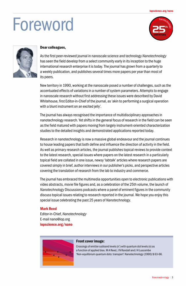
Dear colleagues,
As the first peer-reviewed journal in nanoscale science and technology Nanotechnology has seen the field develop from a select community early in its inception to the huge international research enterprise it is today. The journal has grown from a quarterly to a weekly publication, and publishes several times more papers per year than most of its peers.
New territory in 1990, working at the nanoscale posed a number of challenges, such as the accentuated effects of variations in a number of system parameters. Attempts to engage in nanoscale research without first addressing these issues were described by David Whitehouse, first Editor-in-Chief of the journal, as ‘akin to performing a surgical operation with a blunt instrument on an excited jelly’.
The journal has always recognised the importance of multidisciplinary approaches in nanotechnology research. Yet shifts in the general focus of research in the field can be seen as the field matured with papers moving from largely instrument-oriented characterization studies to the detailed insights and demonstrated applications reported today.
Research in nanotechnology is now a massive global endeavour and the journal continues to house leading papers that both define and influence the direction of activity in the field. As well as primary research articles, the journal publishes topical reviews to provide context to the latest research, special issues where papers on the latest research in a particularly topical field are collated in one issue, newsy ‘labtalk’ articles where research papers are covered simply in brief, author interviews in our publisher’s picks, and perspective articles covering the translation of research from the lab to industry and commerce.
The journal has embraced the multimedia opportunities open to electronic publications with video abstracts, movie file figures and, as a celebration of the 25th volume, the launch of Nanotechnology Discussions podcasts where a panel of eminent figures in the community discuss topical issues relating to research reported in the journal. We hope you enjoy this special issue celebrating the past 25 years of Nanotechnology.
Mark Reed Editor-in-Chief, Nanotechnology E-mail [email protected] iopscience.org/nano
Front cover image:Crossings of emitter subband levels (n’) with quantum dot levels (n) as a function of applied bias. M A Reed, J N Randall and J H Luscombe ‘Non-equilibrium quantum dots: transport’ Nanotechnology (1990) 1 63-66.
Forewordanniversary
Nanotechnology

4 Nanotechnology
iopscience.org/nano
Materials Science
Subscribe (free) to:Material Matters™aldrich.com/mm
Materials Driving InnovationFrom Aldrich® Materials Science
Materials Fabrication • Precursors for Nanomaterials and Nanocomposites; Monomers;
Deposition Precursors for PVD, CVD and Sputtering
Electronics• Nanowires, Printed Electronics Inks & Pastes; Materials for OPV,
OFET, OLED; Nanodispersions; CNTs & Graphene
Biomedical• Materials for Bone and Tissue Engineering: Nanoclays, PEGs,
Biodegradable & Natural Polymers; Functionalized Nanoparticles, Block Copolymers, & Dendrimers
©2013 Sigma-Aldrich Co. LLC. All rights reserved. Aldrich and Sigma-Aldrich are registered trademarks of Sigma-Aldrich Co. LLC, registered in the US and other countries.
aldrich.com/matsci
Materials Science
TM
Volume 7, Number 3
Targeting a better quality of life
Innovative Polymers Engineered for Drug Delivery and Tissue Engineering
Biodegradable Polyester-based Nanoparticle Formation by Miniemulsion Technique
Versatile Cell Culture Scaff olds via Bio-orthogonal Click Reactions
Chitosan-based Biomaterials
Biocompatible Dendritic Building Blocks for Advanced Biomedical Research
79073_MM7-3_US_r6.indd a 8/6/2012 9:39:15 AM
812761103
Gold Nanoparticle Dispersions
81276 Nanotechnology Ad_ 170mmx260mm_2.indd 1 10/1/2013 12:04:30 PM
Nanotechnology 5
iopscience.org/nano
ContentsBiology and medicine 6 Jeff Karp
Interview with 7 Miguel Jose Yacaman
Interview with 7 Tom Webster
Electronics and photonics 8 Meyya Meyyappan
Interview with 9 Craig Lent
Interview with 9 Stuart Lindsay
Energy at the nanoscale 10 Gary Brudvig
Interview with 11 Vladimir Dyakonov
Interview with 11 Silke Christiansen
Patterning and nanofabrication 12 S Mark Spearing
Interview with 13 Markku Leskelä
Interview with 13 Joachim P Spatz
Nanotechnology Timeline 14–19
Sensing and actuating 20 Jurgen Brugger
Interview with 21 Hans Peter Lang
Interview with 21 Xiao Wei Sun, Lionel Vayssieres and Yi Yang
Materials: synthesis or self-assembly 22 Stanislaus Wong
Interview with 23 Darrell H Reneker
Interview with 23 Maximilian Fichter
Materials: properties, characterization or tools 24 Mervyn Miles
Interview with 25 Hans-Jürgen Butt
Interview with 25 Anthony Guiseppi-Elie
Editorial Board 26
Journal team 27
Materials Science
Subscribe (free) to:Material Matters™aldrich.com/mm
Materials Driving InnovationFrom Aldrich® Materials Science
Materials Fabrication • Precursors for Nanomaterials and Nanocomposites; Monomers;
Deposition Precursors for PVD, CVD and Sputtering
Electronics• Nanowires, Printed Electronics Inks & Pastes; Materials for OPV,
OFET, OLED; Nanodispersions; CNTs & Graphene
Biomedical• Materials for Bone and Tissue Engineering: Nanoclays, PEGs,
Biodegradable & Natural Polymers; Functionalized Nanoparticles, Block Copolymers, & Dendrimers
©2013 Sigma-Aldrich Co. LLC. All rights reserved. Aldrich and Sigma-Aldrich are registered trademarks of Sigma-Aldrich Co. LLC, registered in the US and other countries.
aldrich.com/matsci
Materials Science
TM
Volume 7, Number 3
Targeting a better quality of life
Innovative Polymers Engineered for Drug Delivery and Tissue Engineering
Biodegradable Polyester-based Nanoparticle Formation by Miniemulsion Technique
Versatile Cell Culture Scaff olds via Bio-orthogonal Click Reactions
Chitosan-based Biomaterials
Biocompatible Dendritic Building Blocks for Advanced Biomedical Research
79073_MM7-3_US_r6.indd a 8/6/2012 9:39:15 AM
812761103
Gold Nanoparticle Dispersions
81276 Nanotechnology Ad_ 170mmx260mm_2.indd 1 10/1/2013 12:04:30 PM
DiD You KnoW? DiD You KnoW?
Look out for the publication of the Nanotechnology 25th Volume Special Issue in January 2014.
Nanotechnology now has a YouTube channel at youtube.com/nanotechnologyvideo
6 Nanotechnology
iopscience.org/nano
Ever since Louis Pasteur publicised his theory of germ-mediated putrefaction in the mid-nineteenth century there has been a growing preoccupation with developing more effective antiseptic agents. The increasing focus on nanostructures highlighted a possible potential to use metal nanoparticles as antibacterial agents. However, as Miguel Jose Yacaman points out, it was not clear what mechanism was behind their apparent antibacterial activity. In 2005 he and colleagues in Mexico and Texas in the US published a Nanotechnology article on studies using high angle annular dark field (HAADF) scanning transmission electron microscopy to investigate the effect of silver nanoparticles in the range of 1–100 nm on Gram-negative bacteria. “The main contribution of the paper was to really understand the role of the nanoparticles,” suggests Yacaman, “Not only in emitting ions, but also in attaching to the surface of the cells and the surface of the particles of bacteria.” The paper inspired considerable research activity in the field, and silver-nanoparticle-functionalized implants are now being explored in clinic trials.
While such studies focused on destroying bacterial cells, others investigated the potential use of nanostructures to promote mammalian cell proliferation on implants. Thomas J Webster and colleagues at Purdue University in the US emphasise how the molecular building blocks of life have unique properties determined by size, folding and patterns at the nanoscale. “It is because of this that it stands to reason that bone and neural cells are naturally accustomed to interacting with surfaces with a large degree of nanometre roughness.” Their 2003 article in Nanotechnology investigated the possible advantages of using nanostructures, in particular carbon nanofibres, as either neural or orthopaedic prosthetic devices. The research highlighted the improved cellular response on account of the nanoscale roughness of these components compared with traditional implants, which have microscale structuring but are smooth on the nanoscale.
Nanotechnology has come to represent the convergence of multiple disciplines including materials science, physics, chemistry, and biology. The field has been growing exponentially and there are now dozens of products on the market that harness the unique properties of nanomaterials to solve human problems.
The comparable dimensions of nanostructures and biological tissue features have a number of implications in medicine. By the end of the 1990s nanostructures were already revealing their huge potential in this area and work since has led to considerable progress in a range of areas including imaging, DNA sequencing, cancer diagnosis and treatment, and antibacterial agents.
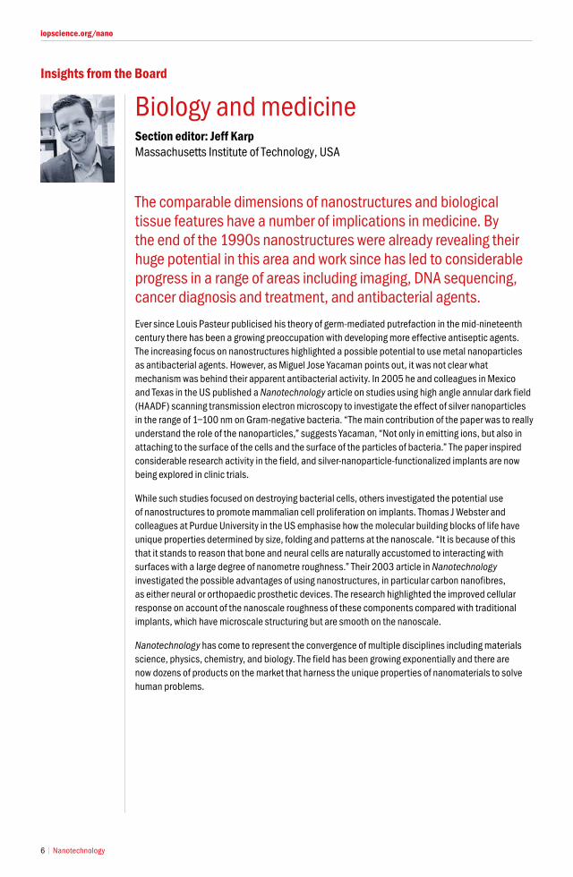
Biology and medicineinsights from the Board
Section editor: Jeff KarpMassachusetts Institute of Technology, USA
Nanotechnology 7
iopscience.org/nano
interviews with...
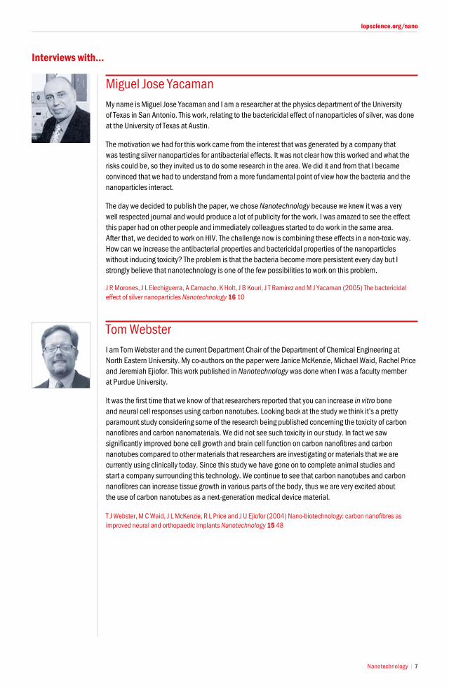
Miguel Jose Yacaman My name is Miguel Jose Yacaman and I am a researcher at the physics department of the University of Texas in San Antonio. This work, relating to the bactericidal effect of nanoparticles of silver, was done at the University of Texas at Austin.
The motivation we had for this work came from the interest that was generated by a company that was testing silver nanoparticles for antibacterial effects. It was not clear how this worked and what the risks could be, so they invited us to do some research in the area. We did it and from that I became convinced that we had to understand from a more fundamental point of view how the bacteria and the nanoparticles interact.
The day we decided to publish the paper, we chose Nanotechnology because we knew it was a very well respected journal and would produce a lot of publicity for the work. I was amazed to see the effect this paper had on other people and immediately colleagues started to do work in the same area. After that, we decided to work on HIV. The challenge now is combining these effects in a non-toxic way. How can we increase the antibacterial properties and bactericidal properties of the nanoparticles without inducing toxicity? The problem is that the bacteria become more persistent every day but I strongly believe that nanotechnology is one of the few possibilities to work on this problem.
J R Morones, J L Elechiguerra, A Camacho, K Holt, J B Kouri, J T Ramírez and M J Yacaman (2005) The bactericidal effect of silver nanoparticles Nanotechnology 16 10
Tom WebsterI am Tom Webster and the current Department Chair of the Department of Chemical Engineering at North Eastern University. My co-authors on the paper were Janice McKenzie, Michael Waid, Rachel Price and Jeremiah Ejiofor. This work published in Nanotechnology was done when I was a faculty member at Purdue University.
It was the first time that we know of that researchers reported that you can increase in vitro bone and neural cell responses using carbon nanotubes. Looking back at the study we think it’s a pretty paramount study considering some of the research being published concerning the toxicity of carbon nanofibres and carbon nanomaterials. We did not see such toxicity in our study. In fact we saw significantly improved bone cell growth and brain cell function on carbon nanofibres and carbon nanotubes compared to other materials that researchers are investigating or materials that we are currently using clinically today. Since this study we have gone on to complete animal studies and start a company surrounding this technology. We continue to see that carbon nanotubes and carbon nanofibres can increase tissue growth in various parts of the body, thus we are very excited about the use of carbon nanotubes as a next-generation medical device material.
T J Webster, M C Waid, J L McKenzie, R L Price and J U Ejiofor (2004) Nano-biotechnology: carbon nanofibres as improved neural and orthopaedic implants Nanotechnology 15 48
8 Nanotechnology
iopscience.org/nano
Of the many challenges in shrinking electronic devices to the nanoscale the issue of contacts has been among the most persistent. As Stuart Lindsay at Arizona State University points out, “Much of the confusion over ‘molecular electronics’ comes from ignoring the all-important contacts.” In 2001 he and colleagues at Arizona State University published a report characterizing the electrical contacts between a metal probe and molecular monolayers. As in so many areas of nanotechnology the research into scanning probe techniques that were first used for imaging nanoscale structures provided some useful tools for nanoelectronics studies. Lindsay and colleagues used a conducting atomic force microscope to obtain reversible current–voltage data and probe the nature of the contacts.
While the ceaseless miniaturization of electronics has been impressive in itself, the eccentricities of electronic behaviour in nanoscale structures have inspired new paradigms for circuits and computing. Locally-interconnected architectures such as cellular automata and cellular neural networks attracted significant research interest as a platform for exploiting quantum behaviour to reach beyond the capabilities of conventional electronics, as described in a 1993 report in the journal by Craig S Lent, P Douglas Tougaw, Wolfgang Porod and Gary H Bernstein at the University of Notre Dame. They showed that AND gates, OR gates, and inverters can be constructed and interconnected using coupled two-electron quantum dots. “Since the paper appeared, there has been a lot of inter-est and follow-on work, both by the Notre Dame group and others,” explains Lent. “I think we’re just scratching the surface of how to reconceive computer architecture using this post-transistor device.”
The fascinating details of the fundamental physics and mechanisms revealed in nanoscale systems were already enough to steal the attention of the scientifically oriented and curious. In addition, the vast assortment of keyring-sized convenience and entertainment gadgets often appended to mobile phones has popularised a level of interest in nanoscale research to the masses. The field of nanoelectronics research is ripe with new developments, and with the appetite aroused in electronics consumers, researchers in the field are no longer the only ones eagerly watching this space.
Electronics is one of the areas where the impact of advances in nanotechnology research on mainstream culture has been greatest. Anyone in possession of a mobile phone and familiar with the images of wall-sized computers from the 1960s will have a tangible sense of Moore’s Law, and how the number of transistors that fit on a chip has increased exponentially over the past few decades.
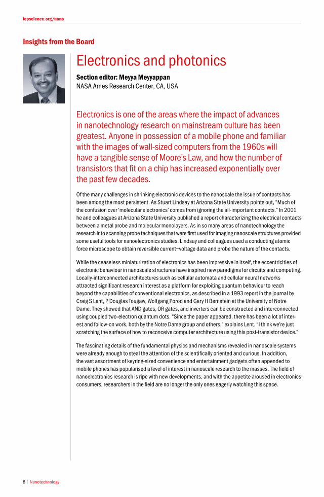
Electronics and photonicsinsights from the Board
Section editor: Meyya MeyyappanNASA Ames Research Center, CA, USA

Nanotechnology 9
iopscience.org/nano
interviews with...
Craig LentI’m Craig Lent, a Professor of Electrical Engineering, at the University of Notre Dame. My colleagues on the paper were Wolfgang Porod and Gary Bernstein, also professors in the Electrical Engineering Department.
In the very early days of nanoscience, Rolf Landauer made the point that interference-based quantum devices were unlikely to be robust. In a talk at one of the early nanoscience conferences, he said that what was really required was a bistable saturating response. We were convinced by his argument, and were on the look-out for such a characteristic. While doing some calculations on the basics of Coulomb blockade theory, I realized that the two-electron non-linear response I was seeing there was just what was needed. It could be adapted to a quantum-dot situation and be the basis of a new kind of device—the Quantum dot Cellular Automata (QCA) cell. By placing cells near each other, one could construct useful circuits.
Since the paper appeared, there has been a lot of interest and follow-on work, both by the Notre Dame group and others. QCA cells have been implemented with small metal islands, patterned semicon-ductor dots in GaAs and silicon, and in nanomagnets. Robert Wolkow’s group even made a QCA cell from individual dangling bonds on a silicon surface using a scanning tunneling microscope tip.
The question of how to think about QCA circuit design and circuit architecture has produced a lot of interesting subsequent work by Peter Kogge and Mike Niemier at Notre Dame, and many other groups around the world. I think we’re just scratching the surface of how to reconceive computer architecture using this post-transistor device.
C S Lent, P D Tougaw, W Porod and G H Bernstein (1993) Quantum cellular automata Nanotechnology 4 49
Stuart LindsayI am Stuart Lindsay, a Professor of Physics and Chemistry at Arizona State University and I direct the Center for Single Molecule Biophysics in the Biodesign Institute at Arizona State University. I was lucky to be around Paul Hansma’s lab in the very early days of scanning probe microscopy. The excitement was palpable and hasn’t really stopped.
The paper is about how one makes contacts to molecules to make electronic measurements. Much of the confusion over “molecular electronics” comes from ignoring the all-important contacts. A comprehensive treatment of this problem published by us in Science has now been cited well over 1000 times, so I think the message is now out there.
Since contacts are everything, we finally realized that we needed to develop universal “chemical fingers” for holding molecules on to electrodes. This led to the development of a technique we call recognition tunneling, currently licensed to Roche for DNA sequencing.
X D Cui, X Zarate, J Tomfohr, O F Sankey, A Primak, A L Moore, T A Moore, D Gust, G Harris and S M Lindsay (2002) Making electrical contacts to molecular monolayers Nanotechnology 13 5
10 Nanotechnology
iopscience.org/nano
Photovoltaics is indisputably among the dominating technologies in energy research. Organic photovoltaic (OPV) systems in particular have attracted huge interest on account of the flexible, light-weight, large-area and low-cost devices they promise. Poly(3-hexylthiphene) (P3HT) has good stability, as well as hole and field-effect mobility and has hence been a popular material in OPV research, often in conjunction with the fullerene derivative [6,6]-phenyl-C61 butyric acid methyl ester (PCBM). However as Vladimir Dyakonov, a professor of experimental physics at the University of Würzburg, Germany, points out, “Solid blends of semiconducting polymers and fullerenes sound easy, but they are not easy at all and till now remain one of the hardest OPV issues in terms of control.” In 2003 in Nanotechnology along with colleagues at the University of Oldenburg and the University of Groningen in The Netherlands, he reported a systematic study of thermally annealing P3HT:PCBM devices and determined the factors and mechanisms contributing to the energy conversion efficiency of the device.
Silicon — an element and an industry in its own right — has naturally inspired investigations in relation to photovoltaic applications. Arrays of silicon nanowires showed promise for potential thin-film solar-cell devices, but in 2008 research on silicon nanowire-based solar cells was still in its infancy, as Silke Christiansen and colleagues at the Institute of Photonic Technology and the Max Planck Institute of Microstructure Physics in Germany stated in their Nanotechnology paper. They went on to explain how silicon nanowires can be grown by a vapour-liquid-solid method on silicon wafers. They also described the unique optical properties of the nanowires and how they behave as solar cells.
The evident scope for exploiting nanostructures in energy applications prompted the introduction of a new ‘Energy section’ in Nanotechnology in 2011. Since then the section has attracted papers on the experimental and fundamental aspects of the physics related to a range of technologies including photovoltaics, batteries, fuel cells and hydrogen storage. If coal was black gold in the twentieth century, it seems the twenty-first equivalent will be nanotechnology.
With energy issues attracting mounting concern, research activity into alternatives to fossil fuels has soared over the past decade. As catalysts, electrodes and photovoltaic systems, the inherent properties of nanoscale structures have proved invaluable for optimising the efficiency of these new technologies
Energy at the nanoscaleinsights from the Board
Section editor: Gary Brudvig Yale University, New Haven, CT, USA
Nanotechnology 11
iopscience.org/nano
interviews with...
Vladimir DyakonovI am Vladimir Dyakonov, a Professor of Experimental Physics at the University of Würzburg, Germany. At the time the Nanotechnology paper was published I was doing research at the University of Oldenburg closely collaborating with the solar cell group of Professor Jürgen Parisi. Oldenburg is quite close to the University of Groningen, where “Mr PCBM” Professor Kees Hummelen was working and who provided us with his “magic” fullerenes, which still remain the best performing acceptors in polymer solar cells. Dana Chirvase, a PhD student, did an excellent job in the lab making devices.
Solid blends of semiconducting polymers and fullerenes sound easy, but they are not easy at all and remain one of the least controllable OPV issues. We decided to monitor the morphology by varying several parameters in a systematic way, i.e. by changing the fullerene load, processing temperature and seeing what the device performance will be. The result was the optimal recipe to make solar cells with the polymer P3HT and PCBM. A good resonance in the community, displayed by more than 40 citations a year, shows these results have some practical relevance for other groups.
OPV remains one of the most exciting interdisciplinary research fields. The record efficiency is now above 10%. Although the best solar cells are not built with the polymers we investigated that time, the ideas and concepts remain the same.
D Chirvase, J Parisi, J C Hummelen and V Dyakonov (2004) Influence of nanomorphology on the photovoltaic action of polymer–fullerene composites Nanotechnology 15 1317
Silke ChristiansenThe work was done at the Institute of Photonic Technology, Jena, Germany. I now lead the Institute for ‘Nano-architectures for Energy Conversion’ at the Helmholtz Center for Materials and Energy, Berlin as well as a Scientific Research and Technology Development Unit for ‘Photonic Nanostructures’ at the Max Planck Institute for the Science of Light (MPL) in Erlangen, Germany.
When our paper was published, vapour-liquid-solid (VLS) growth of nanowires was a topic of increasing scientific activity but only a few papers dealing with device integration of these nanowires were published. Devices of these early days of nanowire research were more concerned with biological sensing than showing minority carrier devices such as solar cells based on nanowires. As such, our paper was one of the first ones showing an admittedly lousy efficiency (<<1%). Still, we dared to publish an activity which serves now as a reference from the early days.
After the Nanotechnology article we realized that prior to showing good solar cell activities we needed to improve our understanding of electrical, optical and structural properties of the material and needed to develop proper technologies for device integration that permit reliable device designs with nanowires.
Meanwhile, the field has moved quickly and decent efficiencies (>10%) have been published and realized in our group as in many other groups active in this solar energy conversion field.
Th Stelzner, M Pietsch, G Andrä, F Falk, E Ose and S Christiansen (2008) Silicon nanowire-based solar cells Nanotechnology 19 295203
12 Nanotechnology
iopscience.org/nano
In fact while many new approaches have been developed, a number of the nanofabrication methods that have come to be widely used were derived or adapted from existing techniques for macroscale systems. One example is atomic layer deposition (ALD), or atomic layer epitaxy as it was referred to in the 1990s. Markku Leskelä and Mikko Ritala at the University of Helsinki in 1998 were among the first to consider the relevance of the approach for nanostructures. As they explain, “In the 1990s nanotechnology was quite a new area and no one had discussed the connection between ALD and nanotechnology.” Now ALD is widely used to deposit thin films on nanomaterials and tune their properties for a range of nanoelectronic and device structures. Look out for the special issue on atomic layer deposition in Nanotechnology later this year.
Today patterning and fabrication at the nanoscale remains a challenge and added to the question “how can certain structures be fabricated?” is the qualifier “and how economically?” Transferring technology from the lab to industry requires cheap, reproducible high throughput techniques. At the same time many applications require high-quality and precision structures in order to work effectively. As Roman Glass, Martin Möller and Joachim P Spatz in Germany pointed out in an article in Nanotechnology ten years ago, “Principally, there are two major directions scientists follow to address demands from proposed applications in nanosciences, the so-called top-down approach and bottom-up approach.” The choice between top-down and bottom-up approaches is based on considerations of unit cost, required throughput and repeatability, and desired precision. Glass and co-workers go on to describe a patterning technique that maximises the benefits of both approaches, that is, block copolymer micelle nanolithography. By pre-patterning a structure using traditional photo or e-beam lithography, followed by self-assembly directed by the pre-pattern, the fabrication of a number of features can be achieved.
The degree of control over nanoscale systems today highlights how far the field has come over the past 25 years. And with the powerful partnership of innovation and recycling of existing technology, we can expect some exceptional capabilities to be available in the years to come.
Any research and application of nanotechnology assumes that the necessary structures can be made. In 1990 when Nanotechnology was launched, this prerequisite was far from trivial—only a few structures had actually been demonstrated as feasible. The extreme precision required was a huge challenge in itself, and in addition studies of nanoscale structures were full of surprises. Legitimate assumptions as to what existing technologies could be successfully applied at such diminished scales were few and far between.
Patterning and nanofabricationinsights from the Board
Section editor: S Mark Spearing University of Southampton, UK
Nanotechnology 13
iopscience.org/nano
interviews with...
Markku Leskelä I am Markku Leskelä, a Professor of Inorganic Chemistry at University of Helsinki. I started atomic layer deposition (ALD) (that time called atomic layer epitaxy) related studies in 1980. The ALD studies were focused on films needed in electroluminescent displays which were the only commercial applications of ALD in the 1980s. In 1990 I started ALD research with Mikko Ritala at University of Helsinki, with a broad focus on the basic process development including precursor synthesis and reaction mechanism studies and looking at possibilities of ALD in various fields. During the 1990s it became clear that ALD was needed in microelectronics and also that our research was focused for high dielectric constant oxides, metal and barrier films. From the very beginning of the emergence of nanotechnology in its various forms it was obvious to us that ALD had a lot to contribute there too, as has then been realized by us and many others.
We described in the paper the basic properties of ALD and showed how very thin films had been deposited on different substrates. We also discussed the nanolaminate concept we had introduced a few years earlier. In outlook we speculated the suitability of ALD to nanotechnology. In the 1990s nanotechnology was quite a new area and no one had discussed the connection between ALD and nanotechnology. In that sense the paper was visionary.
ALD enables the deposition of thin conformal films in a controlled way on substrates of any size and shape. Now it is clear that ALD is a very suitable tool for growing films on nanomaterials and tuning their properties. Our review can be considered as a trigger for this field.
M Ritala and M Leskelä (1999) Atomic layer epitaxy - a valuable tool for nanotechnology? Nanotechnology 10 19
Joachim P Spatz I am Joachim P Spatz, a materials scientist and biophysicist. I joined the Max Planck Institute for Intelligent Systems as a Director for the Department of New Materials and Biosystems in 2004. I am also a Full Professor at the University of Heidelberg and Head of the Department of Biophysical Chemistry.
We started to look into the field of block copolymer nanolithography in order to generate nano-patterns by self-assembly at a length scale which is close to the molecular scale. The original purpose of such patterns was for directing locations of different molecules which would not be possible by other means. Finally, we strongly immersed ourselves into biofunctionalisation strategies for directing cell adhesion at length scales of single transmembrane receptors.
My paper describes the progress and the practical application of micellar diblock copolymer lithography. The information in the paper is useful for different fields of applications, including chemistry, physics and biology.
We applied the basis of micellar diblock copolymer lithography to different applications in optics (antireflection coatings), biology (cell adhesion and migration) and lithography in general. The work was extended to different materials which find application in heterogeneous catalysis.
R Glass, M Möller and J P Spatz (2003) Block copolymer micelle nanolithography Nanotechnology 14 1153
The interviews detailed in this brochure highlight the significant impact of papers published in Nanotechnology and the considerable role that they have played in steering future research.
This foldout provides an overview of some of those important advances and themes in developing technologies at the nanoscale.
Nanotechnology began in the advancing stages of the field 25 years ago and we are proud to remain at the forefront. Our articles are of the highest quality and they are downloaded in their millions by readers worldwide. The next 25 years are sure to be progressive and we look forward to playing a role in those future developments.
iopscience.org/nano
open

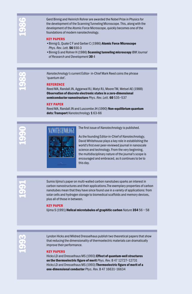
1986
Gerd Binnig and Heinrich Rohrer are awarded the Nobel Prize in Physics for the development of the Scanning Tunneling Microscope. This, along with the development of the Atomic Force Microscope, quickly becomes one of the foundations of modern nanotechnology.
KEY PAPERS• Binnig G, Quate C F and Gerber C (1986) Atomic Force Microscope
Phys. Rev. Lett. 56 930-3• Binnig G and Rohrer H (1986) Scanning tunneling microscopy IBM Journal
of Research and Development 30 4
1988
Nanotechnology’s current Editor- in-Chief Mark Reed coins the phrase ‘quantum dot’.
REFEREnCEReed MA, Randall JN, Aggarwal RJ, Matyi RJ, Moore TM, Wetsel AE (1988) observation of discrete electronic states in a zero-dimensional semiconductor nanostructure Phys. Rev. Lett. 60 535–537
KEY PAPERReed MA, Randall JN and Luscombe JH (1990) non-equilibrium quantum dots: Transport Nanotechnology 1 63-66
1990
The first issue of Nanotechnology is published.
As the founding Editor-in-Chief of Nanotechnology, David Whitehouse plays a key role in establishing the world’s first ever peer-reviewed journal in nanoscale science and technology. From the very beginning, the multidisciplinary nature of the journal’s scope is encouraged and embraced, as it continues to be to this day.
1991
Sumio Iijima’s paper on multi-walled carbon nanotubes sparks an interest in carbon nanostructures and their applications.The exemplary properties of carbon nanotubes mean that they have since found use in a variety of applications: from solar cells and hydrogen storage to biomedical scaffolds and memory devices, plus all of those in between.
KEY PAPERIijima S (1991) Helical microtubules of graphitic carbon Nature 354 56 – 58
1993
Lyndon Hicks and Mildred Dresselhaus publish two theoretical papers that show that reducing the dimensionality of thermoelectric materials can dramatically improve their performance.
KEY PAPERSHicks LD and Dresselhaus MS (1993) Effect of quantum-well structures on the thermoelectric figure of merit Phys. Rev. B 47 12727–12731Hicks LD and Dresselhaus MS (1993) Thermoelectric figure of merit of a one-dimensional conductor Phys. Rev. B 47 16631–16634
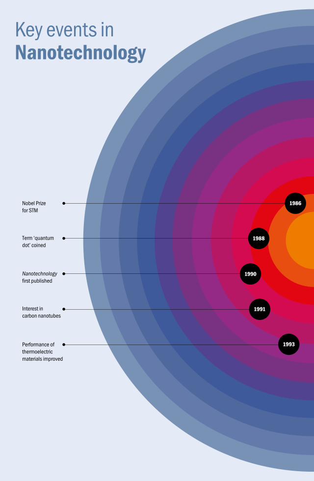
Term ‘quantum dot’ coined
Nobel Prize for STM
Performance of thermoelectric materials improved
Interest in carbon nanotubes
Nanotechnology first published
1986
1988
1990
1991
1993
Key events in nanotechnology
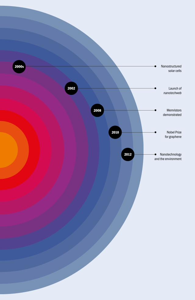
Nanostructured solar cells
Launch of nanotechweb
Memristors demonstrated
Nobel Prize for graphene
Nanotechnology and the environment
2000s
2002
2008
2010
2012
2008
Stanley Williams’ group at HP Labs finds that Chua’s ‘lost circuit element’, the memristor, can be demonstrated with nanoscale systems.
REFEREnCEDmitri B. Strukov, Gregory S. Snider, Duncan R. Stewart & R. Stanley Williams (2008) The missing memristor found Nature 453 80-83
KEY PAPERS• Chua LO (1971) Memristor-The Missing Circuit Element IEEE Trans. on
Circuit Theory 18 (5) 507-519• Di Ventra M and Pershin YV (2013) on the physical properties of memristive,
memcapacitive and meminductive systems Nanotechnology 24 255201
2010
The Nobel Prize in Physics is awarded to Andre Geim and Konstantin Novoselov for their work on graphene.
KEY PAPERSNovoselov KS, Geim AK., Morozov SV, Jiang D., Zhang Y, Dubonos SV, Grigorieva IV, Firsov AA (2004) Electric field in atomically thin carbon films Science 306 666-669
2012
The impact of nanotechnology on the environment continues to be of concern. Nanotechnology published a special issue highlighting green synthesis methods and more sustainable nanotechnologies.
nanotechnology Volume 23 number 29 ‘Green nanotechnology’
The next decade sees nanostructures being increasingly incorporated into solar cells. Neil C Greenham and Michael Grätzel are guest editors for:
nanotechnology Volume 19 number 42 ‘nanostructured solar cells’
2000
s20
02 Nanotechweb.org is launched to provide a ‘go to’ place for the nanotechnology community. Providing news, an events calendar, product information, jobs and a free weekly news alert highlighting key research worldwide, nanotechweb has become a key information source.
20 Nanotechnology
iopscience.org/nano
In fact the work on scanning probe techniques that had first brought nanostructures into view in itself led to some powerful sensing technologies. The ability to monitor cantilever deflections with an accuracy of 0.1 nm lent these systems to highly sensitive protein detection applications. Then extending the technique from single cantilevers to arrays allowed the technology to be scaled up without loss of sensitivity as Ch Gerber, Hans Peter Lang and colleagues demonstrated in their 2003 paper in Nanotechnology. “The paper reports on our first observation of protein detection using cantilever array sensors,” explains Lang. “This was our first collaboration with a hospital and our first application of the sensors in the medical field.” Lang and colleagues demonstrated continuous label-free detection of two cardiac biomarker proteins (creatin kinase and myoglobin) at concentrations below 20 μg ml−1 using an array of microfabricated cantilevers functionalized with covalently anchored anti-creatin kinase and anti-myoglobin antibodies.
Zinc oxide has been one of the most popular materials in nanotechnology research for the past two decades. The electronic properties of ZnO nanostructures in particular have garnered high interest on account of the sensitivity to environmental aspects such as strain, and the presence of gas molecules. The work by Xiao Wei Sun and colleagues at Nanyang Technological University in Singapore and the National Institute for Materials Science reported in Nanotechnology in 2006 was an excellent example of how advances in fabrication techniques helped the development of ZnO devices with enhanced sensitivities. By using arrays of aligned ZnO nanowires instead of single or tangled structures they demonstrated a system with high sensitivity to H2, NH3 and CO and huge promise for large-scale fabrication of cost-effective and high performance gas sensors. “It is really amazing that we can make ZnO in nanowire form and greatly enhance its sensitivity as we showed in this paper,” adds Xiao Wei Sun.
Research at the nanoscale had initially focused on finding better ways to probe nanostructures, and in so doing revealed what remarkable tools nanostructures themselves provide for probing the environment around them. As nanofabrication capabilities and our understanding of the behaviour of these systems continue to increase, we can expect a great deal more from the fruitful symbiosis between nanotechnology and sensing applications.
The glint of potential applications has never been far from view in the study of nanostructures. The unusual properties revealed in nanosystems, that had tickled the collective curiosity of the fundamental research community, tugged at the imaginations of those who recognised the extraordinary device opportunities these structures presented, in particular in sensing.
Sensing and actuating insights from the Board
Section editor: Juergen Brugger Ecole Polytechnique Federale de Lausanne, Switzerland
Nanotechnology 21
iopscience.org/nano
interviews with...
Hans Peter LangI am Hans Peter Lang and I’m working at the Swiss Nanoscience Institute in Basel. Having studied the properties of nanomaterials, such as high temperature superconductors and various forms of carbon using STM and AFM, I worked on the use of AFM cantilevers as nanomechanical sensors for the detection of volatile molecules.
Back in 2003 we had just finished the development of cantilever array sensors for the detection of volatile compounds in gaseous environments and had applied the technique to the detection of biochemical reactions in liquids. After first success with hybridisation of DNA oligonucleotides, we started the detection of cardiac biomarker proteins for our Nanotechnology paper. The paper reports our first observation of protein detection using cantilever array sensors and our first collaboration with a hospital. We demonstrated the rapid detection of cardiac biomarkers within minutes which can be an essential advantage in comparison to classical antibody detection assays.
This article was the first in a series of papers in which the applicability of the cantilever array sensing technique was explored. Medical studies included the detection of biomarkers and efficiency testing of therapies, e.g for interferons as well as the applicability of a melanoma drug personalised medicine for patients with specific genetic mutation. Consequently, this article actually had a large impact on the development of our research.
Y Arntz, J D Seelig, H P Lang, J Zhang, P Hunziker, J P Ramseyer, E Meyer, M Hegner and Ch Gerber (2003) Label-free protein assay based on a nanomechanical cantilever array Nanotechnology 14 86
Xiao Wei Sun, Lionel Vayssieres and Yi Yang
We are Xiao Wei Sun, a Chair Professor in the Department of Electrical and Electronic Engineering at the South University of Science and Technology in Shenzhen; Lionel Vayssieres, Co-Director of the International Research Center for Renewable Energy, Xi’an Jiaotong University; and Yi Yang, a research scientist at Data Storage Institute, Singapore.
The work was done in 2006 after Lionel published the first paper on hydrothermally grown ZnO nanorods. At that time, we were interested in thin film forms of ZnO, but then we discovered Charles Lieber’s work on semiconducting nanowires and Peidong Yang’s work on ZnO nanowire lasing. We began working on ZnO nanowires/nanorods for device applications. While ZnO was already known as a gas sensor, the strategy of using aqueous-grown oriented nanorods was completely new for such an application. Room temperature operated sensors are of crucial importance for several sensitive applications as well as to reduce the overall cost of devices and our results showed unprecedented response and sensitivity at these temperatures.
The scientific community received this article very well and the ZnO gas sensor paper we reported here is just one example of quite a few highly cited papers. It is really amazing that we can make ZnO in nanowire form and greatly enhance its sensitivity as we showed in this paper. The success of this paper triggered a real interest in combining the output of fundamental academic research and engineering in joint collaborative work to create functioning nanodevices.
J X Wang, X W Sun, Y Yang, H Huang, Y C Lee, O K Tan and L Vayssieres (2006) Hydrothermally grown oriented ZnO nanorod arrays for gas sensing applications Nanotechnology 17 4995
22 Nanotechnology
iopscience.org/nano
Darrell H Reneker was one of the pioneers in the field who first popularised the term “electrospinning”. In 1996, he and colleague Iksoo Chun at the University of Akron published a paper in Nanotechnology describing the process and summarising related research reaching as far back as 1745. They reported nanofibers of more than 20 polymers, electrospun from polymer solutions and melts. The field continues to sustain a high level of research activity with over 5,000 research papers on nanofibers published in the past decade, and related applications including largely filtration and biological research.
Catalysis has emerged as an important if challenging field within nanotechnology. “The fact that solid state reactions between composite mixtures and hydrogen can be ‘catalysed’ by certain transition metal additives such as Ti compounds has been a mystery since their discovery in the late 1990s,” states Maximilian Fichtner, who has spent the past 12 years engaged in energy storage research. He and fellow researchers at the Karlsruhe research centre in Germany studied small Ti clusters as catalysts for hydrogenation of NaAlH4 for hydrogen storage. Their experiments published in the journal in 2003 indicated that the size of the Ti particles was crucial for the activity of the catalyst. “The paper had an impact not only on the H storage community where it motivated researchers to put more emphasis on the dispersion of transition metal additives,” explains Fichtner. ”But it was also cited by many other groups as an example for the potential power of a nanotechnological approach in practical applications.”
Over the decades, materials synthesis has evolved from something akin to a randomized trial-and-error approach to a fundamentally more elegant and more rational, technical art. Nowadays a deeper mechanistic understanding of growth and formation guides the production of a range of materials with physical properties tailored to specific design applications. Exciting innovative developments in the field seem likely to persist, though the full potential of nanoscale systems can only be tapped when cost-effective, efficient, and scientifically valuable approaches for producing nanostructures of well-defined chemical composition and physical properties are discovered and put into good use.
Controlled efficient synthesis of nanomaterials has been the preoccupation of a generation of researchers since the first glimpse at the nanoscale in the 1980s. At first, very little was known about how materials behaved at this scale and the ability to generate systems reproducibly for further detailed characterization of their properties was a legitimate challenge.
Materials: synthesis or self-assemblyinsights from the Board
Section editor: Stanislaus Wong University of New York, NY, USA
Nanotechnology 23
iopscience.org/nano
interviews with...
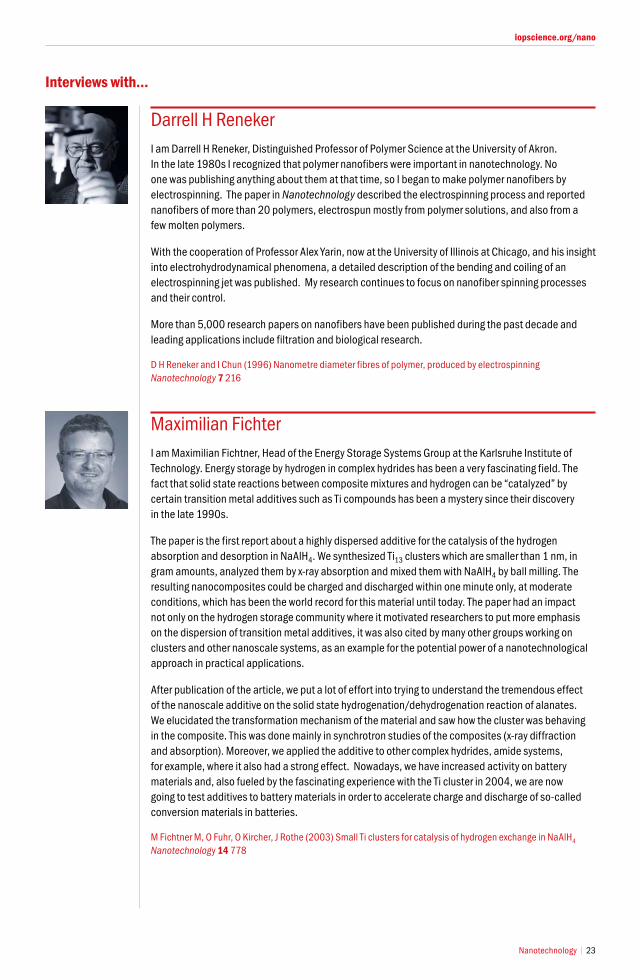
Darrell H RenekerI am Darrell H Reneker, Distinguished Professor of Polymer Science at the University of Akron. In the late 1980s I recognized that polymer nanofibers were important in nanotechnology. No one was publishing anything about them at that time, so I began to make polymer nanofibers by electrospinning. The paper in Nanotechnology described the electrospinning process and reported nanofibers of more than 20 polymers, electrospun mostly from polymer solutions, and also from a few molten polymers.
With the cooperation of Professor Alex Yarin, now at the University of Illinois at Chicago, and his insight into electrohydrodynamical phenomena, a detailed description of the bending and coiling of an electrospinning jet was published. My research continues to focus on nanofiber spinning processes and their control.
More than 5,000 research papers on nanofibers have been published during the past decade and leading applications include filtration and biological research.
D H Reneker and I Chun (1996) Nanometre diameter fibres of polymer, produced by electrospinning Nanotechnology 7 216
Maximilian FichterI am Maximilian Fichtner, Head of the Energy Storage Systems Group at the Karlsruhe Institute of Technology. Energy storage by hydrogen in complex hydrides has been a very fascinating field. The fact that solid state reactions between composite mixtures and hydrogen can be “catalyzed” by certain transition metal additives such as Ti compounds has been a mystery since their discovery in the late 1990s.
The paper is the first report about a highly dispersed additive for the catalysis of the hydrogen absorption and desorption in NaAlH4. We synthesized Ti13 clusters which are smaller than 1 nm, in gram amounts, analyzed them by x-ray absorption and mixed them with NaAlH4 by ball milling. The resulting nanocomposites could be charged and discharged within one minute only, at moderate conditions, which has been the world record for this material until today. The paper had an impact not only on the hydrogen storage community where it motivated researchers to put more emphasis on the dispersion of transition metal additives, it was also cited by many other groups working on clusters and other nanoscale systems, as an example for the potential power of a nanotechnological approach in practical applications.
After publication of the article, we put a lot of effort into trying to understand the tremendous effect of the nanoscale additive on the solid state hydrogenation/dehydrogenation reaction of alanates. We elucidated the transformation mechanism of the material and saw how the cluster was behaving in the composite. This was done mainly in synchrotron studies of the composites (x-ray diffraction and absorption). Moreover, we applied the additive to other complex hydrides, amide systems, for example, where it also had a strong effect. Nowadays, we have increased activity on battery materials and, also fueled by the fascinating experience with the Ti cluster in 2004, we are now going to test additives to battery materials in order to accelerate charge and discharge of so-called conversion materials in batteries.
M Fichtner M, O Fuhr, O Kircher, J Rothe (2003) Small Ti clusters for catalysis of hydrogen exchange in NaAlH4 Nanotechnology 14 778
24 Nanotechnology
iopscience.org/nano
Being the first peer-reviewed journal devoted to research at this scale, Nanotechnology naturally attracted many of the papers that defined scanning probe research at the time, such as the work on atomic force microscopy by Hans-Jürgen Butt and Manfred Jaschke at the Max-Planck Insitut für Biophysik. In atomic force microscopy accurate knowledge of the cantilever spring constant was a crucial and, at the time, elusive parameter for implementing the technique effectively. In 1994 Butt and Jashcke reported calculations of the thermal noise in tip cantilevers, which is used to calibrate the spring constant, revealing that more than one vibration mode was involved. The work highlighted some restraints associated with using the optical lever technique to measure the cantilever deflection.
The first reports on the properties of materials structured at the nanoscale brimmed with surprises. In its nanomorphologies, carbon was promoted from soot to one of the most sought-after elements in materials research. Interest was first piqued with the discovery of “buckyballs” in 1985. While the isolation of graphene finally culminated in a Nobel Prize, it was perhaps carbon nanotubes, first reported in 1990, that triggered the initial gear change in research activity. Reports of their unique combination of mechanical, electronic and optical properties prompted some inspired innovations in both applied and fundamental research.
In 2002 Guiseppi-Elie and his colleagues in the US found that with the proximity that could be achieved through the nanoscale morphologies combined with their electrical properties, tunnelling could be achieved between carbon nanotubes and redox active enzymes. In these biomolecules the moieties of interest are deeply embedded within the molecular structure, so direct electrical communication had previously proved challenging. As the US researchers explained, “The combination of single-walled nanotubes with redox active enzymes would appear to offer an excellent and convenient platform for a fundamental understanding of biological redox reactions as well as the development of reagentless biosensors and nanobiosensors.” A huge amount of research activity in similar studies followed.
Carbon is quite an extreme example of how nanoscale morphologies have introduced exotic properties to some apparently familiar substances. New materials, phenomena and applications are constantly emerging, and 25 years on interest in the properties and tools associated with nanomaterials shows little sign of abating.
Scanning probe microscopy launched nanostructures into the limelight in the late 1980s. No surprise then that as the study of nanotechnology subsequently emerged as a field in its own right, a great deal of research activity was focused on further developing the tools that had first brought nanostructures into view.
Materials: properties, characterization or tools
insights from the Board
Section editor: Mervyn Miles University of Bristol
Nanotechnology 25
iopscience.org/nano
interviews with...
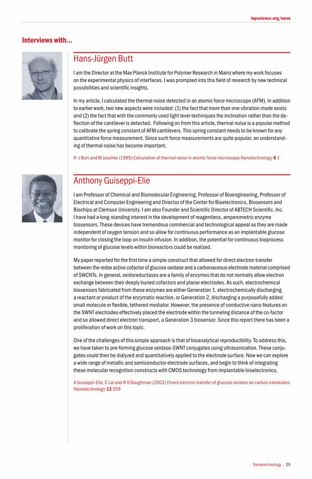
Hans-Jürgen Butt I am the Director at the Max Planck Institute for Polymer Research in Mainz where my work focuses on the experimental physics of interfaces. I was prompted into this field of research by new technical possibilities and scientific insights.
In my article, I calculated the thermal noise detected in an atomic force microscope (AFM). In addition to earlier work, two new aspects were included: (1) the fact that more than one vibration mode exists and (2) the fact that with the commonly used light lever techniques the inclination rather than the de-flection of the cantilever is detected. Following on from this article, thermal noise is a popular method to calibrate the spring constant of AFM cantilevers. This spring constant needs to be known for any quantitative force measurement. Since such force measurements are quite popular, an understand-ing of thermal noise has become important.
H -J Butt and M Jaschke (1995) Calculation of thermal noise in atomic force microscopy Nanotechnology 6 1
Anthony Guiseppi-ElieI am Professor of Chemical and Biomolecular Engineering, Professor of Bioengineering, Professor of Electrical and Computer Engineering and Director of the Center for Bioelectronics, Biosensors and Biochips at Clemson University. I am also Founder and Scientific Director of ABTECH Scientific, Inc.I have had a long-standing interest in the development of reagentless, amperometric enzyme biosensors. These devices have tremendous commercial and technological appeal as they are made independent of oxygen tension and so allow for continuous performance as an implantable glucose monitor for closing the loop on insulin infusion. In addition, the potential for continuous bioprocess monitoring of glucose levels within bioreactors could be realized.
My paper reported for the first time a simple construct that allowed for direct electron transfer between the redox active cofactor of glucose oxidase and a carbonaceous electrode material comprised of SWCNTs. In general, oxidoreductases are a family of enzymes that do not normally allow electron exchange between their deeply buried cofactors and planar electrodes. As such, electrochemical biosensors fabricated from these enzymes are either Generation 1, electrochemically discharging a reactant or product of the enzymatic reaction, or Generation 2, discharging a purposefully added small molecule or flexible, tethered mediator. However, the presence of conductive nano-features on the SWNT electrodes effectively placed the electrode within the tunneling distance of the co-factor and so allowed direct electron transport, a Generation 3 biosensor. Since this report there has been a proliferation of work on this topic.
One of the challenges of this simple approach is that of bioanalytical reproducibility. To address this, we have taken to pre-forming glucose oxidase-SWNT conjugates using ultrasonication. These conju-gates could then be dialyzed and quantitatively applied to the electrode surface. Now we can explore a wide range of metallic and semiconductor electrode surfaces, and begin to think of integrating these molecular recognition constructs with CMOS technology from implantable bioelectronics.
A Guiseppi-Elie, C Lei and R H Baughman (2002) Direct electron transfer of glucose oxidase on carbon nanotubes Nanotechnology 13 559
26 Nanotechnology
iopscience.org/nano
Editorial Board
Journal Team
Editor-in-ChiefMark Reed Yale University, New Haven, CT, USA
Section EditorsBiology and Medicine EditorJeffrey M Karp Massachusetts Institute of Technology, USA
Electronics and Photonics EditorMeyya Meyyappan NASA Ames Research Center, CA, USA
Energy at the Nanoscale EditorGary Brudvig Yale University, New Haven, CT, USA
Patterning and Nanofabrication EditorS Mark Spearing University of Southampton, UK
Sensing and Actuating EditorJürgen Brugger Ecole Polytechnique Federale de Lausanne, Switzerland
Materials: Synthesis or Self-Assembly EditorStanislaus Wong State University of New York, NY, USA
Materials: Properties, Characterization or Tools EditorMervyn J Miles University of Bristol
Editorial BoardYoshio Bando National Institute for Materials Science, Tsukuba, Japan Supriyo Bandyopadhyay Virginia Commonwealth University, USAKarl Berggren Massachusetts Institute of Technology, USAChristian Brosseau Université de Bretagne Occidentale, France Sarah Burke University of British Columbia, CanadaJamal Deen McMaster University, Hamilton, CanadaHongjin Fan Nanyang Technological University, SingaporeGeorge Grüner University of California, Los Angeles, USASeunghun Hong Seoul National University, South KoreaRu Huang Peking University, ChinaSergei Kalinin Oak Ridge National Laboratory, TN, USADae-Joon Kang Sungkyunkwan University, South Korea
Frederik Krebs Technical University of Denmark, DenmarkRay LaPierre McMaster University, Hamilton, CanadaTakhee Lee Seoul National University, South KoreaJan Linnros KTH Royal Institute of Technology, SwedenDan Peer Tel Aviv University, IsraelMichael Steigerwald Columbia University, NY, USAMahendra Sunkara University of Louisville, KY, USAJohn Vajo HRL Laboratories LLC, CA, USAGeorge M Whitesides Harvard University, Cambridge, MA, USAHui Yang Suzhou Institute, Jiangsu, ChinaChris Yip University of Toronto, CanadaWeian Zhao University of California, Irvine, USAChongWu Zhou University of Southern California, USA
Fabrice Baker-LivingstoneMarketing Executive
Rosalind BarrettPublishing Administrator
Simon BuckmasterPublishing Editor
Anna DemmingPublishing Editor
Paula KentProduction Editor
Chris ThomasGroup Advertising Manager
James TyrrellEditor, nanotechweb.org
Danny TurnerGroup Publishing
Administrator
Tim SmithSenior Publisher
Alex WotherspoonPublisher
Johnathon KeenPublishing Editor
Maggie SimmonsPublishing Editor
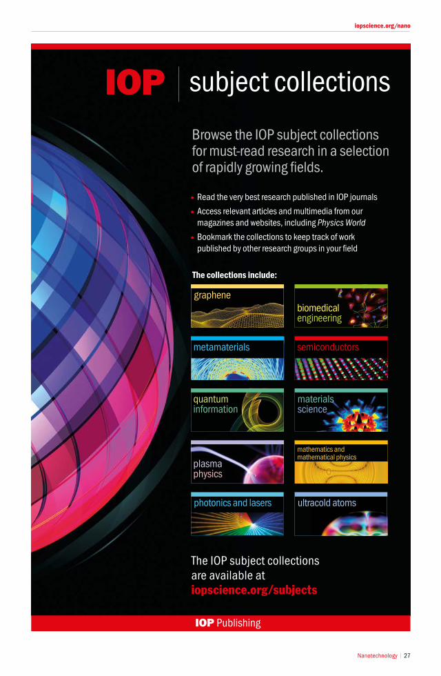
Nanotechnology 27
iopscience.org/nano
Browse the IOP subject collections for must-read research in a selection of rapidly growing fields.
• Read the very best research published in IOP journals
• Access relevant articles and multimedia from our magazines and websites, including Physics World
• Bookmark the collections to keep track of work published by other research groups in your field
The collections include:
The IOP subject collections are available at iopscience.org/subjects
subject collections IOP
biomedical engineering
quantum information
plasmaphysics
materials science
graphene
semiconductors
mathematics and mathematical physics
metamaterials
ultracold atomsphotonics and lasers
28 Nanotechnology
iopscience.org/nano
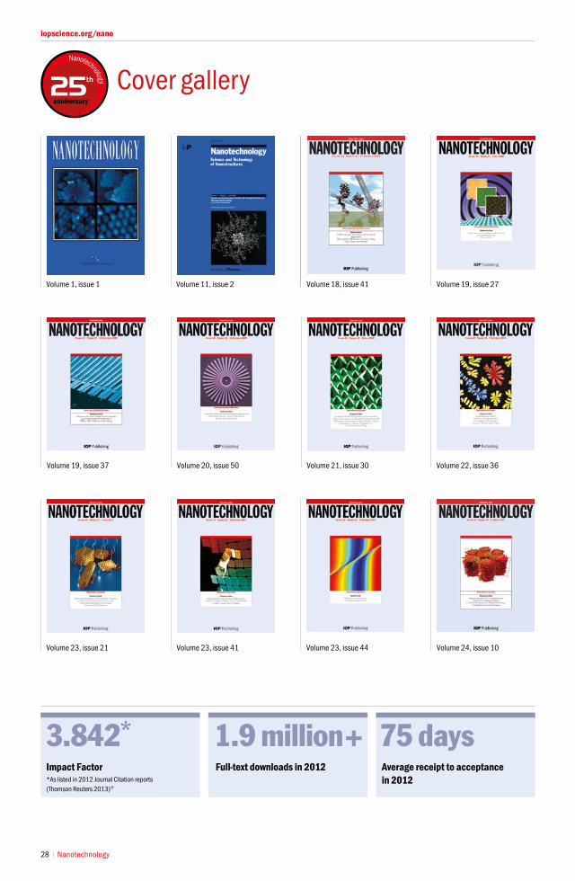
impact Factor *As listed in 2012 Journal Citation reports (Thomson Reuters 2013)®
75 days1.9 million +3.842*Average receipt to acceptance in 2012
Full-text downloads in 2012
Cover gallery
Volume 1, issue 1 Volume 11, issue 2 Volume 18, issue 41 Volume 19, issue 27
Volume 22, issue 36Volume 21, issue 30Volume 20, issue 50Volume 19, issue 37
Volume 24, issue 10Volume 23, issue 44Volume 23, issue 21 Volume 23, issue 41
anniversary
Nanotechnology
Nanotechnology 29
iopscience.org/nano
Why publish with Nanotechnology?
By publishing your paper with Nanotechnology you can take advantage of a number of other benefits including:
Do you want to know more?To find out more about publishing with Nanotechnology, please visit iopscience.org/nano or contact the journal team at [email protected].
1 HiGH iMPACTNanotechnology publishes a high volume of quality articles on a weekly basis. Despite this frequency, Nanotechnology has an impressive impact factor of 3.842, as listed by the ISI 2012 Science Citation Index Journal Citation Report.
2 FAST PuBLiCATionOur peer-review process is rigorous and efficient, with an average receipt to acceptance time of 75 days.
3 WoRK WiTH THE BEST in THE WoRLDNanotechnology features top research from institutions throughout the world; only around 20% of articles are accepted for publication.
And thAt’s not All…By publishing your paper with Nanotechnology you can take advantage of a number of other benefits including:
Prestige Nanotechnology was the first published journal dedicated solely to nanoscience and nanotechnology
nanotechweb.org Additional promotion opportunities are available on our sister website nanotechweb.org, which is viewed by more than 55 000 people per month.
Widely read More than 1.9 million Nanotechnology articles were downloaded in 2012.
Fantastic visibility and exposure The journal will be represented at more than 40 conferences in 2014.
open access The option to publish articles in open access format.
DiD You KnoW? DiD You KnoW?Nanotechnology now publishes podcasts. In celebration of our 25th volume, Professor Christoph Gerber, Professor James K Gimzewski, and Professor Franz Gießibl discuss the early days of nanotechnology, the state of the field currently and the future prospects.
Extended versions of these interviews and additional video content can be found at iopscience.org/nano-25
UHV
NANOPARTICLE
GENERATION
MOC.NOITISOPEDSITNAM.WWW
NON-THERMALDEPOSITIONPROCESS
CONTROL OF FILM STRUCTURE
FROM POROUS TO ADHERENTIMPLANTEDNANOPARTICLES
[email protected] FOLLOW US ON:
NEGATIVELY CHARGED
NANOCLUSTERS
PARTICLE SIZE
RANGE 1-20 NM
Characterize properties of nanoscale materials:
Carbon nanotubes
Graphene
Nanowires
NEMS
Nanomagnets
Spintronics
614.891.2243 | www.lakeshore.com
Advancing Nanomaterials
Probe Stations and Materials Characterization SystemsLake Shore systems provide the sensitivity and control needed for reliable measurement and characterization of nanomaterials.
Lake Shore’s cryogenic probe stations provide precisely controlled environments for non-destructive measurement of the electrical properties of materials and early-stage electronic devices.
Lake Shore's newest materials characterization system uses non-destructive, non-contact THz energy to measure important phenomena in novel electronic and magnetic materials.
Look to Lake Shore for the expertise and technology to support your work.
Cryogen & Cryogen-Free Probing
THz CharacterizationSystem
PMCMicroMag™
AGM/VSMsng™
Ms
[email protected] |+44 (0)1925 445 225
for further details of Hiden Analytical products contact:
www.HidenAnalytical.com
Instruments for Advanced Science
Thin FilmSurface Analysis
■ Static and dynamic SIMS ■ Chemical composition & depth
profi ling ■ SIMS for FIB including
bolt-on modules & integrated SIMS-on-a-Flange
■ Choice of primaryions
■ Complete SIMS workstations
Plasma Characterisation
■ EQP ion mass and energy analyser
■ RF, DC, ECR and pulsed plasma ■ Neutrals and neutral radicals ■ Time resolved analysis ■ HPR-60 extends
analyses to atmospheric pressureprocesses
PrecisionGas Analysis
■ Instruments for residual gas analysis (RGA)
■ Evolved gas analysis ■ TPD/TPR ■ Vacuum process monitoring
Contact us today [email protected] www.janis.com/Nanotechnology.aspx
Cryogenic Products forNanotechnology
Happy Anniversary to Nanotechnology Journal
For over 50 years, Janis has been providing researchers withcryogenic tools for materials characterization, but we can alsohelp with nano-scale applications.
Whether you need a system for temperatures as low as 10 mKor up to 800 K, our applications engineers can help you find theright cryostat for your application.
Typical applications include:.UV-Vis-IR optical measurements.High Tc superconductors.High frequency measurements.Terahertz detectors and devices.Non-destructive device and wafer testing.Microscopy.Nanoscale electronics.Spintronics.Photovoltaics
IOP NANOTECH 9/21/13 2:43 PM Page 1
We would like to thank all of the journal’s authors, referees, board members and readers across
the world for their vital contribution to the work and progress of Nanotechnology.
Extended versions of the interviews found in this brochure, additional video content and free access to the
highlighted papers can be found online for the whole of 2014 at iopscience.org/nano-25