N-channel 900 V, 1.56 typ., 5.8 A SuperMESH Power … · 1 Electrical ratings Table 1. Absolute...
26
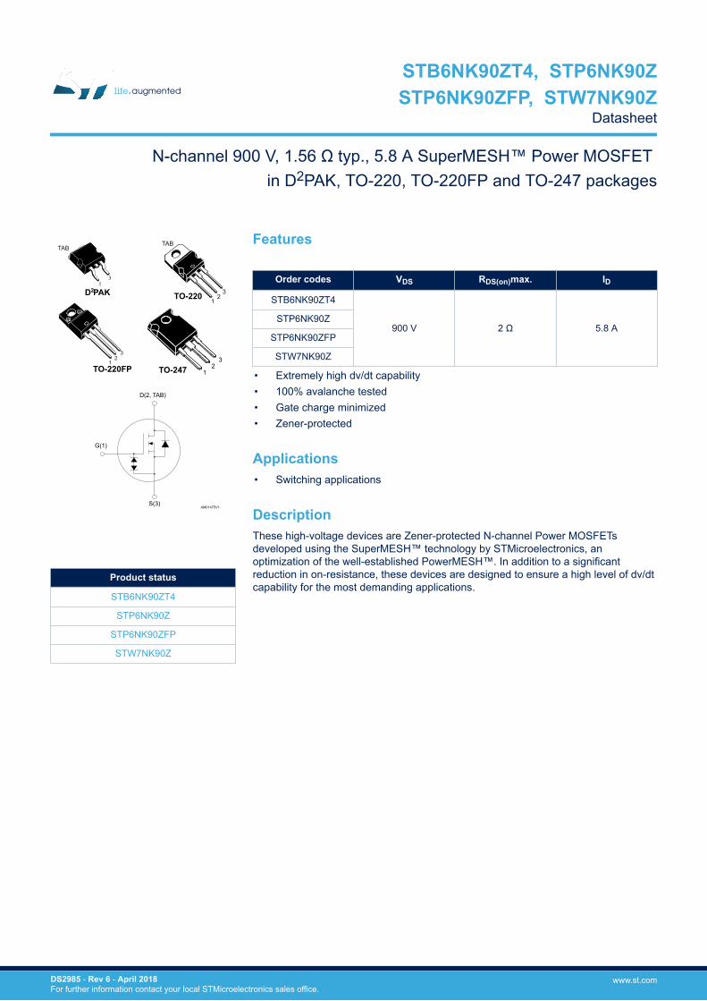
1 2 3 TO-247 1 2 3 TAB TO-220 1 3 TAB D PAK 2 1 2 3 TO-220FP D(2, TAB) G(1) S(3) AM01475V1 Features Order codes V DS R DS(on) max. I D STB6NK90ZT4 900 V 2 Ω 5.8 A STP6NK90Z STP6NK90ZFP STW7NK90Z • Extremely high dv/dt capability • 100% avalanche tested • Gate charge minimized • Zener-protected Applications • Switching applications Description These high-voltage devices are Zener-protected N-channel Power MOSFETs developed using the SuperMESH™ technology by STMicroelectronics, an optimization of the well-established PowerMESH™. In addition to a significant reduction in on-resistance, these devices are designed to ensure a high level of dv/dt capability for the most demanding applications. Product status STB6NK90ZT4 STP6NK90Z STP6NK90ZFP STW7NK90Z N-channel 900 V, 1.56 Ω typ., 5.8 A SuperMESH™ Power MOSFET in D 2 PAK, TO-220, TO-220FP and TO-247 packages STB6NK90ZT4, STP6NK90Z STP6NK90ZFP, STW7NK90Z Datasheet DS2985 - Rev 6 - April 2018 For further information contact your local STMicroelectronics sales office. www.st.com
Transcript of N-channel 900 V, 1.56 typ., 5.8 A SuperMESH Power … · 1 Electrical ratings Table 1. Absolute...
12
3
TO-247
12
3
TAB
TO-2201
3
TAB
D PAK2
12
3
TO-220FP
D(2, TAB)
G(1)
S(3)AM01475V1
Features
Order codes VDS RDS(on)max. ID
STB6NK90ZT4
900 V 2 Ω 5.8 ASTP6NK90Z
STP6NK90ZFP
STW7NK90Z
• Extremely high dv/dt capability• 100% avalanche tested• Gate charge minimized• Zener-protected
Applications• Switching applications
DescriptionThese high-voltage devices are Zener-protected N-channel Power MOSFETsdeveloped using the SuperMESH™ technology by STMicroelectronics, anoptimization of the well-established PowerMESH™. In addition to a significantreduction in on-resistance, these devices are designed to ensure a high level of dv/dtcapability for the most demanding applications.
Product status
STB6NK90ZT4
STP6NK90Z
STP6NK90ZFP
STW7NK90Z
N-channel 900 V, 1.56 Ω typ., 5.8 A SuperMESH™ Power MOSFET in D2PAK, TO-220, TO-220FP and TO-247 packages
STB6NK90ZT4, STP6NK90Z STP6NK90ZFP, STW7NK90Z
Datasheet
DS2985 - Rev 6 - April 2018For further information contact your local STMicroelectronics sales office.
www.st.com
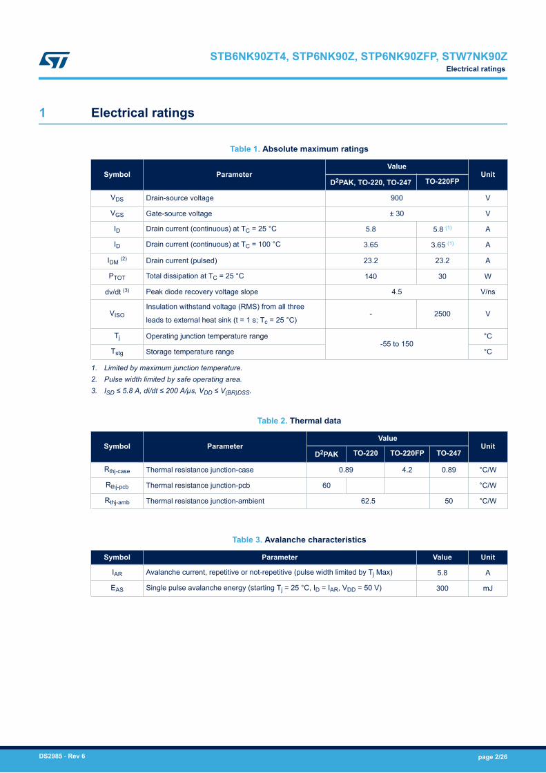
1 Electrical ratings
Table 1. Absolute maximum ratings
Symbol ParameterValue
UnitD2PAK, TO-220, TO-247 TO-220FP
VDS Drain-source voltage 900 V
VGS Gate-source voltage ± 30 V
ID Drain current (continuous) at TC = 25 °C 5.8 5.8 (1) A
ID Drain current (continuous) at TC = 100 °C 3.65 3.65 (1) A
IDM (2) Drain current (pulsed) 23.2 23.2 A
PTOT Total dissipation at TC = 25 °C 140 30 W
dv/dt (3) Peak diode recovery voltage slope 4.5 V/ns
VISOInsulation withstand voltage (RMS) from all three
leads to external heat sink (t = 1 s; Tc = 25 °C)- 2500 V
Tj Operating junction temperature range-55 to 150
°C
Tstg Storage temperature range °C
1. Limited by maximum junction temperature.2. Pulse width limited by safe operating area.3. ISD ≤ 5.8 A, di/dt ≤ 200 A/µs, VDD ≤ V(BR)DSS.
Table 2. Thermal data
Symbol ParameterValue
UnitD2PAK TO-220 TO-220FP TO-247
Rthj-case Thermal resistance junction-case 0.89 4.2 0.89 °C/W
Rthj-pcb Thermal resistance junction-pcb 60 °C/W
Rthj-amb Thermal resistance junction-ambient 62.5 50 °C/W
Table 3. Avalanche characteristics
Symbol Parameter Value Unit
IAR Avalanche current, repetitive or not-repetitive (pulse width limited by Tj Max) 5.8 A
EAS Single pulse avalanche energy (starting Tj = 25 °C, ID = IAR, VDD = 50 V) 300 mJ
STB6NK90ZT4, STP6NK90Z, STP6NK90ZFP, STW7NK90ZElectrical ratings
DS2985 - Rev 6 page 2/26

2 Electrical characteristics
(TCASE = 25 °C unless otherwise specified)
Table 4. On/off states
Symbol Parameter Test conditions Min. Typ. Max. Unit
V(BR)DSSDrain-source
ID = 1 mA, VGS = 0 V 900 VBreakdown voltage
IDSSZero gate voltage draincurrent
VGS = 0 V, VDS = 900 V 1 µA
VGS = 0 V, VDS = 900 V, TC = 125 °C (1) 50 µA
IGSSGate body leakagecurrent VDS = 0 V, VGS = ±20 V ±10 µA
VGS(th) Gate threshold voltage VDS = VGS, ID = 100 µA 3 3.75 4.5 V
RDS(on)Static drain-source onresistance VGS = 10 V, ID = 2.9 A 1.56 2 Ω
1. Defined by design, not subject to production test.
Table 5. Dynamic
Symbol Parameter Test conditions Min. Typ. Max. Unit
Ciss Input capacitance
VDS = 25 V, f = 1 MHz, VGS = 0 V
1350
pFCoss Output capacitance 130
CrssReverse transfercapacitance 26
Coss eq. (1) Equivalent outputcapacitance VGS = 0 V, VDS = 0 V to 720 V 70 pF
td(on) Turn-on delay timeVDD = 450 V, ID = 3 A, RG = 4.7 Ω,VGS = 10 V (see Figure 17. Test circuit forresistive load switching times and Figure22. Switching time waveform)
17
nstr Rise time 20
tr(off) Turn-off delay time 45
tr Fall time 20
Qg Total gate chargeVDD = 720 V, ID = 5.8 A, VGS = 0 to 10 V(see Figure 18. Test circuit for gate chargebehavior)
46.5 60.5
nCQgs Gate-source charge 8.5
Qgd Gate-drain charge 25
tr(Voff) Off-voltage rise time VDD = 720 V, ID = 5.8 A, RG = 4.7 Ω,VGS = 10 V (see Figure 19. Test circuit forinductive load switching and diode recoverytimes)
11
nstr Fall time 12
tc Cross-over time 20
1. Coss eq. is defined as a constant equivalent capacitance giving the same charging time as Coss when VDS increases from 0to 80% VDSS.
STB6NK90ZT4, STP6NK90Z, STP6NK90ZFP, STW7NK90ZElectrical characteristics
DS2985 - Rev 6 page 3/26
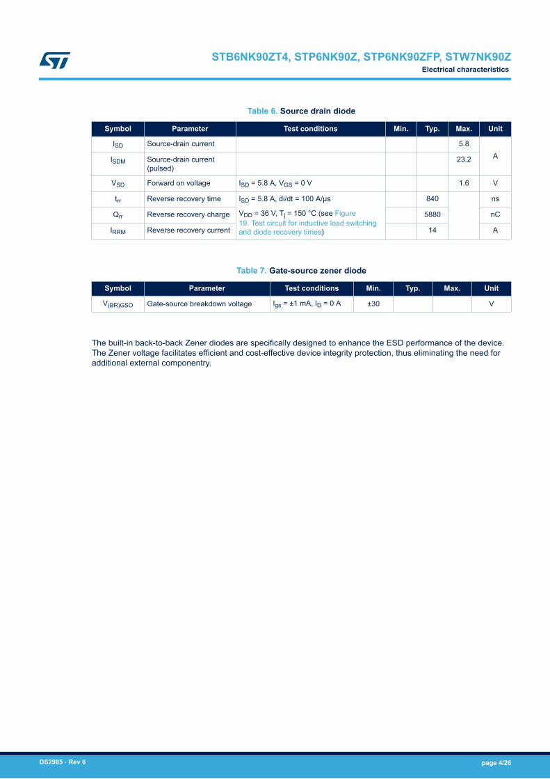
Table 6. Source drain diode
Symbol Parameter Test conditions Min. Typ. Max. Unit
ISD Source-drain current 5.8AISDM Source-drain current
(pulsed)23.2
VSD Forward on voltage ISD = 5.8 A, VGS = 0 V 1.6 V
trr Reverse recovery time ISD = 5.8 A, di/dt = 100 A/µs
VDD = 36 V, Tj = 150 °C (see Figure19. Test circuit for inductive load switchingand diode recovery times)
840 ns
Qrr Reverse recovery charge 5880 nC
IRRM Reverse recovery current 14 A
Table 7. Gate-source zener diode
Symbol Parameter Test conditions Min. Typ. Max. Unit
V(BR)GSO Gate-source breakdown voltage Igs = ±1 mA, ID = 0 A ±30 V
The built-in back-to-back Zener diodes are specifically designed to enhance the ESD performance of the device.The Zener voltage facilitates efficient and cost-effective device integrity protection, thus eliminating the need foradditional external componentry.
STB6NK90ZT4, STP6NK90Z, STP6NK90ZFP, STW7NK90ZElectrical characteristics
DS2985 - Rev 6 page 4/26

2.1 Electrical characteristics curves
Figure 1. Safe operating area for TO-220/D2PAK
GADG260320180900MT
Figure 2. Thermal impedance for TO-220/D2PAK
GADG260320180901MT
Figure 3. Safe operating area for TO-220FP
GADG260320180902MT
Figure 4. Thermal impedance for TO-220FP
GADG260320180903MT
Figure 5. Safe operating area for TO-247
GADG260320180904MT
Figure 6. Thermal impedance for TO-247
GADG260320180905MT
STB6NK90ZT4, STP6NK90Z, STP6NK90ZFP, STW7NK90ZElectrical characteristics curves
DS2985 - Rev 6 page 5/26

Figure 7. Output characterisics
GADG260320180906MT
Figure 8. Transfer characteristics
GADG260320180907MT
Figure 9. Static drain-source on resistance
GADG260320180909MT
Figure 10. Gate charge vs gate-source voltage
GADG260320180910MT
Figure 11. Capacitance variations
GADG260320180911MT
Figure 12. Normalized gate threshold voltage vstemperature
GADG260320180912MT
STB6NK90ZT4, STP6NK90Z, STP6NK90ZFP, STW7NK90ZElectrical characteristics curves
DS2985 - Rev 6 page 6/26

Figure 13. Normalized on resistance vs temperature
GADG260320180913MT
Figure 14. Source-drain diode forward characteristic
GADG260320180914MT
Figure 15. Normalized V(BR)DSS vs temperature
GADG260320180915MT
Figure 16. Maximum avalanche energy vs temperature
GADG260320180916MT
STB6NK90ZT4, STP6NK90Z, STP6NK90ZFP, STW7NK90ZElectrical characteristics curves
DS2985 - Rev 6 page 7/26
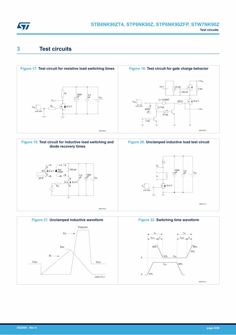
3 Test circuits
Figure 17. Test circuit for resistive load switching times
AM01468v1
VD
RG
RL
D.U.T.
2200μF VDD
3.3μF+
pulse width
VGS
Figure 18. Test circuit for gate charge behavior
AM01469v1
47 kΩ1 kΩ
47 kΩ
2.7 kΩ
1 kΩ
12 V
IG= CONST100 Ω
100 nF
D.U.T.
+pulse width
VGS
2200μF
VG
VDD
Figure 19. Test circuit for inductive load switching anddiode recovery times
AM01470v1
AD
D.U.T.S
B
G
25 Ω
A A
B B
RG
GD
S
100 µH
µF3.3 1000
µF VDD
D.U.T.
+
_
+
fastdiode
Figure 20. Unclamped inductive load test circuit
AM01471v1
VD
ID
D.U.T.
L
VDD+
pulse width
Vi
3.3µF
2200µF
Figure 21. Unclamped inductive waveform
AM01472v1
V(BR)DSS
VDDVDD
VD
IDM
ID
Figure 22. Switching time waveform
AM01473v1
0
VGS 90%
VDS
90%
10%
90%
10%
10%
ton
td(on) tr
0
toff
td(off) tf
STB6NK90ZT4, STP6NK90Z, STP6NK90ZFP, STW7NK90ZTest circuits
DS2985 - Rev 6 page 8/26

4 Package information
In order to meet environmental requirements, ST offers these devices in different grades of ECOPACK®
packages, depending on their level of environmental compliance. ECOPACK® specifications, grade definitionsand product status are available at: www.st.com. ECOPACK® is an ST trademark.
STB6NK90ZT4, STP6NK90Z, STP6NK90ZFP, STW7NK90ZPackage information
DS2985 - Rev 6 page 9/26

4.1 D²PAK (TO-263) package information
Figure 23. D²PAK (TO-263) type A package outline
0079457_24
STB6NK90ZT4, STP6NK90Z, STP6NK90ZFP, STW7NK90ZD²PAK (TO-263) package information
DS2985 - Rev 6 page 10/26

Table 8. D²PAK (TO-263) type A package mechanical data
Dim.mm
Min. Typ. Max.
A 4.40 4.60
A1 0.03 0.23
b 0.70 0.93
b2 1.14 1.70
c 0.45 0.60
c2 1.23 1.36
D 8.95 9.35
D1 7.50 7.75 8.00
D2 1.10 1.30 1.50
E 10.00 10.40
E1 8.50 8.70 8.90
E2 6.85 7.05 7.25
e 2.54
e1 4.88 5.28
H 15.00 15.85
J1 2.49 2.69
L 2.29 2.79
L1 1.27 1.40
L2 1.30 1.75
R 0.40
V2 0° 8°
STB6NK90ZT4, STP6NK90Z, STP6NK90ZFP, STW7NK90ZD²PAK (TO-263) package information
DS2985 - Rev 6 page 11/26
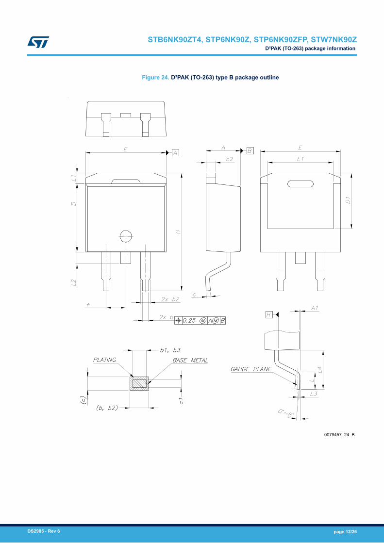
Figure 24. D²PAK (TO-263) type B package outline
0079457_24_B
STB6NK90ZT4, STP6NK90Z, STP6NK90ZFP, STW7NK90ZD²PAK (TO-263) package information
DS2985 - Rev 6 page 12/26

Table 9. D²PAK (TO-263) type B mechanical data
Dim.mm
Min. Typ. Max.
A 4.36 4.56
A1 0 0.25
b 0.70 0.90
b1 0.51 0.89
b2 1.17 1.37
b3 1.36 1.46
c 0.38 0.694
c1 0.38 0.534
c2 1.19 1.34
D 8.60 9.00
D1 6.90 7.50
E 10.15 10.55
E1 8.10 8.70
e 2.54 BSC
H 15.00 15.60
L 1.90 2.50
L1 1.65
L2 1.78
L3 0.25
L4 4.78 5.28
STB6NK90ZT4, STP6NK90Z, STP6NK90ZFP, STW7NK90ZD²PAK (TO-263) package information
DS2985 - Rev 6 page 13/26

Figure 25. D²PAK (TO-263) recommended footprint (dimensions are in mm)
Footprint
STB6NK90ZT4, STP6NK90Z, STP6NK90ZFP, STW7NK90ZD²PAK (TO-263) package information
DS2985 - Rev 6 page 14/26

4.2 TO-220 type A package information
Figure 26. TO-220 type A package outline
0015988_typeA_Rev_21
STB6NK90ZT4, STP6NK90Z, STP6NK90ZFP, STW7NK90ZTO-220 type A package information
DS2985 - Rev 6 page 15/26

Table 10. TO-220 type A package mechanical data
Dim.mm
Min. Typ. Max.
A 4.40 4.60
b 0.61 0.88
b1 1.14 1.55
c 0.48 0.70
D 15.25 15.75
D1 1.27
E 10.00 10.40
e 2.40 2.70
e1 4.95 5.15
F 1.23 1.32
H1 6.20 6.60
J1 2.40 2.72
L 13.00 14.00
L1 3.50 3.93
L20 16.40
L30 28.90
øP 3.75 3.85
Q 2.65 2.95
STB6NK90ZT4, STP6NK90Z, STP6NK90ZFP, STW7NK90ZTO-220 type A package information
DS2985 - Rev 6 page 16/26

4.3 TO-220 type H package information
Figure 27. TO-220 type H package outline
0015988_H_21
STB6NK90ZT4, STP6NK90Z, STP6NK90ZFP, STW7NK90ZTO-220 type H package information
DS2985 - Rev 6 page 17/26
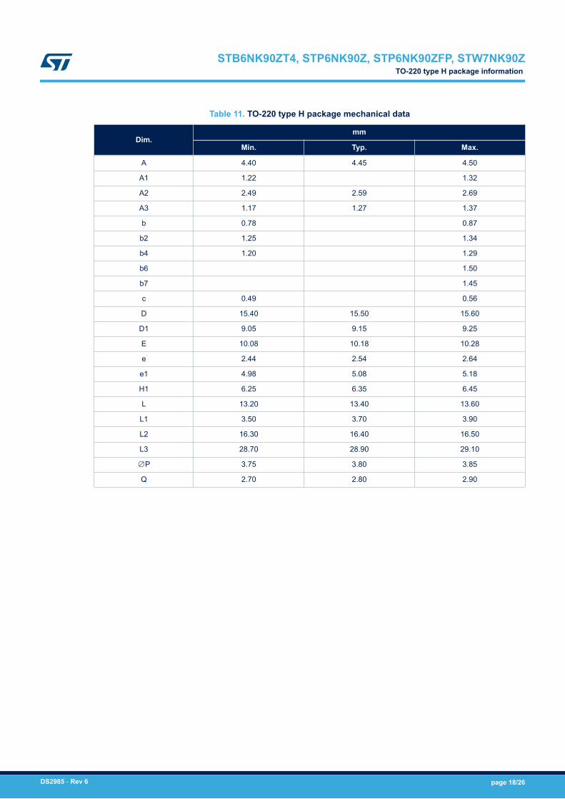
Table 11. TO-220 type H package mechanical data
Dim.mm
Min. Typ. Max.
A 4.40 4.45 4.50
A1 1.22 1.32
A2 2.49 2.59 2.69
A3 1.17 1.27 1.37
b 0.78 0.87
b2 1.25 1.34
b4 1.20 1.29
b6 1.50
b7 1.45
c 0.49 0.56
D 15.40 15.50 15.60
D1 9.05 9.15 9.25
E 10.08 10.18 10.28
e 2.44 2.54 2.64
e1 4.98 5.08 5.18
H1 6.25 6.35 6.45
L 13.20 13.40 13.60
L1 3.50 3.70 3.90
L2 16.30 16.40 16.50
L3 28.70 28.90 29.10
∅P 3.75 3.80 3.85
Q 2.70 2.80 2.90
STB6NK90ZT4, STP6NK90Z, STP6NK90ZFP, STW7NK90ZTO-220 type H package information
DS2985 - Rev 6 page 18/26

4.4 TO-220FP package information
Figure 28. TO-220FP package outline
7012510_Rev_12_B
STB6NK90ZT4, STP6NK90Z, STP6NK90ZFP, STW7NK90ZTO-220FP package information
DS2985 - Rev 6 page 19/26

Table 12. TO-220FP package mechanical data
Dim.mm
Min. Typ. Max.
A 4.4 4.6
B 2.5 2.7
D 2.5 2.75
E 0.45 0.7
F 0.75 1
F1 1.15 1.70
F2 1.15 1.70
G 4.95 5.2
G1 2.4 2.7
H 10 10.4
L2 16
L3 28.6 30.6
L4 9.8 10.6
L5 2.9 3.6
L6 15.9 16.4
L7 9 9.3
Dia 3 3.2
STB6NK90ZT4, STP6NK90Z, STP6NK90ZFP, STW7NK90ZTO-220FP package information
DS2985 - Rev 6 page 20/26

4.5 TO-247 package information
Figure 29. TO-247 package outline
0075325_9
STB6NK90ZT4, STP6NK90Z, STP6NK90ZFP, STW7NK90ZTO-247 package information
DS2985 - Rev 6 page 21/26
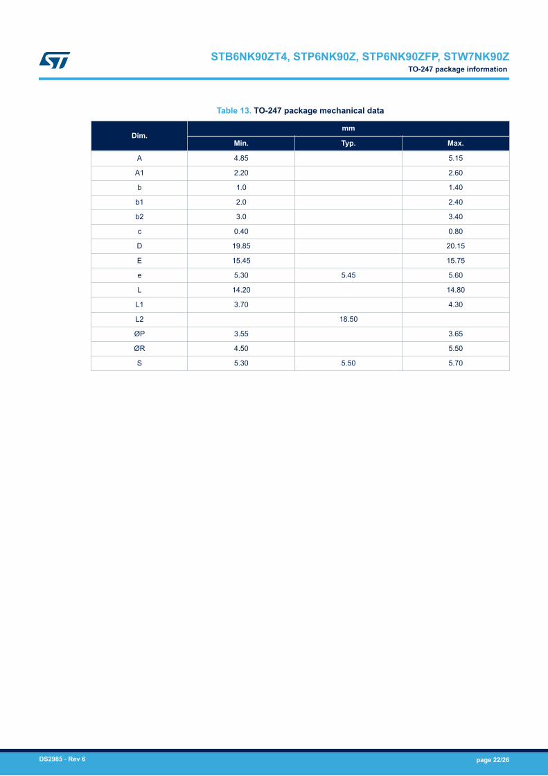
Table 13. TO-247 package mechanical data
Dim.mm
Min. Typ. Max.
A 4.85 5.15
A1 2.20 2.60
b 1.0 1.40
b1 2.0 2.40
b2 3.0 3.40
c 0.40 0.80
D 19.85 20.15
E 15.45 15.75
e 5.30 5.45 5.60
L 14.20 14.80
L1 3.70 4.30
L2 18.50
ØP 3.55 3.65
ØR 4.50 5.50
S 5.30 5.50 5.70
STB6NK90ZT4, STP6NK90Z, STP6NK90ZFP, STW7NK90ZTO-247 package information
DS2985 - Rev 6 page 22/26
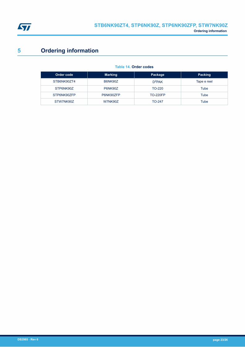
5 Ordering information
Table 14. Order codes
Order code Marking Package Packing
STB6NK90ZT4 B6NK90Z D2PAK Tape e reel
STP6NK90Z P6NK90Z TO-220 Tube
STP6NK90ZFP P6NK90ZFP TO-220FP Tube
STW7NK90Z W7NK90Z TO-247 Tube
STB6NK90ZT4, STP6NK90Z, STP6NK90ZFP, STW7NK90ZOrdering information
DS2985 - Rev 6 page 23/26

Revision history
Table 15. Document revision history
Date Version Changes
29-Nov-2005 3 Complete version
16-Aug-2006 4 New template, no content change
10-Apr-2007 5 Typo mistake on Table 2
04-Apr-2018 6
Removed maturity status indication from cover page. The document status isproduction data.
Updated Table 5. Dynamic and Table 6. Source drain diode.
Minor text changes.
STB6NK90ZT4, STP6NK90Z, STP6NK90ZFP, STW7NK90Z
DS2985 - Rev 6 page 24/26

Contents
1 Electrical ratings . . . . . . . . . . . . . . . . . . . . . . . . . . . . . . . . . . . . . . . . . . . . . . . . . . . . . . . . . . . . . . . . . .2
2 Electrical characteristics. . . . . . . . . . . . . . . . . . . . . . . . . . . . . . . . . . . . . . . . . . . . . . . . . . . . . . . . . . .3
2.1 Electrical characteristics curves . . . . . . . . . . . . . . . . . . . . . . . . . . . . . . . . . . . . . . . . . . . . . . . . . . 5
3 Test circuits . . . . . . . . . . . . . . . . . . . . . . . . . . . . . . . . . . . . . . . . . . . . . . . . . . . . . . . . . . . . . . . . . . . . . . .8
4 Package information. . . . . . . . . . . . . . . . . . . . . . . . . . . . . . . . . . . . . . . . . . . . . . . . . . . . . . . . . . . . . . .9
4.1 D²PAK (TO-263) package information . . . . . . . . . . . . . . . . . . . . . . . . . . . . . . . . . . . . . . . . . . . . . 9
4.2 TO-220 type A package information. . . . . . . . . . . . . . . . . . . . . . . . . . . . . . . . . . . . . . . . . . . . . . 14
4.3 TO-220 type H package information. . . . . . . . . . . . . . . . . . . . . . . . . . . . . . . . . . . . . . . . . . . . . . 16
4.4 TO-220FP package information . . . . . . . . . . . . . . . . . . . . . . . . . . . . . . . . . . . . . . . . . . . . . . . . . 18
4.5 TO-247 package information. . . . . . . . . . . . . . . . . . . . . . . . . . . . . . . . . . . . . . . . . . . . . . . . . . . . 20
5 Ordering information . . . . . . . . . . . . . . . . . . . . . . . . . . . . . . . . . . . . . . . . . . . . . . . . . . . . . . . . . . . . .23
Revision history . . . . . . . . . . . . . . . . . . . . . . . . . . . . . . . . . . . . . . . . . . . . . . . . . . . . . . . . . . . . . . . . . . . . . . .24
STB6NK90ZT4, STP6NK90Z, STP6NK90ZFP, STW7NK90ZContents
DS2985 - Rev 6 page 25/26
IMPORTANT NOTICE – PLEASE READ CAREFULLY
STMicroelectronics NV and its subsidiaries (“ST”) reserve the right to make changes, corrections, enhancements, modifications, and improvements to STproducts and/or to this document at any time without notice. Purchasers should obtain the latest relevant information on ST products before placing orders. STproducts are sold pursuant to ST’s terms and conditions of sale in place at the time of order acknowledgement.
Purchasers are solely responsible for the choice, selection, and use of ST products and ST assumes no liability for application assistance or the design ofPurchasers’ products.
No license, express or implied, to any intellectual property right is granted by ST herein.
Resale of ST products with provisions different from the information set forth herein shall void any warranty granted by ST for such product.
ST and the ST logo are trademarks of ST. All other product or service names are the property of their respective owners.
Information in this document supersedes and replaces information previously supplied in any prior versions of this document.
© 2018 STMicroelectronics – All rights reserved
STB6NK90ZT4, STP6NK90Z, STP6NK90ZFP, STW7NK90Z
DS2985 - Rev 6 page 26/26