![Ç o v^ ] } v · î ô &ODVV](https://static.fdocument.org/doc/165x107/621c22aaeca1c872404f6486/-o-v-v-ampodvv.jpg)
N-channel 800 V, 0.3 typ., 14 A MDmesh K5 Power ...ISD ≤ 14 A, di/dt ≤ 100 A/µs, VPeak ≤...
23
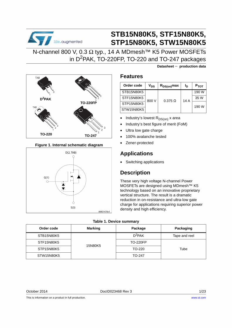
This is information on a product in full production. October 2014 DocID023468 Rev 3 1/23 23 STB15N80K5, STF15N80K5, STP15N80K5, STW15N80K5 N-channel 800 V, 0.3 Ω typ., 14 A MDmesh™ K5 Power MOSFETs in D 2 PAK, TO-220FP, TO-220 and TO-247 packages Datasheet − production data Figure 1. Internal schematic diagram Features • Industry’s lowest R DS(on) x area • Industry’s best figure of merit (FoM) • Ultra low gate charge • 100% avalanche tested • Zener-protected Applications • Switching applications Description These very high voltage N-channel Power MOSFETs are designed using MDmesh™ K5 technology based on an innovative proprietary vertical structure. The result is a dramatic reduction in on-resistance and ultra-low gate charge for applications requiring superior power density and high efficiency. D(2, TAB) G(1) S(3) AM01476v1 TO-220 1 2 3 TAB 1 2 3 TO-220FP TO-247 1 3 TAB D 2 PAK 1 2 3 Order code V DS R DS(on) max I D P TOT STB15N80K5 800 V 0.375 Ω 14 A 190 W STF15N80K5 35 W STP15N80K5 190 W STW15N80K5 Table 1. Device summary Order code Marking Package Packaging STB15N80K5 15N80K5 D 2 PAK Tape and reel STF15N80K5 TO-220FP Tube STP15N80K5 TO-220 STW15N80K5 TO-247 www.st.com
Transcript of N-channel 800 V, 0.3 typ., 14 A MDmesh K5 Power ...ISD ≤ 14 A, di/dt ≤ 100 A/µs, VPeak ≤...
This is information on a product in full production.
October 2014 DocID023468 Rev 3 1/23
23
STB15N80K5, STF15N80K5, STP15N80K5, STW15N80K5
N-channel 800 V, 0.3 Ω typ., 14 A MDmesh™ K5 Power MOSFETs in D2PAK, TO-220FP, TO-220 and TO-247 packages
Datasheet − production data
Figure 1. Internal schematic diagram
Features
• Industry’s lowest RDS(on) x area
• Industry’s best figure of merit (FoM)
• Ultra low gate charge
• 100% avalanche tested
• Zener-protected
Applications• Switching applications
DescriptionThese very high voltage N-channel Power MOSFETs are designed using MDmesh™ K5 technology based on an innovative proprietary vertical structure. The result is a dramatic reduction in on-resistance and ultra-low gate charge for applications requiring superior power density and high efficiency.
D(2, TAB)
G(1)
S(3)AM01476v1
TO-2201
23
TAB
12
3
TO-220FP
TO-247
13
TAB
D2PAK 12
3
Order code VDS RDS(on)max ID PTOT
STB15N80K5
800 V 0.375 Ω 14 A
190 W
STF15N80K5 35 W
STP15N80K5190 W
STW15N80K5
Table 1. Device summary
Order code Marking Package Packaging
STB15N80K5
15N80K5
D2PAK Tape and reel
STF15N80K5 TO-220FP
TubeSTP15N80K5 TO-220
STW15N80K5 TO-247
www.st.com
Contents STB15N80K5, STF15N80K5, STP15N80K5, STW15N80K5
2/23 DocID023468 Rev 3
Contents
1 Electrical ratings . . . . . . . . . . . . . . . . . . . . . . . . . . . . . . . . . . . . . . . . . . . . 3
2 Electrical characteristics . . . . . . . . . . . . . . . . . . . . . . . . . . . . . . . . . . . . . 4
2.1 Electrical characteristics (curves) . . . . . . . . . . . . . . . . . . . . . . . . . . . . . . . . 6
3 Test circuits . . . . . . . . . . . . . . . . . . . . . . . . . . . . . . . . . . . . . . . . . . . . . . 9
4 Package mechanical data . . . . . . . . . . . . . . . . . . . . . . . . . . . . . . . . . . . . 10
4.1 STB15N80K5, D²PAK (TO-263) . . . . . . . . . . . . . . . . . . . . . . . . . . . . . . . . .11
4.2 STP15N80K5, TO-220 . . . . . . . . . . . . . . . . . . . . . . . . . . . . . . . . . . . . . . . 14
4.3 STF15N80K5, TO-220FP . . . . . . . . . . . . . . . . . . . . . . . . . . . . . . . . . . . . . 16
4.4 STW15N80K5, TO-247 . . . . . . . . . . . . . . . . . . . . . . . . . . . . . . . . . . . . . . 18
5 Packaging information . . . . . . . . . . . . . . . . . . . . . . . . . . . . . . . . . . . . . . 20
6 Revision history . . . . . . . . . . . . . . . . . . . . . . . . . . . . . . . . . . . . . . . . . . . 22
DocID023468 Rev 3 3/23
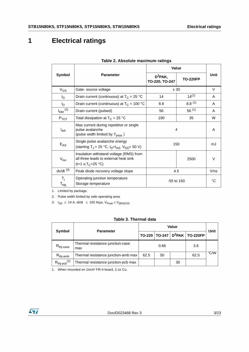
STB15N80K5, STF15N80K5, STP15N80K5, STW15N80K5 Electrical ratings
1 Electrical ratings
Table 2. Absolute maximum ratings
Symbol Parameter
Value
UnitD2PAK, TO-220, TO-247
TO-220FP
VGS Gate- source voltage ± 30 V
ID Drain current (continuous) at TC = 25 °C 14 14(1)
1. Limited by package.
A
ID Drain current (continuous) at TC = 100 °C 8.8 8.8 (1) A
IDM (2)
2. Pulse width limited by safe operating area.
Drain current (pulsed) 56 56 (1) A
PTOT Total dissipation at TC = 25 °C 190 35 W
IAR
Max current during repetitive or single pulse avalanche (pulse width limited by Tjmax )
4 A
EASSingle pulse avalanche energy (starting TJ = 25 °C, ID=IAS, VDD= 50 V)
150 mJ
Viso
Insulation withstand voltage (RMS) from all three leads to external heat sink
(t=1 s;TC=25 °C)2500 V
dv/dt (3)
3. ISD ≤ 14 A, di/dt ≤ 100 A/µs, VPeak ≤ V(BR)DSS
Peak diode recovery voltage slope 4.5 V/ns
Tj
Tstg
Operating junction temperatureStorage temperature
-55 to 150 °C
Table 3. Thermal data
Symbol ParameterValue
UnitTO-220 TO-247 D2PAK TO-220FP
Rthj-caseThermal resistance junction-case max
0.66 3.6
°C/WRthj-amb Thermal resistance junction-amb max 62.5 50 62.5
Rthj-pcb(1)
1. When mounted on 1inch² FR-4 board, 2 oz Cu.
Thermal resistance junction-pcb max 30
Electrical characteristics STB15N80K5, STF15N80K5, STP15N80K5, STW15N80K5
4/23 DocID023468 Rev 3
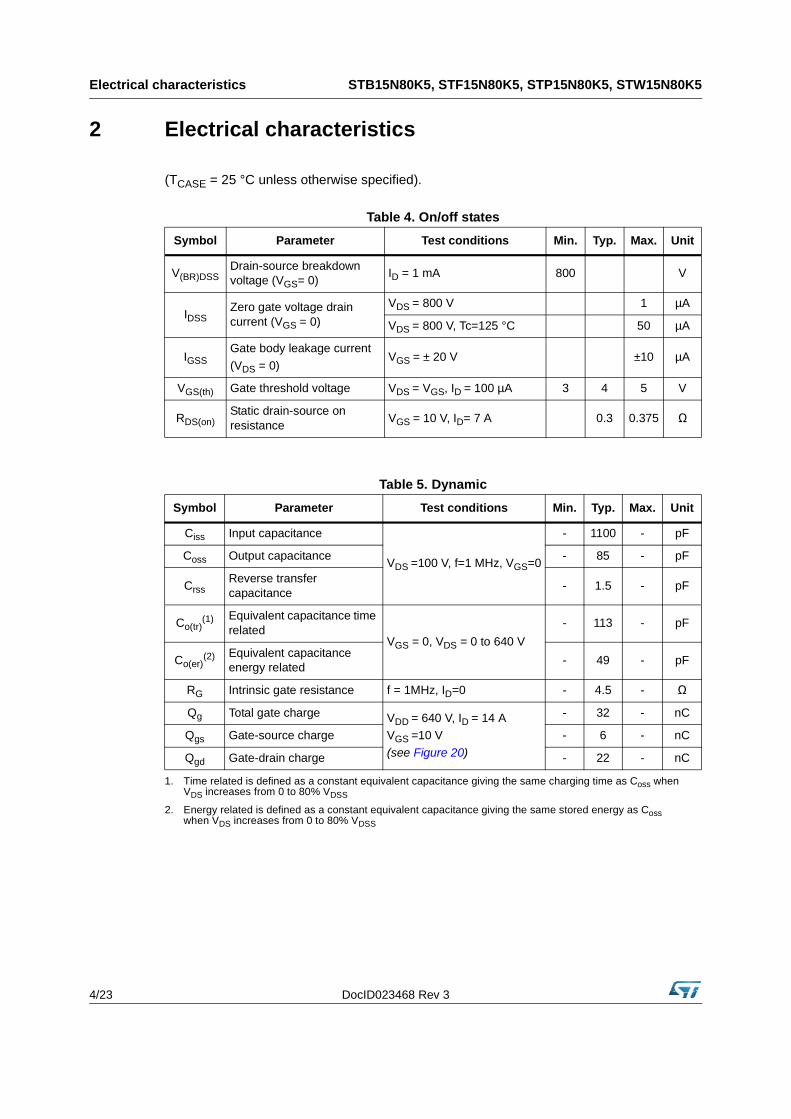
2 Electrical characteristics
(TCASE = 25 °C unless otherwise specified).
Table 4. On/off states
Symbol Parameter Test conditions Min. Typ. Max. Unit
V(BR)DSSDrain-source breakdown voltage (VGS= 0)
ID = 1 mA 800 V
IDSSZero gate voltage drain current (VGS = 0)
VDS = 800 V 1 µA
VDS = 800 V, Tc=125 °C 50 µA
IGSSGate body leakage current
(VDS = 0)VGS = ± 20 V ±10 µA
VGS(th) Gate threshold voltage VDS = VGS, ID = 100 µA 3 4 5 V
RDS(on)Static drain-source on resistance
VGS = 10 V, ID= 7 A 0.3 0.375 Ω
Table 5. Dynamic
Symbol Parameter Test conditions Min. Typ. Max. Unit
Ciss Input capacitance
VDS =100 V, f=1 MHz, VGS=0
- 1100 - pF
Coss Output capacitance - 85 - pF
CrssReverse transfer capacitance
- 1.5 - pF
Co(tr)(1)
1. Time related is defined as a constant equivalent capacitance giving the same charging time as Coss when VDS increases from 0 to 80% VDSS
Equivalent capacitance time related
VGS = 0, VDS = 0 to 640 V
- 113 - pF
Co(er)(2)
2. Energy related is defined as a constant equivalent capacitance giving the same stored energy as Coss when VDS increases from 0 to 80% VDSS
Equivalent capacitance energy related
- 49 - pF
RG Intrinsic gate resistance f = 1MHz, ID=0 - 4.5 - Ω
Qg Total gate charge VDD = 640 V, ID = 14 A VGS =10 V
(see Figure 20)
- 32 - nC
Qgs Gate-source charge - 6 - nC
Qgd Gate-drain charge - 22 - nC
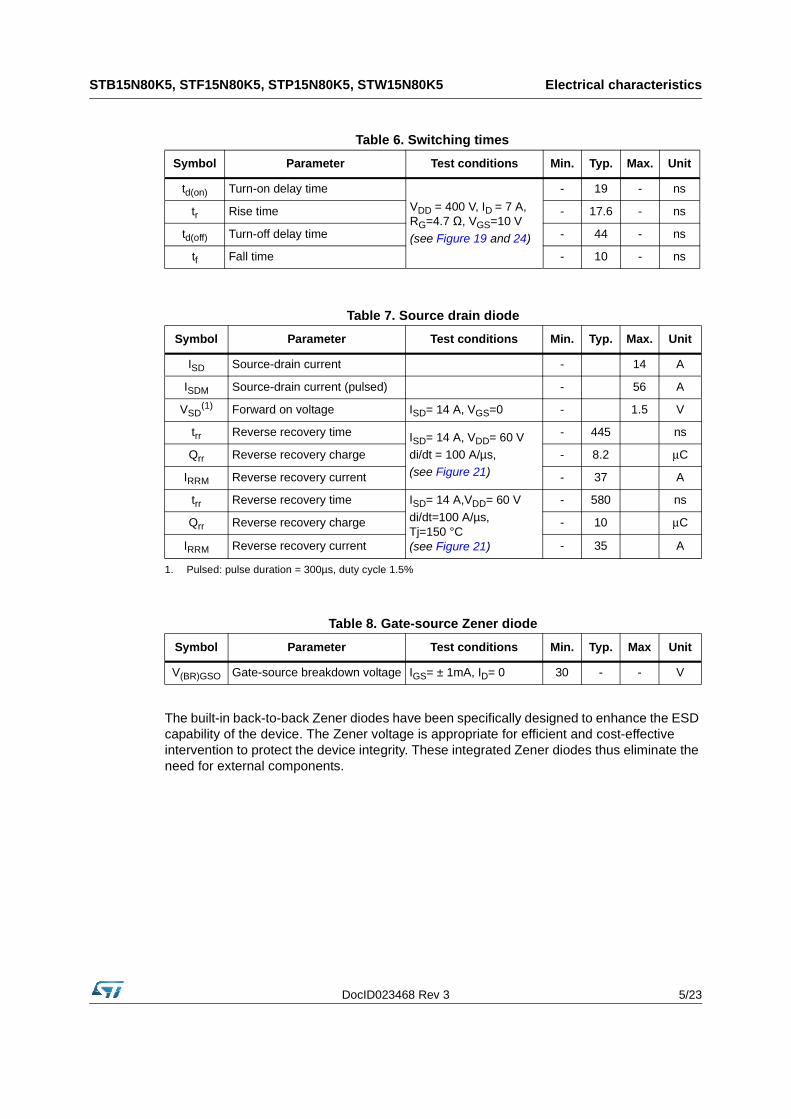
DocID023468 Rev 3 5/23
STB15N80K5, STF15N80K5, STP15N80K5, STW15N80K5 Electrical characteristics
The built-in back-to-back Zener diodes have been specifically designed to enhance the ESD capability of the device. The Zener voltage is appropriate for efficient and cost-effective intervention to protect the device integrity. These integrated Zener diodes thus eliminate the need for external components.
Table 6. Switching times
Symbol Parameter Test conditions Min. Typ. Max. Unit
td(on) Turn-on delay time
VDD = 400 V, ID = 7 A, RG=4.7 Ω, VGS=10 V
(see Figure 19 and 24)
- 19 - ns
tr Rise time - 17.6 - ns
td(off) Turn-off delay time - 44 - ns
tf Fall time - 10 - ns
Table 7. Source drain diode
Symbol Parameter Test conditions Min. Typ. Max. Unit
ISD Source-drain current - 14 A
ISDM Source-drain current (pulsed) - 56 A
VSD(1)
1. Pulsed: pulse duration = 300µs, duty cycle 1.5%
Forward on voltage ISD= 14 A, VGS=0 - 1.5 V
trr Reverse recovery time ISD= 14 A, VDD= 60 Vdi/dt = 100 A/µs,(see Figure 21)
- 445 ns
Qrr Reverse recovery charge - 8.2 μC
IRRM Reverse recovery current - 37 A
trr Reverse recovery time ISD= 14 A,VDD= 60 V
di/dt=100 A/µs, Tj=150 °C(see Figure 21)
- 580 ns
Qrr Reverse recovery charge - 10 μC
IRRM Reverse recovery current - 35 A
Table 8. Gate-source Zener diode
Symbol Parameter Test conditions Min. Typ. Max Unit
V(BR)GSO Gate-source breakdown voltage IGS= ± 1mA, ID= 0 30 - - V
Electrical characteristics STB15N80K5, STF15N80K5, STP15N80K5, STW15N80K5
6/23 DocID023468 Rev 3
2.1 Electrical characteristics (curves)
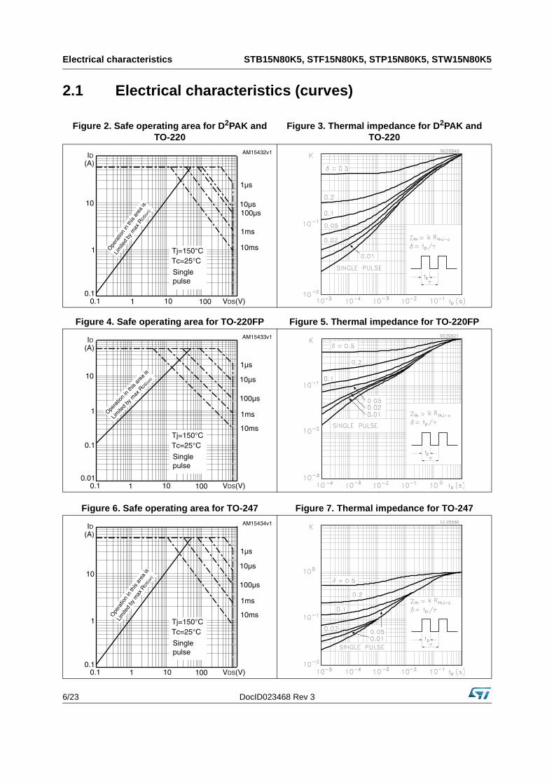
Figure 2. Safe operating area for D2PAK and TO-220
Figure 3. Thermal impedance for D2PAK and TO-220
Figure 4. Safe operating area for TO-220FP Figure 5. Thermal impedance for TO-220FP
ID
10
1
1 100 VDS(V)10
(A)
Ope
ratio
n in
this
area
is
Lim
ited
by m
ax R
DS(on
)
1µs
10µs100µs
10msTj=150°CTc=25°C
Singlepulse
1ms
0.10.1
AM15432v1
ID
10
1
0.1
1 100 VDS(V)10
(A)
Opera
tion
in th
is ar
ea is
Limite
d by
max
RDS(o
n)
1µs
10µs
100µs
10msTj=150°CTc=25°C
Singlepulse
1ms
0.10.01
AM15433v1
Figure 6. Safe operating area for TO-247 Figure 7. Thermal impedance for TO-247
ID
10
1
1 100 VDS(V)10
(A)
Ope
ratio
n in
this
area
is
Lim
ited
by m
ax R
DS(on
)
1µs
10µs
100µs
10msTj=150°CTc=25°C
Singlepulse
1ms
0.10.1
AM15434v1
DocID023468 Rev 3 7/23
STB15N80K5, STF15N80K5, STP15N80K5, STW15N80K5 Electrical characteristics
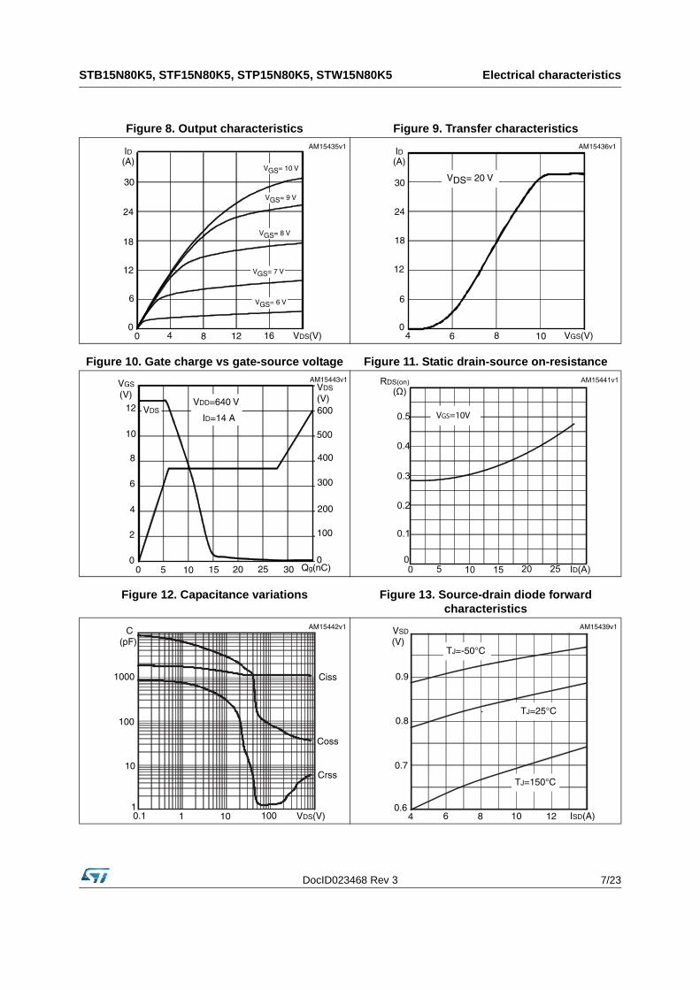
Figure 8. Output characteristics Figure 9. Transfer characteristics
Figure 10. Gate charge vs gate-source voltage Figure 11. Static drain-source on-resistance
Figure 12. Capacitance variations Figure 13. Source-drain diode forward characteristics
ID
24
12
00 8 VDS(V)16
(A)
4 12
VGS= 6 V
VGS= 7 V
VGS= 8 V
VGS= 9 V
6
18
30
VGS= 10 V
AM15435v1ID
18
12
6
0VGS(V)
(A)
4 6 8
24
10
VDS= 20 V30
AM15436v1
VGS
6
4
2
00 5 Qg(nC)
(V)
20
8
10 15
10
VDD=640 V
ID=14 A
25
300
200
100
0
400
500
VDS
(V)VDS12
30
600
AM15443v1 RDS(on)
0.3
0.2
0.1
00 10 ID(A)
(Ω)
5 15
VGS=10V0.5
0.4
20 25
AM15441v1
C
1000
100
10
10.1 10 VDS(V)
(pF)
1 100
Ciss
Coss
Crss
AM15442v1
VSD
4 ISD(A)
(V)
106 80.6
0.7
0.8
0.9
TJ=-50°C
TJ=150°C
TJ=25°C
12
AM15439v1
Electrical characteristics STB15N80K5, STF15N80K5, STP15N80K5, STW15N80K5
8/23 DocID023468 Rev 3
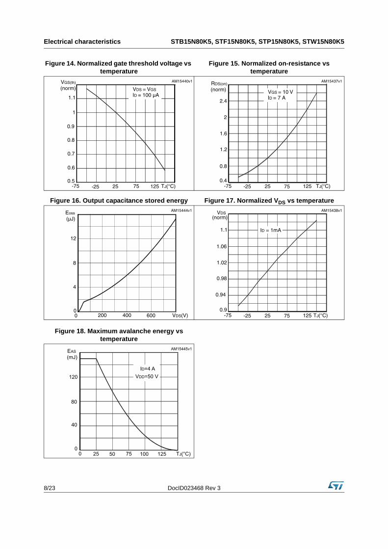
Figure 14. Normalized gate threshold voltage vs temperature
Figure 15. Normalized on-resistance vs temperature
Figure 16. Output capacitance stored energy Figure 17. Normalized VDS vs temperature
VGS(th)
0.8
0.7
0.6
0.5-75 TJ(°C)
(norm)
-25
0.9
7525 125
ID = 100 µAVDS = VGS
1
1.1
AM15440v1 RDS(on)
2
1.2
0.4-75 TJ(°C)
(norm)
-25 7525 125
0.8
1.6
2.4ID = 7 AVGS = 10 V
AM15437v1
Eoss
4
00 VDS(V)
(µJ)
400200
8
600
12
AM15444v1 VDS
TJ(°C)
ID = 1mA
0.98
0.9-75 -25 7525 125
0.94
1.02
1.06
1.1
(norm)AM15438v1
Figure 18. Maximum avalanche energy vs temperature

DocID023468 Rev 3 9/23
STB15N80K5, STF15N80K5, STP15N80K5, STW15N80K5 Test circuits
3 Test circuits
Figure 19. Switching times test circuit for resistive load
Figure 20. Gate charge test circuit
Figure 21. Test circuit for inductive load switching and diode recovery times
Figure 22. Unclamped inductive load test circuit
Figure 23. Unclamped inductive waveform Figure 24. Switching time waveform
AM01468v1
VGS
PW
VD
RG
RL
D.U.T.
2200
μF3.3μF
VDD
AM01469v1
VDD
47kΩ 1kΩ
47kΩ
2.7kΩ
1kΩ
12V
Vi=20V=VGMAX
2200μF
PW
IG=CONST100Ω
100nF
D.U.T.
VG
AM01470v1
AD
D.U.T.
SB
G
25 Ω
A A
BB
RG
G
FASTDIODE
D
S
L=100μH
μF3.3 1000
μF VDD
AM01471v1
Vi
Pw
VD
ID
D.U.T.
L
2200μF
3.3μF VDD
AM01472v1
V(BR)DSS
VDDVDD
VD
IDM
ID
AM01473v1
VDS
ton
tdon tdoff
toff
tftr
90%
10%
10%
0
0
90%
90%
10%
VGS
Package mechanical data STB15N80K5, STF15N80K5, STP15N80K5, STW15N80K5
10/23 DocID023468 Rev 3
4 Package mechanical data
In order to meet environmental requirements, ST offers these devices in different grades of ECOPACK® packages, depending on their level of environmental compliance. ECOPACK® specifications, grade definitions and product status are available at: www.st.com. ECOPACK® is an ST trademark.
DocID023468 Rev 3 11/23
STB15N80K5, STF15N80K5, STP15N80K5, STW15N80K5 Package mechanical data
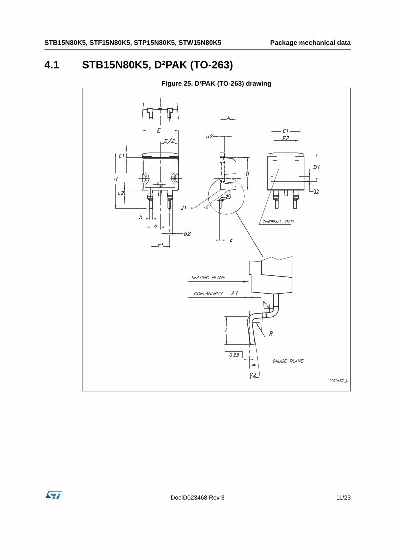
4.1 STB15N80K5, D²PAK (TO-263)
Figure 25. D²PAK (TO-263) drawing
0079457_U
Package mechanical data STB15N80K5, STF15N80K5, STP15N80K5, STW15N80K5
12/23 DocID023468 Rev 3
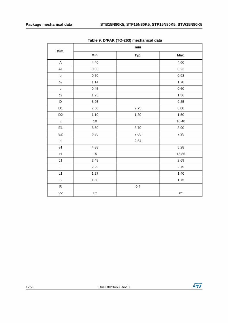
Table 9. D²PAK (TO-263) mechanical data
Dim.mm
Min. Typ. Max.
A 4.40 4.60
A1 0.03 0.23
b 0.70 0.93
b2 1.14 1.70
c 0.45 0.60
c2 1.23 1.36
D 8.95 9.35
D1 7.50 7.75 8.00
D2 1.10 1.30 1.50
E 10 10.40
E1 8.50 8.70 8.90
E2 6.85 7.05 7.25
e 2.54
e1 4.88 5.28
H 15 15.85
J1 2.49 2.69
L 2.29 2.79
L1 1.27 1.40
L2 1.30 1.75
R 0.4
V2 0° 8°
DocID023468 Rev 3 13/23
STB15N80K5, STF15N80K5, STP15N80K5, STW15N80K5 Package mechanical data
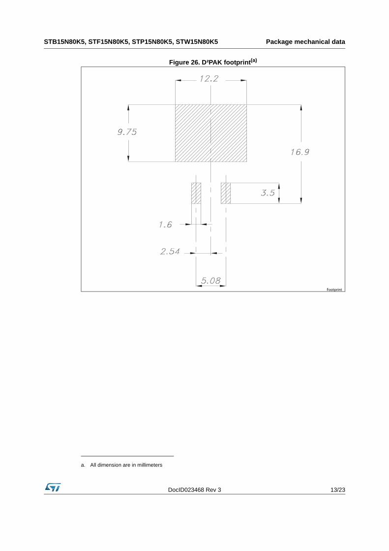
Figure 26. D²PAK footprint(a)
a. All dimension are in millimeters
Footprint
Package mechanical data STB15N80K5, STF15N80K5, STP15N80K5, STW15N80K5
14/23 DocID023468 Rev 3
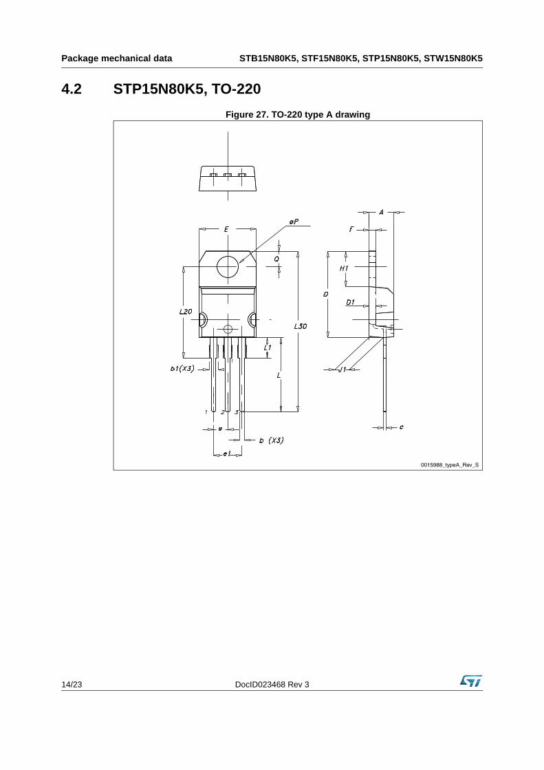
4.2 STP15N80K5, TO-220
Figure 27. TO-220 type A drawing
0015988_typeA_Rev_S
DocID023468 Rev 3 15/23
STB15N80K5, STF15N80K5, STP15N80K5, STW15N80K5 Package mechanical data
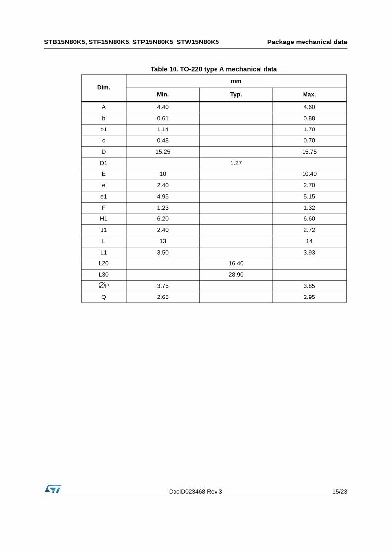
Table 10. TO-220 type A mechanical data
Dim.mm
Min. Typ. Max.
A 4.40 4.60
b 0.61 0.88
b1 1.14 1.70
c 0.48 0.70
D 15.25 15.75
D1 1.27
E 10 10.40
e 2.40 2.70
e1 4.95 5.15
F 1.23 1.32
H1 6.20 6.60
J1 2.40 2.72
L 13 14
L1 3.50 3.93
L20 16.40
L30 28.90
∅P 3.75 3.85
Q 2.65 2.95
Package mechanical data STB15N80K5, STF15N80K5, STP15N80K5, STW15N80K5
16/23 DocID023468 Rev 3
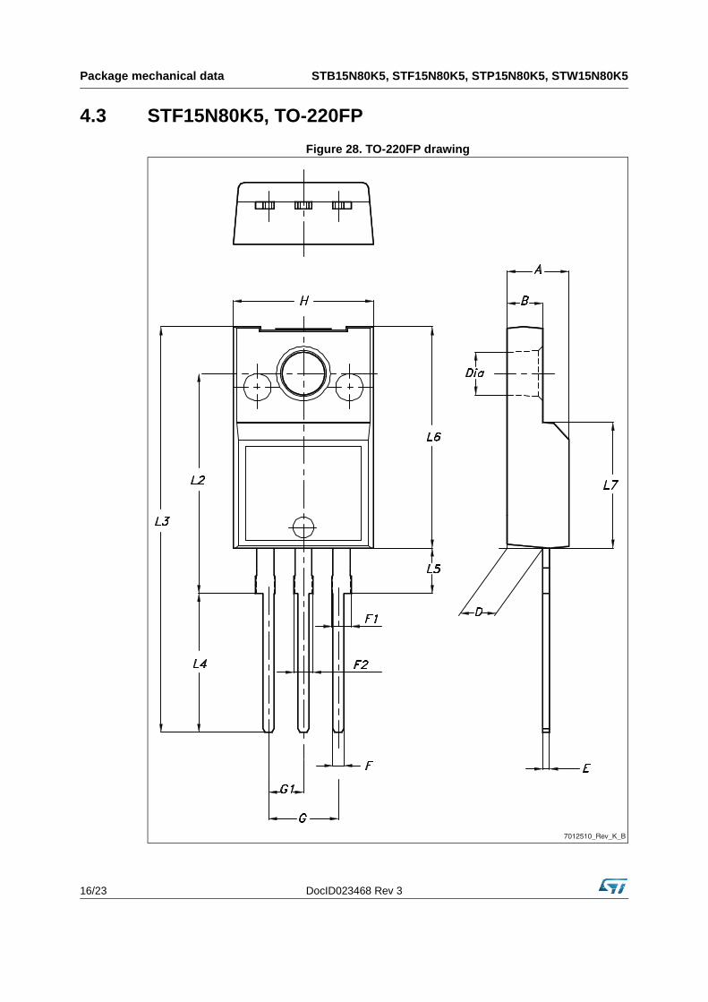
4.3 STF15N80K5, TO-220FP
Figure 28. TO-220FP drawing
7012510_Rev_K_B
DocID023468 Rev 3 17/23
STB15N80K5, STF15N80K5, STP15N80K5, STW15N80K5 Package mechanical data
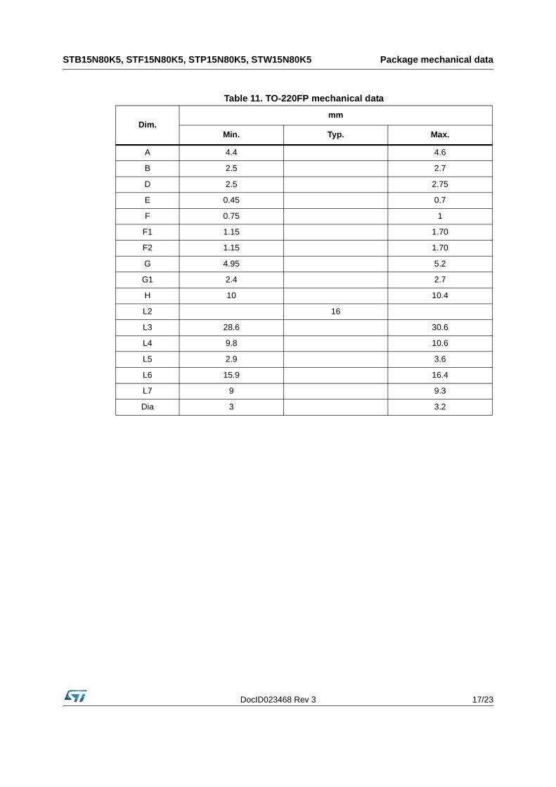
Table 11. TO-220FP mechanical data
Dim.mm
Min. Typ. Max.
A 4.4 4.6
B 2.5 2.7
D 2.5 2.75
E 0.45 0.7
F 0.75 1
F1 1.15 1.70
F2 1.15 1.70
G 4.95 5.2
G1 2.4 2.7
H 10 10.4
L2 16
L3 28.6 30.6
L4 9.8 10.6
L5 2.9 3.6
L6 15.9 16.4
L7 9 9.3
Dia 3 3.2
Package mechanical data STB15N80K5, STF15N80K5, STP15N80K5, STW15N80K5
18/23 DocID023468 Rev 3
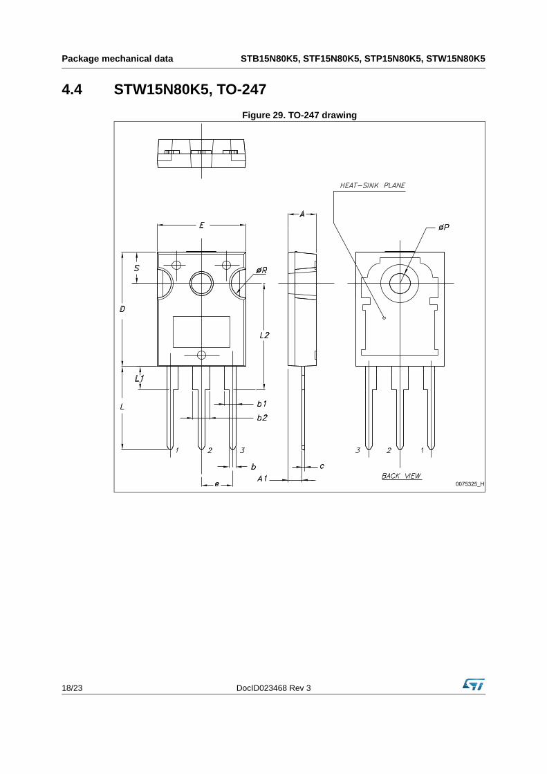
4.4 STW15N80K5, TO-247
Figure 29. TO-247 drawing
0075325_H
DocID023468 Rev 3 19/23
STB15N80K5, STF15N80K5, STP15N80K5, STW15N80K5 Package mechanical data
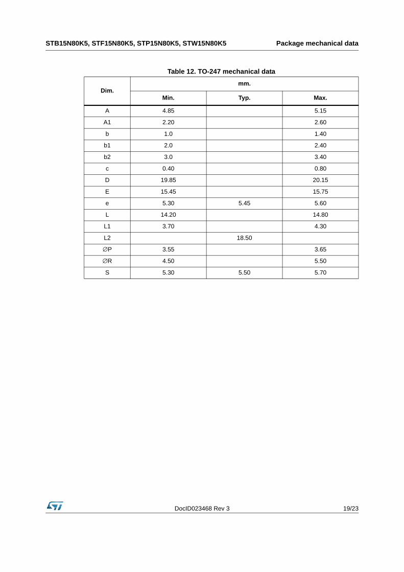
Table 12. TO-247 mechanical data
Dim.mm.
Min. Typ. Max.
A 4.85 5.15
A1 2.20 2.60
b 1.0 1.40
b1 2.0 2.40
b2 3.0 3.40
c 0.40 0.80
D 19.85 20.15
E 15.45 15.75
e 5.30 5.45 5.60
L 14.20 14.80
L1 3.70 4.30
L2 18.50
∅P 3.55 3.65
∅R 4.50 5.50
S 5.30 5.50 5.70
Packaging information STB15N80K5, STF15N80K5, STP15N80K5, STW15N80K5
20/23 DocID023468 Rev 3
5 Packaging information
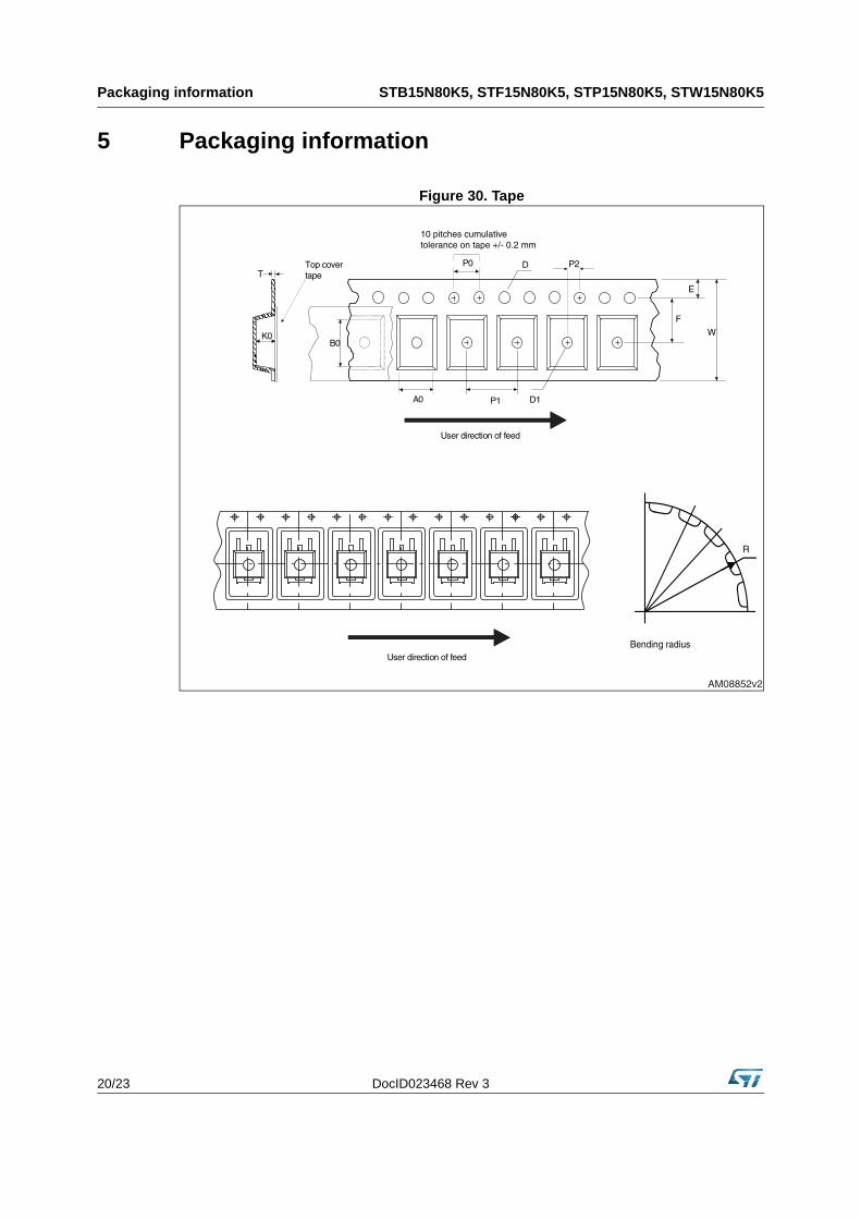
Figure 30. Tape
P1A0 D1
P0
F
W
E
D
B0K0
T
User direction of feed
P2
10 pitches cumulativetolerance on tape +/- 0.2 mm
User direction of feed
R
Bending radius
Top covertape
AM08852v2
DocID023468 Rev 3 21/23
STB15N80K5, STF15N80K5, STP15N80K5, STW15N80K5 Packaging information
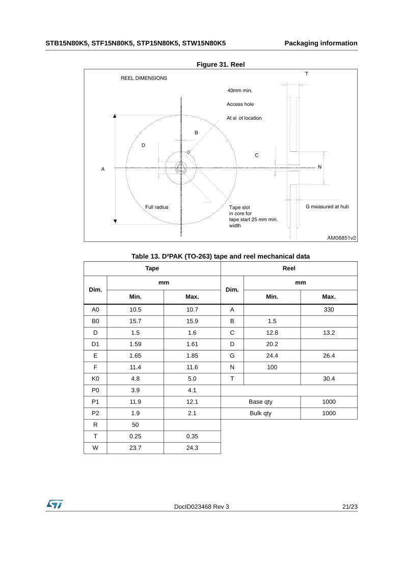
Figure 31. Reel
Table 13. D²PAK (TO-263) tape and reel mechanical data
Tape Reel
Dim.mm
Dim.mm
Min. Max. Min. Max.
A0 10.5 10.7 A 330
B0 15.7 15.9 B 1.5
D 1.5 1.6 C 12.8 13.2
D1 1.59 1.61 D 20.2
E 1.65 1.85 G 24.4 26.4
F 11.4 11.6 N 100
K0 4.8 5.0 T 30.4
P0 3.9 4.1
P1 11.9 12.1 Base qty 1000
P2 1.9 2.1 Bulk qty 1000
R 50
T 0.25 0.35
W 23.7 24.3
A
D
B
Full radius G measured at hub
C
N
REEL DIMENSIONS
40mm min.
Access hole
At sl ot location
T
Tape slot in core fortape start 25 mm min.width
AM08851v2
Revision history STB15N80K5, STF15N80K5, STP15N80K5, STW15N80K5
22/23 DocID023468 Rev 3
6 Revision history
Table 14. Document revision history
Date Revision Changes
18-Jul-2012 1 First release.
31-Oct-2012 2
– Inserted: IAR, EAS and dv/dt values in Table 2– Inserted: Table 5, 6 and 7 typical values– Inserted: Section 2.1: Electrical characteristics (curves)
– Minor text changes
31-Oct-2014 3
Updated title, description and features
Updated Static drain-source on-resistance
Minor text changes
DocID023468 Rev 3 23/23
STB15N80K5, STF15N80K5, STP15N80K5, STW15N80K5
IMPORTANT NOTICE – PLEASE READ CAREFULLY
STMicroelectronics NV and its subsidiaries (“ST”) reserve the right to make changes, corrections, enhancements, modifications, and improvements to ST products and/or to this document at any time without notice. Purchasers should obtain the latest relevant information on ST products before placing orders. ST products are sold pursuant to ST’s terms and conditions of sale in place at the time of order acknowledgement.
Purchasers are solely responsible for the choice, selection, and use of ST products and ST assumes no liability for application assistance or the design of Purchasers’ products.
No license, express or implied, to any intellectual property right is granted by ST herein.
Resale of ST products with provisions different from the information set forth herein shall void any warranty granted by ST for such product.
ST and the ST logo are trademarks of ST. All other product or service names are the property of their respective owners.
Information in this document supersedes and replaces information previously supplied in any prior versions of this document.
© 2014 STMicroelectronics – All rights reserved