N-channel 75 V, 0.018 , 40 A DPAK STripFET II Power · PDF fileDoc ID 9902 Rev 5 7/16 Figure...
16
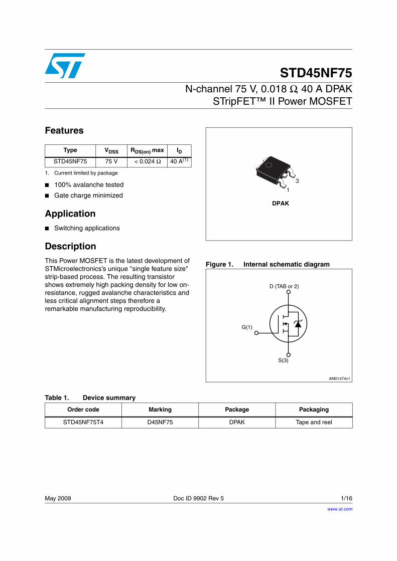
May 2009 Doc ID 9902 Rev 5 1/16 16 STD45NF75 N-channel 75 V, 0.018 Ω , 40 A DPAK STripFET™ II Power MOSFET Features ■ 100% avalanche tested ■ Gate charge minimized Application ■ Switching applications Description This Power MOSFET is the latest development of STMicroelectronics’s unique "single feature size" strip-based process. The resulting transistor shows extremely high packing density for low on- resistance, rugged avalanche characteristics and less critical alignment steps therefore a remarkable manufacturing reproducibility. Figure 1. Internal schematic diagram Type V DSS R DS(on) max I D STD45NF75 75 V < 0.024 Ω 40 A (1) 1. Current limited by package DPAK 1 3 Table 1. Device summary Order code Marking Package Packaging STD45NF75T4 D45NF75 DPAK Tape and reel www.st.com
-
Upload
phungquynh -
Category
Documents
-
view
223 -
download
2
Transcript of N-channel 75 V, 0.018 , 40 A DPAK STripFET II Power · PDF fileDoc ID 9902 Rev 5 7/16 Figure...
May 2009 Doc ID 9902 Rev 5 1/16
16
STD45NF75N-channel 75 V, 0.018 Ω, 40 A DPAK
STripFET™ II Power MOSFET
Features
100% avalanche tested
Gate charge minimized
Application Switching applications
DescriptionThis Power MOSFET is the latest development of STMicroelectronics’s unique "single feature size" strip-based process. The resulting transistor shows extremely high packing density for low on-resistance, rugged avalanche characteristics and less critical alignment steps therefore a remarkable manufacturing reproducibility.
Figure 1. Internal schematic diagram
Type VDSS RDS(on) max ID
STD45NF75 75 V < 0.024 Ω 40 A(1)
1. Current limited by package
DPAK
1
3
Table 1. Device summary
Order code Marking Package Packaging
STD45NF75T4 D45NF75 DPAK Tape and reel
www.st.com
Contents STD45NF75
2/16 Doc ID 9902 Rev 5
Contents
1 Electrical ratings . . . . . . . . . . . . . . . . . . . . . . . . . . . . . . . . . . . . . . . . . . . . 3
2 Electrical characteristics . . . . . . . . . . . . . . . . . . . . . . . . . . . . . . . . . . . . . 4
2.1 Electrical characteristics (curves) . . . . . . . . . . . . . . . . . . . . . . . . . . . . 6
3 Spice thermal model . . . . . . . . . . . . . . . . . . . . . . . . . . . . . . . . . . . . . . . . 10
4 Test circuits . . . . . . . . . . . . . . . . . . . . . . . . . . . . . . . . . . . . . . . . . . . . . 11
5 Package mechanical data . . . . . . . . . . . . . . . . . . . . . . . . . . . . . . . . . . . . 12
6 Packing mechanical data . . . . . . . . . . . . . . . . . . . . . . . . . . . . . . . . . . . . 14
7 Revision history . . . . . . . . . . . . . . . . . . . . . . . . . . . . . . . . . . . . . . . . . . . 15
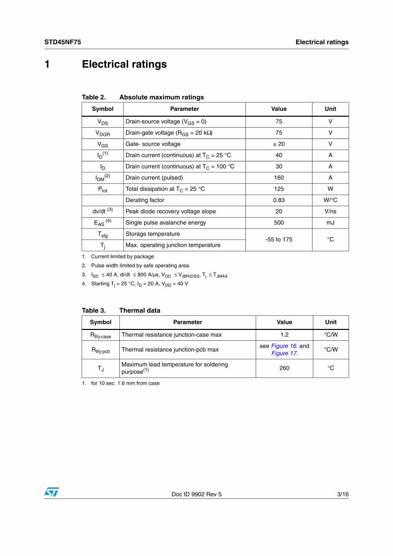
STD45NF75 Electrical ratings
Doc ID 9902 Rev 5 3/16
1 Electrical ratings
Table 2. Absolute maximum ratings
Symbol Parameter Value Unit
VDS Drain-source voltage (VGS = 0) 75 V
VDGR Drain-gate voltage (RGS = 20 kΩ) 75 V
VGS Gate- source voltage ± 20 V
ID(1)
1. Current limited by package
Drain current (continuous) at TC = 25 °C 40 A
ID Drain current (continuous) at TC = 100 °C 30 A
IDM(2)
2. Pulse width limited by safe operating area.
Drain current (pulsed) 160 A
Ptot Total dissipation at TC = 25 °C 125 W
Derating factor 0.83 W/°C
dv/dt (3)
3. ISD ≤ 40 A, di/dt ≤ 800 A/µs, VDD ≤ V(BR)DSS, Tj ≤ TJMAX
Peak diode recovery voltage slope 20 V/ns
EAS (4)
4. Starting Tj = 25 °C, ID = 20 A, VDD = 40 V
Single pulse avalanche energy 500 mJ
Tstg Storage temperature-55 to 175 °C
Tj Max. operating junction temperature
Table 3. Thermal data
Symbol Parameter Value Unit
Rthj-case Thermal resistance junction-case max 1.2 °C/W
Rthj-pcb Thermal resistance junction-pcb max see Figure 16. and
Figure 17. °C/W
TJMaximum lead temperature for soldering purpose(1)
1. for 10 sec. 1.6 mm from case
260 °C
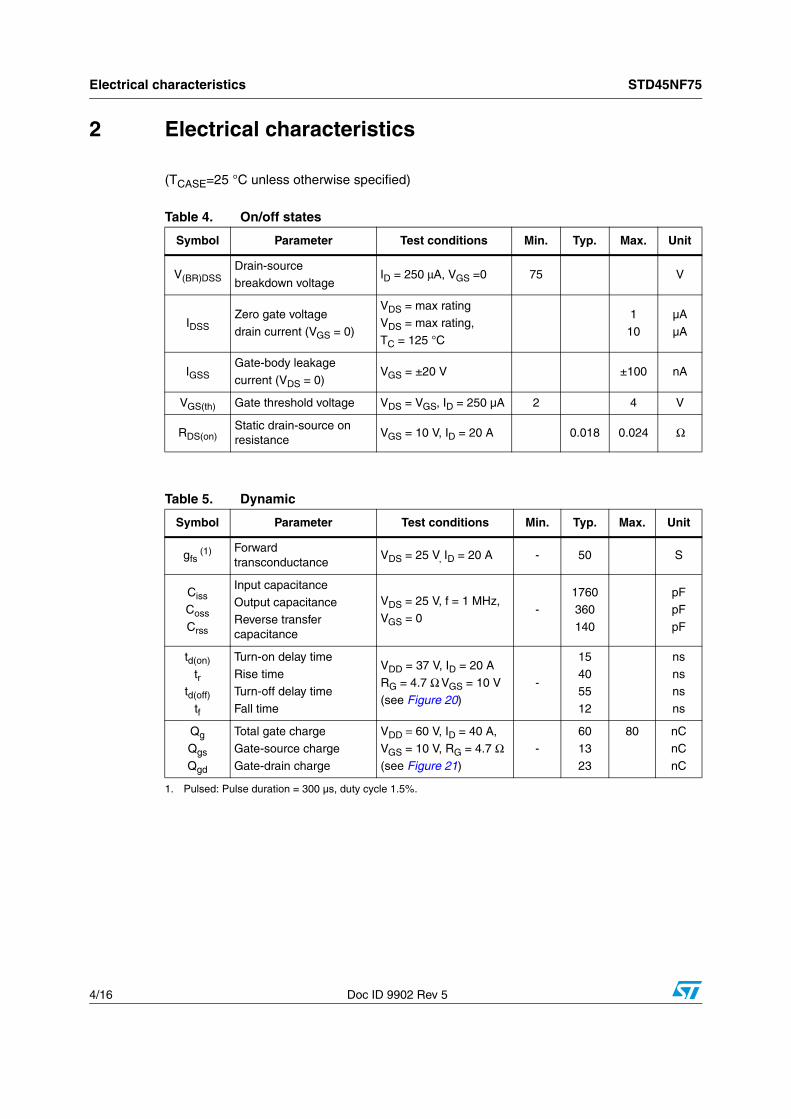
Electrical characteristics STD45NF75
4/16 Doc ID 9902 Rev 5
2 Electrical characteristics
(TCASE=25 °C unless otherwise specified)
Table 4. On/off states
Symbol Parameter Test conditions Min. Typ. Max. Unit
V(BR)DSSDrain-source breakdown voltage
ID = 250 µA, VGS =0 75 V
IDSSZero gate voltage
drain current (VGS = 0)
VDS = max ratingVDS = max rating,
TC = 125 °C
1
10
µA
µA
IGSSGate-body leakage
current (VDS = 0)VGS = ±20 V ±100 nA
VGS(th) Gate threshold voltage VDS = VGS, ID = 250 µA 2 4 V
RDS(on)Static drain-source on resistance
VGS = 10 V, ID = 20 A 0.018 0.024 Ω
Table 5. Dynamic
Symbol Parameter Test conditions Min. Typ. Max. Unit
gfs (1)
1. Pulsed: Pulse duration = 300 µs, duty cycle 1.5%.
Forward transconductance
VDS = 25 V, ID = 20 A - 50 S
Ciss
Coss
Crss
Input capacitance
Output capacitanceReverse transfer capacitance
VDS = 25 V, f = 1 MHz,
VGS = 0-
1760360
140
pFpF
pF
td(on)
trtd(off)
tf
Turn-on delay time
Rise timeTurn-off delay time
Fall time
VDD = 37 V, ID = 20 A
RG = 4.7 Ω VGS = 10 V
(see Figure 20)
-
15
4055
12
ns
nsns
ns
Qg
Qgs
Qgd
Total gate charge
Gate-source charge
Gate-drain charge
VDD = 60 V, ID = 40 A,
VGS = 10 V, RG = 4.7 Ω(see Figure 21)
-
60
13
23
80 nC
nC
nC
STD45NF75 Electrical characteristics
Doc ID 9902 Rev 5 5/16
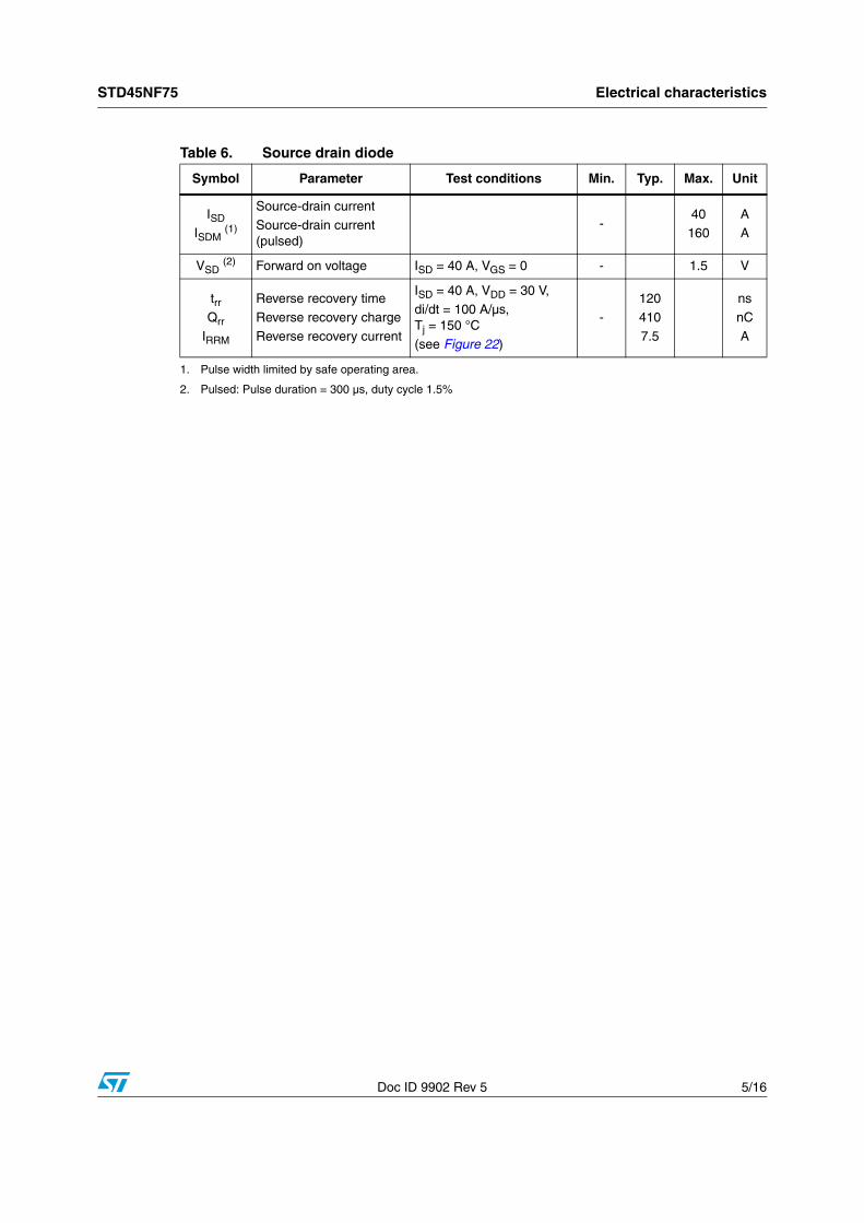
Table 6. Source drain diode
Symbol Parameter Test conditions Min. Typ. Max. Unit
ISD
ISDM (1)
1. Pulse width limited by safe operating area.
Source-drain current
Source-drain current (pulsed)
-40
160AA
VSD (2)
2. Pulsed: Pulse duration = 300 µs, duty cycle 1.5%
Forward on voltage ISD = 40 A, VGS = 0 - 1.5 V
trrQrr
IRRM
Reverse recovery time
Reverse recovery charge
Reverse recovery current
ISD = 40 A, VDD = 30 V,di/dt = 100 A/µs, Tj = 150 °C(see Figure 22)
-
120
410
7.5
ns
nC
A
Electrical characteristics STD45NF75
6/16 Doc ID 9902 Rev 5
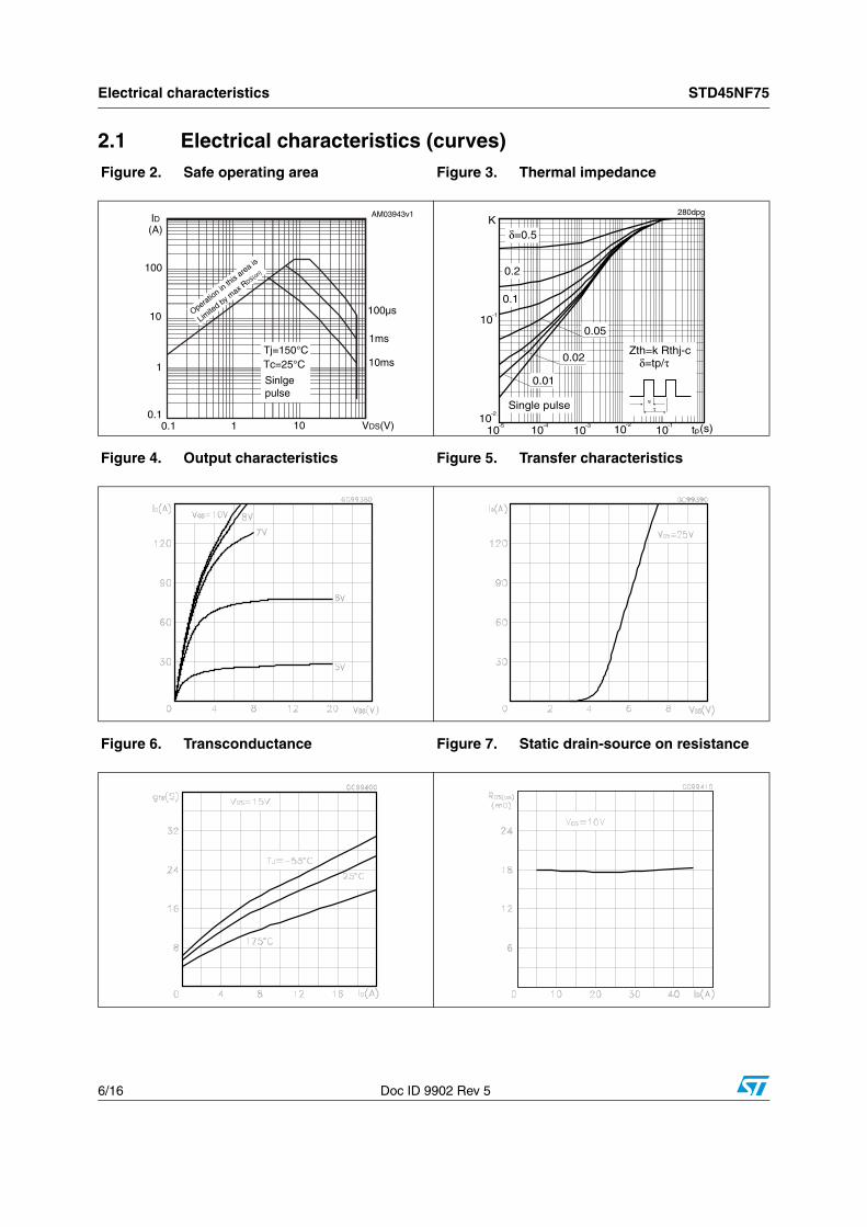
2.1 Electrical characteristics (curves) Figure 2. Safe operating area Figure 3. Thermal impedance
Figure 4. Output characteristics Figure 5. Transfer characteristics
Figure 6. Transconductance Figure 7. Static drain-source on resistance
ID
100
10
1
0.10.1 1 VDS(V)10
(A)
Operation in
this
area is
Limite
d by max R
DS(on)
100µs
1ms
10msTj=150°CTc=25°C
Sinlgepulse
AM03943v1
10-5
10-4
10-3 10
-210
-1tp(s)
10-2
10-1
K
0.2
0.05
0.02
0.01
0.1
Zth=k Rthj-cδ=tp/τ
tp
τSingle pulse
δ=0.5
280dpg
STD45NF75 Electrical characteristics
Doc ID 9902 Rev 5 7/16
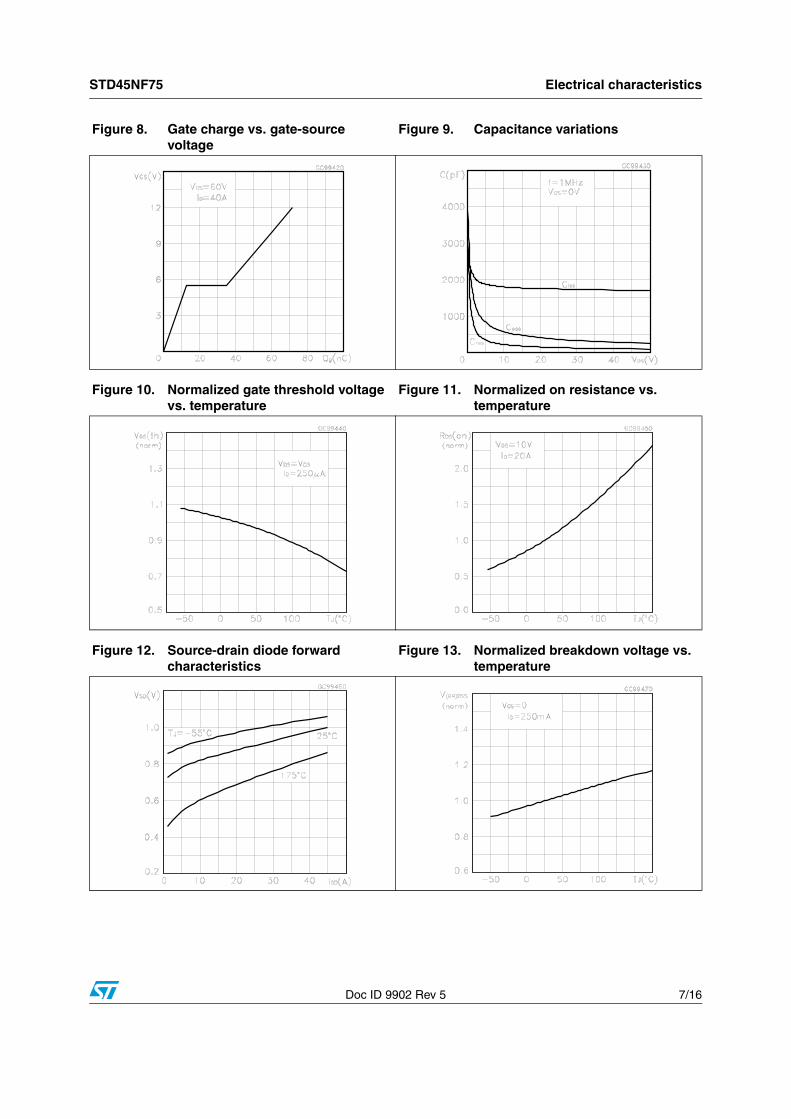
Figure 8. Gate charge vs. gate-source voltage
Figure 9. Capacitance variations
Figure 10. Normalized gate threshold voltage vs. temperature
Figure 11. Normalized on resistance vs. temperature
Figure 12. Source-drain diode forward characteristics
Figure 13. Normalized breakdown voltage vs. temperature
Electrical characteristics STD45NF75
8/16 Doc ID 9902 Rev 5
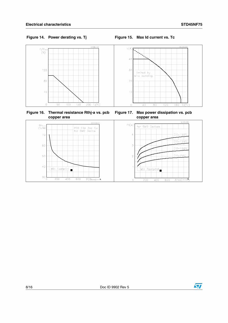
Figure 14. Power derating vs. Tj Figure 15. Max Id current vs. Tc
Figure 16. Thermal resistance Rthj-a vs. pcb copper area
Figure 17. Max power dissipation vs. pcb copper area
STD45NF75 Electrical characteristics
Doc ID 9902 Rev 5 9/16
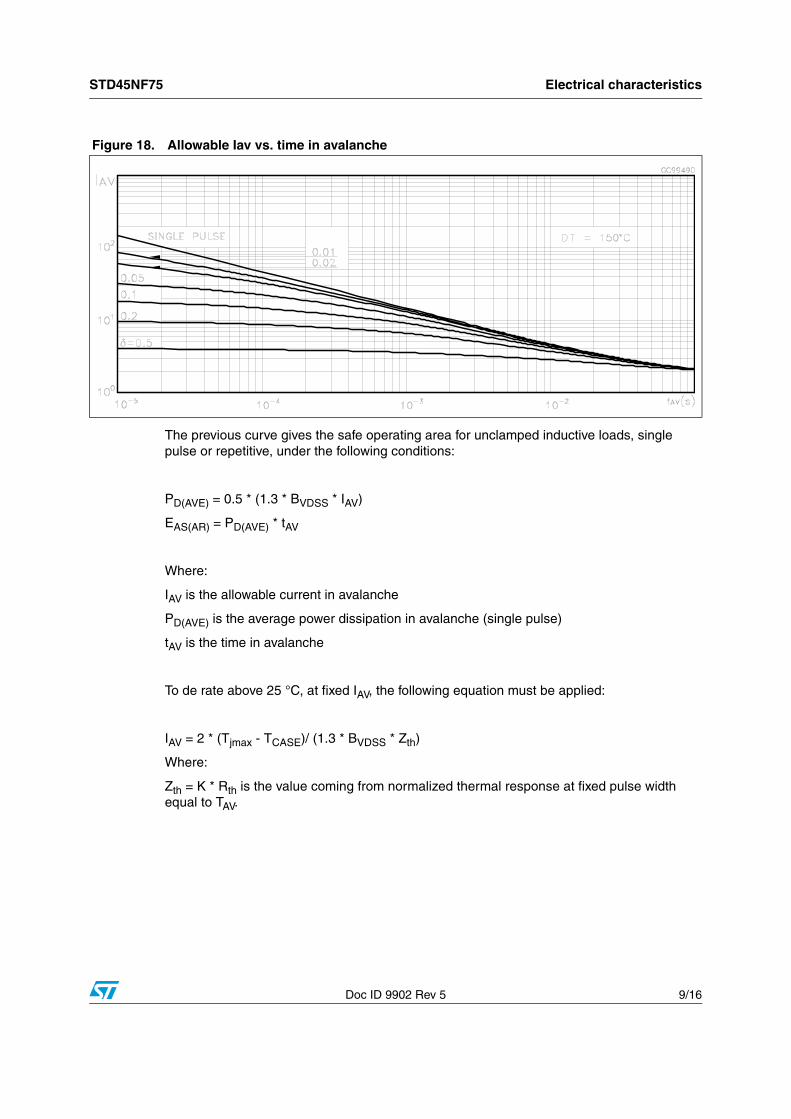
The previous curve gives the safe operating area for unclamped inductive loads, single pulse or repetitive, under the following conditions:
PD(AVE) = 0.5 * (1.3 * BVDSS * IAV)
EAS(AR) = PD(AVE) * tAV
Where:
IAV is the allowable current in avalanche
PD(AVE) is the average power dissipation in avalanche (single pulse)
tAV is the time in avalanche
To de rate above 25 °C, at fixed IAV, the following equation must be applied:
IAV = 2 * (Tjmax - TCASE)/ (1.3 * BVDSS * Zth)
Where:
Zth = K * Rth is the value coming from normalized thermal response at fixed pulse width equal to TAV.
Figure 18. Allowable Iav vs. time in avalanche
Spice thermal model STD45NF75
10/16 Doc ID 9902 Rev 5
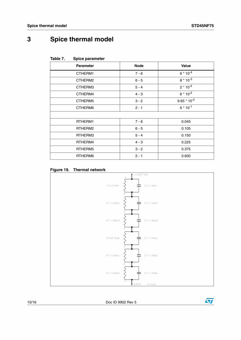
3 Spice thermal model
Figure 19. Thermal network
Table 7. Spice parameter
Parameter Node Value
CTHERM1 7 - 6 6 * 10-4
CTHERM2 6 - 5 8 * 10-3
CTHERM3 5 - 4 2 * 10-2
CTHERM4 4 - 3 6 * 10-2
CTHERM5 3 - 2 9.65 * 10-2
CTHERM6 2 - 1 6 * 10-1
RTHERM1 7 - 6 0.045
RTHERM2 6 - 5 0.105
RTHERM3 5 - 4 0.150
RTHERM4 4 - 3 0.225
RTHERM5 3 - 2 0.375
RTHERM6 2 - 1 0.600
STD45NF75 Test circuits
Doc ID 9902 Rev 5 11/16
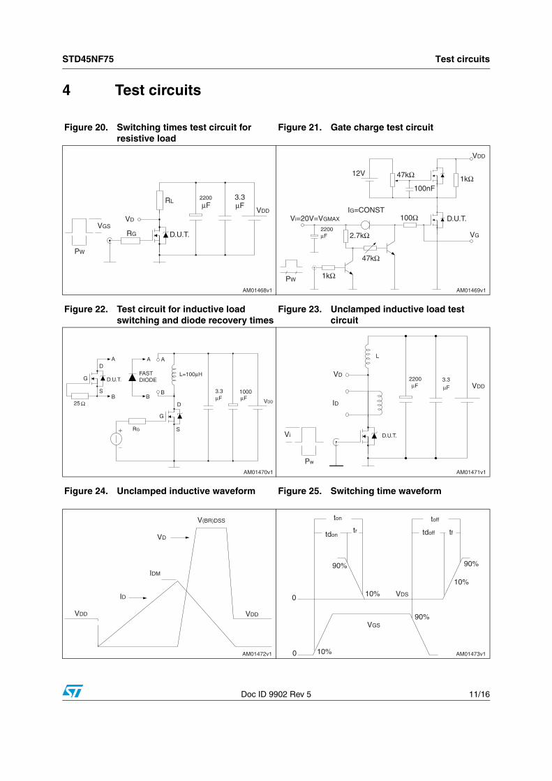
4 Test circuits
Figure 20. Switching times test circuit for resistive load
Figure 21. Gate charge test circuit
Figure 22. Test circuit for inductive load switching and diode recovery times
Figure 23. Unclamped inductive load test circuit
Figure 24. Unclamped inductive waveform Figure 25. Switching time waveform
AM01468v1
VGS
PW
VD
RG
RL
D.U.T.
2200
µF3.3µF
VDD
AM01469v1
VDD
47kΩ 1kΩ
47kΩ
2.7kΩ
1kΩ
12V
Vi=20V=VGMAX
2200µF
PW
IG=CONST100Ω
100nF
D.U.T.
VG
AM01470v1
AD
D.U.T.
SB
G
25 Ω
A A
BB
RG
G
FASTDIODE
D
S
L=100µH
µF3.3 1000
µF VDD
AM01471v1
Vi
Pw
VD
ID
D.U.T.
L
2200µF
3.3µF VDD
AM01472v1
V(BR)DSS
VDDVDD
VD
IDM
ID
AM01473v1
VDS
ton
tdon tdoff
toff
tftr
90%
10%
10%
0
0
90%
90%
10%
VGS
Package mechanical data STD45NF75
12/16 Doc ID 9902 Rev 5
5 Package mechanical data
In order to meet environmental requirements, ST offers these devices in different grades of ECOPACK® packages, depending on their level of environmental compliance. ECOPACK® specifications, grade definitions and product status are available at: www.st.com. ECOPACK is an ST trademark.
STD45NF75 Package mechanical data
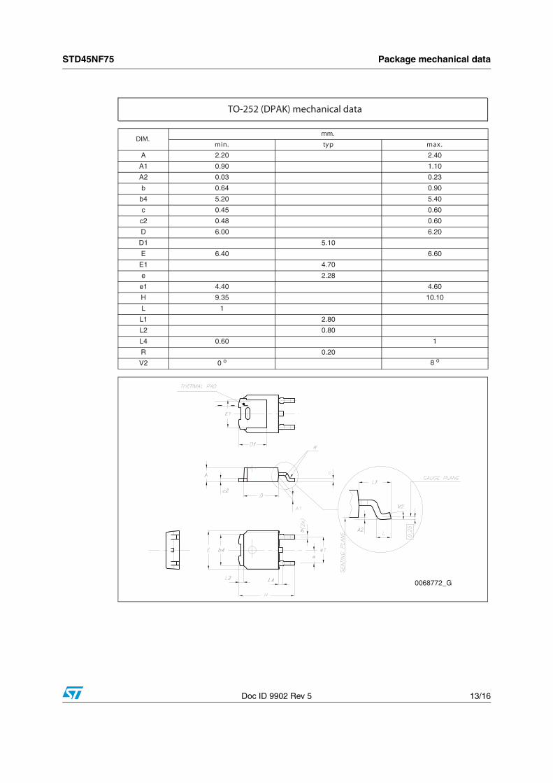
Doc ID 9902 Rev 5 13/16
DIM.mm.
.xampyt.nim
04.202.2A
01.109.01A
32.030.02A
09.046.0b
04.502.54b
06.054.0c
06.084.02c
02.600.6D
01.51D
06.604.6E
07.41E
82.2e
06.404.41e
01.0153.9H
1L
08.21L
08.02L
106.04L
02.0R
V2 0 o 8 o
TO-252 (DPAK) mechanical data
0068772_G
Packing mechanical data STD45NF75
14/16 Doc ID 9902 Rev 5
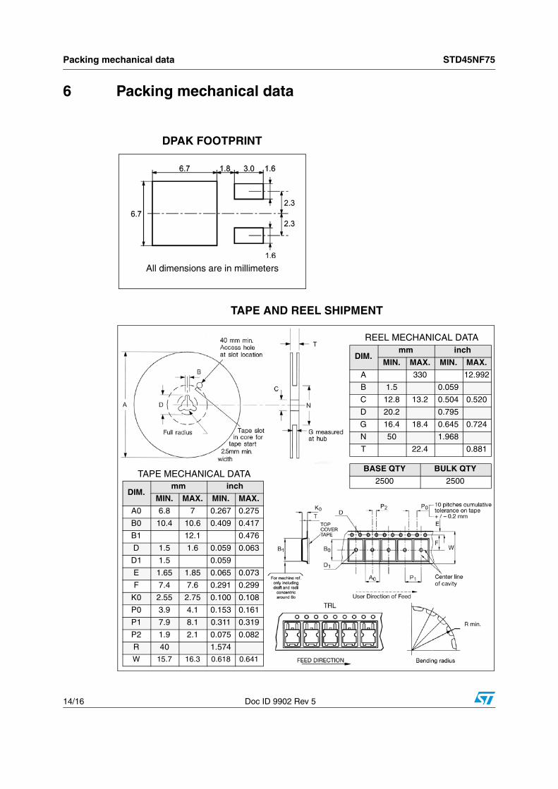
6 Packing mechanical data
TAPE AND REEL SHIPMENT
DPAK FOOTPRINT
DIM.mm inch
MIN. MAX. MIN. MAX.
A 330 12.992
B 1.5 0.059
C 12.8 13.2 0.504 0.520
D 20.2 0.795
G 16.4 18.4 0.645 0.724
N 50 1.968
T 22.4 0.881
BASE QTY BULK QTY
2500 2500
REEL MECHANICAL DATA
DIM.mm inch
MIN. MAX. MIN. MAX.
A0 6.8 7 0.267 0.275
B0 10.4 10.6 0.409 0.417
B1 12.1 0.476
D 1.5 1.6 0.059 0.063
D1 1.5 0.059
E 1.65 1.85 0.065 0.073
F 7.4 7.6 0.291 0.299
K0 2.55 2.75 0.100 0.108
P0 3.9 4.1 0.153 0.161
P1 7.9 8.1 0.311 0.319
P2 1.9 2.1 0.075 0.082
R 40 1.574
W 15.7 16.3 0.618 0.641
TAPE MECHANICAL DATA
All dimensions are in millimeters
STD45NF75 Revision history
Doc ID 9902 Rev 5 15/16
7 Revision history
Table 8. Document revision history
Date Revision Changes
22-Jun-2004 1 Preliminary version
09-Sep-2004 2 Complete version
11-Jul-2006 3 New template, no content change
20-Feb-2007 4 Typo mistake on page 1
20-May-2009 5 Figure 2 and Figure 3 have been updated
STD45NF75
16/16 Doc ID 9902 Rev 5
Please Read Carefully:
Information in this document is provided solely in connection with ST products. STMicroelectronics NV and its subsidiaries (“ST”) reserve theright to make changes, corrections, modifications or improvements, to this document, and the products and services described herein at anytime, without notice.
All ST products are sold pursuant to ST’s terms and conditions of sale.
Purchasers are solely responsible for the choice, selection and use of the ST products and services described herein, and ST assumes noliability whatsoever relating to the choice, selection or use of the ST products and services described herein.
No license, express or implied, by estoppel or otherwise, to any intellectual property rights is granted under this document. If any part of thisdocument refers to any third party products or services it shall not be deemed a license grant by ST for the use of such third party productsor services, or any intellectual property contained therein or considered as a warranty covering the use in any manner whatsoever of suchthird party products or services or any intellectual property contained therein.
UNLESS OTHERWISE SET FORTH IN ST’S TERMS AND CONDITIONS OF SALE ST DISCLAIMS ANY EXPRESS OR IMPLIEDWARRANTY WITH RESPECT TO THE USE AND/OR SALE OF ST PRODUCTS INCLUDING WITHOUT LIMITATION IMPLIEDWARRANTIES OF MERCHANTABILITY, FITNESS FOR A PARTICULAR PURPOSE (AND THEIR EQUIVALENTS UNDER THE LAWSOF ANY JURISDICTION), OR INFRINGEMENT OF ANY PATENT, COPYRIGHT OR OTHER INTELLECTUAL PROPERTY RIGHT.
UNLESS EXPRESSLY APPROVED IN WRITING BY AN AUTHORIZED ST REPRESENTATIVE, ST PRODUCTS ARE NOTRECOMMENDED, AUTHORIZED OR WARRANTED FOR USE IN MILITARY, AIR CRAFT, SPACE, LIFE SAVING, OR LIFE SUSTAININGAPPLICATIONS, NOR IN PRODUCTS OR SYSTEMS WHERE FAILURE OR MALFUNCTION MAY RESULT IN PERSONAL INJURY,DEATH, OR SEVERE PROPERTY OR ENVIRONMENTAL DAMAGE. ST PRODUCTS WHICH ARE NOT SPECIFIED AS "AUTOMOTIVEGRADE" MAY ONLY BE USED IN AUTOMOTIVE APPLICATIONS AT USER’S OWN RISK.
Resale of ST products with provisions different from the statements and/or technical features set forth in this document shall immediately voidany warranty granted by ST for the ST product or service described herein and shall not create or extend in any manner whatsoever, anyliability of ST.
ST and the ST logo are trademarks or registered trademarks of ST in various countries.
Information in this document supersedes and replaces all information previously supplied.
The ST logo is a registered trademark of STMicroelectronics. All other names are the property of their respective owners.
© 2009 STMicroelectronics - All rights reserved
STMicroelectronics group of companies
Australia - Belgium - Brazil - Canada - China - Czech Republic - Finland - France - Germany - Hong Kong - India - Israel - Italy - Japan - Malaysia - Malta - Morocco - Philippines - Singapore - Spain - Sweden - Switzerland - United Kingdom - United States of America
www.st.com