
N-channel 650 V, 35 A, 0.067 typ., MDmesh V Power … · This is information on a product in full...
18
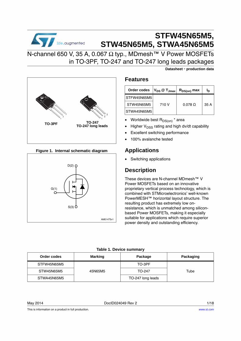
This is information on a product in full production. May 2014 DocID024049 Rev 2 1/18 STFW45N65M5, STW45N65M5, STWA45N65M5 N-channel 650 V, 35 A, 0.067 Ω typ., MDmesh™ V Power MOSFETs in TO-3PF, TO-247 and TO-247 long leads packages Datasheet - production data Figure 1. Internal schematic diagram Features • Worldwide best R DS(on) * area • Higher V DSS rating and high dv/dt capability • Excellent switching performance • 100% avalanche tested Applications • Switching applications Description These devices are N-channel MDmesh™ V Power MOSFETs based on an innovative proprietary vertical process technology, which is combined with STMicroelectronics’ well-known PowerMESH™ horizontal layout structure. The resulting product has extremely low on- resistance, which is unmatched among silicon- based Power MOSFETs, making it especially suitable for applications which require superior power density and outstanding efficiency. TO-247 1 2 3 TO-247 long leads 1 1 2 3 TO-3PF Order codes V DS @ T Jmax R DS(on) max I D STFW45N65M5 710 V 0.078 Ω 35 A STW45N65M5 STWA45N65M5 Table 1. Device summary Order codes Marking Package Packaging STFW45N65M5 45N65M5 TO-3PF Tube STW45N65M5 TO-247 STWA45N65M5 TO-247 long leads www.st.com
-
Upload
phamnguyet -
Category
Documents
-
view
218 -
download
0
Transcript of N-channel 650 V, 35 A, 0.067 typ., MDmesh V Power … · This is information on a product in full...
This is information on a product in full production.
May 2014 DocID024049 Rev 2 1/18
STFW45N65M5, STW45N65M5, STWA45N65M5
N-channel 650 V, 35 A, 0.067 Ω typ., MDmesh™ V Power MOSFETs
in TO-3PF, TO-247 and TO-247 long leads packages
Datasheet - production data
Figure 1. Internal schematic diagram
Features
• Worldwide best RDS(on)
* area
• Higher VDSS
rating and high dv/dt capability
• Excellent switching performance
• 100% avalanche tested
Applications• Switching applications
DescriptionThese devices are N-channel MDmesh™ V
Power MOSFETs based on an innovative
proprietary vertical process technology, which is
combined with STMicroelectronics’ well-known
PowerMESH™ horizontal layout structure. The
resulting product has extremely low on-
resistance, which is unmatched among silicon-
based Power MOSFETs, making it especially
suitable for applications which require superior
power density and outstanding efficiency.
TO-2471
2
3
TO-247 long leads
111
123
TO-3PF
Order codes VDS @ TJmax RDS(on) max ID
STFW45N65M5
710 V 0.078 Ω 35 ASTW45N65M5
STWA45N65M5
Table 1. Device summary
Order codes Marking Package Packaging
STFW45N65M5
45N65M5
TO-3PF
TubeSTW45N65M5 TO-247
STWA45N65M5 TO-247 long leads
www.st.com
Contents STFW45N65M5, STW45N65M5, STWA45N65M5
2/18 DocID024049 Rev 2
Contents
1 Electrical ratings . . . . . . . . . . . . . . . . . . . . . . . . . . . . . . . . . . . . . . . . . . . . 3
2 Electrical characteristics . . . . . . . . . . . . . . . . . . . . . . . . . . . . . . . . . . . . . 4
2.1 Electrical characteristics (curves) . . . . . . . . . . . . . . . . . . . . . . . . . . . . . . . 6
3 Test circuits . . . . . . . . . . . . . . . . . . . . . . . . . . . . . . . . . . . . . . . . . . . . . . 9
4 Package mechanical data . . . . . . . . . . . . . . . . . . . . . . . . . . . . . . . . . . . . 10
4.1 TO-3PF, STFW45N65M5 . . . . . . . . . . . . . . . . . . . . . . . . . . . . . . . . . . . . . .11
4.2 TO-247, STW45N65M5 . . . . . . . . . . . . . . . . . . . . . . . . . . . . . . . . . . . . . . 13
4.3 TO-247 long leads, STWA45N65M5 . . . . . . . . . . . . . . . . . . . . . . . . . . . . 15
5 Revision history . . . . . . . . . . . . . . . . . . . . . . . . . . . . . . . . . . . . . . . . . . . 17
DocID024049 Rev 2 3/18
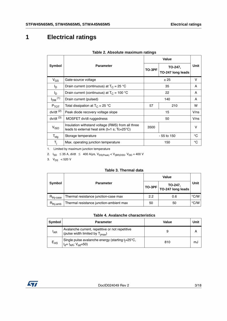
STFW45N65M5, STW45N65M5, STWA45N65M5 Electrical ratings
18
1 Electrical ratings
Table 2. Absolute maximum ratings
Symbol Parameter
Value
UnitTO-3PF
TO-247,
TO-247 long leads
VGS
Gate-source voltage ± 25 V
ID
Drain current (continuous) at TC
= 25 °C 35 A
ID
Drain current (continuous) at TC
= 100 °C 22 A
IDM
(1)
1. Limited by maximum junction temperature
Drain current (pulsed) 140 A
PTOT
Total dissipation at TC
= 25 °C 57 210 W
dv/dt (2)
2. ISD
≤ 35 A, di/dt ≤ 400 A/μs, VDS(Peak)
< V(BR)DSS
, VDD
= 400 V
Peak diode recovery voltage slope 15 V/ns
dv/dt (3)
3. VDS
< 520 V
MOSFET dv/dt ruggedness 50 V/ns
VISO
Insulation withstand voltage (RMS) from all three
leads to external heat sink (t=1 s; Tc=25°C)
3500 V
Tstg
Storage temperature - 55 to 150 °C
Tj
Max. operating junction temperature 150 °C
Table 3. Thermal data
Symbol Parameter
Value
UnitTO-3PF
TO-247, TO-247 long leads
Rthj-case
Thermal resistance junction-case max 2.2 0.6 °C/W
Rthj-amb
Thermal resistance junction-ambient max 50 50 °C/W
Table 4. Avalanche characteristics
Symbol Parameter Value Unit
IAR
Avalanche current, repetitive or not repetitive
(pulse width limited by Tjmax
)
9 A
EAS
Single pulse avalanche energy (starting tj=25°C,
Id= I
AR; V
dd=50)
810 mJ
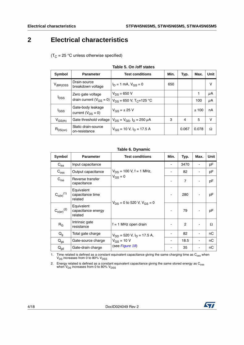
Electrical characteristics STFW45N65M5, STW45N65M5, STWA45N65M5
4/18 DocID024049 Rev 2
2 Electrical characteristics
(TC
= 25 °C unless otherwise specified)
Table 5. On /off states
Symbol Parameter Test conditions Min. Typ. Max. Unit
V(BR)DSS
Drain-source
breakdown voltage
ID
= 1 mA, VGS
= 0 650 V
IDSS
Zero gate voltage
drain current (VGS
= 0)
VDS
= 650 V 1 μA
VDS
= 650 V, TC
=125 °C 100 μA
IGSS
Gate-body leakage
current (VDS
= 0)
VGS
= ± 25 V ± 100 nA
VGS(th)
Gate threshold voltage VDS
= VGS
, ID
= 250 μA 3 4 5 V
RDS(on)
Static drain-source
on-resistance
VGS
= 10 V, ID
= 17.5 A 0.067 0.078 Ω
Table 6. Dynamic
Symbol Parameter Test conditions Min. Typ. Max. Unit
Ciss
Input capacitance
VDS
= 100 V, f = 1 MHz,
VGS
= 0
- 3470 - pF
Coss Output capacitance - 82 - pF
Crss
Reverse transfer
capacitance- 7 - pF
Co(tr)
(1)
1. Time related is defined as a constant equivalent capacitance giving the same charging time as Coss
when
VDS
increases from 0 to 80% VDSS
Equivalent
capacitance time
related
VDS
= 0 to 520 V, VGS
= 0
- 280 - pF
Co(er)
(2)
2. Energy related is defined as a constant equivalent capacitance giving the same stored energy as Coss
when VDS
increases from 0 to 80% VDSS
Equivalent
capacitance energy
related
- 79 - pF
RG
Intrinsic gate
resistance
f = 1 MHz open drain - 2 - Ω
Qg
Total gate chargeV
DD = 520 V, I
D = 17.5 A,
VGS
= 10 V
(see Figure 18)
- 82 - nC
Qgs
Gate-source charge - 18.5 - nC
Qgd
Gate-drain charge - 35 - nC
DocID024049 Rev 2 5/18
STFW45N65M5, STW45N65M5, STWA45N65M5 Electrical characteristics
18
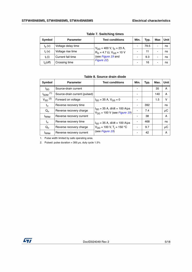
Table 7. Switching times
Symbol Parameter Test conditions Min. Typ. Max Unit
td (v) Voltage delay time
VDD
= 400 V, ID
= 23 A,
RG
= 4.7 Ω, VGS
= 10 V
(see Figure 19 and
Figure 22)
- 79.5 - ns
tr (v) Voltage rise time - 11 - ns
tf (i) Current fall time - 9.3 - ns
tc(off) Crossing time - 16 - ns
Table 8. Source drain diode
Symbol Parameter Test conditions Min. Typ. Max. Unit
ISD
Source-drain current - 35 A
ISDM
(1)
1. Pulse width limited by safe operating area.
Source-drain current (pulsed) - 140 A
VSD
(2)
2. Pulsed: pulse duration = 300 μs, duty cycle 1.5%
Forward on voltage ISD
= 35 A, VGS
= 0 - 1.5 V
trr
Reverse recovery time
ISD
= 35 A, di/dt = 100 A/μs
VDD
= 100 V (see Figure 19)
- 392 ns
Qrr
Reverse recovery charge - 7.4 μC
IRRM
Reverse recovery current - 38 A
trr
Reverse recovery timeISD
= 35 A, di/dt = 100 A/μs
VDD
= 100 V, Tj = 150 °C
(see Figure 19)
- 468 ns
Qrr
Reverse recovery charge - 9.7 μC
IRRM
Reverse recovery current - 42 A
Electrical characteristics STFW45N65M5, STW45N65M5, STWA45N65M5
6/18 DocID024049 Rev 2
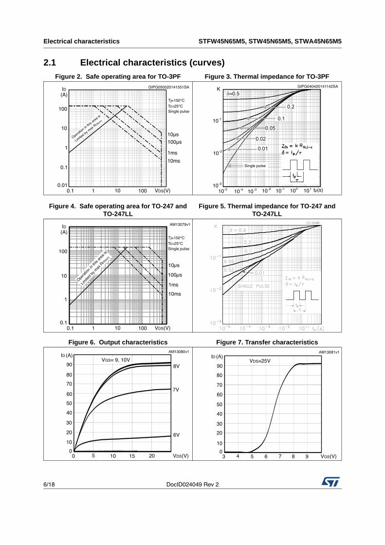
2.1 Electrical characteristics (curves)
Figure 2. Safe operating area for TO-3PF Figure 3. Thermal impedance for TO-3PF
Single pulse
δ=0.5
0.05
0.02
0.01
0.1
0.2
K
10 tp(s)-4 10-310-3
10-2
10-5 10-2 10-1 100
c
10-1
101
GIPG040420141142SA
Figure 4. Safe operating area for TO-247 and TO-247LL
Figure 5. Thermal impedance for TO-247 and TO-247LL
Figure 6. Output characteristics Figure 7. Transfer characteristics
ID
100
10
1
0.10.1 1 100 VDS(V)10
(A)
Opera
tion
in th
is ar
ea is
Limite
d by
max
RDS(o
n)
10µs
100µs
1ms
10ms
Tj=150°C
Tc=25°CSingle pulse
AM13079v1
ID
60
40
20
00 10 VDS(V)20
(A)
5 15
80
6V
VGS= 9, 10V
10
30
50
707V
90 8V
AM13080v1ID
60
40
20
03 5 VGS(V)7
(A)
4 6 8
80
9
10
30
50
70
VDS=25V90
AM13081v1
DocID024049 Rev 2 7/18
STFW45N65M5, STW45N65M5, STWA45N65M5 Electrical characteristics
18
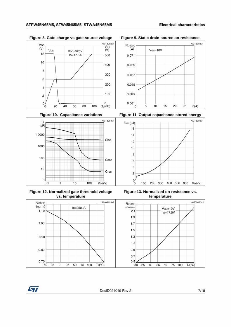
Figure 8. Gate charge vs gate-source voltage Figure 9. Static drain-source on-resistance
Figure 10. Capacitance variations Figure 11. Output capacitance stored energy
Figure 12. Normalized gate threshold voltage vs. temperature
Figure 13. Normalized on-resistance vs. temperature
VGS
6
4
2
00 20 Qg(nC)
(V)
80
8
40 60
10
VDD=520VID=17.5A
100
12
300
200
100
0
400
500
VDS
VDS(V)
AM13082v1RDS(on)
0.067
0.065
0.063
0.0610 15 ID(A)
(Ω)
10 20
0.069
0.071
VGS=10V
255
AM13083v1
C
1000
100
10
10.1 10 VDS(V)
(pF)
1
10000
100
Ciss
Coss
Crss
AM13084v1Eoss
6
4
2
00 100 VDS(V)
(µJ)
400
8
200 300
10
12
500 600
14
16
AM13085v1
VGS(th)
1.00
0.90
0.80
0.70-50 0 TJ(°C)
(norm)
-25
1.10
7525 50 100
ID=250µA
AM05459v2 RDS(on)
1.7
1.3
0.9
0.5-50 0 TJ(°C)
(norm)
-25 7525 50 100
0.7
1.1
1.5
1.9
2.1VGS=10VID=17.5V
AM05460v2
Electrical characteristics STFW45N65M5, STW45N65M5, STWA45N65M5
8/18 DocID024049 Rev 2
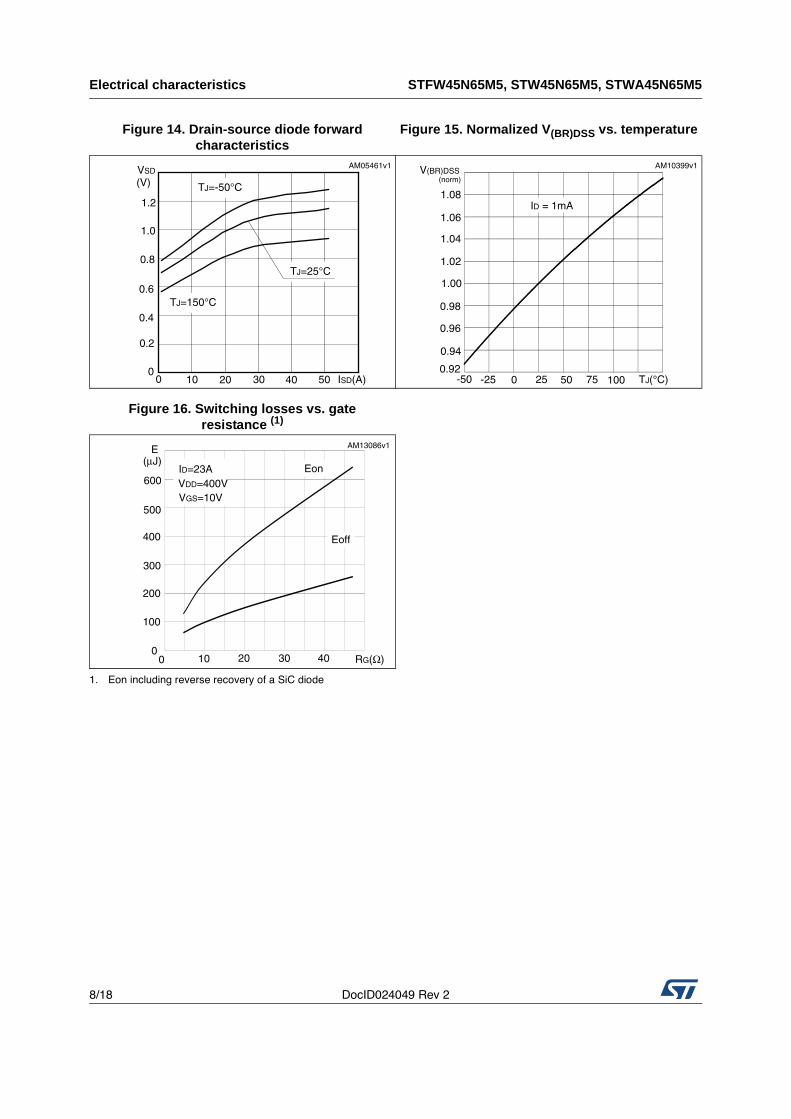
Figure 14. Drain-source diode forward characteristics
Figure 15. Normalized V(BR)DSS vs. temperature
Figure 16. Switching losses vs. gate resistance (1)
1. Eon including reverse recovery of a SiC diode
VSD
0 20 ISD(A)
(V)
10 5030 400
0.2
0.4
0.6
0.8
1.0
1.2
TJ=-50°C
TJ=150°C
TJ=25°C
AM05461v1 V(BR)DSS
-50 0 TJ(°C)
(norm)
-25 7525 50 1000.92
0.94
0.96
0.98
1.00
1.04
1.06
1.02
ID = 1mA1.08
AM10399v1
E
300
200
100
00 20 RG(Ω)
(μJ)
10 30
400
500
600
40
ID=23AVDD=400V
Eon
Eoff
VGS=10V
AM13086v1
DocID024049 Rev 2 9/18
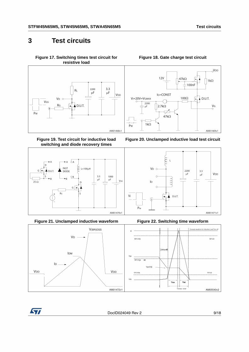
STFW45N65M5, STW45N65M5, STWA45N65M5 Test circuits
18
3 Test circuits
Figure 17. Switching times test circuit for resistive load
Figure 18. Gate charge test circuit
Figure 19. Test circuit for inductive load switching and diode recovery times
Figure 20. Unclamped inductive load test circuit
Figure 21. Unclamped inductive waveform Figure 22. Switching time waveform
AM01468v1
VGS
PW
VD
RG
RL
D.U.T.
2200
μF3.3μF
VDD
AM01469v1
VDD
47kΩ 1kΩ
47kΩ
2.7kΩ
1kΩ
12V
Vi=20V=VGMAX
2200μF
PW
IG=CONST100Ω
100nF
D.U.T.
VG
AM01470v1
AD
D.U.T.
SB
G
25 Ω
A A
BB
RG
G
FASTDIODE
D
S
L=100μH
μF3.3 1000
μF VDD
AM01471v1
Vi
Pw
VD
ID
D.U.T.
L
2200μF
3.3μF VDD
AM01472v1
V(BR)DSS
VDDVDD
VD
IDM
ID
AM05540v2
Id
Vgs
Vds
90%Vds
10%Id
90%Vgs on
Tdelay-off
TfallTrise
Tcross -over
10%Vds
90%Id
Vgs(I(t))
on
-off
TfallTrise
-
))
Concept waveform for Inductive Load Turn-off
Package mechanical data STFW45N65M5, STW45N65M5, STWA45N65M5
10/18 DocID024049 Rev 2
4 Package mechanical data
In order to meet environmental requirements, ST offers these devices in different grades of
ECOPACK®
packages, depending on their level of environmental compliance. ECOPACK®
specifications, grade definitions and product status are available at: www.st.com.
ECOPACK is an ST trademark.
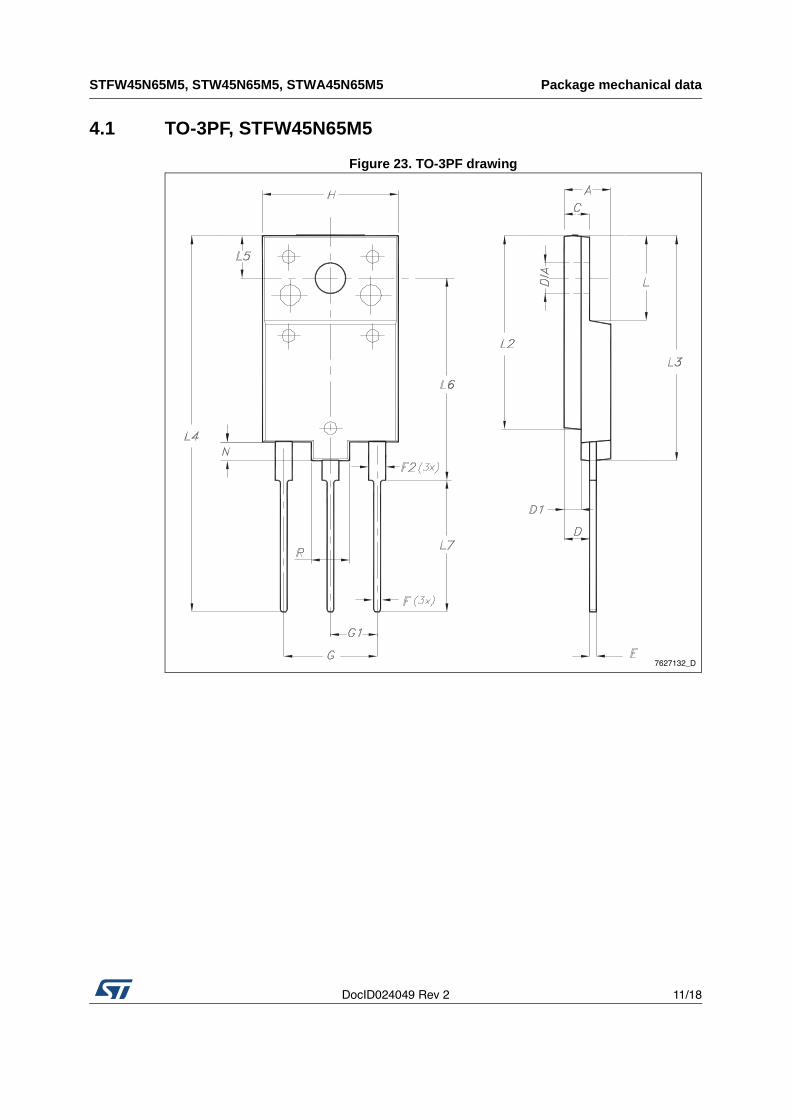
DocID024049 Rev 2 11/18
STFW45N65M5, STW45N65M5, STWA45N65M5 Package mechanical data
18
4.1 TO-3PF, STFW45N65M5
Figure 23. TO-3PF drawing
7627132_D
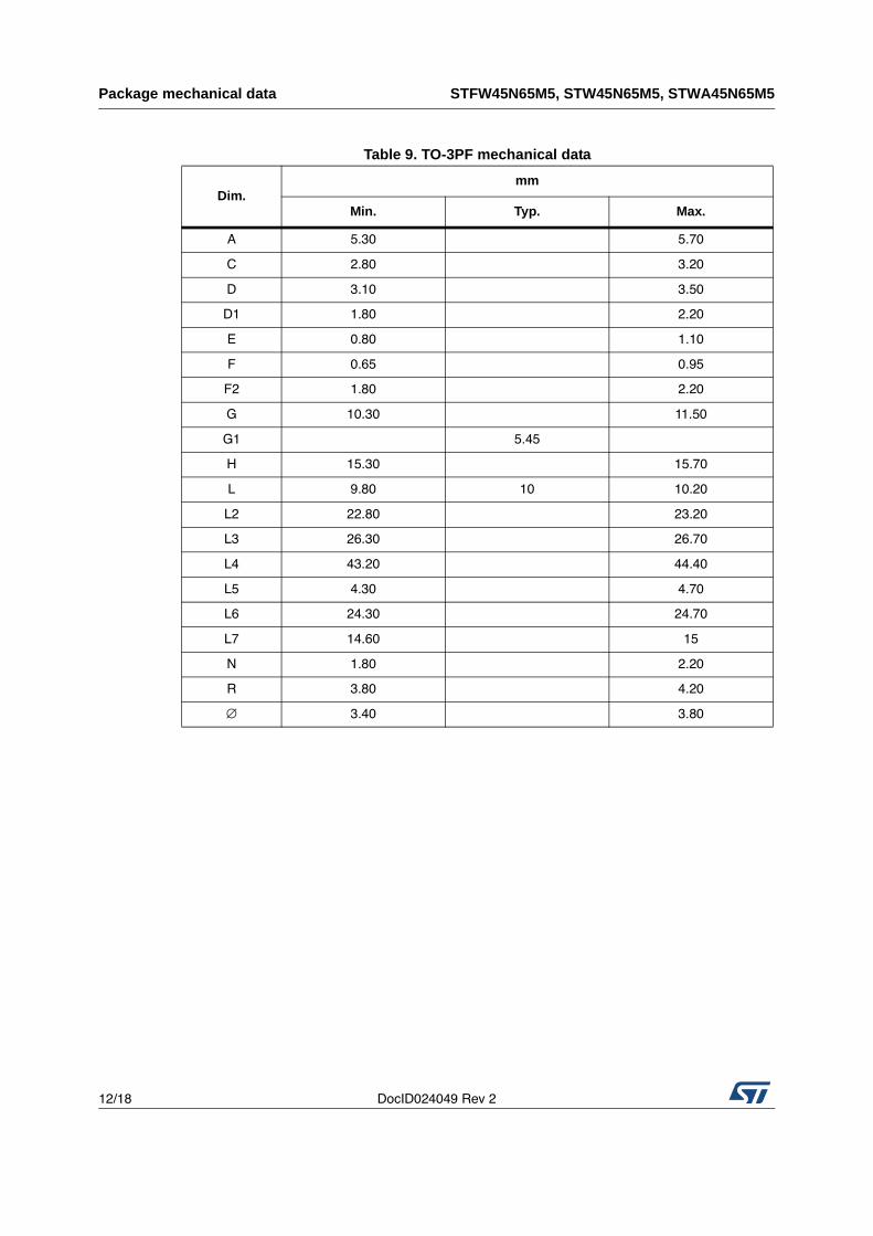
Package mechanical data STFW45N65M5, STW45N65M5, STWA45N65M5
12/18 DocID024049 Rev 2
Table 9. TO-3PF mechanical data
Dim.mm
Min. Typ. Max.
A 5.30 5.70
C 2.80 3.20
D 3.10 3.50
D1 1.80 2.20
E 0.80 1.10
F 0.65 0.95
F2 1.80 2.20
G 10.30 11.50
G1 5.45
H 15.30 15.70
L 9.80 10 10.20
L2 22.80 23.20
L3 26.30 26.70
L4 43.20 44.40
L5 4.30 4.70
L6 24.30 24.70
L7 14.60 15
N 1.80 2.20
R 3.80 4.20
∅ 3.40 3.80
DocID024049 Rev 2 13/18
STFW45N65M5, STW45N65M5, STWA45N65M5 Package mechanical data
18
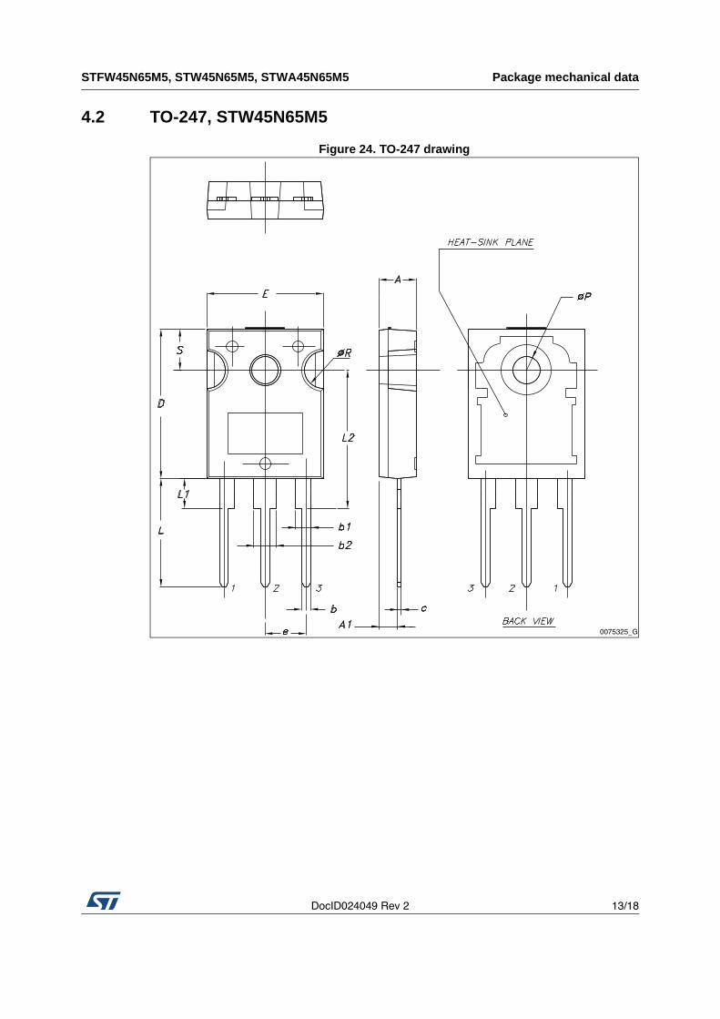
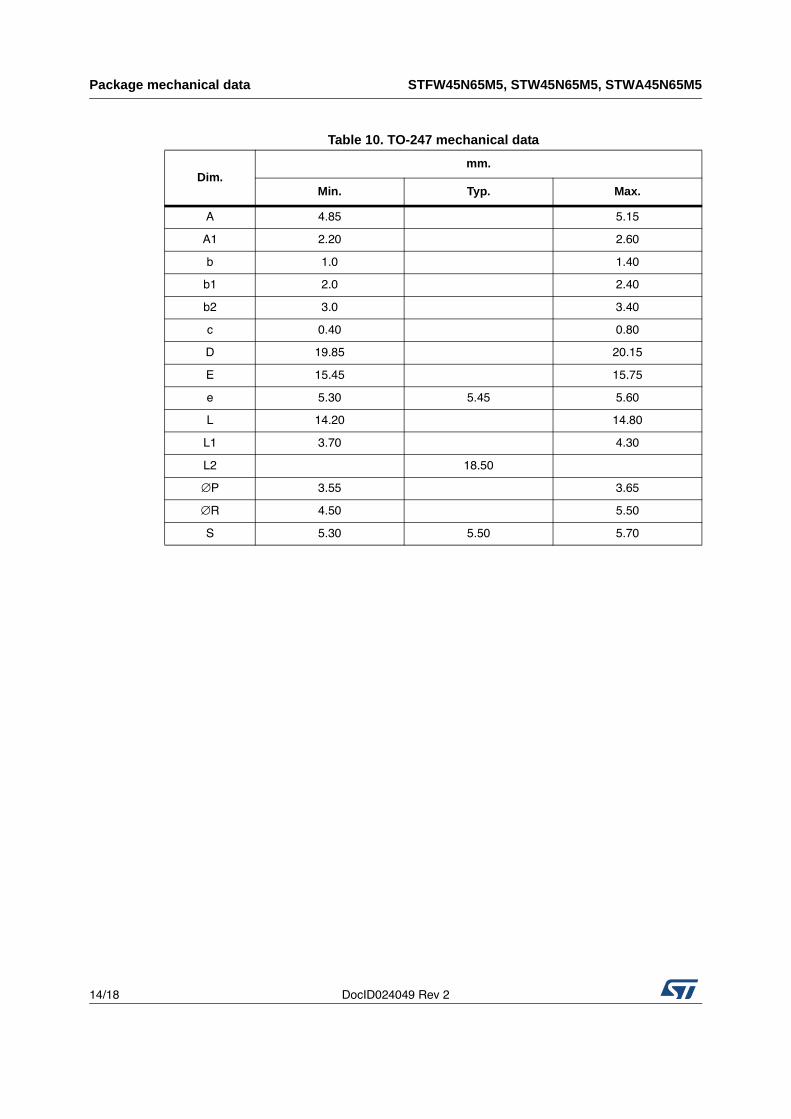
4.2 TO-247, STW45N65M5
Figure 24. TO-247 drawing
0075325_G
Package mechanical data STFW45N65M5, STW45N65M5, STWA45N65M5
14/18 DocID024049 Rev 2
Table 10. TO-247 mechanical data
Dim.mm.
Min. Typ. Max.
A 4.85 5.15
A1 2.20 2.60
b 1.0 1.40
b1 2.0 2.40
b2 3.0 3.40
c 0.40 0.80
D 19.85 20.15
E 15.45 15.75
e 5.30 5.45 5.60
L 14.20 14.80
L1 3.70 4.30
L2 18.50
∅P 3.55 3.65
∅R 4.50 5.50
S 5.30 5.50 5.70
DocID024049 Rev 2 15/18
STFW45N65M5, STW45N65M5, STWA45N65M5 Package mechanical data
18
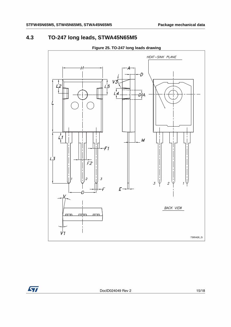
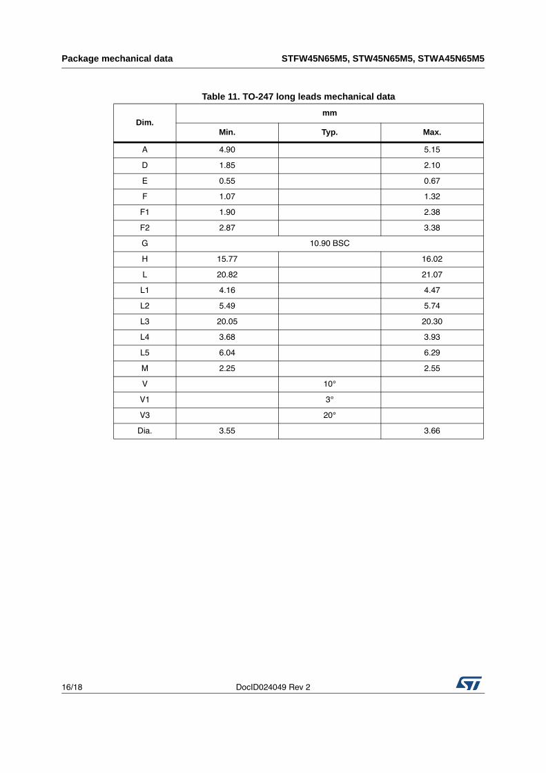
4.3 TO-247 long leads, STWA45N65M5
Figure 25. TO-247 long leads drawing
7395426_G
Package mechanical data STFW45N65M5, STW45N65M5, STWA45N65M5
16/18 DocID024049 Rev 2
Table 11. TO-247 long leads mechanical data
Dim.mm
Min. Typ. Max.
A 4.90 5.15
D 1.85 2.10
E 0.55 0.67
F 1.07 1.32
F1 1.90 2.38
F2 2.87 3.38
G 10.90 BSC
H 15.77 16.02
L 20.82 21.07
L1 4.16 4.47
L2 5.49 5.74
L3 20.05 20.30
L4 3.68 3.93
L5 6.04 6.29
M 2.25 2.55
V 10°
V1 3°
V3 20°
Dia. 3.55 3.66
DocID024049 Rev 2 17/18
STFW45N65M5, STW45N65M5, STWA45N65M5 Revision history
18
5 Revision history
2
Table 12. Document revision history
Date Revision Changes
11-Dec-2012 1 First release.
09-May-2014 2
– Added: TO-3PF package
– Added: dv/dt (MOSFET dv/dt ruggedness) parameter and VISO
– Modified: Figure 6 and 7
– Minor text changes
STFW45N65M5, STW45N65M5, STWA45N65M5
18/18 DocID024049 Rev 2
Please Read Carefully:
Information in this document is provided solely in connection with ST products. STMicroelectronics NV and its subsidiaries (“ST”) reserve the
right to make changes, corrections, modifications or improvements, to this document, and the products and services described herein at any
time, without notice.
All ST products are sold pursuant to ST’s terms and conditions of sale.
Purchasers are solely responsible for the choice, selection and use of the ST products and services described herein, and ST assumes no
liability whatsoever relating to the choice, selection or use of the ST products and services described herein.
No license, express or implied, by estoppel or otherwise, to any intellectual property rights is granted under this document. If any part of this
document refers to any third party products or services it shall not be deemed a license grant by ST for the use of such third party products
or services, or any intellectual property contained therein or considered as a warranty covering the use in any manner whatsoever of such
third party products or services or any intellectual property contained therein.
UNLESS OTHERWISE SET FORTH IN ST’S TERMS AND CONDITIONS OF SALE ST DISCLAIMS ANY EXPRESS OR IMPLIEDWARRANTY WITH RESPECT TO THE USE AND/OR SALE OF ST PRODUCTS INCLUDING WITHOUT LIMITATION IMPLIEDWARRANTIES OF MERCHANTABILITY, FITNESS FOR A PARTICULAR PURPOSE (AND THEIR EQUIVALENTS UNDER THE LAWSOF ANY JURISDICTION), OR INFRINGEMENT OF ANY PATENT, COPYRIGHT OR OTHER INTELLECTUAL PROPERTY RIGHT.
ST PRODUCTS ARE NOT DESIGNED OR AUTHORIZED FOR USE IN: (A) SAFETY CRITICAL APPLICATIONS SUCH AS LIFESUPPORTING, ACTIVE IMPLANTED DEVICES OR SYSTEMS WITH PRODUCT FUNCTIONAL SAFETY REQUIREMENTS; (B)AERONAUTIC APPLICATIONS; (C) AUTOMOTIVE APPLICATIONS OR ENVIRONMENTS, AND/OR (D) AEROSPACE APPLICATIONSOR ENVIRONMENTS. WHERE ST PRODUCTS ARE NOT DESIGNED FOR SUCH USE, THE PURCHASER SHALL USE PRODUCTS ATPURCHASER’S SOLE RISK, EVEN IF ST HAS BEEN INFORMED IN WRITING OF SUCH USAGE, UNLESS A PRODUCT ISEXPRESSLY DESIGNATED BY ST AS BEING INTENDED FOR “AUTOMOTIVE, AUTOMOTIVE SAFETY OR MEDICAL” INDUSTRYDOMAINS ACCORDING TO ST PRODUCT DESIGN SPECIFICATIONS. PRODUCTS FORMALLY ESCC, QML OR JAN QUALIFIED AREDEEMED SUITABLE FOR USE IN AEROSPACE BY THE CORRESPONDING GOVERNMENTAL AGENCY.
Resale of ST products with provisions different from the statements and/or technical features set forth in this document shall immediately void
any warranty granted by ST for the ST product or service described herein and shall not create or extend in any manner whatsoever, any
liability of ST.
ST and the ST logo are trademarks or registered trademarks of ST in various countries.
Information in this document supersedes and replaces all information previously supplied.
The ST logo is a registered trademark of STMicroelectronics. All other names are the property of their respective owners.
© 2014 STMicroelectronics - All rights reserved
STMicroelectronics group of companies
Australia - Belgium - Brazil - Canada - China - Czech Republic - Finland - France - Germany - Hong Kong - India - Israel - Italy - Japan -
Malaysia - Malta - Morocco - Philippines - Singapore - Spain - Sweden - Switzerland - United Kingdom - United States of America
www.st.com


![Multipacting in PIP-II 650 MHz.pptx [Read-Only]pxie.fnal.gov/PIPIImeetings/MultipactingInPIP-II_650MHz.pdf · Exponential growth rate 3 G.Romanov | Multipacting in PIP-II 650 MHz](https://static.fdocument.org/doc/165x107/5b8145247f8b9a466b8bfbbb/multipacting-in-pip-ii-650-mhzpptx-read-onlypxiefnalgovpipiimeetingsmultipactinginpip-ii.jpg)