N-channel 60V - 0.032 - 30A - TO-220 - D²PAK STripFET II Power … · June 2006 Rev 3 1/14 14...
14
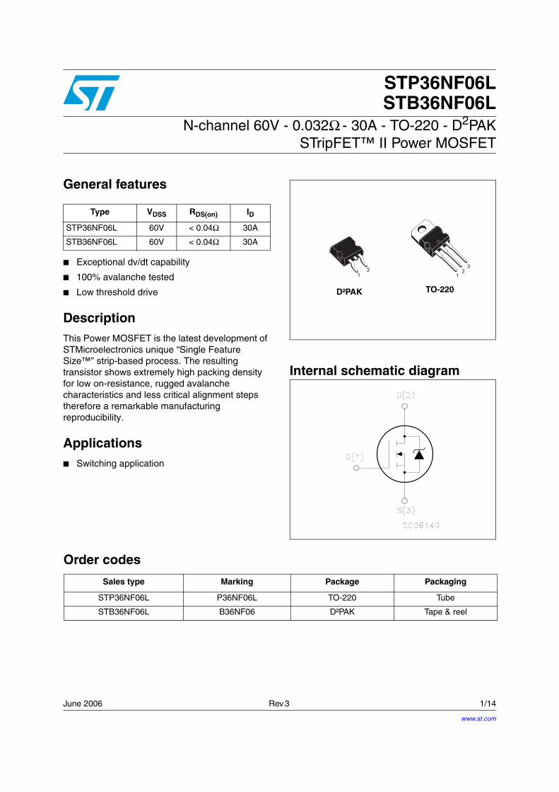
June 2006 Rev 3 1/14 14 STP36NF06L STB36NF06L N-channel 60V - 0.032Ω - 30A - TO-220 - D 2 PAK STripFET™ II Power MOSFET General features ■ Exceptional dv/dt capability ■ 100% avalanche tested ■ Low threshold drive Description This Power MOSFET is the latest development of STMicroelectronics unique “Single Feature Size™” strip-based process. The resulting transistor shows extremely high packing density for low on-resistance, rugged avalanche characteristics and less critical alignment steps therefore a remarkable manufacturing reproducibility. Applications ■ Switching application Internal schematic diagram Type V DSS R DS(on) I D STP36NF06L 60V < 0.04Ω 30A STB36NF06L 60V < 0.04Ω 30A D²PAK TO-220 1 2 3 1 3 www.st.com Order codes Sales type Marking Package Packaging STP36NF06L P36NF06L TO-220 Tube STB36NF06L B36NF06 D²PAK Tape & reel
Transcript of N-channel 60V - 0.032 - 30A - TO-220 - D²PAK STripFET II Power … · June 2006 Rev 3 1/14 14...
June 2006 Rev 3 1/14
14
STP36NF06LSTB36NF06L
N-channel 60V - 0.032Ω - 30A - TO-220 - D2PAKSTripFET™ II Power MOSFET
General features
Exceptional dv/dt capability
100% avalanche tested
Low threshold drive
DescriptionThis Power MOSFET is the latest development of STMicroelectronics unique “Single Feature Size™” strip-based process. The resulting transistor shows extremely high packing density for low on-resistance, rugged avalanche characteristics and less critical alignment steps therefore a remarkable manufacturing reproducibility.
Applications Switching application
Internal schematic diagram
Type VDSS RDS(on) ID
STP36NF06L 60V < 0.04Ω 30A
STB36NF06L 60V < 0.04Ω 30A
D²PAK TO-220
12
3
13
www.st.com
Order codes
Sales type Marking Package Packaging
STP36NF06L P36NF06L TO-220 Tube
STB36NF06L B36NF06 D²PAK Tape & reel
Contents: STP36NF06L - STB36NF06L
2/14
Contents:
1 Electrical ratings . . . . . . . . . . . . . . . . . . . . . . . . . . . . . . . . . . . . . . . . . . . . 3
2 Electrical characteristics . . . . . . . . . . . . . . . . . . . . . . . . . . . . . . . . . . . . . 4
2.1 Electrical characteristics (curves) . . . . . . . . . . . . . . . . . . . . . . . . . . . . . 6
3 Test circuit . . . . . . . . . . . . . . . . . . . . . . . . . . . . . . . . . . . . . . . . . . . . . . . . 8
4 Package mechanical data . . . . . . . . . . . . . . . . . . . . . . . . . . . . . . . . . . . . . 9
5 Packaging mechanical data . . . . . . . . . . . . . . . . . . . . . . . . . . . . . . . . . . 12
6 Revision history . . . . . . . . . . . . . . . . . . . . . . . . . . . . . . . . . . . . . . . . . . . 13
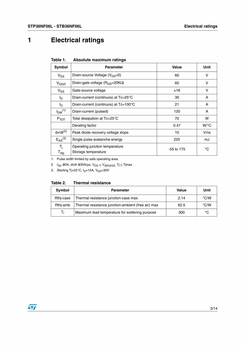
STP36NF06L - STB36NF06L Electrical ratings
3/14
1 Electrical ratings
Table 1. Absolute maximum ratings
Symbol Parameter Value Unit
VDS Drain-source Voltage (VGS=0) 60 V
VDGR Drain-gate voltage (RGS=20KΩ) 60 V
VGS Gate-source voltage ±18 V
ID Drain-current (continuos) at Tc=25°C 30 A
ID Drain-current (continuos) at Tc=100°C 21 A
IDM(1)
1. Pulse width limited by safe operating area.
Drain-current (pulsed) 120 A
PTOT Total dissipation at Tc=25°C 70 W
Derating factor 0.47 W/°C
dv/dt(2)
2. ISD ≤30A, di/dt ≤400A/µs, VDD < V(BR)DSS. Tj < Tjmax
Peak diode recovery voltage slope 10 V/ns
EAS(3)
3. Starting Tj=25°C, ID=15A, VDD=30V
Single pulse avalanche energy 225 mJ
Tj
Tstg
Operating junction temperature
Storage temperature-55 to 175 °C
Table 2. Thermal resistance
Symbol Parameter Value Unit
Rthj-case Thermal resistance junction-case max 2.14 °C/W
Rthj-amb Thermal resistance junction-ambient (free air) max 62.5 °C/W
Tl Maximum lead temperature for soldering purpose 300 °C
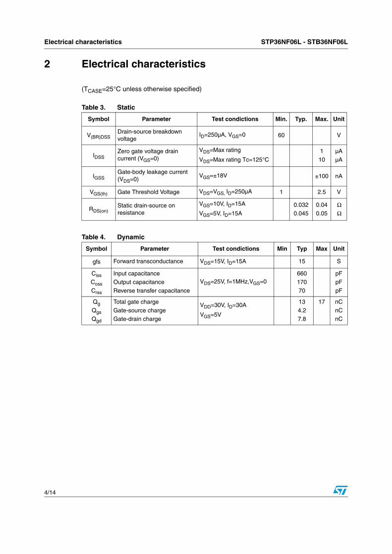
Electrical characteristics STP36NF06L - STB36NF06L
4/14
2 Electrical characteristics
(TCASE=25°C unless otherwise specified)
Table 3. Static
Symbol Parameter Test condictions Min. Typ. Max. Unit
V(BR)DSSDrain-source breakdown voltage
ID=250µA, VGS=0 60 V
IDSSZero gate voltage drain current (VGS=0)
VDS=Max rating
VDS=Max rating Tc=125°C
1
10
µA
µA
IGSSGate-body leakage current (VDS=0)
VGS=±18V ±100 nA
VGS(th) Gate Threshold Voltage VDS=VGS, ID=250µA 1 2.5 V
RDS(on)Static drain-source on resistance
VGS=10V, ID=15A
VGS=5V, ID=15A
0.032
0.045
0.04
0.05
ΩΩ
Table 4. Dynamic
Symbol Parameter Test condictions Min Typ Max Unit
gfs Forward transconductance VDS=15V, ID=15A 15 S
Ciss
Coss
Crss
Input capacitance
Output capacitance
Reverse transfer capacitance
VDS=25V, f=1MHz,VGS=0660
170
70
pF
pF
pF
Qg
Qgs
Qgd
Total gate charge
Gate-source chargeGate-drain charge
VDD=30V, ID=30A
VGS=5V
13
4.27.8
17 nC
nCnC
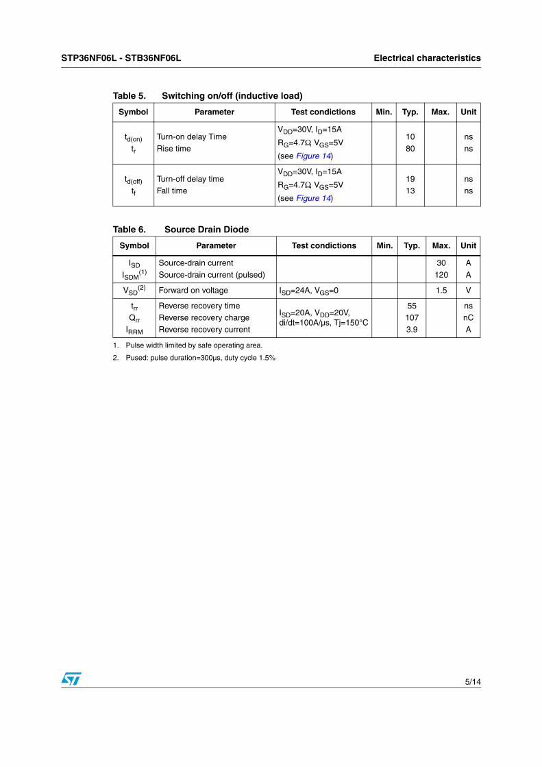
STP36NF06L - STB36NF06L Electrical characteristics
5/14
Table 5. Switching on/off (inductive load)
Symbol Parameter Test condictions Min. Typ. Max. Unit
td(on)
tr
Turn-on delay Time
Rise time
VDD=30V, ID=15A
RG=4.7Ω, VGS=5V
(see Figure 14)
10
80
ns
ns
td(off)
tf
Turn-off delay timeFall time
VDD=30V, ID=15A
RG=4.7Ω, VGS=5V
(see Figure 14)
1913
nsns
Table 6. Source Drain Diode
Symbol Parameter Test condictions Min. Typ. Max. Unit
ISD
ISDM(1)
1. Pulse width limited by safe operating area.
Source-drain current
Source-drain current (pulsed)
30
120
A
A
VSD(2)
2. Pused: pulse duration=300µs, duty cycle 1.5%
Forward on voltage ISD=24A, VGS=0 1.5 V
trrQrr
IRRM
Reverse recovery time
Reverse recovery chargeReverse recovery current
ISD=20A, VDD=20V, di/dt=100A/µs, Tj=150°C
55
1073.9
ns
nCA
Electrical characteristics STP36NF06L - STB36NF06L
6/14
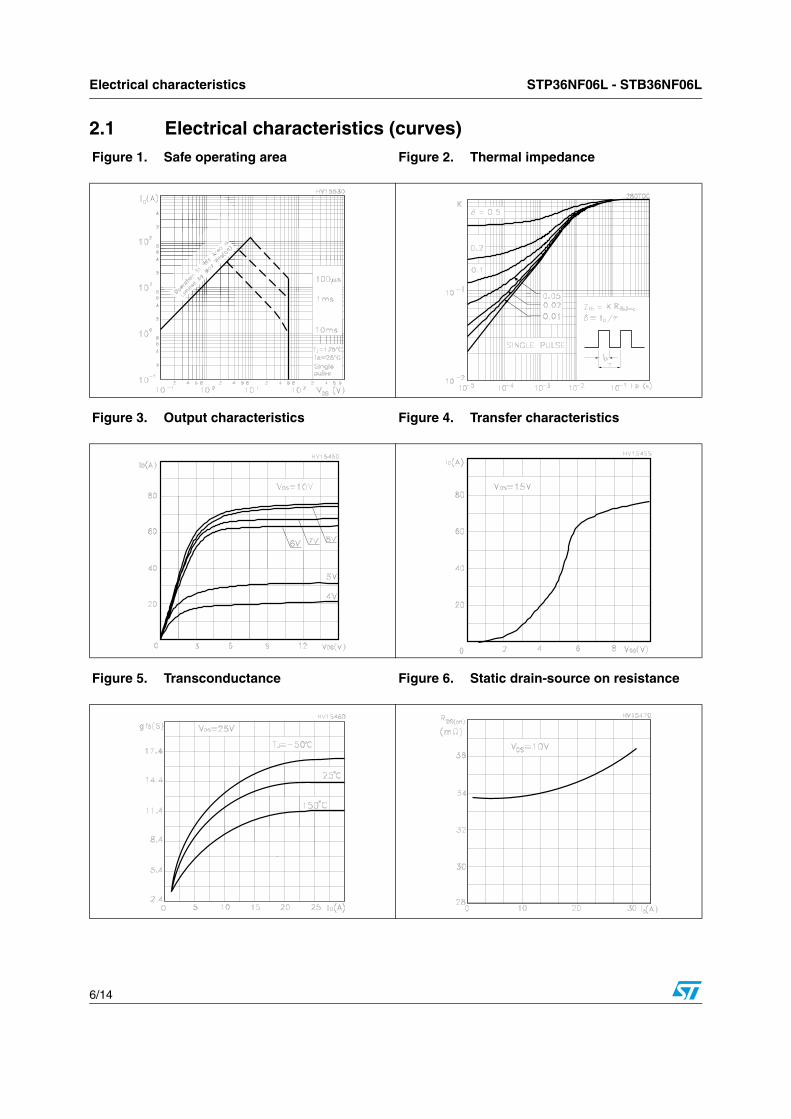
2.1 Electrical characteristics (curves) Figure 1. Safe operating area Figure 2. Thermal impedance
Figure 3. Output characteristics Figure 4. Transfer characteristics
Figure 5. Transconductance Figure 6. Static drain-source on resistance
STP36NF06L - STB36NF06L Electrical characteristics
7/14
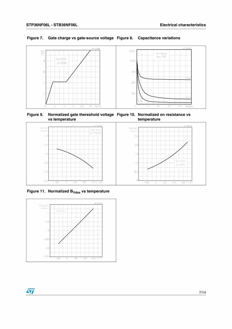
Figure 7. Gate charge vs gate-source voltage Figure 8. Capacitance variations
Figure 9. Normalized gate thereshold voltage vs temperature
Figure 10. Normalized on resistance vs temperature
Figure 11. Normalized BVdss vs temperature
Test circuit STP36NF06L - STB36NF06L
8/14
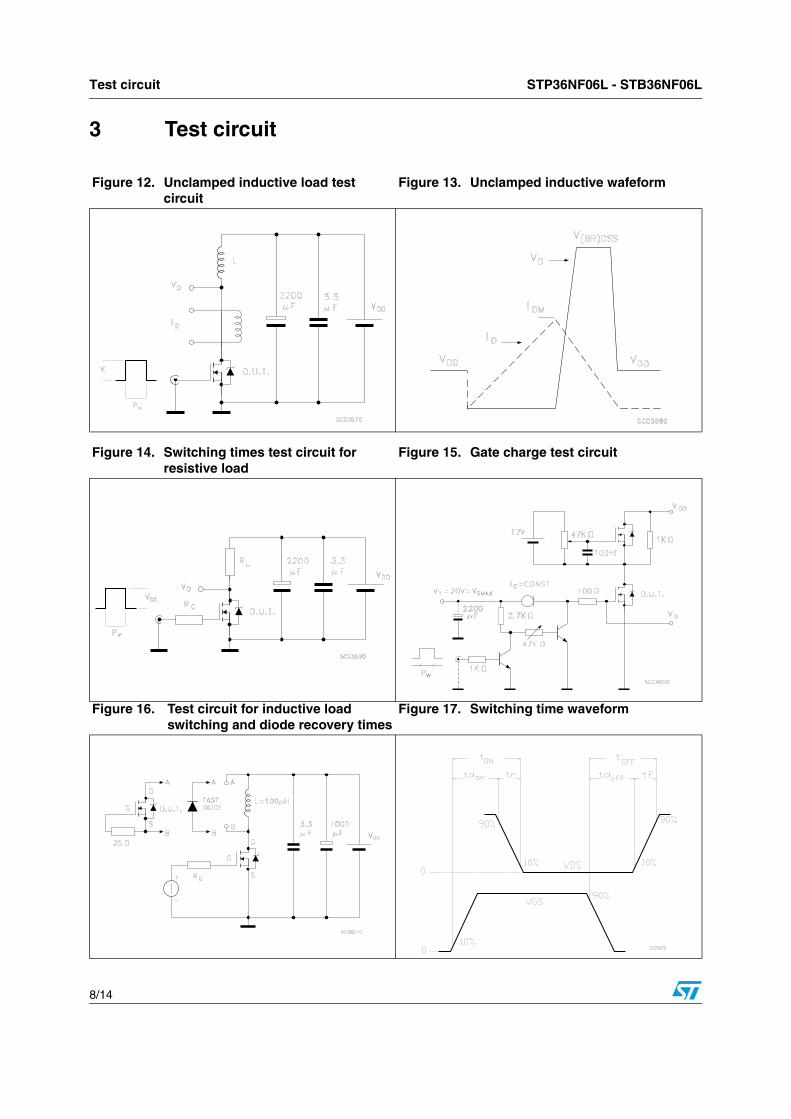
3 Test circuit
Figure 12. Unclamped inductive load test circuit
Figure 13. Unclamped inductive wafeform
Figure 14. Switching times test circuit for resistive load
Figure 15. Gate charge test circuit
Figure 16. Test circuit for inductive load switching and diode recovery times
Figure 17. Switching time waveform
STP36NF06L - STB36NF06L Package mechanical data
9/14
4 Package mechanical data
In order to meet environmental requirements, ST offers these devices in ECOPACK® packages. These packages have a Lead-free second level interconnect . The category of second level interconnect is marked on the package and on the inner box label, in compliance with JEDEC Standard JESD97. The maximum ratings related to soldering conditions are also marked on the inner box label. ECOPACK is an ST trademark. ECOPACK specifications are available at: www.st.com
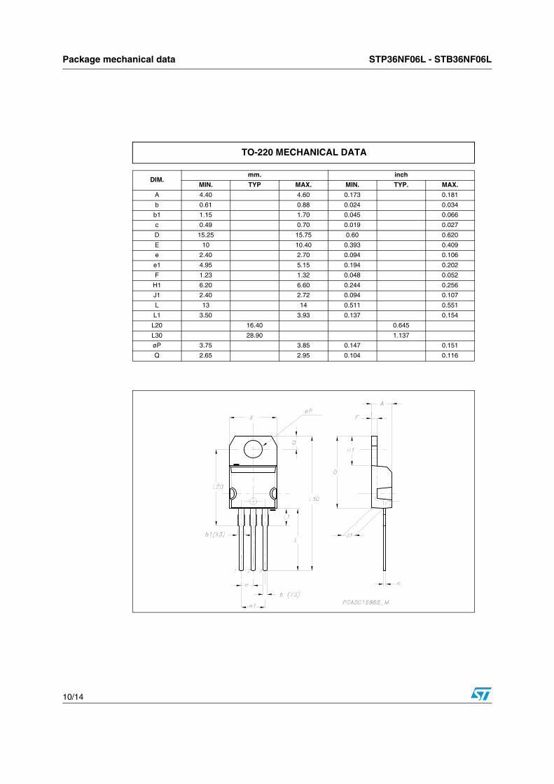
Package mechanical data STP36NF06L - STB36NF06L
10/14
DIM.mm. inch
MIN. TYP MAX. MIN. TYP. MAX.
A 4.40 4.60 0.173 0.181
b 0.61 0.88 0.024 0.034
b1 1.15 1.70 0.045 0.066
c 0.49 0.70 0.019 0.027
D 15.25 15.75 0.60 0.620
E 10 10.40 0.393 0.409
e 2.40 2.70 0.094 0.106
e1 4.95 5.15 0.194 0.202
F 1.23 1.32 0.048 0.052
H1 6.20 6.60 0.244 0.256
J1 2.40 2.72 0.094 0.107
L 13 14 0.511 0.551
L1 3.50 3.93 0.137 0.154
L20 16.40 0.645
L30 28.90 1.137
øP 3.75 3.85 0.147 0.151
Q 2.65 2.95 0.104 0.116
TO-220 MECHANICAL DATA
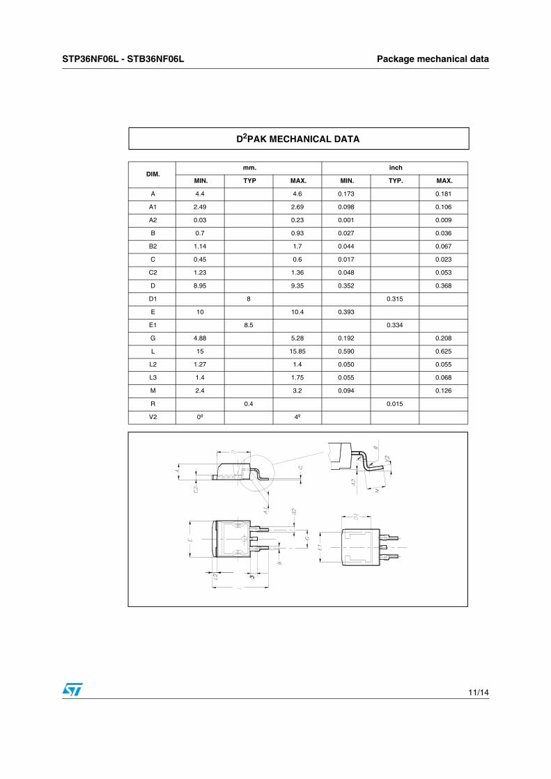
STP36NF06L - STB36NF06L Package mechanical data
11/14
TO-247 MECHANICAL DATA
1
DIM.mm. inch
MIN. TYP MAX. MIN. TYP. MAX.
A 4.4 4.6 0.173 0.181
A1 2.49 2.69 0.098 0.106
A2 0.03 0.23 0.001 0.009
B 0.7 0.93 0.027 0.036
B2 1.14 1.7 0.044 0.067
C 0.45 0.6 0.017 0.023
C2 1.23 1.36 0.048 0.053
D 8.95 9.35 0.352 0.368
D1 8 0.315
E 10 10.4 0.393
E1 8.5 0.334
G 4.88 5.28 0.192 0.208
L 15 15.85 0.590 0.625
L2 1.27 1.4 0.050 0.055
L3 1.4 1.75 0.055 0.068
M 2.4 3.2 0.094 0.126
R 0.4 0.015
V2 0º 4º
D2PAK MECHANICAL DATA
3
Packaging mechanical data STP36NF06L - STB36NF06L
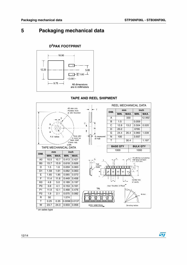
12/14
5 Packaging mechanical data
TAPE AND REEL SHIPMENT
D2PAK FOOTPRINT
* on sales type
DIM.mm inch
MIN. MAX. MIN. MAX.
A 330 12.992
B 1.5 0.059
C 12.8 13.2 0.504 0.520
D 20.2 0795
G 24.4 26.4 0.960 1.039
N 100 3.937
T 30.4 1.197
BASE QTY BULK QTY
1000 1000
REEL MECHANICAL DATA
DIM.mm inch
MIN. MAX. MIN. MAX.
A0 10.5 10.7 0.413 0.421
B0 15.7 15.9 0.618 0.626
D 1.5 1.6 0.059 0.063
D1 1.59 1.61 0.062 0.063
E 1.65 1.85 0.065 0.073
F 11.4 11.6 0.449 0.456
K0 4.8 5.0 0.189 0.197
P0 3.9 4.1 0.153 0.161
P1 11.9 12.1 0.468 0.476
P2 1.9 2.1 0.075 0.082
R 50 1.574
T 0.25 0.35 0.0098 0.0137
W 23.7 24.3 0.933 0.956
TAPE MECHANICAL DATA
STP36NF06L - STB36NF06L Revision history
13/14
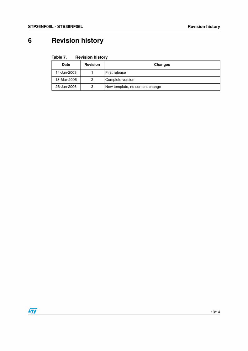
6 Revision history
Table 7. Revision history
Date Revision Changes
14-Jun-2003 1 First release
13-Mar-2006 2 Complete version
26-Jun-2006 3 New template, no content change
STP36NF06L - STB36NF06L
14/14
Please Read Carefully:
Information in this document is provided solely in connection with ST products. STMicroelectronics NV and its subsidiaries (“ST”) reserve theright to make changes, corrections, modifications or improvements, to this document, and the products and services described herein at anytime, without notice.
All ST products are sold pursuant to ST’s terms and conditions of sale.
Purchasers are solely responsible for the choice, selection and use of the ST products and services described herein, and ST assumes noliability whatsoever relating to the choice, selection or use of the ST products and services described herein.
No license, express or implied, by estoppel or otherwise, to any intellectual property rights is granted under this document. If any part of thisdocument refers to any third party products or services it shall not be deemed a license grant by ST for the use of such third party productsor services, or any intellectual property contained therein or considered as a warranty covering the use in any manner whatsoever of suchthird party products or services or any intellectual property contained therein.
UNLESS OTHERWISE SET FORTH IN ST’S TERMS AND CONDITIONS OF SALE ST DISCLAIMS ANY EXPRESS OR IMPLIEDWARRANTY WITH RESPECT TO THE USE AND/OR SALE OF ST PRODUCTS INCLUDING WITHOUT LIMITATION IMPLIEDWARRANTIES OF MERCHANTABILITY, FITNESS FOR A PARTICULAR PURPOSE (AND THEIR EQUIVALENTS UNDER THE LAWSOF ANY JURISDICTION), OR INFRINGEMENT OF ANY PATENT, COPYRIGHT OR OTHER INTELLECTUAL PROPERTY RIGHT.
UNLESS EXPRESSLY APPROVED IN WRITING BY AN AUTHORIZE REPRESENTATIVE OF ST, ST PRODUCTS ARE NOT DESIGNED,AUTHORIZED OR WARRANTED FOR USE IN MILITARY, AIR CRAFT, SPACE, LIFE SAVING, OR LIFE SUSTAINING APPLICATIONS,NOR IN PRODUCTS OR SYSTEMS, WHERE FAILURE OR MALFUNCTION MAY RESULT IN PERSONAL INJURY, DEATH, ORSEVERE PROPERTY OR ENVIRONMENTAL DAMAGE.
Resale of ST products with provisions different from the statements and/or technical features set forth in this document shall immediately voidany warranty granted by ST for the ST product or service described herein and shall not create or extend in any manner whatsoever, anyliability of ST.
ST and the ST logo are trademarks or registered trademarks of ST in various countries.
Information in this document supersedes and replaces all information previously supplied.
The ST logo is a registered trademark of STMicroelectronics. All other names are the property of their respective owners.
© 2006 STMicroelectronics - All rights reserved
STMicroelectronics group of companies
Australia - Belgium - Brazil - Canada - China - Czech Republic - Finland - France - Germany - Hong Kong - India - Israel - Italy - Japan - Malaysia - Malta - Morocco - Singapore - Spain - Sweden - Switzerland - United Kingdom - United States of America
www.st.com