N-CHANNEL 600V - Farnell element14 · N-CHANNEL 600V - 8Ω - 1A DPAK/TO-92/IPAK/SOT-223...
15
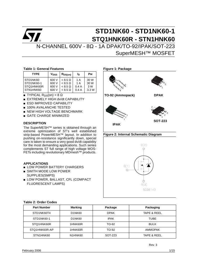
1/15 February 2006 STD1NK60 - STD1NK60-1 STQ1HNK60R - STN1HNK60 N-CHANNEL 600V - 8Ω - 1A DPAK/TO-92/IPAK/SOT-223 SuperMESH™ MOSFET Table 1: General Features ■ TYPICAL R DS (on) = 8 Ω ■ EXTREMELY HIGH dv/dt CAPABILITY ■ ESD IMPROVED CAPABILITY ■ 100% AVALANCHE TESTED ■ NEW HIGH VOLTAGE BENCHMARK ■ GATE CHARGE MINIMIZED DESCRIPTION The SuperMESH™ series is obtained through an extreme optimization of ST’s well established strip-based PowerMESH™ layout. In addition to pushing on-resistance significantly down, special care is taken to ensure a very good dv/dt capability for the most demanding applications. Such series complements ST full range of high voltage MOS- FETs including revolutionary MDmesh™ products. APPLICATIONS ■ LOW POWER BATTERY CHARGERS ■ SWITH MODE LOW POWER SUPPLIES(SMPS) ■ LOW POWER, BALLAST, CFL (COMPACT FLUORESCENT LAMPS) Table 2: Order Codes Figure 1: Package Figure 2: Internal Schematic Diagram TYPE V DSS R DS(on) I D Pw STD1NK60 STD1NK60-1 STQ1HNK60R STN1HNK60 600 V 600 V 600 V 600 V < 8.5 Ω < 8.5 Ω < 8.5 Ω < 8.5 Ω 1 A 1 A 0.4 A 0.4 A 30 W 30 W 3 W 3.3 W 3 2 1 TO-92 (Ammopack) IPAK 1 2 2 3 SOT-223 1 3 DPAK Part Number Marking Package Packaging STD1NK60T4 D1NK60 DPAK TAPE & REEL STD1NK60-1 D1NK60 IPAK TUBE STQ1HNK60R 1HNK60R TO-92 BULK STQ1HNK60R-AP 1HNK60R TO-92 AMMOPAK STN1HNK60 N1HNK60 SOT-223 TAPE & REEL Rev. 3
Transcript of N-CHANNEL 600V - Farnell element14 · N-CHANNEL 600V - 8Ω - 1A DPAK/TO-92/IPAK/SOT-223...
1/15February 2006
STD1NK60 - STD1NK60-1STQ1HNK60R - STN1HNK60
N-CHANNEL 600V - 8Ω - 1A DPAK/TO-92/IPAK/SOT-223SuperMESH™ MOSFET
Table 1: General Features
TYPICAL RDS(on) = 8 Ω EXTREMELY HIGH dv/dt CAPABILITY ESD IMPROVED CAPABILITY 100% AVALANCHE TESTED NEW HIGH VOLTAGE BENCHMARK GATE CHARGE MINIMIZED
DESCRIPTIONThe SuperMESH™ series is obtained through anextreme optimization of ST’s well establishedstrip-based PowerMESH™ layout. In addition topushing on-resistance significantly down, specialcare is taken to ensure a very good dv/dt capabilityfor the most demanding applications. Such seriescomplements ST full range of high voltage MOS-FETs including revolutionary MDmesh™ products.
APPLICATIONS LOW POWER BATTERY CHARGERS SWITH MODE LOW POWER
SUPPLIES(SMPS) LOW POWER, BALLAST, CFL (COMPACT
FLUORESCENT LAMPS)
Table 2: Order Codes
Figure 1: Package
Figure 2: Internal Schematic Diagram
TYPE VDSS RDS(on) ID Pw
STD1NK60STD1NK60-1STQ1HNK60RSTN1HNK60
600 V600 V600 V600 V
< 8.5 Ω< 8.5 Ω< 8.5 Ω< 8.5 Ω
1 A1 A
0.4 A 0.4 A
30 W30 W3 W
3.3 W
32
1
TO-92 (Ammopack)
IPAK
12
2
3
SOT-223
1
3
DPAK
Part Number Marking Package Packaging
STD1NK60T4 D1NK60 DPAK TAPE & REEL
STD1NK60-1 D1NK60 IPAK TUBE
STQ1HNK60R 1HNK60R TO-92 BULK
STQ1HNK60R-AP 1HNK60R TO-92 AMMOPAK
STN1HNK60 N1HNK60 SOT-223 TAPE & REEL
Rev. 3
STD1NK60 - STD1NK60-1 - STQ1HNK60R - STN1HNK60
2/15
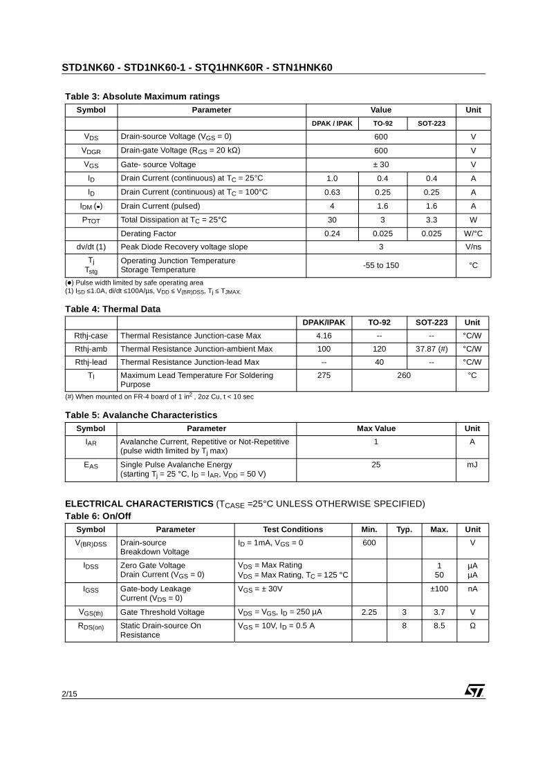
Table 3: Absolute Maximum ratings
() Pulse width limited by safe operating area (1) ISD ≤1.0A, di/dt ≤100A/µs, VDD ≤ V(BR)DSS, Tj ≤ TJMAX.
Table 4: Thermal Data
(#) When mounted on FR-4 board of 1 in2 , 2oz Cu, t < 10 sec
Table 5: Avalanche Characteristics
ELECTRICAL CHARACTERISTICS (TCASE =25°C UNLESS OTHERWISE SPECIFIED)Table 6: On/Off
Symbol Parameter Value Unit
DPAK / IPAK TO-92 SOT-223
VDS Drain-source Voltage (VGS = 0) 600 V
VDGR Drain-gate Voltage (RGS = 20 kΩ) 600 V
VGS Gate- source Voltage ± 30 V
ID Drain Current (continuous) at TC = 25°C 1.0 0.4 0.4 A
ID Drain Current (continuous) at TC = 100°C 0.63 0.25 0.25 A
IDM () Drain Current (pulsed) 4 1.6 1.6 A
PTOT Total Dissipation at TC = 25°C 30 3 3.3 W
Derating Factor 0.24 0.025 0.025 W/°C
dv/dt (1) Peak Diode Recovery voltage slope 3 V/ns
TjTstg
Operating Junction TemperatureStorage Temperature -55 to 150 °C
DPAK/IPAK TO-92 SOT-223 Unit
Rthj-case Thermal Resistance Junction-case Max 4.16 -- -- °C/W
Rthj-amb Thermal Resistance Junction-ambient Max 100 120 37.87 (#) °C/W
Rthj-lead Thermal Resistance Junction-lead Max -- 40 -- °C/W
Tl Maximum Lead Temperature For Soldering Purpose
275 260 °C
Symbol Parameter Max Value Unit
IAR Avalanche Current, Repetitive or Not-Repetitive(pulse width limited by Tj max)
1 A
EAS Single Pulse Avalanche Energy(starting Tj = 25 °C, ID = IAR, VDD = 50 V)
25 mJ
Symbol Parameter Test Conditions Min. Typ. Max. Unit
V(BR)DSS Drain-source Breakdown Voltage
ID = 1mA, VGS = 0 600 V
IDSS Zero Gate Voltage Drain Current (VGS = 0)
VDS = Max RatingVDS = Max Rating, TC = 125 °C
150
µAµA
IGSS Gate-body LeakageCurrent (VDS = 0)
VGS = ± 30V ±100 nA
VGS(th) Gate Threshold Voltage VDS = VGS, ID = 250 µA 2.25 3 3.7 V
RDS(on) Static Drain-source On Resistance
VGS = 10V, ID = 0.5 A 8 8.5 Ω
3/15
STD1NK60 - STD1NK60-1 - STQ1HNK60R - STN1HNK60
ELECTRICAL CHARACTERISTICS (CONTINUED)
Table 7: Dynamic
Table 8: Source Drain Diode
(1) Pulsed: Pulse duration = 300 µs, duty cycle 1.5 %.(2) Pulse width limited by safe operating area.
Symbol Parameter Test Conditions Min. Typ. Max. Unit
gfs (1) Forward Transconductance VDS = 15 V, ID= 0.5 A 1 S
CissCossCrss
Input CapacitanceOutput CapacitanceReverse Transfer Capacitance
VDS = 25V, f = 1 MHz, VGS = 0 15623.53.8
pFpFpF
td(on)tr
td(off)tr
Turn-on Delay Time Rise TimeTurn-off Delay TimeFall Time
VDD = 300 V, ID = 0.5 A,RG= 4.7 Ω, VGS = 10 V(Resistive Load see, Figure 21)
6.551925
nsnsnsns
QgQgsQgd
Total Gate ChargeGate-Source ChargeGate-Drain Charge
VDD = 480V, ID = 1 A,VGS = 10V, RG= 4.7 Ω(see, Figure 23)
71.13.7
10 nCnCnC
Symbol Parameter Test Conditions Min. Typ. Max. Unit
ISDISDM (2)
Source-drain CurrentSource-drain Current (pulsed)
14
AA
VSD (1) Forward On Voltage ISD = 1.0 A, VGS = 0 1.6 V
trrQrr
IRRM
Reverse Recovery TimeReverse Recovery ChargeReverse Recovery Current
ISD = 1.0 A, di/dt = 100 A/µsVDD = 25V, Tj = 25°C(see test circuit, Figure 22)
1402403.3
nsµCA
trrQrr
IRRM
Reverse Recovery TimeReverse Recovery ChargeReverse Recovery Current
ISD = 1.0 A, di/dt = 100 A/µsVDD = 25V, Tj = 150°C(see test circuit, Figure 22)
2293773.3
nsµCA
STD1NK60 - STD1NK60-1 - STQ1HNK60R - STN1HNK60
4/15
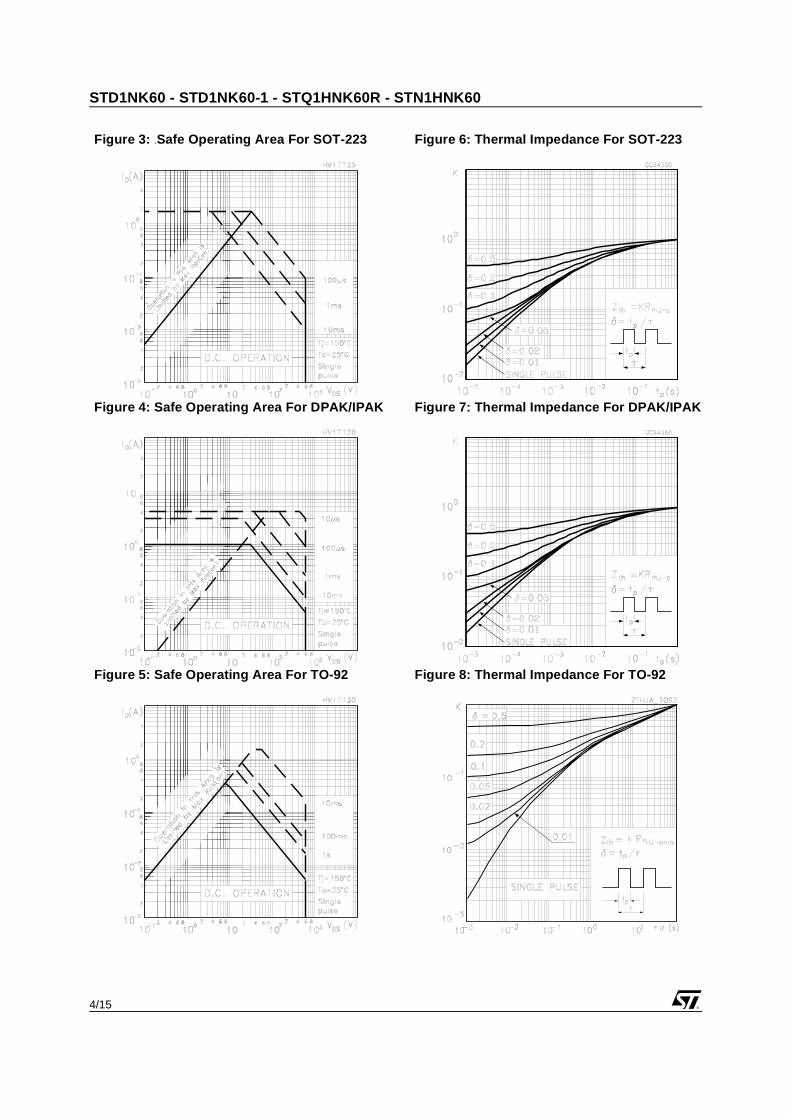
Figure 3: .Safe Operating Area For SOT-223
Figure 4: Safe Operating Area For DPAK/IPAK
Figure 5: Safe Operating Area For TO-92
Figure 6: Thermal Impedance For SOT-223
Figure 7: Thermal Impedance For DPAK/IPAK
Figure 8: Thermal Impedance For TO-92
5/15
STD1NK60 - STD1NK60-1 - STQ1HNK60R - STN1HNK60
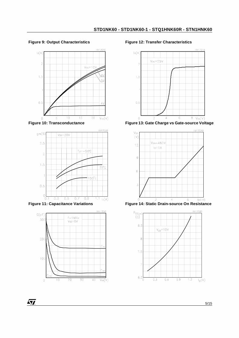
Figure 9: Output Characteristics
Figure 10: Transconductance
Figure 11: Capacitance Variations
Figure 12: Transfer Characteristics
Figure 13: Gate Charge vs Gate-source Voltage
Figure 14: Static Drain-source On Resistance
STD1NK60 - STD1NK60-1 - STQ1HNK60R - STN1HNK60
6/15
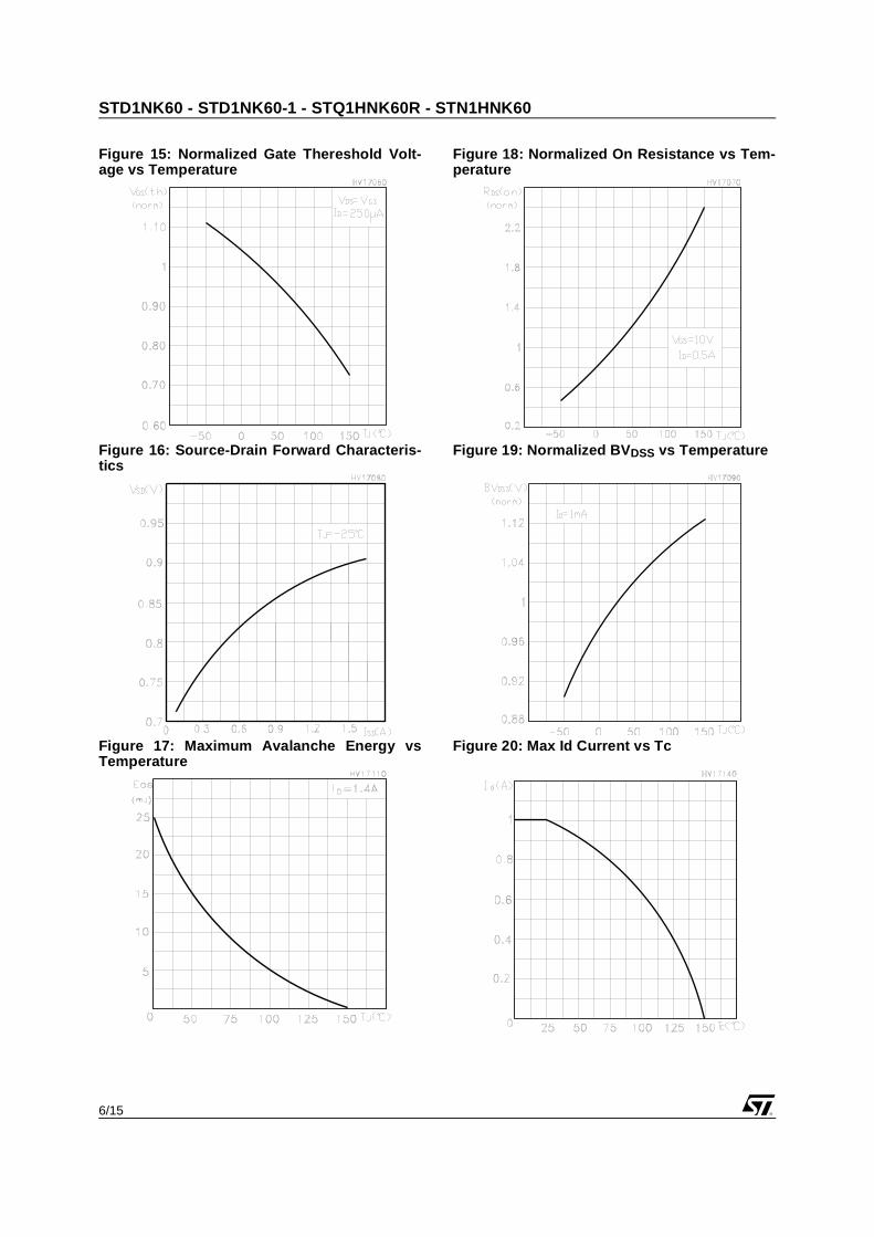
Figure 15: Normalized Gate Thereshold Volt-age vs Temperature
Figure 16: Source-Drain Forward Characteris-tics
Figure 17: Maximum Avalanche Energy vsTemperature
Figure 18: Normalized On Resistance vs Tem-perature
Figure 19: Normalized BVDSS vs Temperature
Figure 20: Max Id Current vs Tc
7/15
STD1NK60 - STD1NK60-1 - STQ1HNK60R - STN1HNK60
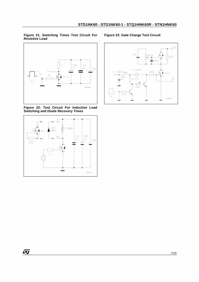
Figure 21: Switching Times Test Circuit ForResistive Load
Figure 22: Test Circuit For Inductive LoadSwitching and Diode Recovery Times
Figure 23: Gate Charge Test Circuit
STD1NK60 - STD1NK60-1 - STQ1HNK60R - STN1HNK60
8/15
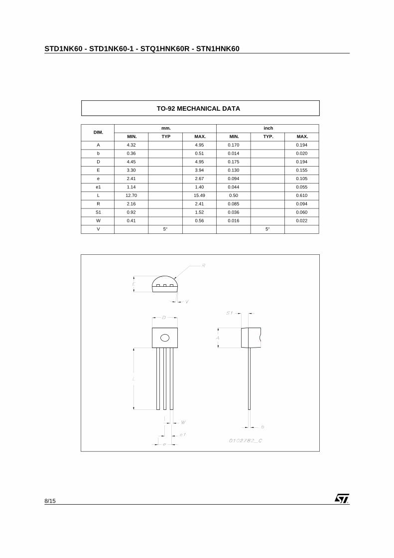
DIM.mm. inch
MIN. TYP MAX. MIN. TYP. MAX.
A 4.32 4.95 0.170 0.194
b 0.36 0.51 0.014 0.020
D 4.45 4.95 0.175 0.194
E 3.30 3.94 0.130 0.155
e 2.41 2.67 0.094 0.105
e1 1.14 1.40 0.044 0.055
L 12.70 15.49 0.50 0.610
R 2.16 2.41 0.085 0.094
S1 0.92 1.52 0.036 0.060
W 0.41 0.56 0.016 0.022
V 5° 5°
TO-92 MECHANICAL DATA
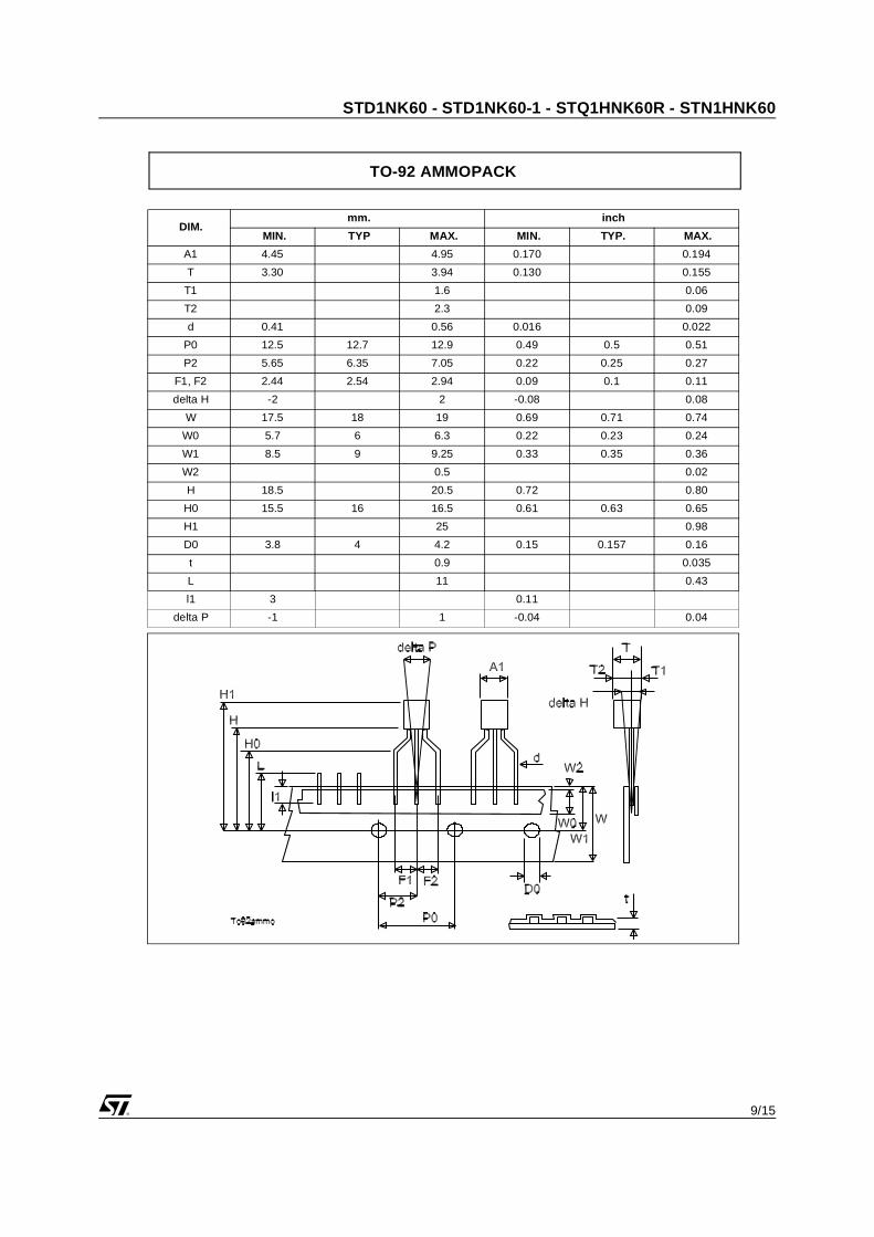
9/15
STD1NK60 - STD1NK60-1 - STQ1HNK60R - STN1HNK60
DIM.mm. inch
MIN. TYP MAX. MIN. TYP. MAX.
A1 4.45 4.95 0.170 0.194
T 3.30 3.94 0.130 0.155
T1 1.6 0.06
T2 2.3 0.09
d 0.41 0.56 0.016 0.022
P0 12.5 12.7 12.9 0.49 0.5 0.51
P2 5.65 6.35 7.05 0.22 0.25 0.27
F1, F2 2.44 2.54 2.94 0.09 0.1 0.11
delta H -2 2 -0.08 0.08
W 17.5 18 19 0.69 0.71 0.74
W0 5.7 6 6.3 0.22 0.23 0.24
W1 8.5 9 9.25 0.33 0.35 0.36
W2 0.5 0.02
H 18.5 20.5 0.72 0.80
H0 15.5 16 16.5 0.61 0.63 0.65
H1 25 0.98
D0 3.8 4 4.2 0.15 0.157 0.16
t 0.9 0.035
L 11 0.43
l1 3 0.11
delta P -1 1 -0.04 0.04
TO-92 AMMOPACK
STD1NK60 - STD1NK60-1 - STQ1HNK60R - STN1HNK60
10/15
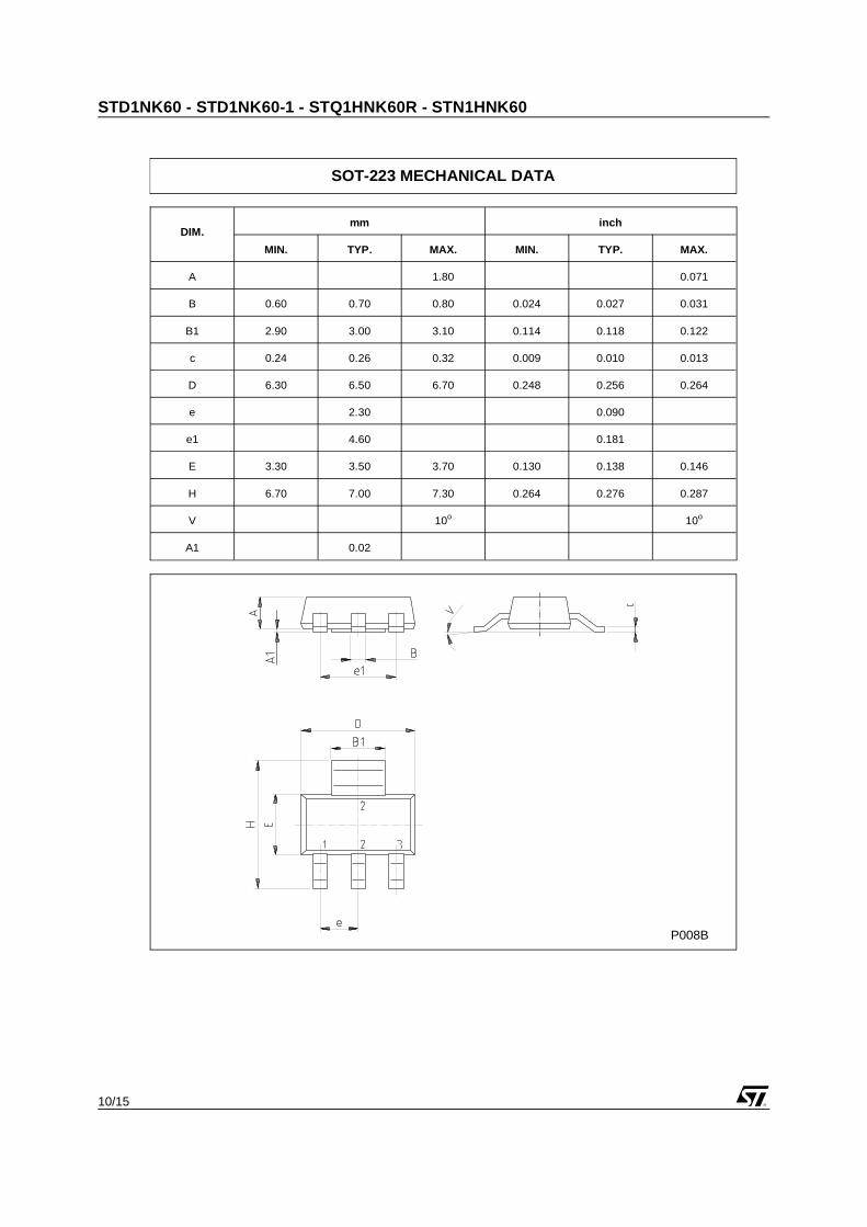
DIM.mm inch
MIN. TYP. MAX. MIN. TYP. MAX.
A 1.80 0.071
B 0.60 0.70 0.80 0.024 0.027 0.031
B1 2.90 3.00 3.10 0.114 0.118 0.122
c 0.24 0.26 0.32 0.009 0.010 0.013
D 6.30 6.50 6.70 0.248 0.256 0.264
e 2.30 0.090
e1 4.60 0.181
E 3.30 3.50 3.70 0.130 0.138 0.146
H 6.70 7.00 7.30 0.264 0.276 0.287
V 10o 10o
A1 0.02
P008B
SOT-223 MECHANICAL DATA
11/15
STD1NK60 - STD1NK60-1 - STQ1HNK60R - STN1HNK60
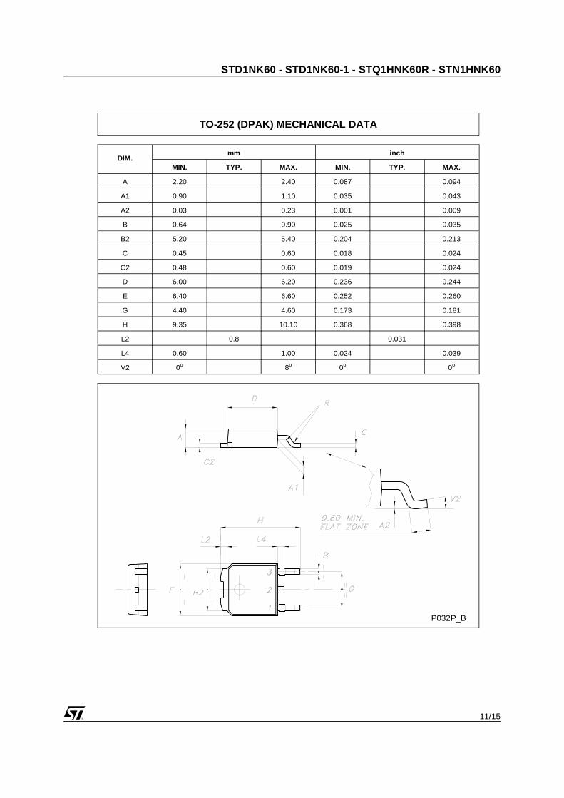
DIM.mm inch
MIN. TYP. MAX. MIN. TYP. MAX.
A 2.20 2.40 0.087 0.094
A1 0.90 1.10 0.035 0.043
A2 0.03 0.23 0.001 0.009
B 0.64 0.90 0.025 0.035
B2 5.20 5.40 0.204 0.213
C 0.45 0.60 0.018 0.024
C2 0.48 0.60 0.019 0.024
D 6.00 6.20 0.236 0.244
E 6.40 6.60 0.252 0.260
G 4.40 4.60 0.173 0.181
H 9.35 10.10 0.368 0.398
L2 0.8 0.031
L4 0.60 1.00 0.024 0.039
V2 0o 8o 0o 0o
P032P_B
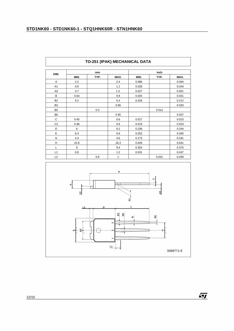
TO-252 (DPAK) MECHANICAL DATA
STD1NK60 - STD1NK60-1 - STQ1HNK60R - STN1HNK60
12/15
DIM.mm inch
MIN. TYP. MAX. MIN. TYP. MAX.
A 2.2 2.4 0.086 0.094
A1 0.9 1.1 0.035 0.043
A3 0.7 1.3 0.027 0.051
B 0.64 0.9 0.025 0.031
B2 5.2 5.4 0.204 0.212
B3 0.85 0.033
B5 0.3 0.012
B6 0.95 0.037
C 0.45 0.6 0.017 0.023
C2 0.48 0.6 0.019 0.023
D 6 6.2 0.236 0.244
E 6.4 6.6 0.252 0.260
G 4.4 4.6 0.173 0.181
H 15.9 16.3 0.626 0.641
L 9 9.4 0.354 0.370
L1 0.8 1.2 0.031 0.047
L2 0.8 1 0.031 0.039
A
C2
C
A3
H
A1
D LL2
L1
1 3
=
=
B3
B B
6
B2 E
G
=
=
=
=
B5
2
TO-251 (IPAK) MECHANICAL DATA
0068771-E
13/15
STD1NK60 - STD1NK60-1 - STQ1HNK60R - STN1HNK60
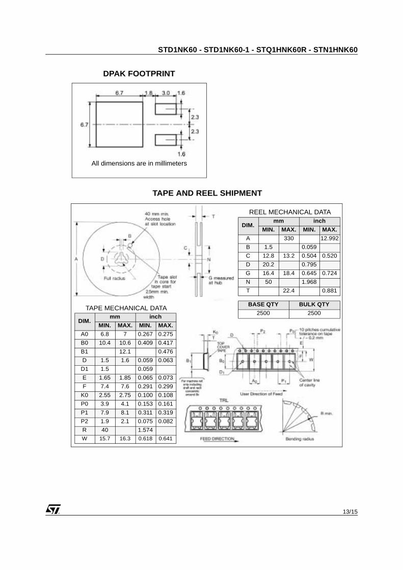
TAPE AND REEL SHIPMENT
DPAK FOOTPRINT
DIM.mm inch
MIN. MAX. MIN. MAX.
A 330 12.992
B 1.5 0.059
C 12.8 13.2 0.504 0.520
D 20.2 0.795
G 16.4 18.4 0.645 0.724
N 50 1.968
T 22.4 0.881
BASE QTY BULK QTY
2500 2500
REEL MECHANICAL DATA
DIM.mm inch
MIN. MAX. MIN. MAX.
A0 6.8 7 0.267 0.275
B0 10.4 10.6 0.409 0.417
B1 12.1 0.476
D 1.5 1.6 0.059 0.063
D1 1.5 0.059
E 1.65 1.85 0.065 0.073
F 7.4 7.6 0.291 0.299
K0 2.55 2.75 0.100 0.108
P0 3.9 4.1 0.153 0.161
P1 7.9 8.1 0.311 0.319
P2 1.9 2.1 0.075 0.082
R 40 1.574
W 15.7 16.3 0.618 0.641
TAPE MECHANICAL DATA
All dimensions are in millimeters
STD1NK60 - STD1NK60-1 - STQ1HNK60R - STN1HNK60
14/15
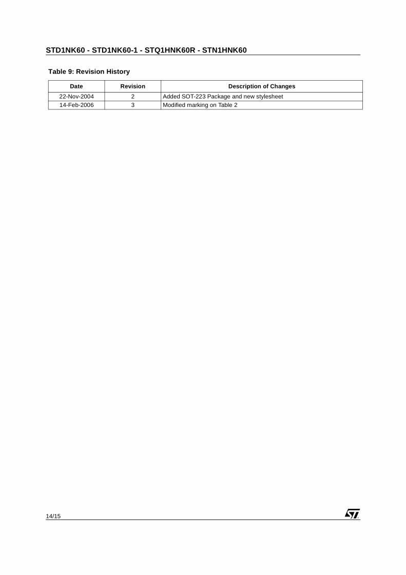
Table 9: Revision History
Date Revision Description of Changes
22-Nov-2004 2 Added SOT-223 Package and new stylesheet14-Feb-2006 3 Modified marking on Table 2
15/15
STD1NK60 - STD1NK60-1 - STQ1HNK60R - STN1HNK60
Information furnished is believed to be accurate and reliable. However, STMicroelectronics assumes no responsibility for the consequencesof use of such information nor for any infringement of patents or other rights of third parties which may result from its use. No license is grantedby implication or otherwise under any patent or patent rights of STMicroelectronics. Specifications mentioned in this publication are subjectto change without notice. This publication supersedes and replaces all information previously supplied. STMicroelectronics products are notauthorized for use as critical components in life support devices or systems without express written approval of STMicroelectronics.
The ST logo is a registered trademark of STMicroelectronics
All other names are the property of their respective owners
© 2006 STMicroelectronics - All Rights Reserved
STMicroelectronics group of companies
Australia - Belgium - Brazil - Canada - China - Czech Republic - Finland - France - Germany - Hong Kong - India - Israel - Italy - Japan - Malaysia - Malta - Morocco - Singapore - Spain - Sweden - Switzerland - United Kingdom - United States of America
www.st.com


![FQP12N60C / FQPF12N60C 600V N-Channel · PDF fileFQP12N60C / FQPF12N60C 600V N-Channel MOSFET September 2007 QFET ... Case Temperature [ ]](https://static.fdocument.org/doc/165x107/5aa9c8207f8b9a77188d4f43/fqp12n60c-fqpf12n60c-600v-n-channel-fqpf12n60c-600v-n-channel-mosfet-september.jpg)