
N-channel 600 V, 0.13 typ., 21 A MDmesh™ DM2 Power … Sheets/ST Microelectronics...
20
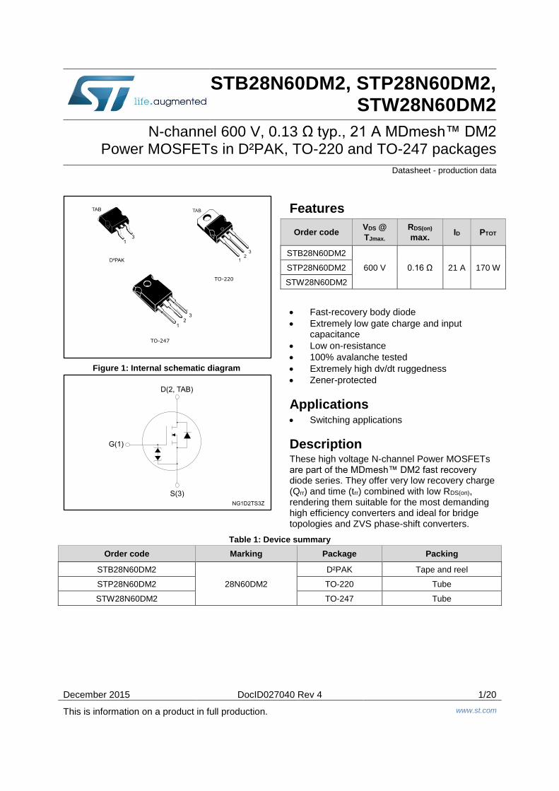
December 2015 DocID027040 Rev 4 1/20 This is information on a product in full production. www.st.com STB28N60DM2, STP28N60DM2, STW28N60DM2 N-channel 600 V, 0.13 Ω typ., 21 A MDmesh™ DM2 Power MOSFETs in D²PAK, TO-220 and TO-247 packages Datasheet - production data Figure 1: Internal schematic diagram Features Order code VDS @ TJmax. RDS(on) max. ID PTOT STB28N60DM2 600 V 0.16 Ω 21 A 170 W STP28N60DM2 STW28N60DM2 Fast-recovery body diode Extremely low gate charge and input capacitance Low on-resistance 100% avalanche tested Extremely high dv/dt ruggedness Zener-protected Applications Switching applications Description These high voltage N-channel Power MOSFETs are part of the MDmesh™ DM2 fast recovery diode series. They offer very low recovery charge (Qrr) and time (trr) combined with low RDS(on), rendering them suitable for the most demanding high efficiency converters and ideal for bridge topologies and ZVS phase-shift converters. Table 1: Device summary Order code Marking Package Packing STB28N60DM2 28N60DM2 D²PAK Tape and reel STP28N60DM2 TO-220 Tube STW28N60DM2 TO-247 Tube
Transcript of N-channel 600 V, 0.13 typ., 21 A MDmesh™ DM2 Power … Sheets/ST Microelectronics...
December 2015 DocID027040 Rev 4 1/20
This is information on a product in full production. www.st.com
STB28N60DM2, STP28N60DM2, STW28N60DM2
N-channel 600 V, 0.13 Ω typ., 21 A MDmesh™ DM2 Power MOSFETs in D²PAK, TO-220 and TO-247 packages
Datasheet - production data
Figure 1: Internal schematic diagram
Features
Order code VDS @
TJmax.
RDS(on)
max. ID PTOT
STB28N60DM2
600 V 0.16 Ω 21 A 170 W STP28N60DM2
STW28N60DM2
Fast-recovery body diode
Extremely low gate charge and input capacitance
Low on-resistance
100% avalanche tested
Extremely high dv/dt ruggedness
Zener-protected
Applications Switching applications
Description These high voltage N-channel Power MOSFETs are part of the MDmesh™ DM2 fast recovery diode series. They offer very low recovery charge (Qrr) and time (trr) combined with low RDS(on), rendering them suitable for the most demanding high efficiency converters and ideal for bridge topologies and ZVS phase-shift converters.
Table 1: Device summary
Order code Marking Package Packing
STB28N60DM2
28N60DM2
D²PAK Tape and reel
STP28N60DM2 TO-220 Tube
STW28N60DM2 TO-247 Tube
Contents STB28N60DM2, STP28N60DM2, STW28N60DM2
2/20 DocID027040 Rev 4
Contents
1 Electrical ratings ............................................................................. 3
2 Electrical characteristics ................................................................ 4
2.1 Electrical characteristics (curves) ...................................................... 6
3 Test circuits ..................................................................................... 9
4 Package information ..................................................................... 10
4.1 D²PAK (TO-263) type A package information ................................. 10
4.2 D²PAK packing information ............................................................. 13
4.3 TO-220 type A package information ................................................ 15
4.4 TO-247 package information ........................................................... 17
5 Revision history ............................................................................ 19
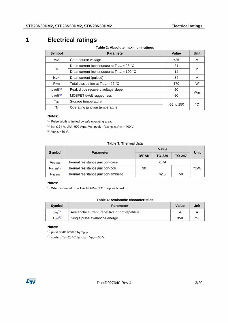
STB28N60DM2, STP28N60DM2, STW28N60DM2 Electrical ratings
DocID027040 Rev 4 3/20
1 Electrical ratings Table 2: Absolute maximum ratings
Symbol Parameter Value Unit
VGS Gate-source voltage ±25 V
ID Drain current (continuous) at Tcase = 25 °C 21
A Drain current (continuous) at Tcase = 100 °C 14
IDM(1) Drain current (pulsed) 84 A
PTOT Total dissipation at Tcase = 25 °C 170 W
dv/dt(2) Peak diode recovery voltage slope 50 V/ns
dv/dt(3) MOSFET dv/dt ruggedness 50
Tstg Storage temperature -55 to 150 °C
Tj Operating junction temperature
Notes:
(1) Pulse width is limited by safe operating area. (2) ISD ≤ 21 A, di/dt=900 A/μs; VDS peak < V(BR)DSS,VDD = 400 V (3) VDS ≤ 480 V.
Table 3: Thermal data
Symbol Parameter Value
Unit D²PAK TO-220 TO-247
Rthj-case Thermal resistance junction-case 0.74
°C/W Rthj-pcb(1) Thermal resistance junction-pcb 30
Rthj-amb Thermal resistance junction-ambient
62.5 50
Notes:
(1) When mounted on a 1-inch² FR-4, 2 Oz copper board.
Table 4: Avalanche characteristics
Symbol Parameter Value Unit
IAR(1) Avalanche current, repetitive or not repetitive 4 A
EAS(2) Single pulse avalanche energy 350 mJ
Notes:
(1) pulse width limited by Tjmax (2) starting Tj = 25 °C, ID = IAR, VDD = 50 V.
Electrical characteristics STB28N60DM2, STP28N60DM2, STW28N60DM2
4/20 DocID027040 Rev 4
2 Electrical characteristics
(Tcase = 25 °C unless otherwise specified)
Table 5: Static
Symbol Parameter Test conditions Min. Typ. Max. Unit
V(BR)DSS Drain-source breakdown
voltage VGS = 0 V, ID = 1 mA 600
V
IDSS Zero gate voltage drain
current
VGS = 0 V, VDS = 600 V
1
µA VGS = 0 V, VDS = 600 V,
Tcase = 125 °C 100
IGSS Gate-body leakage current VDS = 0 V, VGS = ±25 V
±10 µA
VGS(th) Gate threshold voltage VDS = VGS, ID = 250 µA 3 4 5 V
RDS(on) Static drain-source on-
resistance VGS = 10 V, ID = 10.5 A
0.13 0.16 Ω
Table 6: Dynamic
Symbol Parameter Test conditions Min. Typ. Max. Unit
Ciss Input capacitance
VDS = 100 V, f = 1 MHz,
VGS = 0 V
- 1500 -
pF Coss Output capacitance - 70 -
Crss Reverse transfer
capacitance - 1.6 -
Coss eq.(1)
Equivalent output
capacitance VDS = 0 to 480 V, VGS = 0 V - 134 - pF
RG Intrinsic gate resistance f = 1 MHz, ID = 0 A - 4.6 - Ω
Qg Total gate charge VDD = 480 V, ID = 21 A,
VGS = 10 V (see Figure 19:
"Test circuit for gate charge
behavior")
- 34 -
nC Qgs Gate-source charge - 8 -
Qgd Gate-drain charge - 18.5 -
Notes:
(1) Coss eq. is defined as a constant equivalent capacitance giving the same charging time as Coss when VDS
increases from 0 to 80% VDSS.
Table 7: Switching times
Symbol Parameter Test conditions Min. Typ. Max. Unit
td(on) Turn-on delay time VDD = 300 V, ID = 10.5 A
RG = 4.7 Ω, VGS = 10 V (see
Figure 18: "Test circuit for
resistive load switching times"
and Figure 23: "Switching time
waveform")
- 16 -
ns
tr Rise time - 7.3 -
td(off) Turn-off delay time - 53 -
tf Fall time - 9.3 -
STB28N60DM2, STP28N60DM2, STW28N60DM2 Electrical characteristics
DocID027040 Rev 4 5/20
Table 8: Source-drain diode
Symbol Parameter Test conditions Min. Typ. Max. Unit
ISD(1) Source-drain current
-
21 A
ISDM(2)
Source-drain current
(pulsed) -
84 A
VSD(3) Forward on voltage VGS = 0 V, ISD = 21 A -
1.6 V
trr Reverse recovery time ISD = 21 A, di/dt = 100 A/µs,
VDD = 60 V (see Figure 20:
"Test circuit for inductive load
switching and diode recovery
times")
- 140
ns
Qrr Reverse recovery charge - 0.5
µC
IRRM Reverse recovery current - 7.4
A
trr Reverse recovery time ISD = 21 A, di/dt = 100 A/µs,
VDD = 60 V, Tj = 150 °C (see
Figure 20: "Test circuit for
inductive load switching and
diode recovery times")
- 309
ns
Qrr Reverse recovery charge - 2.6
µC
IRRM Reverse recovery current - 16.8
A
Notes:
(1) Limited by maximum junction temperature. (2) Pulse width is limited by safe operating area. (3) Pulse test: pulse duration = 300 µs, duty cycle 1.5%.
Table 9: Gate-source Zener diode
Symbol Parameter Test conditions Min. Typ. Max. Unit
V(BR)GSO Gate-source breakdown voltage IGS = ±250 µA, ID = 0 A ±30 - - V
The built-in back-to-back Zener diodes are specifically designed to enhance the ESD performance of the device. The Zener voltage facilitates efficient and cost-effective device integrity protection, thus eliminating the need for additional external componentry.
Electrical characteristics STB28N60DM2, STP28N60DM2, STW28N60DM2
6/20 DocID027040 Rev 4
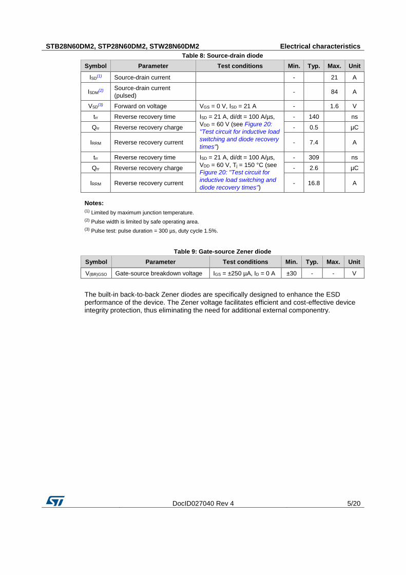
2.1 Electrical characteristics (curves)
Figure 2: Safe operating area for D²PAK
Figure 3: Thermal impedance for D²PAK
Figure 4: Safe operating area for TO-220
Figure 5: Thermal impedance for TO-220
Figure 6: Safe operating area for TO-247
Figure 7: Thermal impedance for TO-247
K
tpƬ
Zth= K*Rthj-cδ= tp/Ƭ
Single pulse
0.01
δ=0.5
10 -1
10 -2
10 -410 -5 10 -3 10 -2 10 -1 tP(s)
0.2
0.1
0.05
0.02
K
tpƬ
Zth= K*Rthj-cδ= tp/Ƭ
Single pulse
0.01
δ=0.5
10 -1
10 -2
10 -410 -5 10 -3 10 -2 10 -1 tP(s)
0.2
0.1
0.05
0.02
STB28N60DM2, STP28N60DM2, STW28N60DM2 Electrical characteristics
DocID027040 Rev 4 7/20
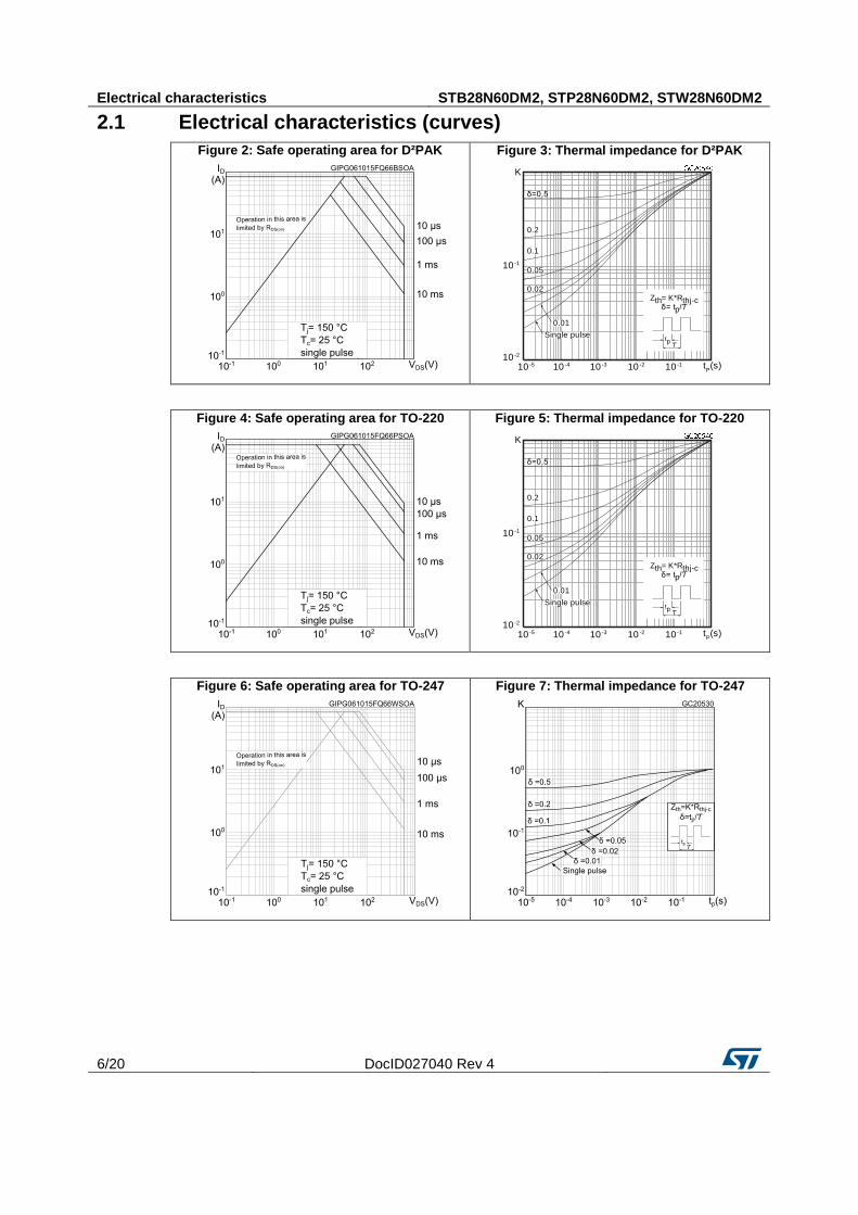
Figure 8: Output characteristics
Figure 9: Transfer characteristics
Figure 10: Gate charge vs gate-source voltage
Figure 11: Static drain-source on-resistance
Figure 12: Capacitance variations
Figure 13: Normalized gate threshold voltage vs temperature
Electrical characteristics STB28N60DM2, STP28N60DM2, STW28N60DM2
8/20 DocID027040 Rev 4
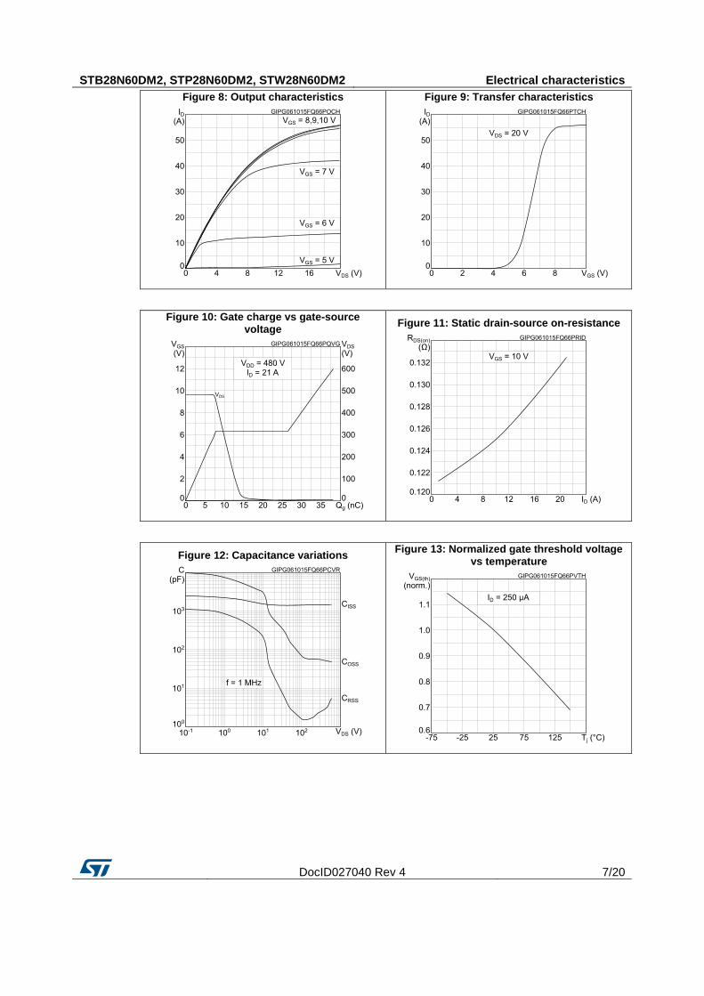
Figure 14: Normalized on-resistance vs temperature
Figure 15: Normalized V(BR)DSS vs temperature
Figure 16: Output capacitance stored energy
Figure 17: Source-drain diode forward characteristics
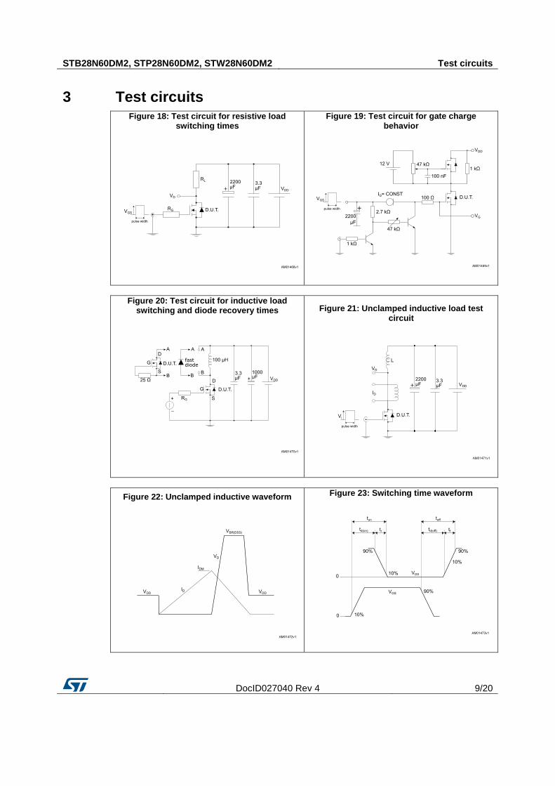
STB28N60DM2, STP28N60DM2, STW28N60DM2 Test circuits
DocID027040 Rev 4 9/20
3 Test circuits Figure 18: Test circuit for resistive load
switching times
Figure 19: Test circuit for gate charge behavior
Figure 20: Test circuit for inductive load switching and diode recovery times
Figure 21: Unclamped inductive load test circuit
Figure 22: Unclamped inductive waveform
Figure 23: Switching time waveform
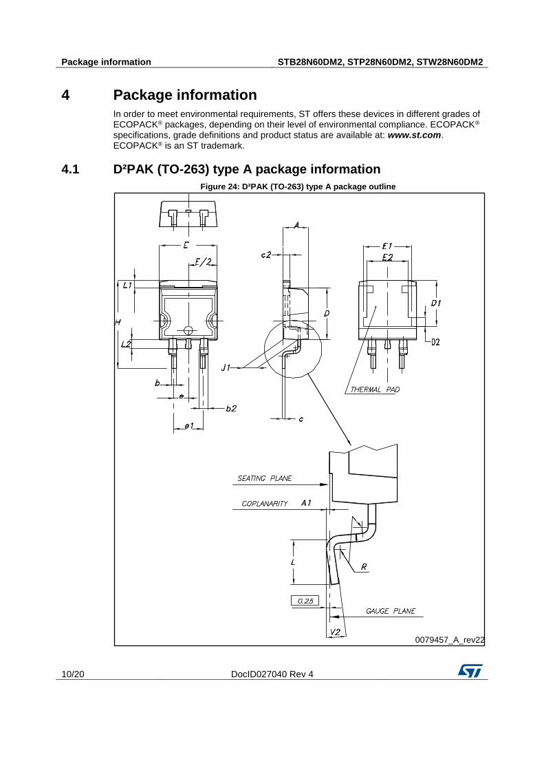
Package information STB28N60DM2, STP28N60DM2, STW28N60DM2
10/20 DocID027040 Rev 4
4 Package information
In order to meet environmental requirements, ST offers these devices in different grades of ECOPACK® packages, depending on their level of environmental compliance. ECOPACK® specifications, grade definitions and product status are available at: www.st.com. ECOPACK® is an ST trademark.
4.1 D²PAK (TO-263) type A package information
Figure 24: D²PAK (TO-263) type A package outline
0079457_A_rev22
STB28N60DM2, STP28N60DM2, STW28N60DM2 Package information
DocID027040 Rev 4 11/20
Table 10: D²PAK (TO-263) type A package mechanical data
Dim. mm
Min. Typ. Max.
A 4.40
4.60
A1 0.03
0.23
b 0.70
0.93
b2 1.14
1.70
c 0.45
0.60
c2 1.23
1.36
D 8.95
9.35
D1 7.50 7.75 8.00
D2 1.10 1.30 1.50
E 10
10.40
E1 8.50 8.70 8.90
E2 6.85 7.05 7.25
e
2.54
e1 4.88
5.28
H 15
15.85
J1 2.49
2.69
L 2.29
2.79
L1 1.27
1.40
L2 1.30
1.75
R
0.4
V2 0°
8°

Package information STB28N60DM2, STP28N60DM2, STW28N60DM2
12/20 DocID027040 Rev 4
Figure 25: D²PAK (TO-263) recommended footprint (dimensions are in mm)
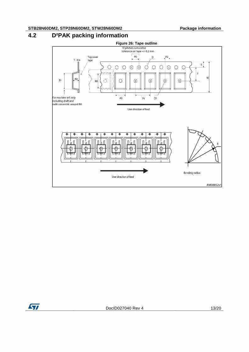
STB28N60DM2, STP28N60DM2, STW28N60DM2 Package information
DocID027040 Rev 4 13/20
4.2 D²PAK packing information
Figure 26: Tape outline
Package information STB28N60DM2, STP28N60DM2, STW28N60DM2
14/20 DocID027040 Rev 4
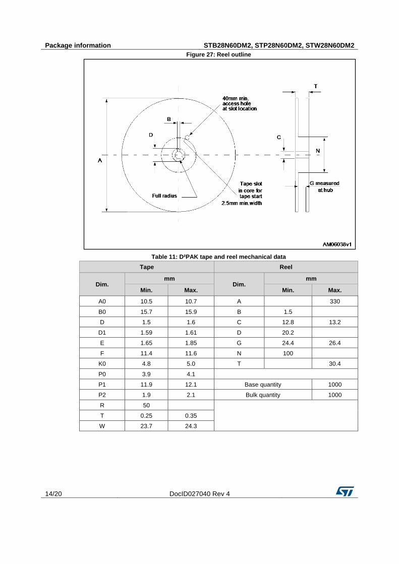
Figure 27: Reel outline
Table 11: D²PAK tape and reel mechanical data
Tape Reel
Dim. mm
Dim. mm
Min. Max. Min. Max.
A0 10.5 10.7 A
330
B0 15.7 15.9 B 1.5
D 1.5 1.6 C 12.8 13.2
D1 1.59 1.61 D 20.2
E 1.65 1.85 G 24.4 26.4
F 11.4 11.6 N 100
K0 4.8 5.0 T
30.4
P0 3.9 4.1
P1 11.9 12.1 Base quantity 1000
P2 1.9 2.1 Bulk quantity 1000
R 50
T 0.25 0.35
W 23.7 24.3
STB28N60DM2, STP28N60DM2, STW28N60DM2 Package information
DocID027040 Rev 4 15/20
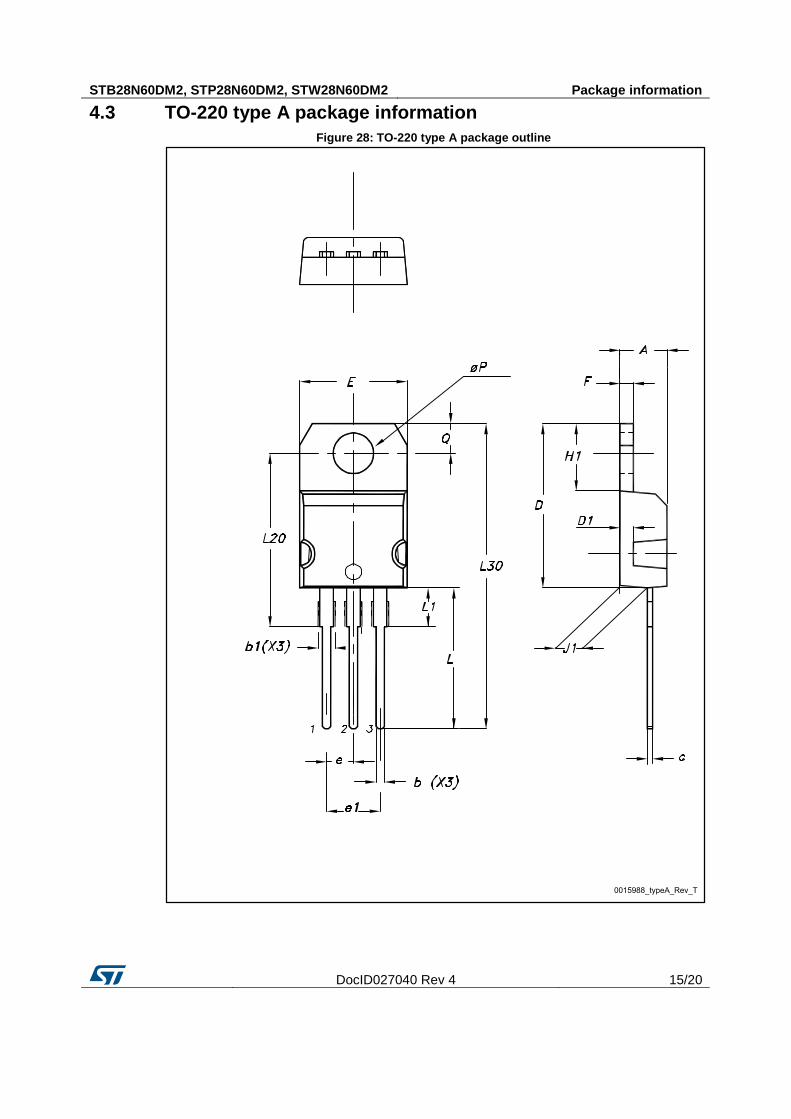
4.3 TO-220 type A package information
Figure 28: TO-220 type A package outline
Package information STB28N60DM2, STP28N60DM2, STW28N60DM2
16/20 DocID027040 Rev 4
Table 12: TO-220 type A mechanical data
Dim. mm
Min. Typ. Max.
A 4.40
4.60
b 0.61
0.88
b1 1.14
1.70
c 0.48
0.70
D 15.25
15.75
D1
1.27
E 10
10.40
e 2.40
2.70
e1 4.95
5.15
F 1.23
1.32
H1 6.20
6.60
J1 2.40
2.72
L 13
14
L1 3.50
3.93
L20
16.40
L30
28.90
øP 3.75
3.85
Q 2.65
2.95

STB28N60DM2, STP28N60DM2, STW28N60DM2 Package information
DocID027040 Rev 4 17/20
4.4 TO-247 package information
Figure 29: TO-247 package outline
Package information STB28N60DM2, STP28N60DM2, STW28N60DM2
18/20 DocID027040 Rev 4
Table 13: TO-247 package mechanical data
Dim. mm.
Min. Typ. Max.
A 4.85
5.15
A1 2.20
2.60
b 1.0
1.40
b1 2.0
2.40
b2 3.0
3.40
c 0.40
0.80
D 19.85
20.15
E 15.45
15.75
e 5.30 5.45 5.60
L 14.20
14.80
L1 3.70
4.30
L2
18.50
ØP 3.55
3.65
ØR 4.50
5.50
S 5.30 5.50 5.70
STB28N60DM2, STP28N60DM2, STW28N60DM2 Revision history
DocID027040 Rev 4 19/20
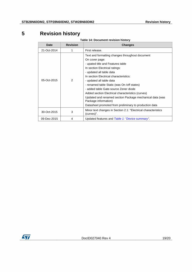
5 Revision history Table 14: Document revision history
Date Revision Changes
21-Oct-2014 1 First release.
05-Oct-2015 2
Text and formatting changes throughout document
On cover page:
- upated title and Features table
In section Electrical ratings:
- updated all table data
In section Electrical characteristics:
- updated all table data
- renamed table Static (was On /off states)
- added table Gate-source Zener diode
Added section Electrical characteristics (curves)
Updated and renamed section Package mechanical data (was
Package information)
Datasheet promoted from preliminary to production data
30-Oct-2015 3 Minor text changes in Section 2.1: "Electrical characteristics
(curves)".
09-Dec-2015 4 Updated features and Table 1: "Device summary".
STB28N60DM2, STP28N60DM2, STW28N60DM2
20/20 DocID027040 Rev 4
IMPORTANT NOTICE – PLEASE READ CAREFULLY
STMicroelectronics NV and its subsidiaries (“ST”) reserve the right to make changes, corrections, enhancements, modifications , and improvements to ST products and/or to this document at any time without notice. Purchasers should obtain the latest relevant information on ST products before placing orders. ST products are sold pursuant to ST’s terms and conditions of sale in place at the time of order acknowledgement.
Purchasers are solely responsible for the choice, selection, and use of ST products and ST assumes no liability for application assistance or the design of Purchasers’ products.
No license, express or implied, to any intellectual property right is granted by ST herein.
Resale of ST products with provisions different from the information set forth herein shall void any warranty granted by ST for such product.
ST and the ST logo are trademarks of ST. All other product or service names are the property of their respective owners.
Information in this document supersedes and replaces information previously supplied in any prior versions of this document.
© 2015 STMicroelectronics – All rights reserved