N-channel 600 V, 0.108 typ., 26 A MDmesh II Plus low … · DocID024298 Rev 2 5/19 STF33N60M2,...
19
This is information on a product in full production. November 2013 DocID024298 Rev 2 1/19 STF33N60M2, STI33N60M2, STP33N60M2, STW33N60M2 N-channel 600 V, 0.108 Ω typ., 26 A MDmesh II Plus™ low Q g Power MOSFETs in TO-220FP, I 2 PAK, TO-220 and TO-247 packages Datasheet - production data Figure 1. Internal schematic diagram Features • Extremely low gate charge • Lower R DS(on) x area vs previous generation • MDmesh™ II technology • Low gate input resistance • 100% avalanche tested • Zener-protected Applications • Switching applications • LCC converters, resonant converters Description These devices are N-channel Power MOSFETs developed using a new generation of MDmesh™ technology: MDmesh II Plus™ low Q g . These revolutionary Power MOSFETs associate a vertical structure to the company's strip layout to yield one of the world's lowest on-resistance and gate charge. They are therefore suitable for the most demanding high efficiency converters. TO-220 1 2 3 TAB TO-220FP 1 2 3 TO-247 1 2 3 1 2 3 TAB I PAK 2 AM15572v1 , TAB Order codes V DS @ T Jmax R DS(on) max I D STF33N60M2 650 V 0.125 Ω 26 A (1) 1. Limited by maximum junction temperature. STI33N60M2 26 A STP33N60M2 STW33N60M2 Table 1. Device summary Order codes Marking Package Packaging STF33N60M2 33N60M2 TO-220FP Tube STI33N60M2 I 2 PAK STP33N60M2 TO-220 STW33N60M2 TO-247 www.st.com
-
Upload
nguyenxuyen -
Category
Documents
-
view
214 -
download
0
Transcript of N-channel 600 V, 0.108 typ., 26 A MDmesh II Plus low … · DocID024298 Rev 2 5/19 STF33N60M2,...
This is information on a product in full production.
November 2013 DocID024298 Rev 2 1/19
STF33N60M2, STI33N60M2, STP33N60M2, STW33N60M2
N-channel 600 V, 0.108 Ω typ., 26 A MDmesh II Plus™ low Qg Power MOSFETs in TO-220FP, I2PAK, TO-220 and TO-247 packages
Datasheet - production data
Figure 1. Internal schematic diagram
Features
• Extremely low gate charge
• Lower RDS(on) x area vs previous generation
• MDmesh™ II technology
• Low gate input resistance
• 100% avalanche tested
• Zener-protected
Applications• Switching applications
• LCC converters, resonant converters
DescriptionThese devices are N-channel Power MOSFETs developed using a new generation of MDmesh™ technology: MDmesh II Plus™ low Qg. These revolutionary Power MOSFETs associate a vertical structure to the company's strip layout to yield one of the world's lowest on-resistance and gate charge. They are therefore suitable for the most demanding high efficiency converters.
TO-2201
23
TAB
TO-220FP
12
3
TO-247
12
31 2 3
TAB
I PAK2
AM15572v1
, TAB
Order codesVDS @ TJmax
RDS(on) max
ID
STF33N60M2
650 V 0.125 Ω
26 A(1)
1. Limited by maximum junction temperature.
STI33N60M2
26 ASTP33N60M2
STW33N60M2
Table 1. Device summary
Order codes Marking Package Packaging
STF33N60M2
33N60M2
TO-220FP
TubeSTI33N60M2 I2PAK
STP33N60M2 TO-220
STW33N60M2 TO-247
www.st.com
Contents STF33N60M2, STI33N60M2, STP33N60M2, STW33N60M2
2/19 DocID024298 Rev 2
Contents
1 Electrical ratings . . . . . . . . . . . . . . . . . . . . . . . . . . . . . . . . . . . . . . . . . . . . 3
2 Electrical characteristics . . . . . . . . . . . . . . . . . . . . . . . . . . . . . . . . . . . . . 4
2.1 Electrical characteristics (curves) . . . . . . . . . . . . . . . . . . . . . . . . . . . . . . . 6
3 Test circuits . . . . . . . . . . . . . . . . . . . . . . . . . . . . . . . . . . . . . . . . . . . . . . 9
4 Package mechanical data . . . . . . . . . . . . . . . . . . . . . . . . . . . . . . . . . . . . 10
5 Revision history . . . . . . . . . . . . . . . . . . . . . . . . . . . . . . . . . . . . . . . . . . . 18
DocID024298 Rev 2 3/19
STF33N60M2, STI33N60M2, STP33N60M2, STW33N60M2 Electrical ratings
19
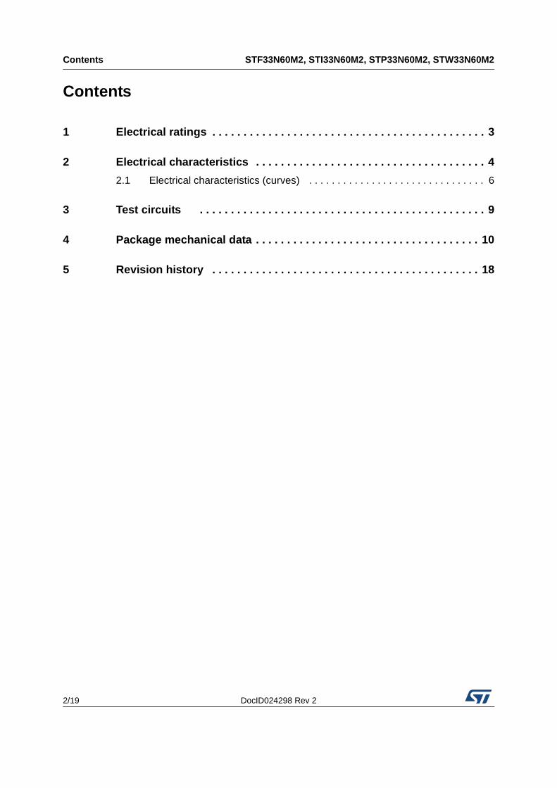
1 Electrical ratings
Table 2. Absolute maximum ratings
Symbol Parameter
Value
UnitI2PAK, TO-220
TO-247TO-220FP
VGS Gate-source voltage ± 25 V
ID Drain current (continuous) at TC = 25 °C 26 26(1)
1. Limited by maximum junction temperature.
A
ID Drain current (continuous) at TC = 100 °C 16 16(1) A
IDM (2)
2. Pulse width limited by safe operating area.
Drain current (pulsed) 104 104(1) A
PTOT Total dissipation at TC = 25 °C 190 35 W
dv/dt (3)
3. ISD ≤ 26 A, di/dt ≤ 400 A/µs; VDS peak < V(BR)DSS, VDD= 400 V.
Peak diode recovery voltage slope 15 V/ns
dv/dt(4)
4. VDS ≤ 480 V
MOSFET dv/dt ruggedness 50 V/ns
VISO
Insulation withstand voltage (RMS) from
all three leads to external heat sink(t = 1 s; TC = 25 °C)
2500 V
Tstg Storage temperature- 55 to 150 °C
Tj Max. operating junction temperature
Table 3. Thermal data
Symbol Parameter
Value
UnitTO-220FP
I2PAK, TO-220
TO-247
Rthj-case Thermal resistance junction-case max 3.6 0.66 °C/W
Rthj-amb Thermal resistance junction-ambient max 62.5 50 °C/W
Table 4. Avalanche characteristics
Symbol Parameter Value Unit
IARAvalanche current, repetitive or not repetitive (pulse width limited by Tjmax )
5 A
EASSingle pulse avalanche energy (starting Tj=25°C, ID= IAR; VDD=50)
2300 mJ
Electrical characteristics STF33N60M2, STI33N60M2, STP33N60M2, STW33N60M2
4/19 DocID024298 Rev 2
2 Electrical characteristics
(TC = 25 °C unless otherwise specified)
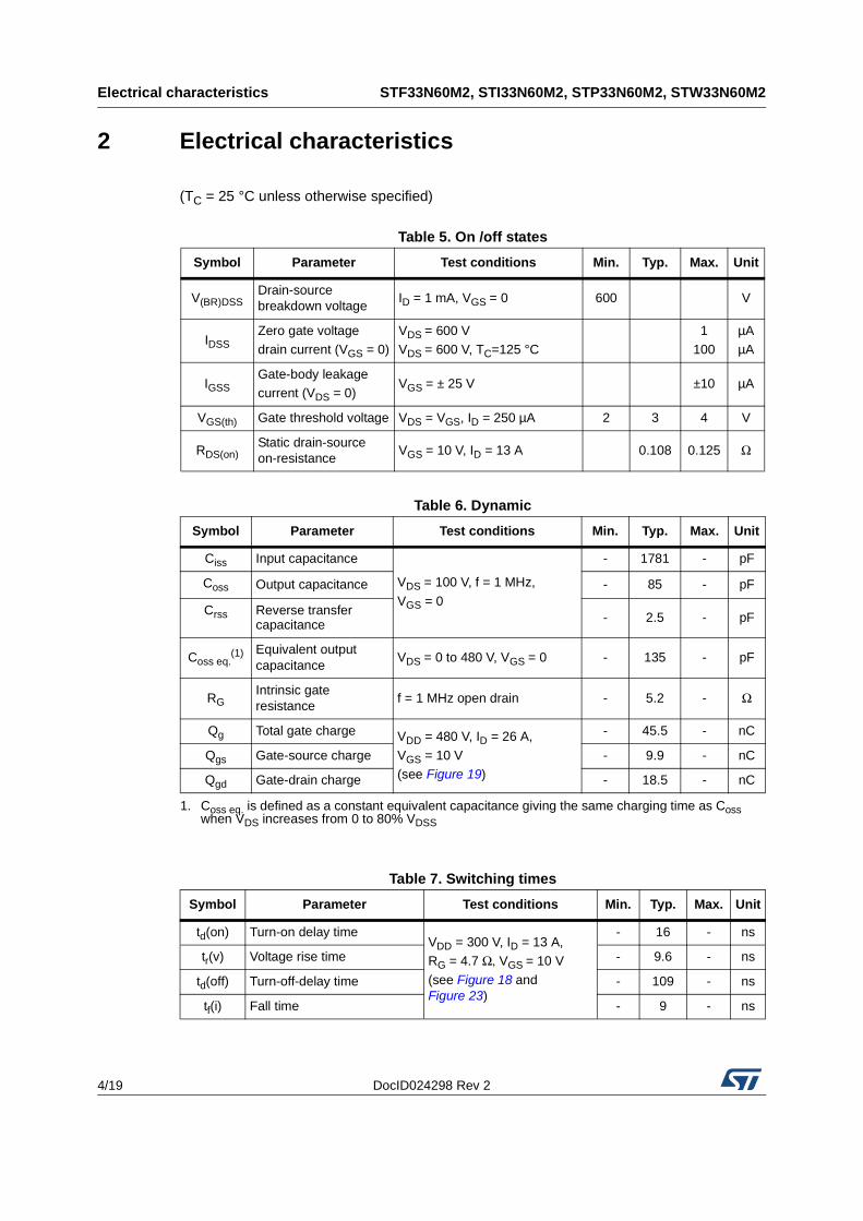
Table 5. On /off states
Symbol Parameter Test conditions Min. Typ. Max. Unit
V(BR)DSSDrain-source breakdown voltage
ID = 1 mA, VGS = 0 600 V
IDSSZero gate voltage drain current (VGS = 0)
VDS = 600 VVDS = 600 V, TC=125 °C
1100
µAµA
IGSSGate-body leakagecurrent (VDS = 0)
VGS = ± 25 V ±10 µA
VGS(th) Gate threshold voltage VDS = VGS, ID = 250 µA 2 3 4 V
RDS(on)Static drain-source on-resistance
VGS = 10 V, ID = 13 A 0.108 0.125 Ω
Table 6. Dynamic
Symbol Parameter Test conditions Min. Typ. Max. Unit
Ciss Input capacitance
VDS = 100 V, f = 1 MHz,
VGS = 0
- 1781 - pF
Coss Output capacitance - 85 - pF
Crss Reverse transfer capacitance - 2.5 - pF
Coss eq.(1)
1. Coss eq. is defined as a constant equivalent capacitance giving the same charging time as Coss when VDS increases from 0 to 80% VDSS
Equivalent output capacitance
VDS = 0 to 480 V, VGS = 0 - 135 - pF
RGIntrinsic gate resistance
f = 1 MHz open drain - 5.2 - Ω
Qg Total gate charge VDD = 480 V, ID = 26 A,
VGS = 10 V(see Figure 19)
- 45.5 - nC
Qgs Gate-source charge - 9.9 - nC
Qgd Gate-drain charge - 18.5 - nC
Table 7. Switching times
Symbol Parameter Test conditions Min. Typ. Max. Unit
td(on) Turn-on delay time VDD = 300 V, ID = 13 A, RG = 4.7 Ω, VGS = 10 V
(see Figure 18 and Figure 23)
- 16 - ns
tr(v) Voltage rise time - 9.6 - ns
td(off) Turn-off-delay time - 109 - ns
tf(i) Fall time - 9 - ns
DocID024298 Rev 2 5/19
STF33N60M2, STI33N60M2, STP33N60M2, STW33N60M2 Electrical characteristics
19
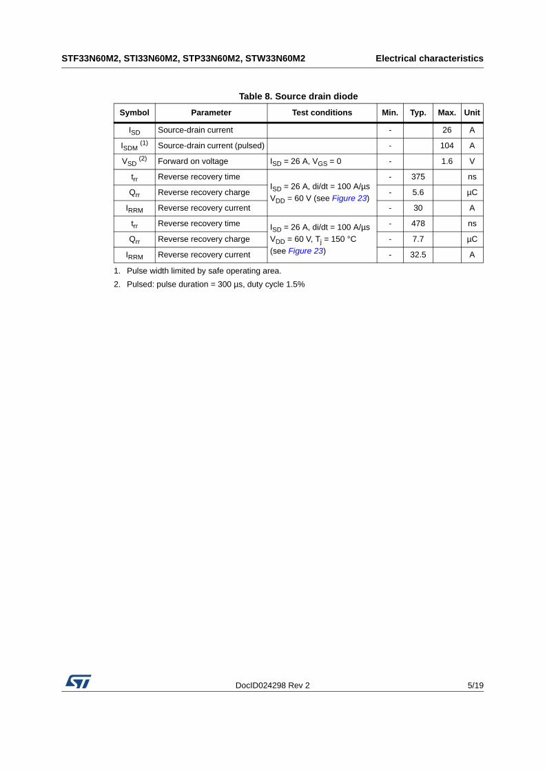
Table 8. Source drain diode
Symbol Parameter Test conditions Min. Typ. Max. Unit
ISD Source-drain current - 26 A
ISDM (1)
1. Pulse width limited by safe operating area.
Source-drain current (pulsed) - 104 A
VSD (2)
2. Pulsed: pulse duration = 300 µs, duty cycle 1.5%
Forward on voltage ISD = 26 A, VGS = 0 - 1.6 V
trr Reverse recovery timeISD = 26 A, di/dt = 100 A/µsVDD = 60 V (see Figure 23)
- 375 ns
Qrr Reverse recovery charge - 5.6 µC
IRRM Reverse recovery current - 30 A
trr Reverse recovery time ISD = 26 A, di/dt = 100 A/µsVDD = 60 V, Tj = 150 °C(see Figure 23)
- 478 ns
Qrr Reverse recovery charge - 7.7 µC
IRRM Reverse recovery current - 32.5 A
Electrical characteristics STF33N60M2, STI33N60M2, STP33N60M2, STW33N60M2
6/19 DocID024298 Rev 2
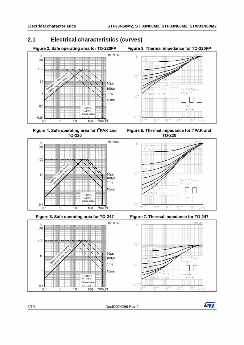
2.1 Electrical characteristics (curves)
Figure 2. Safe operating area for TO-220FP Figure 3. Thermal impedance for TO-220FP
ID
1
0.1
0.1 1 100 VDS(V)10
(A)
Operation in
this
area is
Limite
d by m
ax RDS(on)
10µs
100µs
1ms
10ms
0.01
Tj=150°CTc=25°CSingle pulse
10
100
AM17917v1
Figure 4. Safe operating area for I2PAK and TO-220
Figure 5. Thermal impedance for I2PAK and TO-220
Figure 6. Safe operating area for TO-247 Figure 7. Thermal impedance for TO-247
ID
10
1
0.1 1 100 VDS(V)10
(A)
Opera
tion
in th
is ar
ea is
Limite
d by
max
RDS(o
n)
10µs100µs1ms
10ms
0.1
Tj=150°CTc=25°CSingle pulse
100
AM17906v1
ID
10
1
0.1 1 100 VDS(V)10
(A)
Opera
tion
in th
is ar
ea is
Limite
d by
max
RDS(o
n)
10µs100µs
1ms
10ms
0.1
Tj=150°CTc=25°CSingle pulse
100
AM17918v1
DocID024298 Rev 2 7/19
STF33N60M2, STI33N60M2, STP33N60M2, STW33N60M2 Electrical characteristics
19
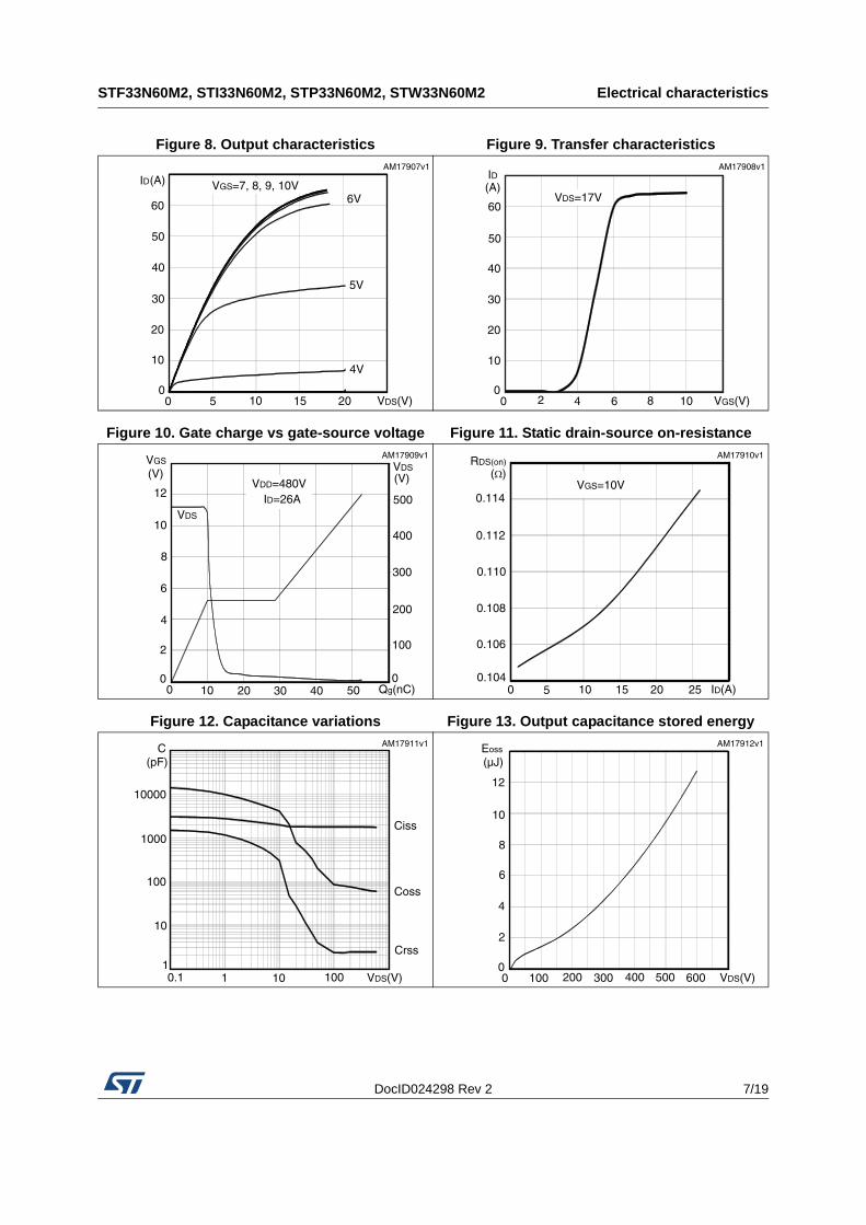
Figure 8. Output characteristics Figure 9. Transfer characteristics
Figure 10. Gate charge vs gate-source voltage Figure 11. Static drain-source on-resistance
Figure 12. Capacitance variations Figure 13. Output capacitance stored energy
ID
50
30
10
00 5 VDS(V)10
(A)
15
4V
5V
VGS=7, 8, 9, 10V
20
40
606V
20
AM17907v1ID
60
40
20
00 4 VGS(V)8
(A)
2 6 10
10
30
50
VDS=17V
AM17908v1
VGS
6
4
2
00 20 Qg(nC)
(V)
8
30 40
10
VDD=480VID=26A12
300
200
100
0
400
500VDS
10 50
VDS(V)
AM17909v1RDS(on)
0.108
0.106
0.1040 10 ID(A)
(Ω)
5 15
0.110
VGS=10V
20 25
0.112
0.114
AM17910v1
C
1000
100
10
10.1 10 VDS(V)
(pF)
1 100
Ciss
Coss
Crss
10000
AM17911v1 Eoss
4
2
00 100 VDS(V)
(µJ)
400200 300
6
500 600
8
10
12
AM17912v1
Electrical characteristics STF33N60M2, STI33N60M2, STP33N60M2, STW33N60M2
8/19 DocID024298 Rev 2
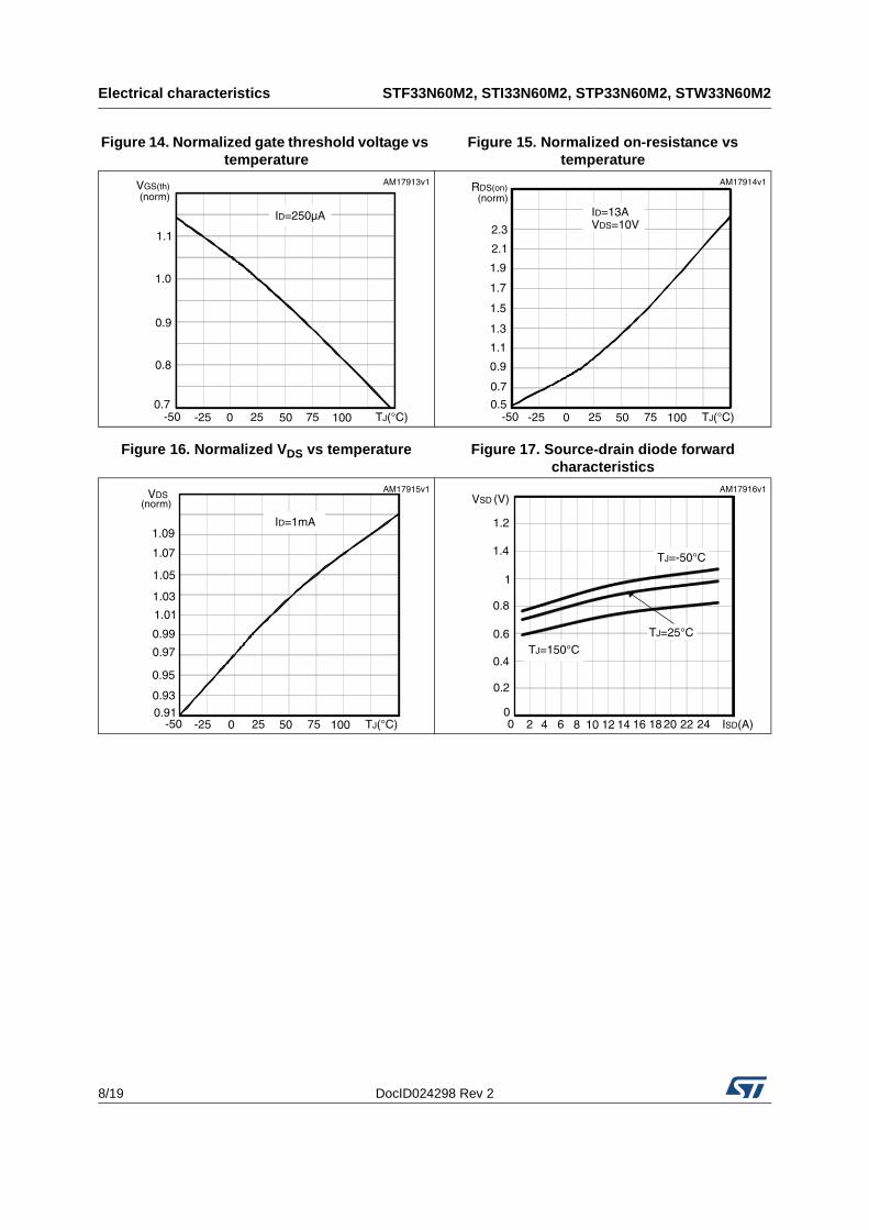
Figure 14. Normalized gate threshold voltage vs temperature
Figure 15. Normalized on-resistance vs temperature
Figure 16. Normalized VDS vs temperature Figure 17. Source-drain diode forward characteristics
VGS(th)
1.0
0.9
0.8
0.7-50 0 TJ(°C)
(norm)
-25
1.1
7525 50 100
ID=250µA
AM17913v1 RDS(on)
1.9
1.3
0.9
0.5-50 0 TJ(°C)
(norm)
-25 7525 50 100
0.7
1.1
1.5
1.7
2.1
2.3
ID=13AVDS=10V
AM17914v1
VDS
-50 0 TJ(°C)
(norm)
-25 7525 50 1000.91
0.93
0.95
0.97
0.99
1.01
1.03
1.05
ID=1mA
1.07
1.09
AM17915v1VSD
0 4 ISD(A)
(V)
2 106 80
0.2
0.4
0.6
TJ=-50°C
TJ=150°C
TJ=25°C
0.8
1
12 14 16 18 20 22 24
1.2
1.4
AM17916v1
DocID024298 Rev 2 9/19
STF33N60M2, STI33N60M2, STP33N60M2, STW33N60M2 Test circuits
19
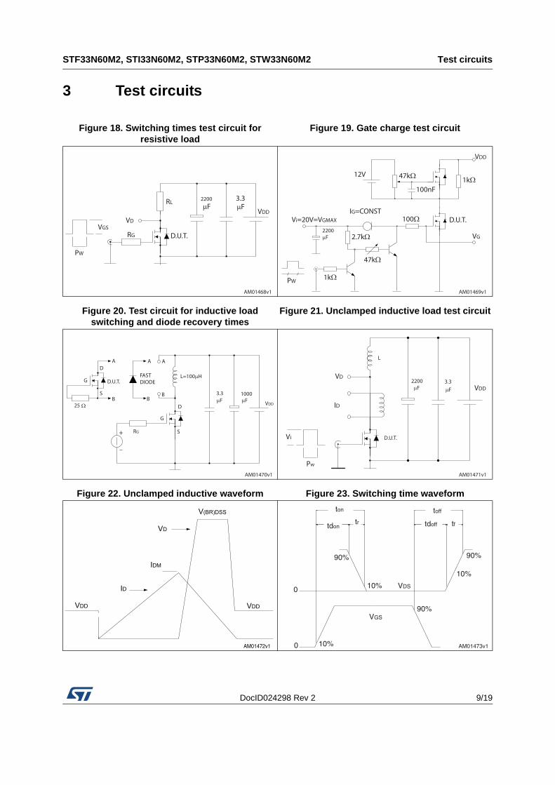
3 Test circuits
Figure 18. Switching times test circuit for resistive load
Figure 19. Gate charge test circuit
Figure 20. Test circuit for inductive load switching and diode recovery times
Figure 21. Unclamped inductive load test circuit
Figure 22. Unclamped inductive waveform Figure 23. Switching time waveform
AM01468v1
VGS
PW
VD
RG
RL
D.U.T.
2200
μF3.3μF
VDD
AM01469v1
VDD
47kΩ 1kΩ
47kΩ
2.7kΩ
1kΩ
12V
Vi=20V=VGMAX
2200μF
PW
IG=CONST100Ω
100nF
D.U.T.
VG
AM01470v1
AD
D.U.T.
SB
G
25 Ω
A A
BB
RG
G
FASTDIODE
D
S
L=100μH
μF3.3 1000
μF VDD
AM01471v1
Vi
Pw
VD
ID
D.U.T.
L
2200μF
3.3μF VDD
AM01473v1
VDS
ton
tdon tdoff
toff
tftr
90%
10%
10%
0
0
90%
90%
10%
VGS
Package mechanical data STF33N60M2, STI33N60M2, STP33N60M2, STW33N60M2
10/19 DocID024298 Rev 2
4 Package mechanical data
In order to meet environmental requirements, ST offers these devices in different grades of ECOPACK® packages, depending on their level of environmental compliance. ECOPACK® specifications, grade definitions and product status are available at: www.st.com. ECOPACK® is an ST trademark.
DocID024298 Rev 2 11/19
STF33N60M2, STI33N60M2, STP33N60M2, STW33N60M2 Package mechanical data
19
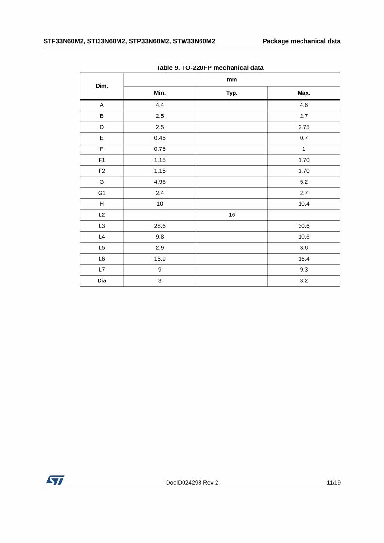
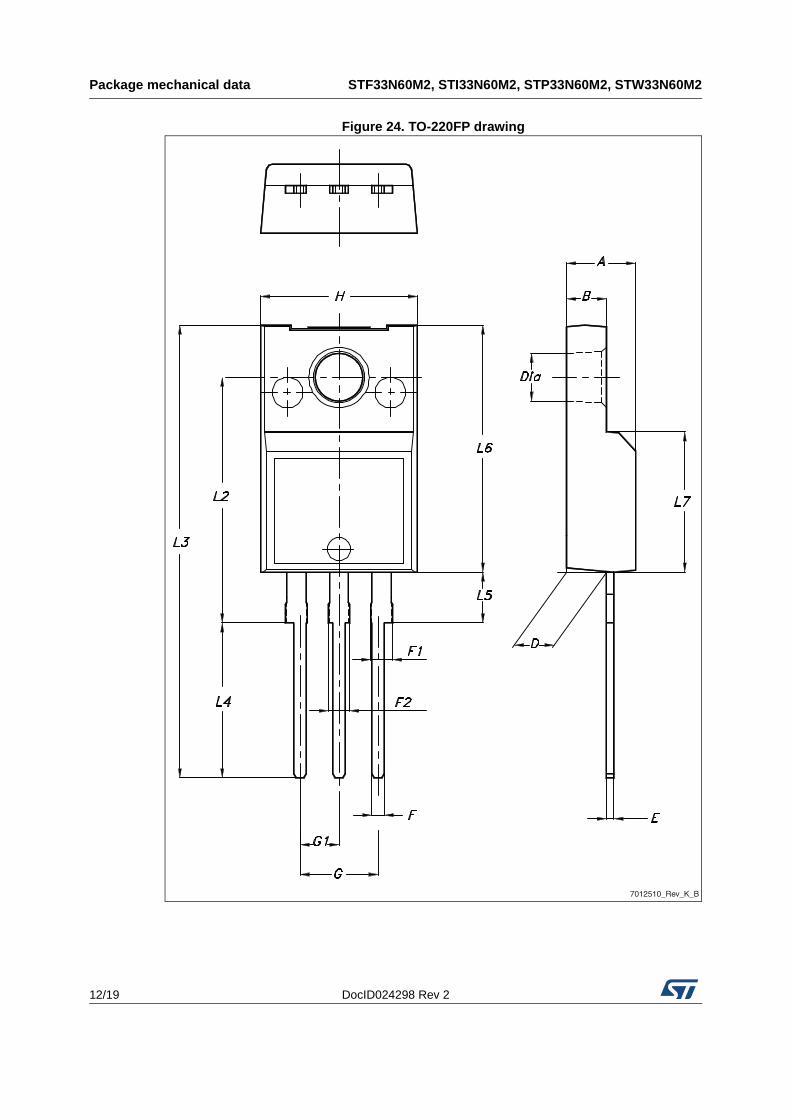
Table 9. TO-220FP mechanical data
Dim.mm
Min. Typ. Max.
A 4.4 4.6
B 2.5 2.7
D 2.5 2.75
E 0.45 0.7
F 0.75 1
F1 1.15 1.70
F2 1.15 1.70
G 4.95 5.2
G1 2.4 2.7
H 10 10.4
L2 16
L3 28.6 30.6
L4 9.8 10.6
L5 2.9 3.6
L6 15.9 16.4
L7 9 9.3
Dia 3 3.2
Package mechanical data STF33N60M2, STI33N60M2, STP33N60M2, STW33N60M2
12/19 DocID024298 Rev 2
Figure 24. TO-220FP drawing
7012510_Rev_K_B
DocID024298 Rev 2 13/19
STF33N60M2, STI33N60M2, STP33N60M2, STW33N60M2 Package mechanical data
19
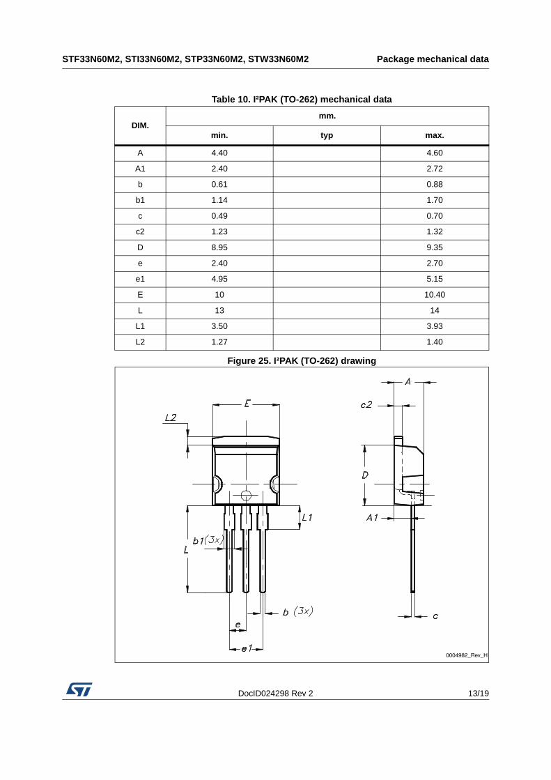
Figure 25. I²PAK (TO-262) drawing
Table 10. I²PAK (TO-262) mechanical data
DIM.mm.
min. typ max.
A 4.40 4.60
A1 2.40 2.72
b 0.61 0.88
b1 1.14 1.70
c 0.49 0.70
c2 1.23 1.32
D 8.95 9.35
e 2.40 2.70
e1 4.95 5.15
E 10 10.40
L 13 14
L1 3.50 3.93
L2 1.27 1.40
0004982_Rev_H
Package mechanical data STF33N60M2, STI33N60M2, STP33N60M2, STW33N60M2
14/19 DocID024298 Rev 2
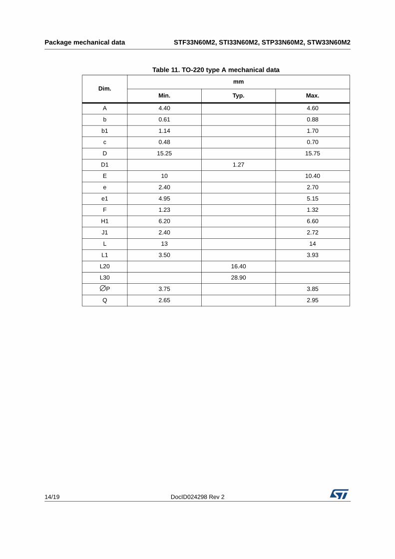
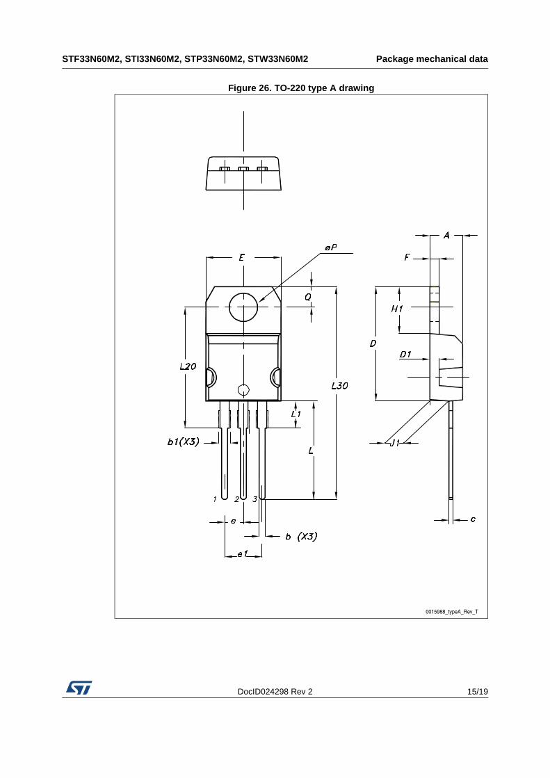
Table 11. TO-220 type A mechanical data
Dim.mm
Min. Typ. Max.
A 4.40 4.60
b 0.61 0.88
b1 1.14 1.70
c 0.48 0.70
D 15.25 15.75
D1 1.27
E 10 10.40
e 2.40 2.70
e1 4.95 5.15
F 1.23 1.32
H1 6.20 6.60
J1 2.40 2.72
L 13 14
L1 3.50 3.93
L20 16.40
L30 28.90
∅P 3.75 3.85
Q 2.65 2.95
DocID024298 Rev 2 15/19
STF33N60M2, STI33N60M2, STP33N60M2, STW33N60M2 Package mechanical data
19
Figure 26. TO-220 type A drawing
Package mechanical data STF33N60M2, STI33N60M2, STP33N60M2, STW33N60M2
16/19 DocID024298 Rev 2
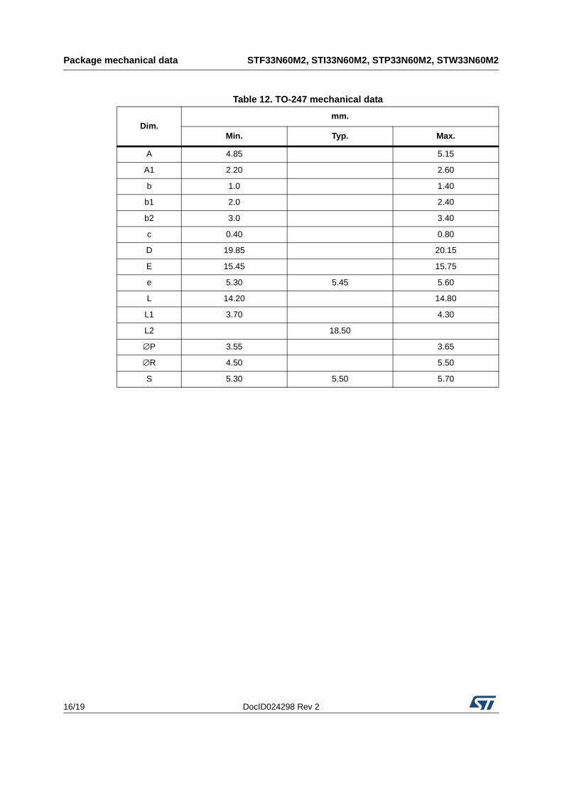
Table 12. TO-247 mechanical data
Dim.mm.
Min. Typ. Max.
A 4.85 5.15
A1 2.20 2.60
b 1.0 1.40
b1 2.0 2.40
b2 3.0 3.40
c 0.40 0.80
D 19.85 20.15
E 15.45 15.75
e 5.30 5.45 5.60
L 14.20 14.80
L1 3.70 4.30
L2 18.50
∅P 3.55 3.65
∅R 4.50 5.50
S 5.30 5.50 5.70
DocID024298 Rev 2 17/19
STF33N60M2, STI33N60M2, STP33N60M2, STW33N60M2 Package mechanical data
19
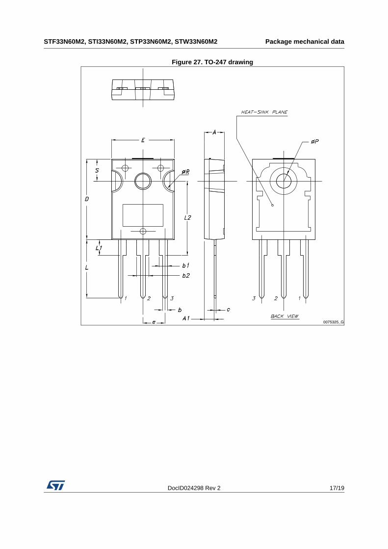
Figure 27. TO-247 drawing
0075325_G
Revision history STF33N60M2, STI33N60M2, STP33N60M2, STW33N60M2
18/19 DocID024298 Rev 2
5 Revision history
Table 13. Document revision history
Date Revision Changes
13-Sep-2013 1 First release.
19-Nov-2013 2
– Modified: RDS(on) and ID values in cover page– Modified: values in Table 4– Modified: RDS(on) typical and maximum values in Table 5, the
entire typical values in Table 6, 7 and 8– Added: Section 2.1: Electrical characteristics (curves)
– Minor text changes
DocID024298 Rev 2 19/19
STF33N60M2, STI33N60M2, STP33N60M2, STW33N60M2
19
Please Read Carefully:
Information in this document is provided solely in connection with ST products. STMicroelectronics NV and its subsidiaries (“ST”) reserve theright to make changes, corrections, modifications or improvements, to this document, and the products and services described herein at anytime, without notice.
All ST products are sold pursuant to ST’s terms and conditions of sale.
Purchasers are solely responsible for the choice, selection and use of the ST products and services described herein, and ST assumes noliability whatsoever relating to the choice, selection or use of the ST products and services described herein.
No license, express or implied, by estoppel or otherwise, to any intellectual property rights is granted under this document. If any part of thisdocument refers to any third party products or services it shall not be deemed a license grant by ST for the use of such third party productsor services, or any intellectual property contained therein or considered as a warranty covering the use in any manner whatsoever of suchthird party products or services or any intellectual property contained therein.
UNLESS OTHERWISE SET FORTH IN ST’S TERMS AND CONDITIONS OF SALE ST DISCLAIMS ANY EXPRESS OR IMPLIEDWARRANTY WITH RESPECT TO THE USE AND/OR SALE OF ST PRODUCTS INCLUDING WITHOUT LIMITATION IMPLIEDWARRANTIES OF MERCHANTABILITY, FITNESS FOR A PARTICULAR PURPOSE (AND THEIR EQUIVALENTS UNDER THE LAWSOF ANY JURISDICTION), OR INFRINGEMENT OF ANY PATENT, COPYRIGHT OR OTHER INTELLECTUAL PROPERTY RIGHT.
ST PRODUCTS ARE NOT DESIGNED OR AUTHORIZED FOR USE IN: (A) SAFETY CRITICAL APPLICATIONS SUCH AS LIFESUPPORTING, ACTIVE IMPLANTED DEVICES OR SYSTEMS WITH PRODUCT FUNCTIONAL SAFETY REQUIREMENTS; (B)AERONAUTIC APPLICATIONS; (C) AUTOMOTIVE APPLICATIONS OR ENVIRONMENTS, AND/OR (D) AEROSPACE APPLICATIONSOR ENVIRONMENTS. WHERE ST PRODUCTS ARE NOT DESIGNED FOR SUCH USE, THE PURCHASER SHALL USE PRODUCTS ATPURCHASER’S SOLE RISK, EVEN IF ST HAS BEEN INFORMED IN WRITING OF SUCH USAGE, UNLESS A PRODUCT ISEXPRESSLY DESIGNATED BY ST AS BEING INTENDED FOR “AUTOMOTIVE, AUTOMOTIVE SAFETY OR MEDICAL” INDUSTRYDOMAINS ACCORDING TO ST PRODUCT DESIGN SPECIFICATIONS. PRODUCTS FORMALLY ESCC, QML OR JAN QUALIFIED AREDEEMED SUITABLE FOR USE IN AEROSPACE BY THE CORRESPONDING GOVERNMENTAL AGENCY.
Resale of ST products with provisions different from the statements and/or technical features set forth in this document shall immediately voidany warranty granted by ST for the ST product or service described herein and shall not create or extend in any manner whatsoever, anyliability of ST.
ST and the ST logo are trademarks or registered trademarks of ST in various countries.Information in this document supersedes and replaces all information previously supplied.
The ST logo is a registered trademark of STMicroelectronics. All other names are the property of their respective owners.
© 2013 STMicroelectronics - All rights reserved
STMicroelectronics group of companies
Australia - Belgium - Brazil - Canada - China - Czech Republic - Finland - France - Germany - Hong Kong - India - Israel - Italy - Japan - Malaysia - Malta - Morocco - Philippines - Singapore - Spain - Sweden - Switzerland - United Kingdom - United States of America
www.st.com