N-channel 60 V, 0.0024 , 120 A STripFET VI … · PW IG=CONST 100 Ω 100nF D.U.T. VG AM01470v1 A D...
14
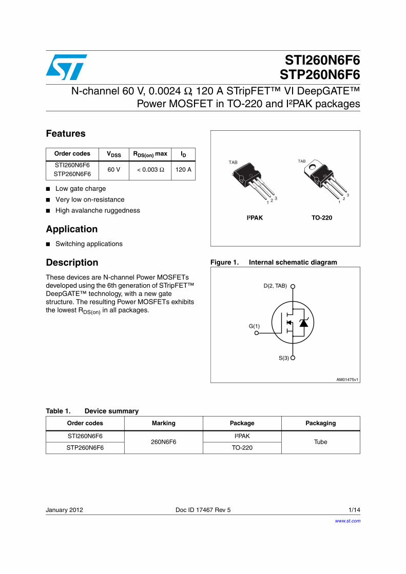
January 2012 Doc ID 17467 Rev 5 1/14 14 STI260N6F6 STP260N6F6 N-channel 60 V, 0.0024 Ω , 120 A STripFET™ VI DeepGATE™ Power MOSFET in TO-220 and I²PAK packages Features ■ Low gate charge ■ Very low on-resistance ■ High avalanche ruggedness Application ■ Switching applications Description These devices are N-channel Power MOSFETs developed using the 6th generation of STripFET™ DeepGATE™ technology, with a new gate structure. The resulting Power MOSFETs exhibits the lowest R DS(on) in all packages. Figure 1. Internal schematic diagram Order codes V DSS R DS(on) max I D STI260N6F6 STP260N6F6 60 V < 0.003 Ω 120 A TO-220 I²PAK 1 2 3 TAB 1 2 3 TAB Table 1. Device summary Order codes Marking Package Packaging STI260N6F6 260N6F6 I²PAK Tube STP260N6F6 TO-220 www.st.com
Transcript of N-channel 60 V, 0.0024 , 120 A STripFET VI … · PW IG=CONST 100 Ω 100nF D.U.T. VG AM01470v1 A D...
January 2012 Doc ID 17467 Rev 5 1/14
14
STI260N6F6STP260N6F6
N-channel 60 V, 0.0024 Ω, 120 A STripFET™ VI DeepGATE™Power MOSFET in TO-220 and I²PAK packages
Features
■ Low gate charge
■ Very low on-resistance
■ High avalanche ruggedness
Application■ Switching applications
DescriptionThese devices are N-channel Power MOSFETs developed using the 6th generation of STripFET™ DeepGATE™ technology, with a new gate structure. The resulting Power MOSFETs exhibits the lowest RDS(on) in all packages.
Figure 1. Internal schematic diagram
Order codes VDSS RDS(on) max ID
STI260N6F6
STP260N6F660 V < 0.003 Ω 120 A
TO-220I²PAK
1 2 3
TAB
12
3
TAB
Table 1. Device summary
Order codes Marking Package Packaging
STI260N6F6260N6F6
I²PAKTube
STP260N6F6 TO-220
www.st.com
Contents STI260N6F6, STP260N6F6
2/14 Doc ID 17467 Rev 5
Contents
1 Electrical ratings . . . . . . . . . . . . . . . . . . . . . . . . . . . . . . . . . . . . . . . . . . . . 3
2 Electrical characteristics . . . . . . . . . . . . . . . . . . . . . . . . . . . . . . . . . . . . . 4
2.1 Electrical characteristics (curves) . . . . . . . . . . . . . . . . . . . . . . . . . . . . . 6
3 Test circuits . . . . . . . . . . . . . . . . . . . . . . . . . . . . . . . . . . . . . . . . . . . . . . 8
4 Package mechanical data . . . . . . . . . . . . . . . . . . . . . . . . . . . . . . . . . . . . . 9
5 Revision history . . . . . . . . . . . . . . . . . . . . . . . . . . . . . . . . . . . . . . . . . . . 13
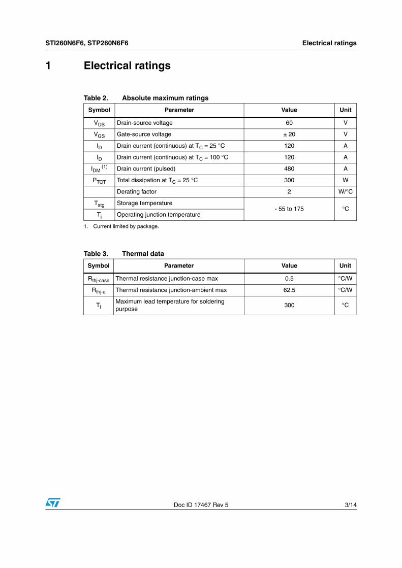
STI260N6F6, STP260N6F6 Electrical ratings
Doc ID 17467 Rev 5 3/14
1 Electrical ratings
Table 2. Absolute maximum ratings
Symbol Parameter Value Unit
VDS Drain-source voltage 60 V
VGS Gate-source voltage ± 20 V
ID Drain current (continuous) at TC = 25 °C 120 A
ID Drain current (continuous) at TC = 100 °C 120 A
IDM (1)
1. Current limited by package.
Drain current (pulsed) 480 A
PTOT Total dissipation at TC = 25 °C 300 W
Derating factor 2 W/°C
Tstg Storage temperature- 55 to 175 °C
Tj Operating junction temperature
Table 3. Thermal data
Symbol Parameter Value Unit
Rthj-case Thermal resistance junction-case max 0.5 °C/W
Rthj-a Thermal resistance junction-ambient max 62.5 °C/W
TlMaximum lead temperature for soldering purpose
300 °C
Electrical characteristics STI260N6F6, STP260N6F6
4/14 Doc ID 17467 Rev 5
2 Electrical characteristics
(TCASE = 25 °C unless otherwise specified)
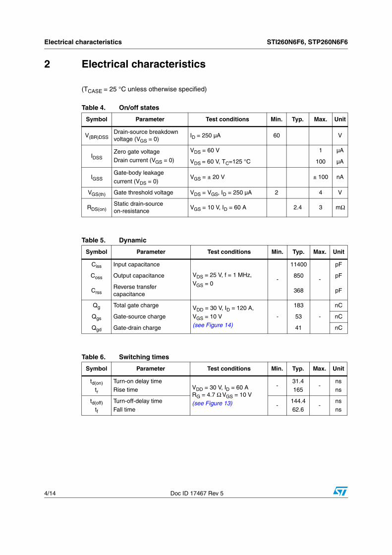
Table 4. On/off states
Symbol Parameter Test conditions Min. Typ. Max. Unit
V(BR)DSSDrain-source breakdown voltage (VGS = 0)
ID = 250 µA 60 V
IDSSZero gate voltage Drain current (VGS = 0)
VDS = 60 V 1 µA
VDS = 60 V, TC=125 °C 100 µA
IGSSGate-body leakage
current (VDS = 0)VGS = ± 20 V ± 100 nA
VGS(th) Gate threshold voltage VDS = VGS, ID = 250 µA 2 4 V
RDS(on)Static drain-source on-resistance
VGS = 10 V, ID = 60 A 2.4 3 mΩ
Table 5. Dynamic
Symbol Parameter Test conditions Min. Typ. Max. Unit
Ciss Input capacitance
VDS = 25 V, f = 1 MHz, VGS = 0
-
11400
-
pF
Coss Output capacitance 850 pF
CrssReverse transfer capacitance
368 pF
Qg Total gate charge VDD = 30 V, ID = 120 A,VGS = 10 V(see Figure 14)
-
183
-
nC
Qgs Gate-source charge 53 nC
Qgd Gate-drain charge 41 nC
Table 6. Switching times
Symbol Parameter Test conditions Min. Typ. Max. Unit
td(on)
tr
Turn-on delay time Rise time VDD = 30 V, ID = 60 A
RG = 4.7 Ω VGS = 10 V(see Figure 13)
-31.4165
-nsns
td(off)
tf
Turn-off-delay timeFall time
-144.462.6
-nsns
STI260N6F6, STP260N6F6 Electrical characteristics
Doc ID 17467 Rev 5 5/14
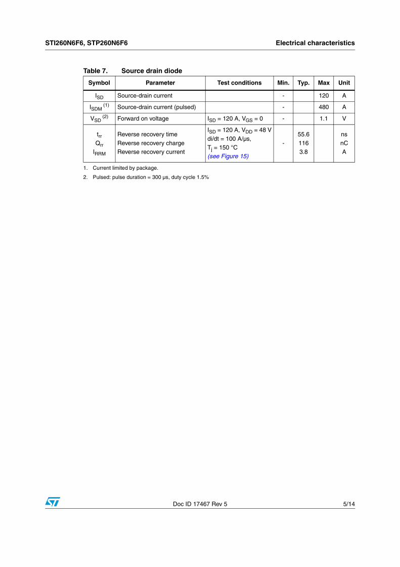
Table 7. Source drain diode
Symbol Parameter Test conditions Min. Typ. Max Unit
ISD Source-drain current - 120 A
ISDM (1)
1. Current limited by package.
Source-drain current (pulsed) - 480 A
VSD (2)
2. Pulsed: pulse duration = 300 µs, duty cycle 1.5%
Forward on voltage ISD = 120 A, VGS = 0 - 1.1 V
trrQrr
IRRM
Reverse recovery time
Reverse recovery chargeReverse recovery current
ISD = 120 A, VDD = 48 V
di/dt = 100 A/µs,Tj = 150 °C(see Figure 15)
-
55.6
1163.8
ns
nCA
Electrical characteristics STI260N6F6, STP260N6F6
6/14 Doc ID 17467 Rev 5
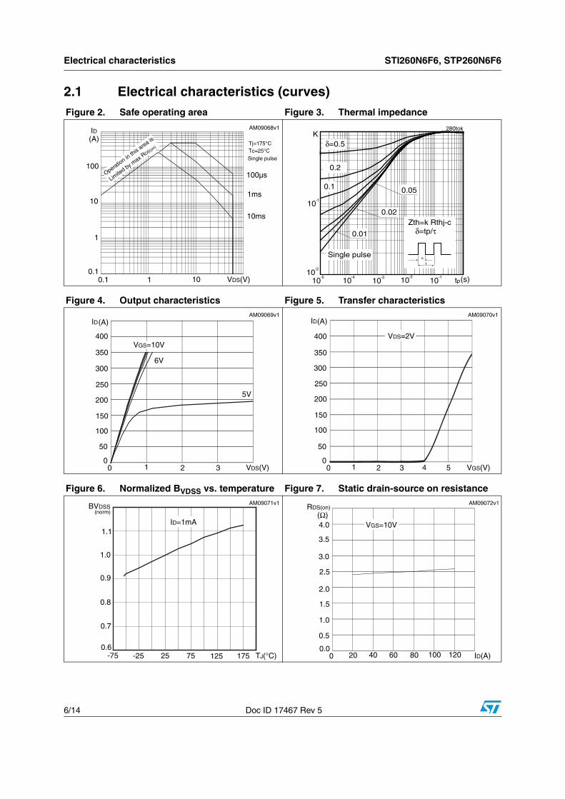
2.1 Electrical characteristics (curves) Figure 2. Safe operating area Figure 3. Thermal impedance
Figure 4. Output characteristics Figure 5. Transfer characteristics
Figure 6. Normalized BVDSS vs. temperature Figure 7. Static drain-source on resistance
ID
100
10
1
0.10.1 1 VDS(V)10
(A)
Operation in
this
area is
Limite
d by max R
DS(on)
100µs
1ms
10ms
Tj=175°CTc=25°CSingle pulse
AM09068v1
10-5
10-4
10-3 10
-210
-1tp(s)
10-2
10-1
K
0.2
0.05
0.02
0.01
0.1
Zth=k Rthj-cδ=tp/τ
tp
τ
Single pulse
δ=0.5
280tok
ID
150
100
50
00 2 VDS(V)
(A)
1 3
200
2505V
6V
VGS=10V
300
350
400
AM09069v1ID
150
100
50
00 2 VGS(V)4
(A)
1 3 5
200
250
300
350
400 VDS=2V
AM09070v1
BVDSS
-75 TJ(°C)
(norm)
-25 7525 1250.6
0.7
0.8
0.9
1.0
1.1
175
ID=1mA
AM09071v1RDS(on)
1.5
1.0
0.5
0.00 40 ID(A)
(Ω)
20 60
2.0
2.5
3.0
3.5
VGS=10V
10080 120
4.0
AM09072v1
STI260N6F6, STP260N6F6 Electrical characteristics
Doc ID 17467 Rev 5 7/14
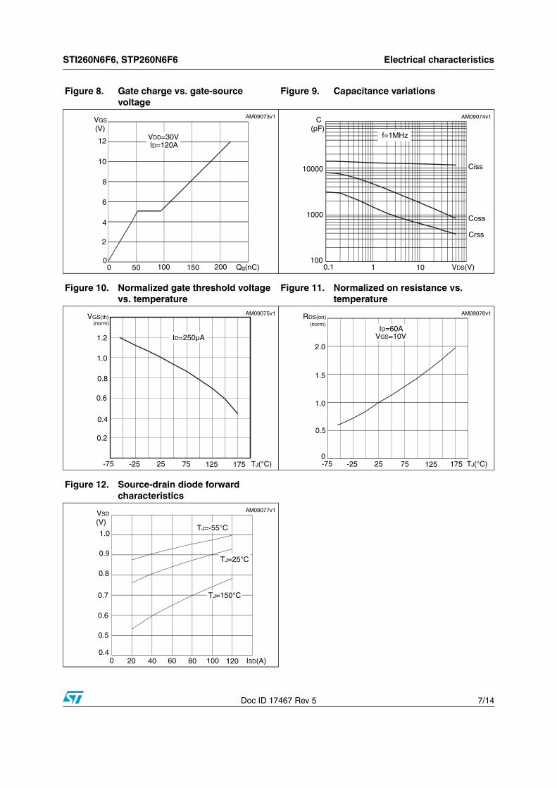
Figure 8. Gate charge vs. gate-source voltage
Figure 9. Capacitance variations
Figure 10. Normalized gate threshold voltage vs. temperature
Figure 11. Normalized on resistance vs. temperature
Figure 12. Source-drain diode forward characteristics
VGS
6
4
2
00 50 Qg(nC)
(V)
200
8
100 150
10
VDD=30VID=120A12
AM09073v1 C
1000
1000.1 10 VDS(V)
(pF)
1
10000 Ciss
Coss
Crss
f=1MHz
AM09074v1
VGS(th)
0.8
0.6
0.4
0.2
-75 TJ(°C)
(norm)
-25
1.0
7525 125 175
ID=250µA1.2
AM09075v1 RDS(on)
2.0
1.5
1.0
0.5
-75 TJ(°C)
(norm)
-25 7525 125 1750
ID=60AVGS=10V
AM09076v1
VSD
0 40 ISD(A)
(V)
20 10060 800.4
0.5
0.6
0.7
0.8
0.9
1.0TJ=-55°C
TJ=150°C
TJ=25°C
120
AM09077v1
Test circuits STI260N6F6, STP260N6F6
8/14 Doc ID 17467 Rev 5
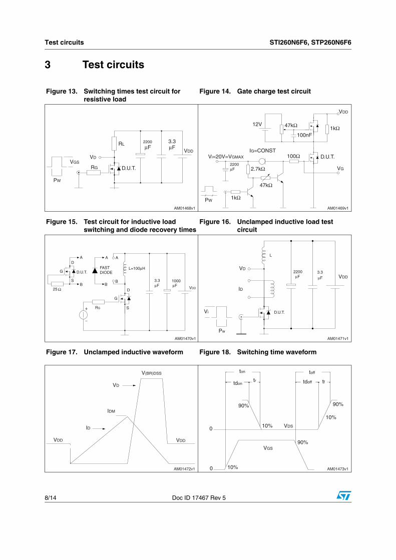
3 Test circuits
Figure 13. Switching times test circuit for resistive load
Figure 14. Gate charge test circuit
Figure 15. Test circuit for inductive load switching and diode recovery times
Figure 16. Unclamped inductive load test circuit
Figure 17. Unclamped inductive waveform Figure 18. Switching time waveform
AM01468v1
VGS
PW
VD
RG
RL
D.U.T.
2200
μF3.3μF
VDD
AM01469v1
VDD
47kΩ 1kΩ
47kΩ
2.7kΩ
1kΩ
12V
Vi=20V=VGMAX
2200μF
PW
IG=CONST100Ω
100nF
D.U.T.
VG
AM01470v1
AD
D.U.T.
SB
G
25 Ω
A A
BB
RG
G
FASTDIODE
D
S
L=100μH
μF3.3 1000
μF VDD
AM01471v1
Vi
Pw
VD
ID
D.U.T.
L
2200μF
3.3μF VDD
AM01472v1
V(BR)DSS
VDDVDD
VD
IDM
ID
AM01473v1
VDS
ton
tdon tdoff
toff
tftr
90%
10%
10%
0
0
90%
90%
10%
VGS
STI260N6F6, STP260N6F6 Package mechanical data
Doc ID 17467 Rev 5 9/14
4 Package mechanical data
In order to meet environmental requirements, ST offers these devices in different grades of ECOPACK® packages, depending on their level of environmental compliance. ECOPACK® specifications, grade definitions and product status are available at: www.st.com. ECOPACK is an ST trademark.
Package mechanical data STI260N6F6, STP260N6F6
10/14 Doc ID 17467 Rev 5
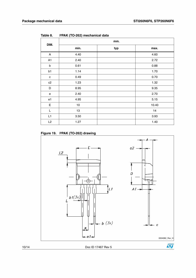
Figure 19. I²PAK (TO-262) drawing
Table 8. I²PAK (TO-262) mechanical data
DIM.mm.
min. typ max.
A 4.40 4.60
A1 2.40 2.72
b 0.61 0.88
b1 1.14 1.70
c 0.49 0.70
c2 1.23 1.32
D 8.95 9.35
e 2.40 2.70
e1 4.95 5.15
E 10 10.40
L 13 14
L1 3.50 3.93
L2 1.27 1.40
0004982_Rev_H
STI260N6F6, STP260N6F6 Package mechanical data
Doc ID 17467 Rev 5 11/14
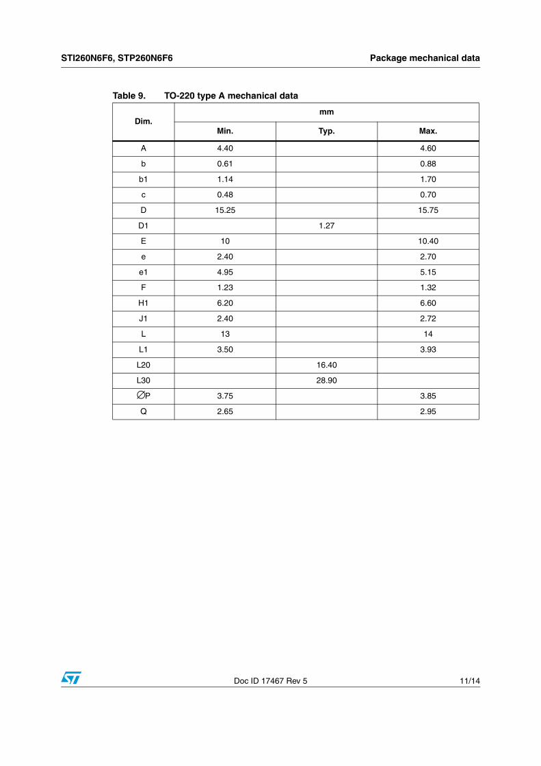
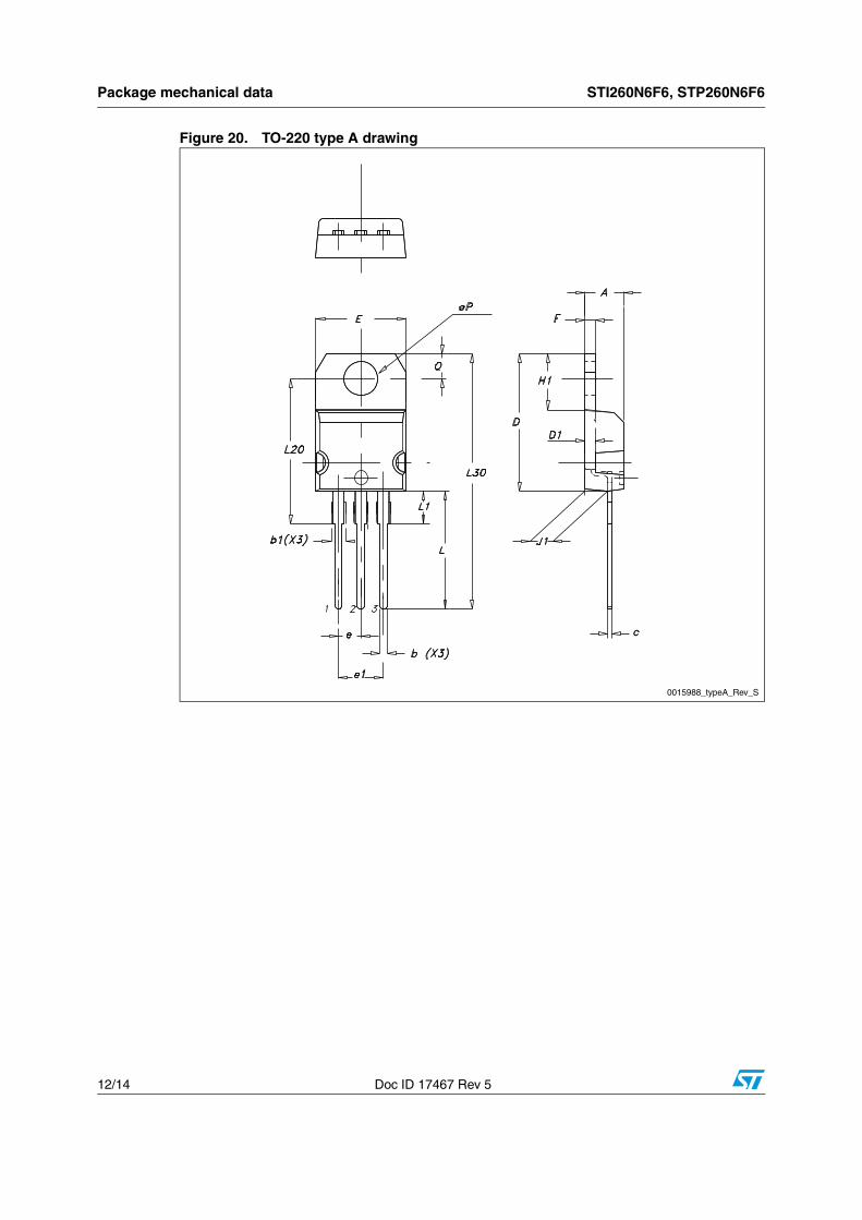
Table 9. TO-220 type A mechanical data
Dim.mm
Min. Typ. Max.
A 4.40 4.60
b 0.61 0.88
b1 1.14 1.70
c 0.48 0.70
D 15.25 15.75
D1 1.27
E 10 10.40
e 2.40 2.70
e1 4.95 5.15
F 1.23 1.32
H1 6.20 6.60
J1 2.40 2.72
L 13 14
L1 3.50 3.93
L20 16.40
L30 28.90
∅P 3.75 3.85
Q 2.65 2.95
Package mechanical data STI260N6F6, STP260N6F6
12/14 Doc ID 17467 Rev 5
Figure 20. TO-220 type A drawing
0015988_typeA_Rev_S
STI260N6F6, STP260N6F6 Revision history
Doc ID 17467 Rev 5 13/14
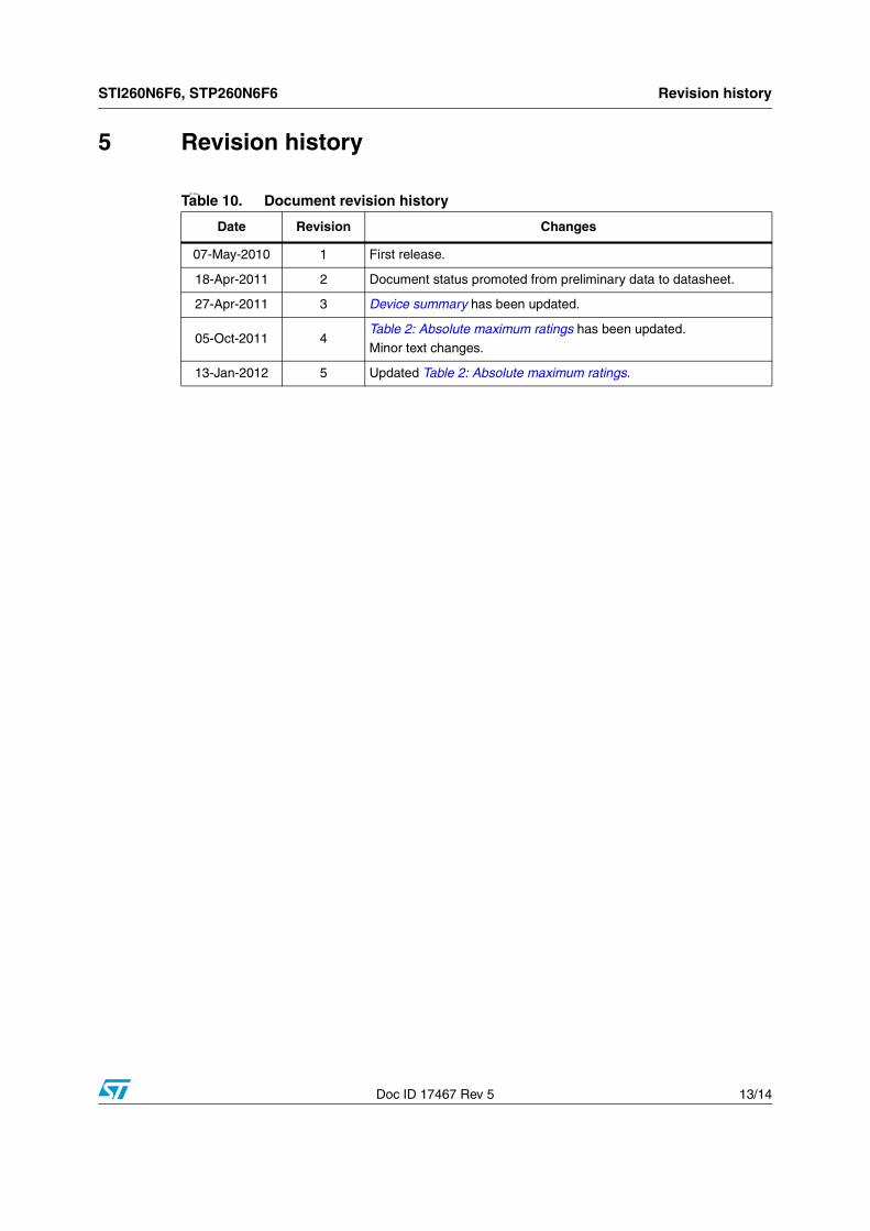
5 Revision history
07-Nov
Table 10. Document revision history
Date Revision Changes
07-May-2010 1 First release.
18-Apr-2011 2 Document status promoted from preliminary data to datasheet.
27-Apr-2011 3 Device summary has been updated.
05-Oct-2011 4Table 2: Absolute maximum ratings has been updated.Minor text changes.
13-Jan-2012 5 Updated Table 2: Absolute maximum ratings.
STI260N6F6, STP260N6F6
14/14 Doc ID 17467 Rev 5
Please Read Carefully:
Information in this document is provided solely in connection with ST products. STMicroelectronics NV and its subsidiaries (“ST”) reserve theright to make changes, corrections, modifications or improvements, to this document, and the products and services described herein at anytime, without notice.
All ST products are sold pursuant to ST’s terms and conditions of sale.
Purchasers are solely responsible for the choice, selection and use of the ST products and services described herein, and ST assumes noliability whatsoever relating to the choice, selection or use of the ST products and services described herein.
No license, express or implied, by estoppel or otherwise, to any intellectual property rights is granted under this document. If any part of thisdocument refers to any third party products or services it shall not be deemed a license grant by ST for the use of such third party productsor services, or any intellectual property contained therein or considered as a warranty covering the use in any manner whatsoever of suchthird party products or services or any intellectual property contained therein.
UNLESS OTHERWISE SET FORTH IN ST’S TERMS AND CONDITIONS OF SALE ST DISCLAIMS ANY EXPRESS OR IMPLIEDWARRANTY WITH RESPECT TO THE USE AND/OR SALE OF ST PRODUCTS INCLUDING WITHOUT LIMITATION IMPLIEDWARRANTIES OF MERCHANTABILITY, FITNESS FOR A PARTICULAR PURPOSE (AND THEIR EQUIVALENTS UNDER THE LAWSOF ANY JURISDICTION), OR INFRINGEMENT OF ANY PATENT, COPYRIGHT OR OTHER INTELLECTUAL PROPERTY RIGHT.
UNLESS EXPRESSLY APPROVED IN WRITING BY TWO AUTHORIZED ST REPRESENTATIVES, ST PRODUCTS ARE NOTRECOMMENDED, AUTHORIZED OR WARRANTED FOR USE IN MILITARY, AIR CRAFT, SPACE, LIFE SAVING, OR LIFE SUSTAININGAPPLICATIONS, NOR IN PRODUCTS OR SYSTEMS WHERE FAILURE OR MALFUNCTION MAY RESULT IN PERSONAL INJURY,DEATH, OR SEVERE PROPERTY OR ENVIRONMENTAL DAMAGE. ST PRODUCTS WHICH ARE NOT SPECIFIED AS "AUTOMOTIVEGRADE" MAY ONLY BE USED IN AUTOMOTIVE APPLICATIONS AT USER’S OWN RISK.
Resale of ST products with provisions different from the statements and/or technical features set forth in this document shall immediately voidany warranty granted by ST for the ST product or service described herein and shall not create or extend in any manner whatsoever, anyliability of ST.
ST and the ST logo are trademarks or registered trademarks of ST in various countries.
Information in this document supersedes and replaces all information previously supplied.
The ST logo is a registered trademark of STMicroelectronics. All other names are the property of their respective owners.
© 2012 STMicroelectronics - All rights reserved
STMicroelectronics group of companies
Australia - Belgium - Brazil - Canada - China - Czech Republic - Finland - France - Germany - Hong Kong - India - Israel - Italy - Japan - Malaysia - Malta - Morocco - Philippines - Singapore - Spain - Sweden - Switzerland - United Kingdom - United States of America
www.st.com


![δ B 10= [( B/ B /( B/ B ) – 1] x 1000 - tu-freiberg.de · Isotopengeochemie und Geochronologie . M. Tichomirowa . δ. 11. B • Fraktionierung bei Absorbtion von gelöstem . 10.](https://static.fdocument.org/doc/165x107/5d48a8ec88c993047d8bbf61/-b-10-b-b-b-b-1-x-1000-tu-isotopengeochemie-und-geochronologie.jpg)