N-channel 500 V, 0.23 , 20 A SuperMESH Power MOSFET … · isd ≤ 17 a, di/dt ≤ 200 a/µs, vds...
12
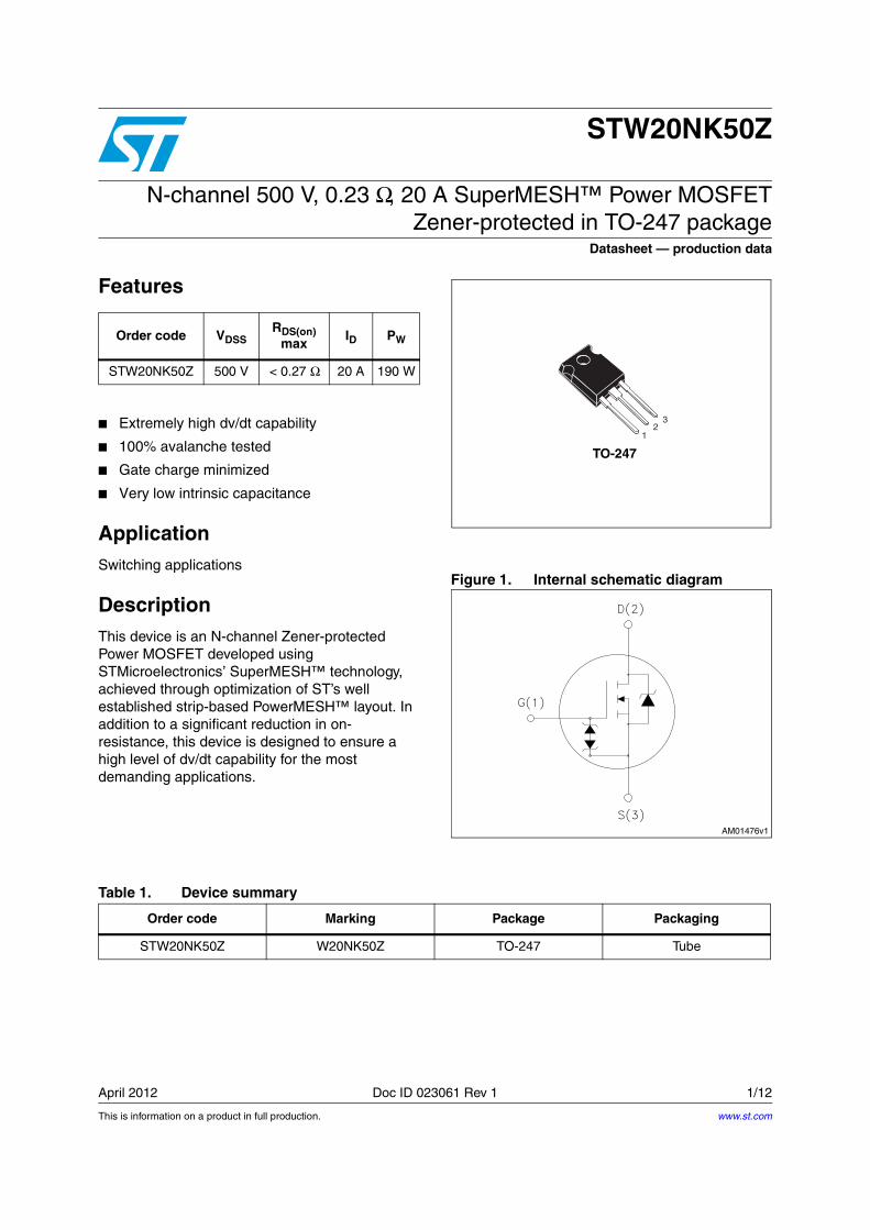
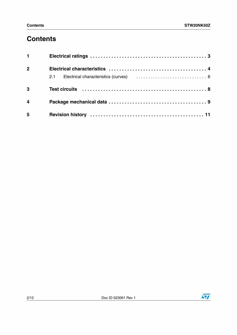
This is information on a product in full production. April 2012 Doc ID 023061 Rev 1 1/12 12 STW20NK50Z N-channel 500 V, 0.23 Ω , 20 A SuperMESH™ Power MOSFET Zener-protected in TO-247 package Datasheet — production data Features ■ Extremely high dv/dt capability ■ 100% avalanche tested ■ Gate charge minimized ■ Very low intrinsic capacitance Application Switching applications Description This device is an N-channel Zener-protected Power MOSFET developed using STMicroelectronics’ SuperMESH™ technology, achieved through optimization of ST’s well established strip-based PowerMESH™ layout. In addition to a significant reduction in on- resistance, this device is designed to ensure a high level of dv/dt capability for the most demanding applications. Figure 1. Internal schematic diagram Order code V DSS R DS(on) max I D P W STW20NK50Z 500 V < 0.27 Ω 20 A 190 W 1 2 3 TO-247 D(2) G(1) S(3) AM01476v1 Table 1. Device summary Order code Marking Package Packaging STW20NK50Z W20NK50Z TO-247 Tube www.st.com
Transcript of N-channel 500 V, 0.23 , 20 A SuperMESH Power MOSFET … · isd ≤ 17 a, di/dt ≤ 200 a/µs, vds...
This is information on a product in full production.
April 2012 Doc ID 023061 Rev 1 1/12
12
STW20NK50Z
N-channel 500 V, 0.23 Ω, 20 A SuperMESH™ Power MOSFETZener-protected in TO-247 package
Datasheet — production data
Features
■ Extremely high dv/dt capability
■ 100% avalanche tested
■ Gate charge minimized
■ Very low intrinsic capacitance
ApplicationSwitching applications
DescriptionThis device is an N-channel Zener-protected Power MOSFET developed using STMicroelectronics’ SuperMESH™ technology, achieved through optimization of ST’s well established strip-based PowerMESH™ layout. In addition to a significant reduction in on-resistance, this device is designed to ensure a high level of dv/dt capability for the most demanding applications.
Figure 1. Internal schematic diagram
Order code VDSSRDS(on)
maxID PW
STW20NK50Z 500 V < 0.27 Ω 20 A 190 W
12
3
TO-247
D(2)
G(1)
S(3)AM01476v1
Table 1. Device summary
Order code Marking Package Packaging
STW20NK50Z W20NK50Z TO-247 Tube
www.st.com
Contents STW20NK50Z
2/12 Doc ID 023061 Rev 1
Contents
1 Electrical ratings . . . . . . . . . . . . . . . . . . . . . . . . . . . . . . . . . . . . . . . . . . . . 3
2 Electrical characteristics . . . . . . . . . . . . . . . . . . . . . . . . . . . . . . . . . . . . . 4
2.1 Electrical characteristics (curves) . . . . . . . . . . . . . . . . . . . . . . . . . . . . . 6
3 Test circuits . . . . . . . . . . . . . . . . . . . . . . . . . . . . . . . . . . . . . . . . . . . . . . . 8
4 Package mechanical data . . . . . . . . . . . . . . . . . . . . . . . . . . . . . . . . . . . . . 9
5 Revision history . . . . . . . . . . . . . . . . . . . . . . . . . . . . . . . . . . . . . . . . . . . 11
STW20NK50Z Electrical ratings
Doc ID 023061 Rev 1 3/12
1 Electrical ratings
Table 2. Absolute maximum ratings
Symbol Parameter Value Unit
VDS Drain-source voltage 500 V
VGS Gate-source voltage ± 30 V
ID Drain current (continuous) at TC = 25 °C 20 A
ID Drain current (continuous) at TC = 100 °C 12.6 A
IDM (1)
1. Pulse width limited by safe operating area.
Drain current (pulsed) 68 A
PTOT Total dissipation at TC = 25 °C 190 W
Derating factor 1.52 W/°C
ESDGate-source human body model (R=1.5 kΩ, C=100 pF)
6 kV
dv/dt (2)
2. ISD ≤ 17 A, di/dt ≤ 200 A/µs, VDS peak ≤ V(BR)DSS, VDD ≤ V(BR)DSS, Tj ≤ TJMAX.
Peak diode recovery voltage slope 4.5 V/ns
Tstg Storage temperature -55 to 150 °C
Tj Max operating junction temperature 150 °C
Table 3. Thermal data
Symbol Parameter Value Unit
Rthj-case Thermal resistance junction-case max 0.66 °C/W
Rthj-amb Thermal resistance junction-ambient max 50 °C/W
Table 4. Avalanche characteristics
Symbol Parameter Value Unit
IARAvalanche current, repetitive or not-repetitive (pulse width limited by Tj Max)
17 A
EASSingle pulse avalanche energy(starting TJ=25 °C, ID=IAR, VDD=50 V)
850 mJ
Electrical characteristics STW20NK50Z
4/12 Doc ID 023061 Rev 1
2 Electrical characteristics
(TCASE = 25 °C unless otherwise specified)
Table 5. On/off states
Symbol Parameter Test conditions Min. Typ. Max. Unit
V(BR)DSSDrain-sourcebreakdown voltage
ID =1 mA, VGS = 0 500 V
IDSSZero gate voltage drain current (VGS = 0)
VDS = 500 VVDS = 500 V, TC = 125 °C
150
µAµA
IGSSGate-body leakagecurrent (VDS = 0)
VGS = ± 20 V ± 10 µA
VGS(th) Gate threshold voltage VDS = VGS, ID = 100 µA 3 3.75 4.5 V
RDS(on)Static drain-source
on-resistanceVGS = 10 V, ID = 8.5 A 0.23 0.27 Ω
Table 6. Dynamic
Symbol Parameter Test conditions Min. Typ. Max. Unit
Ciss
Coss
Crss
Input capacitanceOutput capacitanceReverse transfer capacitance
VDS = 25 V, f = 1 MHz, VGS = 0
-260032872
pFpFpF
Coss eq. (1)
1. Coss eq. is defined as a constant equivalent capacitance giving the same charging time as Coss when VDS increases from 0 to 80% VDSS.
Equivalent output capacitance
VDS =0, VDS = 0 to 640 V - 187 pF
td(on)
trtd(off)
tf
Turn-on delay time
Rise timeTurn-off delay timeFall time
VDD = 250 V, ID = 8.5 A, RG = 4.7 Ω, VGS = 10 V(see Figure 14)
-
28
207015
ns
nsnsns
Qg
Qgs
Qgd
Total gate chargeGate-source charge
Gate-drain charge
VDD = 400 V, ID = 17 A,VGS = 10 V
(see Figure 15)
-85
15.5
42
119 nCnC
nC
STW20NK50Z Electrical characteristics
Doc ID 023061 Rev 1 5/12
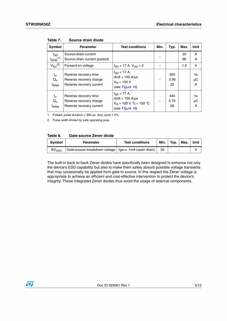
The built-in back-to-back Zener diodes have specifically been designed to enhance not only the device’s ESD capability, but also to make them safely absorb possible voltage transients that may occasionally be applied from gate to source. In this respect the Zener voltage is appropriate to achieve an efficient and cost-effective intervention to protect the device’s integrity. These integrated Zener diodes thus avoid the usage of external components.
Table 7. Source drain diode
Symbol Parameter Test conditions Min. Typ. Max. Unit
ISD
ISDM(1)
1. Pulsed: pulse duration = 300 µs, duty cycle 1.5%
Source-drain current
Source-drain current (pulsed)-
20
68
A
A
VSD(2)
2. Pulse width limited by safe operating area.
Forward on voltage ISD = 17 A, VGS = 0 - 1.6 V
trrQrr
IRRM
Reverse recovery timeReverse recovery charge
Reverse recovery current
ISD = 17 A, di/dt = 100 A/µs
VR = 100 V(see Figure 16)
-3553.90
22
nsµC
A
trrQrr
IRRM
Reverse recovery timeReverse recovery chargeReverse recovery current
ISD = 17 A, di/dt = 100 A/µsVR = 100 V, Tj = 150 °C
(see Figure 16)
-4405.7226
nsµCA
Table 8. Gate-source Zener diode
Symbol Parameter Test conditions Min. Typ. Max. Unit
BVGSO Gate-source breakdown voltage Igs=± 1mA (open drain) 30 - V
Electrical characteristics STW20NK50Z
6/12 Doc ID 023061 Rev 1
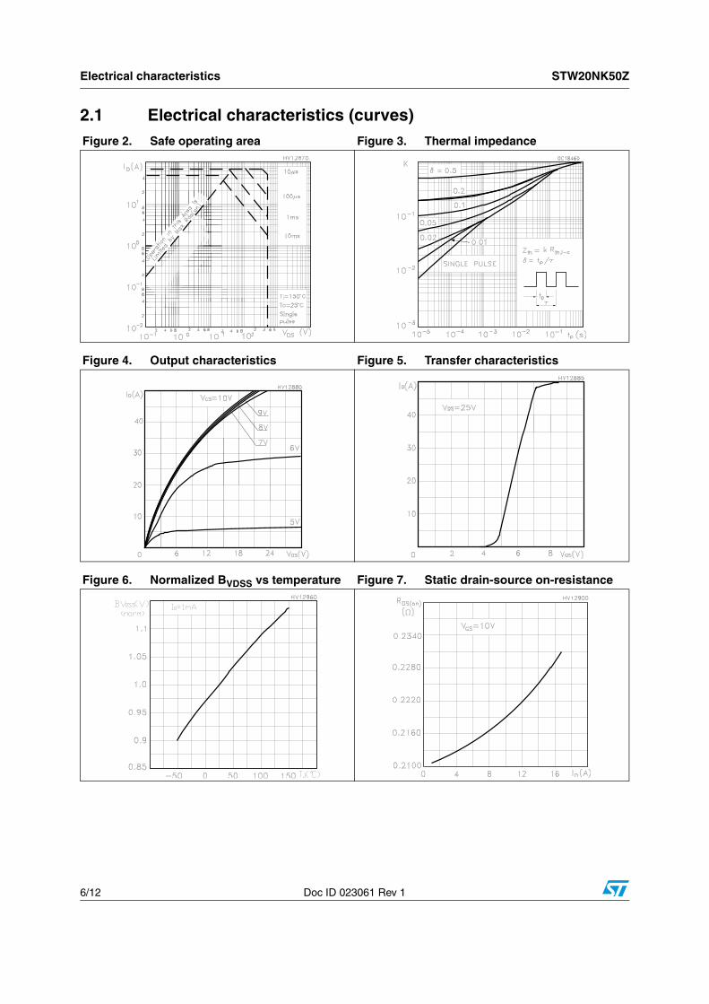
2.1 Electrical characteristics (curves) Figure 2. Safe operating area Figure 3. Thermal impedance
Figure 4. Output characteristics Figure 5. Transfer characteristics
Figure 6. Normalized BVDSS vs temperature Figure 7. Static drain-source on-resistance
STW20NK50Z Electrical characteristics
Doc ID 023061 Rev 1 7/12
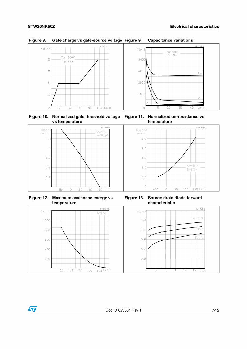
Figure 8. Gate charge vs gate-source voltage Figure 9. Capacitance variations
Figure 10. Normalized gate threshold voltage vs temperature
Figure 11. Normalized on-resistance vs temperature
Figure 12. Maximum avalanche energy vs temperature
Figure 13. Source-drain diode forward characteristic
Test circuits STW20NK50Z
8/12 Doc ID 023061 Rev 1
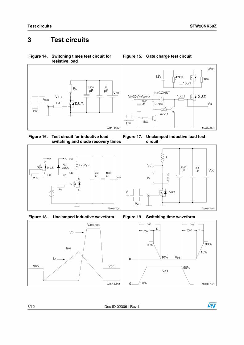
3 Test circuits
Figure 14. Switching times test circuit for resistive load
Figure 15. Gate charge test circuit
Figure 16. Test circuit for inductive load switching and diode recovery times
Figure 17. Unclamped inductive load test circuit
Figure 18. Unclamped inductive waveform Figure 19. Switching time waveform
AM01468v1
VGS
PW
VD
RG
RL
D.U.T.
2200
μF3.3μF
VDD
AM01469v1
VDD
47kΩ 1kΩ
47kΩ
2.7kΩ
1kΩ
12V
Vi=20V=VGMAX
2200μF
PW
IG=CONST100Ω
100nF
D.U.T.
VG
AM01470v1
AD
D.U.T.
SB
G
25 Ω
A A
BB
RG
G
FASTDIODE
D
S
L=100μH
μF3.3 1000
μF VDD
AM01471v1
Vi
Pw
VD
ID
D.U.T.
L
2200μF
3.3μF VDD
AM01472v1
V(BR)DSS
VDDVDD
VD
IDM
ID
AM01473v1
VDS
ton
tdon tdoff
toff
tftr
90%
10%
10%
0
0
90%
90%
10%
VGS
STW20NK50Z Package mechanical data
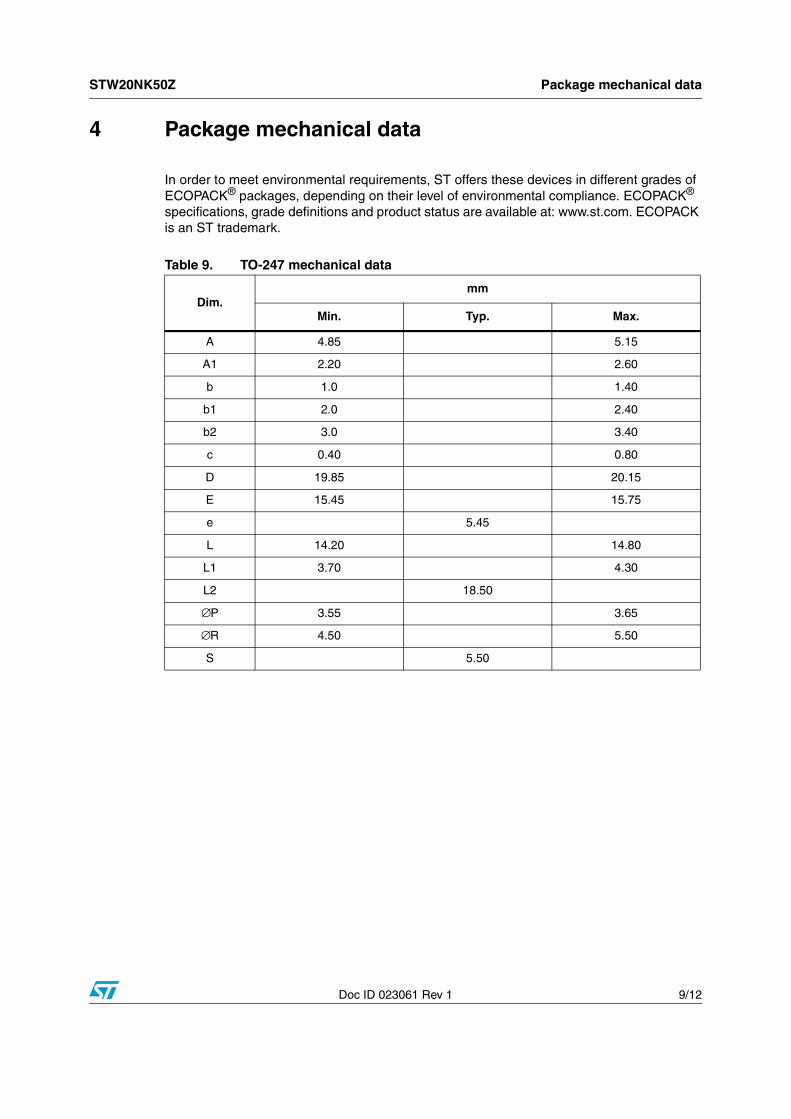
Doc ID 023061 Rev 1 9/12
4 Package mechanical data
In order to meet environmental requirements, ST offers these devices in different grades of ECOPACK® packages, depending on their level of environmental compliance. ECOPACK® specifications, grade definitions and product status are available at: www.st.com. ECOPACK is an ST trademark.
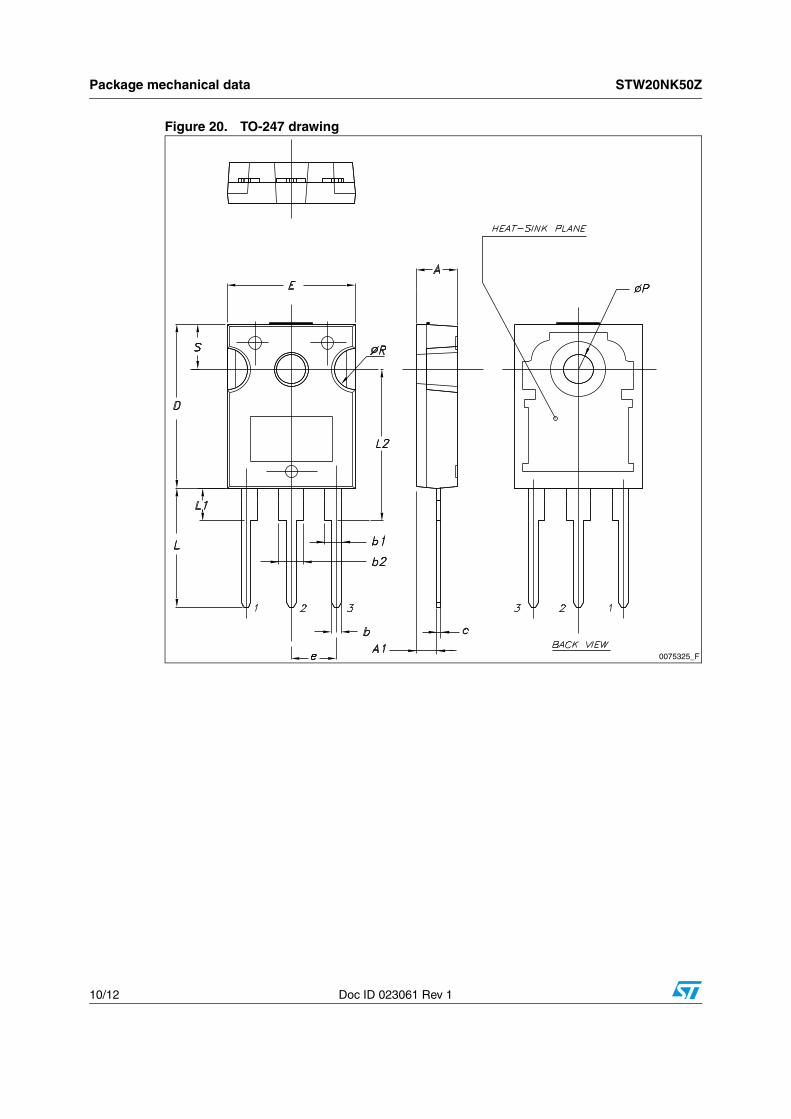
Table 9. TO-247 mechanical data
Dim.mm
Min. Typ. Max.
A 4.85 5.15
A1 2.20 2.60
b 1.0 1.40
b1 2.0 2.40
b2 3.0 3.40
c 0.40 0.80
D 19.85 20.15
E 15.45 15.75
e 5.45
L 14.20 14.80
L1 3.70 4.30
L2 18.50
∅P 3.55 3.65
∅R 4.50 5.50
S 5.50
Package mechanical data STW20NK50Z
10/12 Doc ID 023061 Rev 1
Figure 20. TO-247 drawing
0075325_F
STW20NK50Z Revision history
Doc ID 023061 Rev 1 11/12
5 Revision history
Table 10. Document revision history
Date Revision Changes
05-Apr-2012 1 First release.
STW20NK50Z
12/12 Doc ID 023061 Rev 1
Please Read Carefully:
Information in this document is provided solely in connection with ST products. STMicroelectronics NV and its subsidiaries (“ST”) reserve theright to make changes, corrections, modifications or improvements, to this document, and the products and services described herein at anytime, without notice.
All ST products are sold pursuant to ST’s terms and conditions of sale.
Purchasers are solely responsible for the choice, selection and use of the ST products and services described herein, and ST assumes noliability whatsoever relating to the choice, selection or use of the ST products and services described herein.
No license, express or implied, by estoppel or otherwise, to any intellectual property rights is granted under this document. If any part of thisdocument refers to any third party products or services it shall not be deemed a license grant by ST for the use of such third party productsor services, or any intellectual property contained therein or considered as a warranty covering the use in any manner whatsoever of suchthird party products or services or any intellectual property contained therein.
UNLESS OTHERWISE SET FORTH IN ST’S TERMS AND CONDITIONS OF SALE ST DISCLAIMS ANY EXPRESS OR IMPLIEDWARRANTY WITH RESPECT TO THE USE AND/OR SALE OF ST PRODUCTS INCLUDING WITHOUT LIMITATION IMPLIEDWARRANTIES OF MERCHANTABILITY, FITNESS FOR A PARTICULAR PURPOSE (AND THEIR EQUIVALENTS UNDER THE LAWSOF ANY JURISDICTION), OR INFRINGEMENT OF ANY PATENT, COPYRIGHT OR OTHER INTELLECTUAL PROPERTY RIGHT.
UNLESS EXPRESSLY APPROVED IN WRITING BY TWO AUTHORIZED ST REPRESENTATIVES, ST PRODUCTS ARE NOTRECOMMENDED, AUTHORIZED OR WARRANTED FOR USE IN MILITARY, AIR CRAFT, SPACE, LIFE SAVING, OR LIFE SUSTAININGAPPLICATIONS, NOR IN PRODUCTS OR SYSTEMS WHERE FAILURE OR MALFUNCTION MAY RESULT IN PERSONAL INJURY,DEATH, OR SEVERE PROPERTY OR ENVIRONMENTAL DAMAGE. ST PRODUCTS WHICH ARE NOT SPECIFIED AS "AUTOMOTIVEGRADE" MAY ONLY BE USED IN AUTOMOTIVE APPLICATIONS AT USER’S OWN RISK.
Resale of ST products with provisions different from the statements and/or technical features set forth in this document shall immediately voidany warranty granted by ST for the ST product or service described herein and shall not create or extend in any manner whatsoever, anyliability of ST.
ST and the ST logo are trademarks or registered trademarks of ST in various countries.
Information in this document supersedes and replaces all information previously supplied.
The ST logo is a registered trademark of STMicroelectronics. All other names are the property of their respective owners.
© 2012 STMicroelectronics - All rights reserved
STMicroelectronics group of companies
Australia - Belgium - Brazil - Canada - China - Czech Republic - Finland - France - Germany - Hong Kong - India - Israel - Italy - Japan - Malaysia - Malta - Morocco - Philippines - Singapore - Spain - Sweden - Switzerland - United Kingdom - United States of America
www.st.com