N-channel 30 V, 0.018 typ., 8 A, P-channel 30 V, …15 V, Tj =150 C Figure 28 N-15 ns P-45 ns Qrr...
18
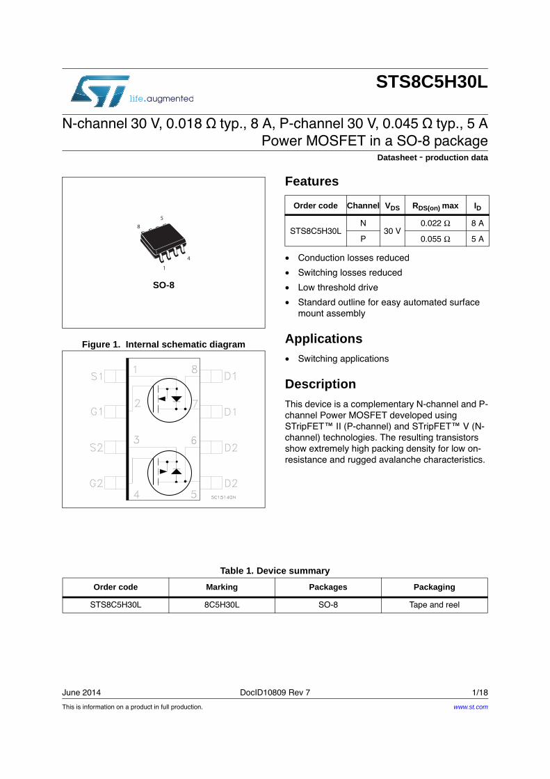
This is information on a product in full production. June 2014 DocID10809 Rev 7 1/18 STS8C5H30L N-channel 30 V, 0.018 Ω typ., 8 A, P-channel 30 V, 0.045 Ω typ., 5 A Power MOSFET in a SO-8 package Datasheet - production data Figure 1. Internal schematic diagram Features • Conduction losses reduced • Switching losses reduced • Low threshold drive • Standard outline for easy automated surface mount assembly Applications • Switching applications Description This device is a complementary N-channel and P- channel Power MOSFET developed using STripFET™ II (P-channel) and STripFET™ V (N- channel) technologies. The resulting transistors show extremely high packing density for low on- resistance and rugged avalanche characteristics. SO-8 5 8 4 1 Order code Channel V DS R DS(on) max I D STS8C5H30L N 30 V 0.022 Ω 8 A P 0.055 Ω 5 A Table 1. Device summary Order code Marking Packages Packaging STS8C5H30L 8C5H30L SO-8 Tape and reel www.st.com
Transcript of N-channel 30 V, 0.018 typ., 8 A, P-channel 30 V, …15 V, Tj =150 C Figure 28 N-15 ns P-45 ns Qrr...
This is information on a product in full production.
June 2014 DocID10809 Rev 7 1/18
STS8C5H30L
N-channel 30 V, 0.018 Ω typ., 8 A, P-channel 30 V, 0.045 Ω typ., 5 A
Power MOSFET in a SO-8 package
Datasheet - production data
Figure 1. Internal schematic diagram
Features
• Conduction losses reduced
• Switching losses reduced
• Low threshold drive
• Standard outline for easy automated surface
mount assembly
Applications• Switching applications
DescriptionThis device is a complementary N-channel and P-
channel Power MOSFET developed using
STripFET™ II (P-channel) and STripFET™ V (N-
channel) technologies. The resulting transistors
show extremely high packing density for low on-
resistance and rugged avalanche characteristics.
SO-8
58
4
1
Order code Channel VDS RDS(on) max ID
STS8C5H30L
N
30 V
0.022 Ω 8 A
P 0.055 Ω 5 A
Table 1. Device summary
Order code Marking Packages Packaging
STS8C5H30L 8C5H30L SO-8 Tape and reel
www.st.com
Contents STS8C5H30L
2/18 DocID10809 Rev 7
Contents
1 Electrical ratings . . . . . . . . . . . . . . . . . . . . . . . . . . . . . . . . . . . . . . . . . . . . 3
2 Electrical characteristics . . . . . . . . . . . . . . . . . . . . . . . . . . . . . . . . . . . . . 4
2.1 Electrical characteristics (curves) . . . . . . . . . . . . . . . . . . . . . . . . . . . . 7
3 Test circuits . . . . . . . . . . . . . . . . . . . . . . . . . . . . . . . . . . . . . . . . . . . . . 11
4 Package mechanical data . . . . . . . . . . . . . . . . . . . . . . . . . . . . . . . . . . . . 12
5 Packaging mechanical data . . . . . . . . . . . . . . . . . . . . . . . . . . . . . . . . . . 15
6 Revision history . . . . . . . . . . . . . . . . . . . . . . . . . . . . . . . . . . . . . . . . . . . 17
DocID10809 Rev 7 3/18
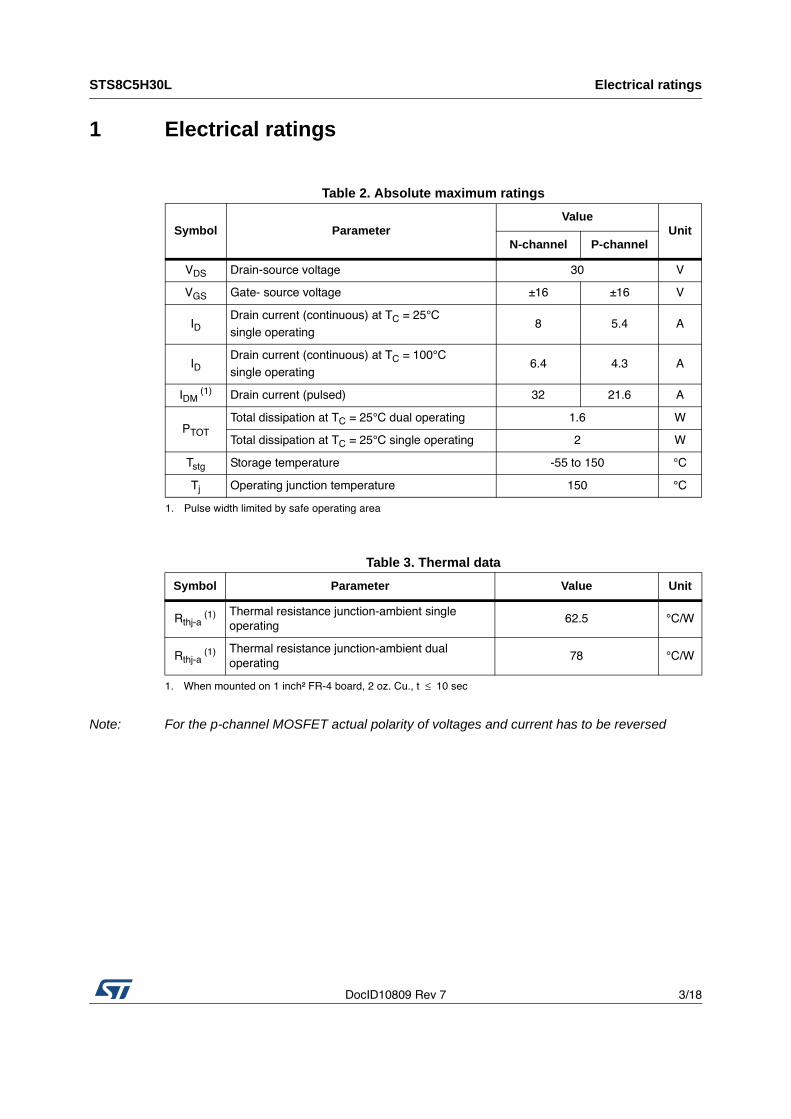
STS8C5H30L Electrical ratings
18
1 Electrical ratings
Note: For the p-channel MOSFET actual polarity of voltages and current has to be reversed
Table 2. Absolute maximum ratings
Symbol ParameterValue
UnitN-channel P-channel
VDS
Drain-source voltage 30 V
VGS
Gate- source voltage ±16 ±16 V
ID
Drain current (continuous) at TC
= 25°C
single operating
8 5.4 A
ID
Drain current (continuous) at TC
= 100°C
single operating
6.4 4.3 A
IDM
(1)
1. Pulse width limited by safe operating area
Drain current (pulsed) 32 21.6 A
PTOT
Total dissipation at TC
= 25°C dual operating 1.6 W
Total dissipation at TC
= 25°C single operating 2 W
Tstg
Storage temperature -55 to 150 °C
Tj
Operating junction temperature 150 °C
Table 3. Thermal data
Symbol Parameter Value Unit
Rthj-a
(1)
1. When mounted on 1 inch² FR-4 board, 2 oz. Cu., t ≤ 10 sec
Thermal resistance junction-ambient single
operating
62.5 °C/W
Rthj-a
(1)Thermal resistance junction-ambient dual
operating
78 °C/W
Electrical characteristics STS8C5H30L
4/18 DocID10809 Rev 7
2 Electrical characteristics
(TCASE
= 25 °C unless otherwise specified)
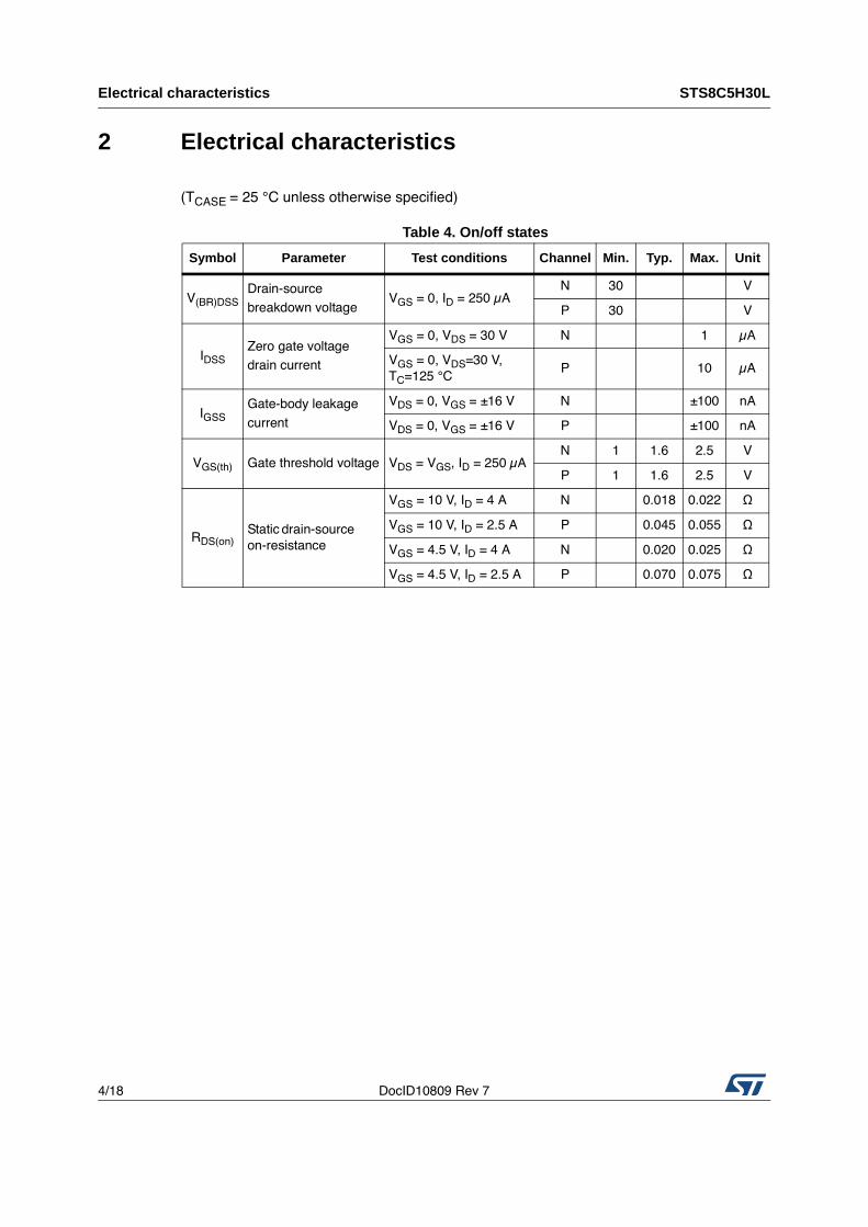
Table 4. On/off states
Symbol Parameter Test conditions Channel Min. Typ. Max. Unit
V(BR)DSS
Drain-source
breakdown voltage
VGS
= 0, ID
= 250 μA
N 30 V
P 30 V
IDSS
Zero gate voltage
drain current
VGS
= 0, VDS
= 30 V N 1 μA
VGS
= 0, VDS
=30 V,
TC
=125 °C
P 10 μA
IGSS
Gate-body leakage
current
VDS
= 0, VGS
= ±16 V N ±100 nA
VDS
= 0, VGS
= ±16 V P ±100 nA
VGS(th)
Gate threshold voltage VDS
= VGS
, ID
= 250 μA
N 1 1.6 2.5 V
P 1 1.6 2.5 V
RDS(on)
Static drain-source
on-resistance
VGS
= 10 V, ID
= 4 A N 0.018 0.022 Ω
VGS
= 10 V, ID
= 2.5 A P 0.045 0.055 Ω
VGS
= 4.5 V, ID
= 4 A N 0.020 0.025 Ω
VGS
= 4.5 V, ID
= 2.5 A P 0.070 0.075 Ω
DocID10809 Rev 7 5/18
STS8C5H30L Electrical characteristics
18
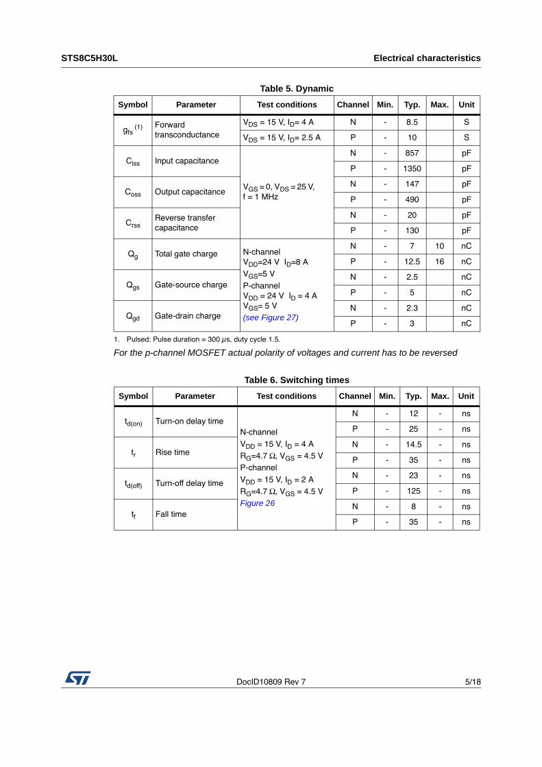
Table 5. Dynamic
Symbol Parameter Test conditions Channel Min. Typ. Max. Unit
gfs
(1)
1. Pulsed: Pulse duration = 300 μs, duty cycle 1.5.
For the p-channel MOSFET actual polarity of voltages and current has to be reversed
Forward
transconductance
VDS
= 15 V, ID
= 4 A N - 8.5 S
VDS
= 15 V, ID
= 2.5 A P - 10 S
Ciss
Input capacitance
VGS
= 0, VDS
= 25 V,
f = 1 MHz
N - 857 pF
P - 1350 pF
Coss
Output capacitance
N - 147 pF
P - 490 pF
Crss
Reverse transfer
capacitance
N - 20 pF
P - 130 pF
Qg
Total gate charge N-channel
VDD
=24 V ID
=8 A
VGS
=5 V
P-channel
VDD
= 24 V ID
= 4 A
VGS
= 5 V
(see Figure 27)
N - 7 10 nC
P - 12.5 16 nC
Qgs
Gate-source charge
N - 2.5 nC
P - 5 nC
Qgd
Gate-drain charge
N - 2.3 nC
P - 3 nC
Table 6. Switching times
Symbol Parameter Test conditions Channel Min. Typ. Max. Unit
td(on)
Turn-on delay time
N-channel
VDD
= 15 V, ID
= 4 A
RG
=4.7 Ω, VGS
= 4.5 V
P-channel
VDD
= 15 V, ID
= 2 A
RG
=4.7 Ω, VGS
= 4.5 V
Figure 26
N - 12 - ns
P - 25 - ns
tr
Rise time
N - 14.5 - ns
P - 35 - ns
td(off)
Turn-off delay time
N - 23 - ns
P - 125 - ns
tf
Fall time
N - 8 - ns
P - 35 - ns
Electrical characteristics STS8C5H30L
6/18 DocID10809 Rev 7
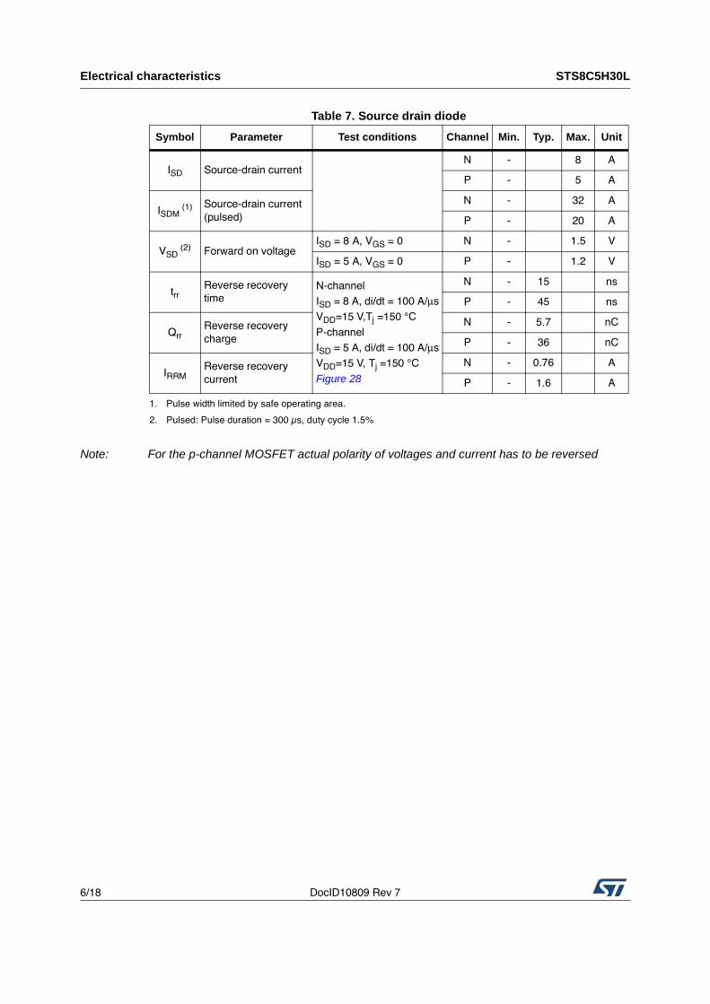
Note: For the p-channel MOSFET actual polarity of voltages and current has to be reversed
Table 7. Source drain diode
Symbol Parameter Test conditions Channel Min. Typ. Max. Unit
ISD
Source-drain current
N - 8 A
P - 5 A
ISDM
(1)
1. Pulse width limited by safe operating area.
Source-drain current
(pulsed)
N - 32 A
P - 20 A
VSD
(2)
2. Pulsed: Pulse duration = 300 μs, duty cycle 1.5%
Forward on voltage
ISD
= 8 A, VGS
= 0 N - 1.5 V
ISD
= 5 A, VGS
= 0 P - 1.2 V
trr
Reverse recovery
time
N-channel
ISD
= 8 A, di/dt = 100 A/μs
VDD
=15 V,Tj =150 °C
P-channel
ISD
= 5 A, di/dt = 100 A/μs
VDD
=15 V, Tj =150 °C
Figure 28
N - 15 ns
P - 45 ns
Qrr
Reverse recovery
charge
N - 5.7 nC
P - 36 nC
IRRM
Reverse recovery
current
N - 0.76 A
P - 1.6 A
DocID10809 Rev 7 7/18
STS8C5H30L Electrical characteristics
18
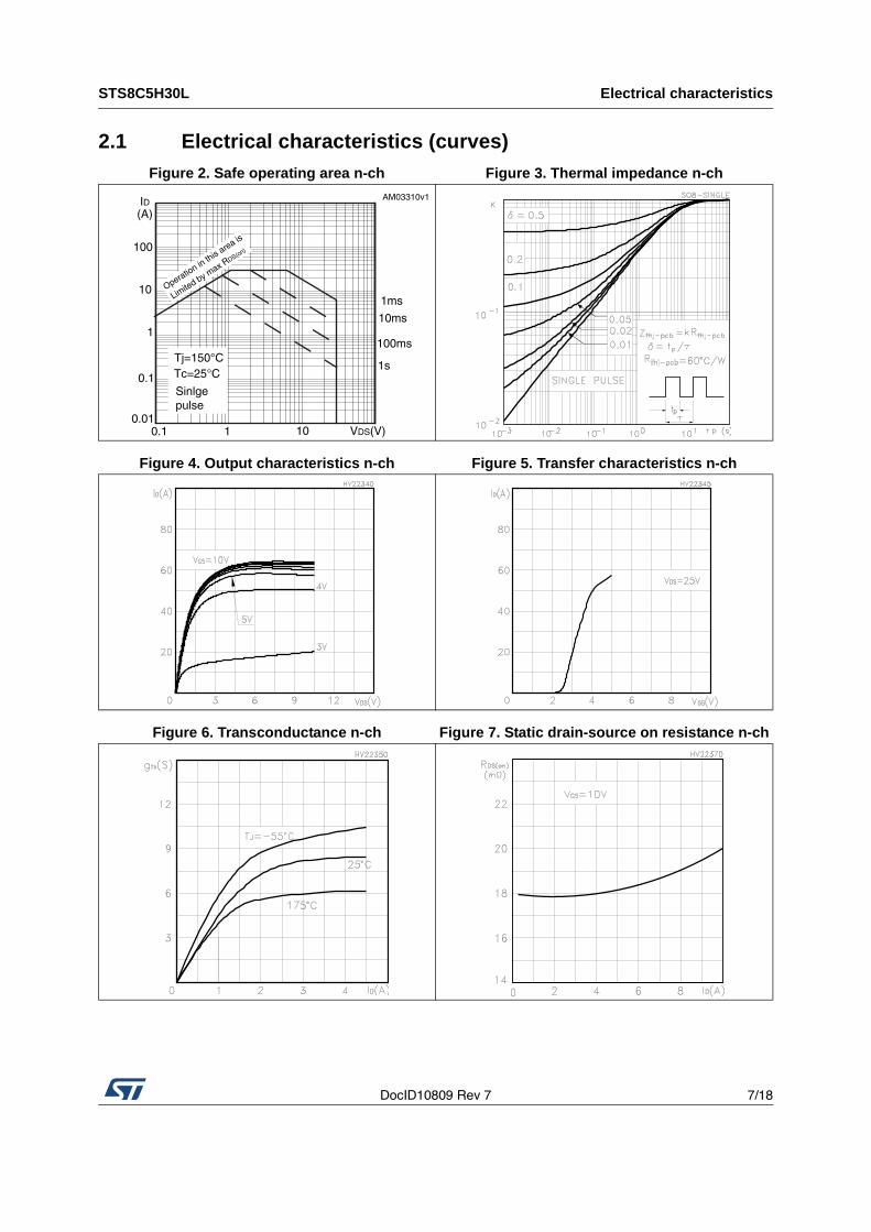
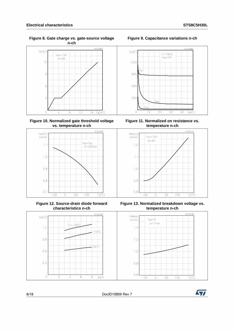
2.1 Electrical characteristics (curves) Figure 2. Safe operating area n-ch Figure 3. Thermal impedance n-ch
Figure 4. Output characteristics n-ch Figure 5. Transfer characteristics n-ch
Figure 6. Transconductance n-ch Figure 7. Static drain-source on resistance n-ch
ID
1
0.1
0.010.1 1 VDS(V)10
(A)
Operation in
this area is
Limite
d by max RDS(on)
1ms
10ms
100ms
1sTj=150°CTc=25°C
Sinlgepulse
10
100
AM03310v1
Electrical characteristics STS8C5H30L
8/18 DocID10809 Rev 7
Figure 8. Gate charge vs. gate-source voltage n-ch
Figure 9. Capacitance variations n-ch
Figure 10. Normalized gate threshold voltage vs. temperature n-ch
Figure 11. Normalized on resistance vs. temperature n-ch
Figure 12. Source-drain diode forward characteristics n-ch
Figure 13. Normalized breakdown voltage vs. temperature n-ch
DocID10809 Rev 7 9/18
STS8C5H30L Electrical characteristics
18
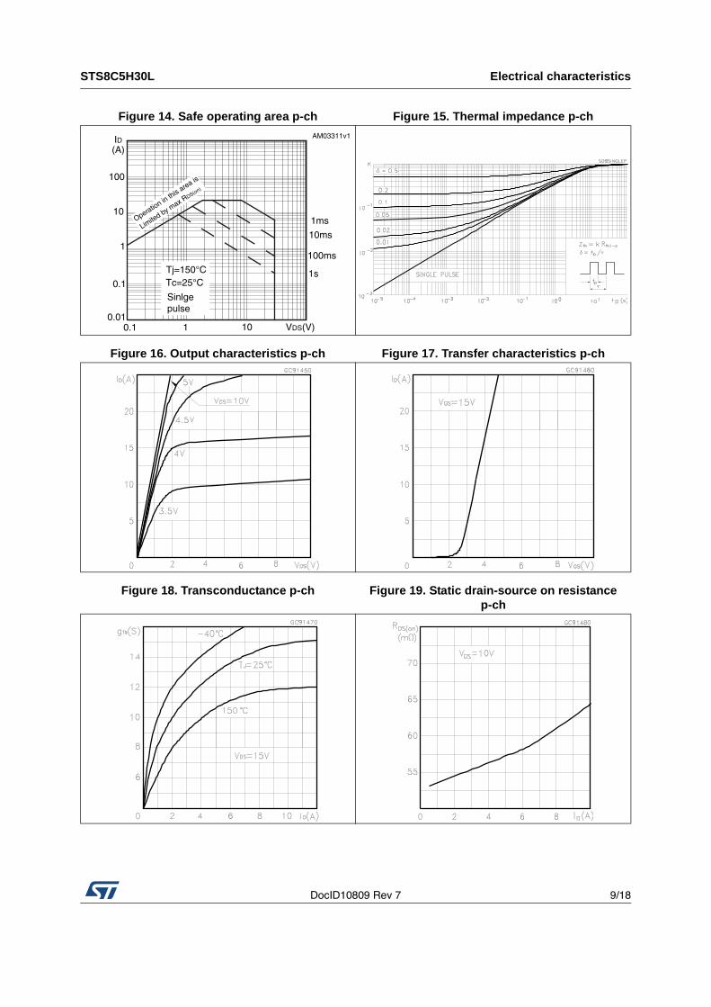
Figure 14. Safe operating area p-ch Figure 15. Thermal impedance p-ch
Figure 16. Output characteristics p-ch Figure 17. Transfer characteristics p-ch
Figure 18. Transconductance p-ch Figure 19. Static drain-source on resistancep-ch
ID
1
0.1
0.010.1 1 VDS(V)10
(A)
Operation in
this area is
Limite
d by max RDS(on)
1ms
10ms
100ms
1sTj=150°CTc=25°C
Sinlgepulse
10
100
AM03311v1
Electrical characteristics STS8C5H30L
10/18 DocID10809 Rev 7
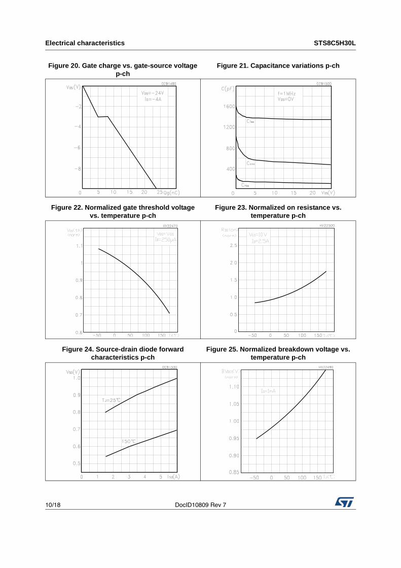
Figure 20. Gate charge vs. gate-source voltage p-ch
Figure 21. Capacitance variations p-ch
Figure 22. Normalized gate threshold voltage vs. temperature p-ch
Figure 23. Normalized on resistance vs. temperature p-ch
Figure 24. Source-drain diode forward characteristics p-ch
Figure 25. Normalized breakdown voltage vs. temperature p-ch
DocID10809 Rev 7 11/18
STS8C5H30L Test circuits
18
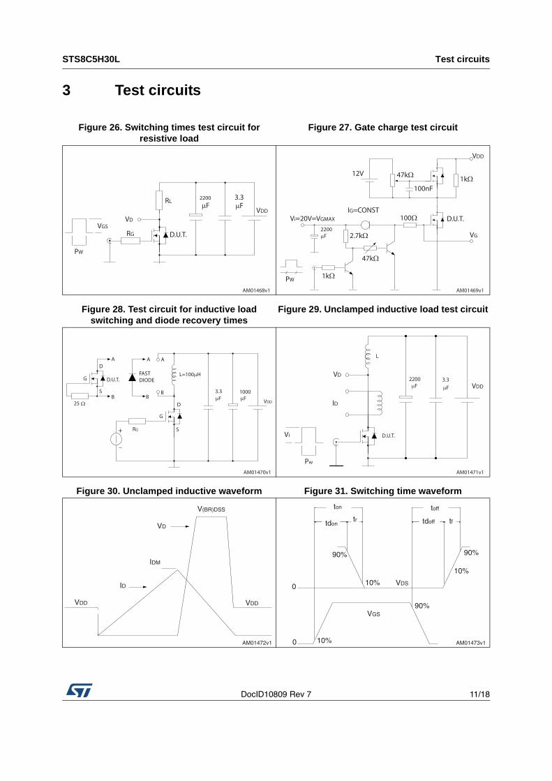
3 Test circuits
Figure 26. Switching times test circuit for resistive load
Figure 27. Gate charge test circuit
Figure 28. Test circuit for inductive load switching and diode recovery times
Figure 29. Unclamped inductive load test circuit
Figure 30. Unclamped inductive waveform Figure 31. Switching time waveform
AM01468v1
VGS
PW
VD
RG
RL
D.U.T.
2200
μF3.3μF
VDD
AM01469v1
VDD
47kΩ 1kΩ
47kΩ
2.7kΩ
1kΩ
12V
Vi=20V=VGMAX
2200μF
PW
IG=CONST100Ω
100nF
D.U.T.
VG
AM01470v1
AD
D.U.T.
SB
G
25 Ω
A A
BB
RG
G
FASTDIODE
D
S
L=100μH
μF3.3 1000
μF VDD
AM01471v1
Vi
Pw
VD
ID
D.U.T.
L
2200μF
3.3μF VDD
AM01472v1
V(BR)DSS
VDDVDD
VD
IDM
ID
AM01473v1
VDS
ton
tdon tdoff
toff
tftr
90%
10%
10%
0
0
90%
90%
10%
VGS
Package mechanical data STS8C5H30L
12/18 DocID10809 Rev 7
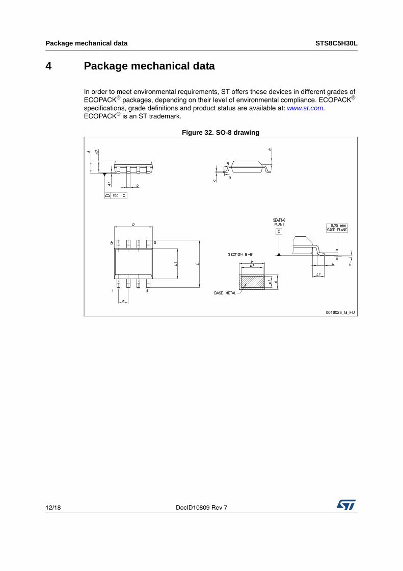
4 Package mechanical data
In order to meet environmental requirements, ST offers these devices in different grades of
ECOPACK®
packages, depending on their level of environmental compliance. ECOPACK®
specifications, grade definitions and product status are available at: www.st.com.
ECOPACK®
is an ST trademark.
Figure 32. SO-8 drawing
0016023_G_FU
DocID10809 Rev 7 13/18
STS8C5H30L Package mechanical data
18
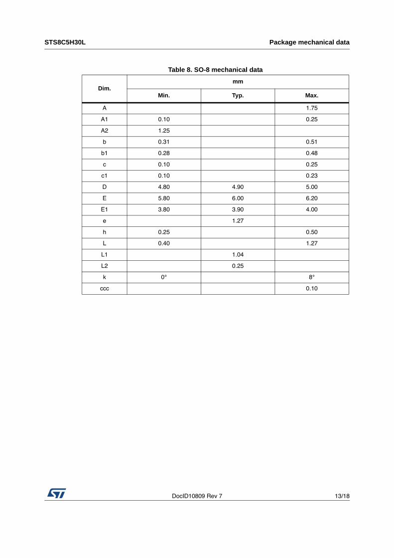
Table 8. SO-8 mechanical data
Dim.mm
Min. Typ. Max.
A 1.75
A1 0.10 0.25
A2 1.25
b 0.31 0.51
b1 0.28 0.48
c 0.10 0.25
c1 0.10 0.23
D 4.80 4.90 5.00
E 5.80 6.00 6.20
E1 3.80 3.90 4.00
e 1.27
h 0.25 0.50
L 0.40 1.27
L1 1.04
L2 0.25
k 0° 8°
ccc 0.10
Package mechanical data STS8C5H30L
14/18 DocID10809 Rev 7
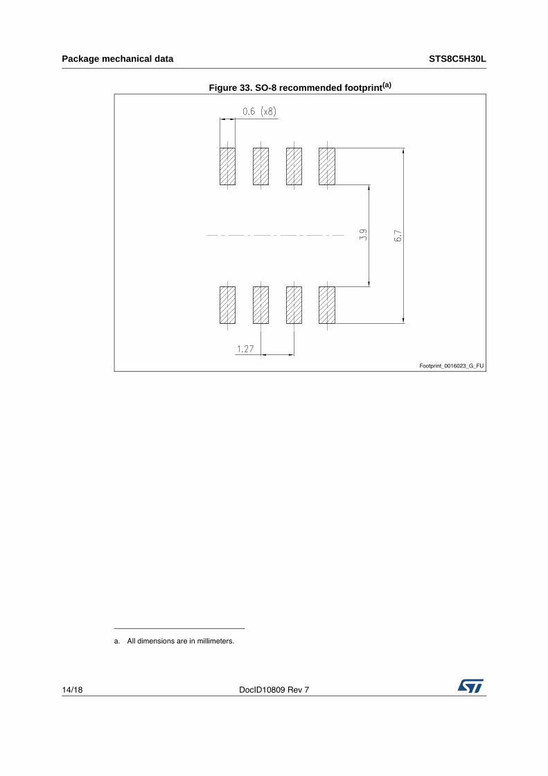
Figure 33. SO-8 recommended footprint(a)
a. All dimensions are in millimeters.
Footprint_0016023_G_FU
DocID10809 Rev 7 15/18
STS8C5H30L Packaging mechanical data
18
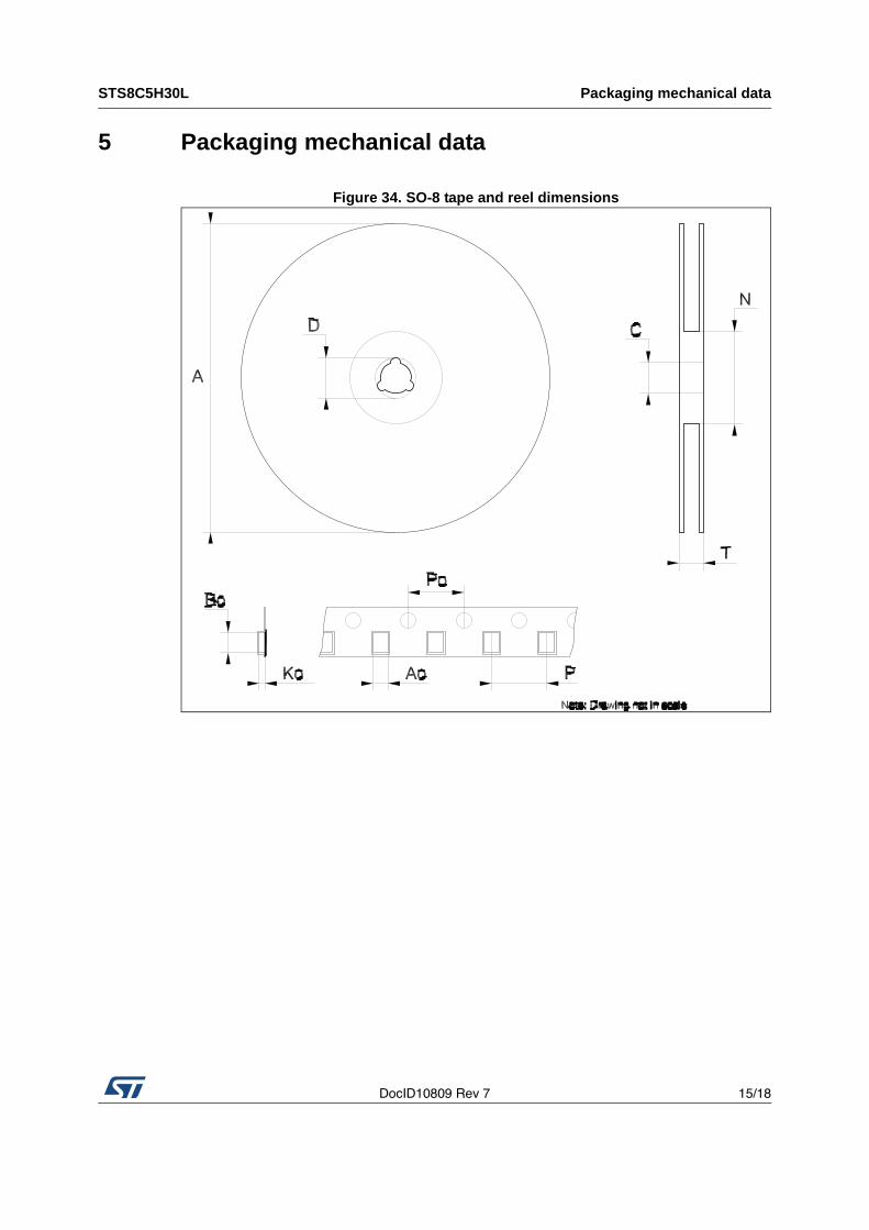
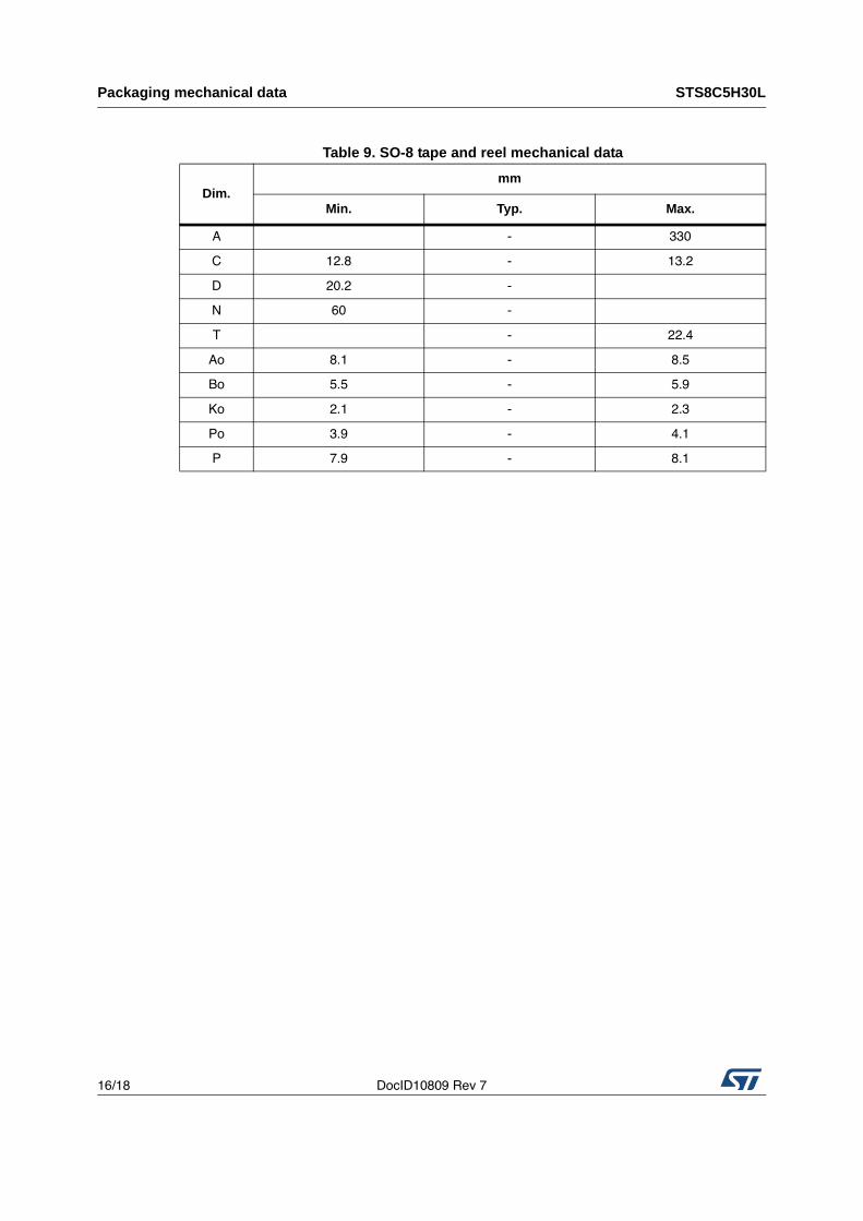
5 Packaging mechanical data
Figure 34. SO-8 tape and reel dimensions
Packaging mechanical data STS8C5H30L
16/18 DocID10809 Rev 7
Table 9. SO-8 tape and reel mechanical data
Dim.mm
Min. Typ. Max.
A - 330
C 12.8 - 13.2
D 20.2 -
N 60 -
T - 22.4
Ao 8.1 - 8.5
Bo 5.5 - 5.9
Ko 2.1 - 2.3
Po 3.9 - 4.1
P 7.9 - 8.1
DocID10809 Rev 7 17/18
STS8C5H30L Revision history
18
6 Revision history
Table 10. Revision history
Date Revision Changes
17-Sep-2004 1 First revision.
31-Oct-2006 2 The document has been reformatted.
30-Jan-2007 3 typo mistake on Table 2.
23-Jul-2007 4 Figure 14 has been updated.
23-Feb-2009 5 Figure 2, Figure 3, Figure 14 and Figure 15 have been changed.
10-Jun-2010 6 Updated VGS(th)
in Table 4: On/off states.
13-Jun-2014 7
– Modified: title
– Modified: Description
– Modified: marking in Table 1– Updated: Section 4: Package mechanical data– Minor text changes
STS8C5H30L
18/18 DocID10809 Rev 7
Please Read Carefully:
Information in this document is provided solely in connection with ST products. STMicroelectronics NV and its subsidiaries (“ST”) reserve the
right to make changes, corrections, modifications or improvements, to this document, and the products and services described herein at any
time, without notice.
All ST products are sold pursuant to ST’s terms and conditions of sale.
Purchasers are solely responsible for the choice, selection and use of the ST products and services described herein, and ST assumes no
liability whatsoever relating to the choice, selection or use of the ST products and services described herein.
No license, express or implied, by estoppel or otherwise, to any intellectual property rights is granted under this document. If any part of this
document refers to any third party products or services it shall not be deemed a license grant by ST for the use of such third party products
or services, or any intellectual property contained therein or considered as a warranty covering the use in any manner whatsoever of such
third party products or services or any intellectual property contained therein.
UNLESS OTHERWISE SET FORTH IN ST’S TERMS AND CONDITIONS OF SALE ST DISCLAIMS ANY EXPRESS OR IMPLIEDWARRANTY WITH RESPECT TO THE USE AND/OR SALE OF ST PRODUCTS INCLUDING WITHOUT LIMITATION IMPLIEDWARRANTIES OF MERCHANTABILITY, FITNESS FOR A PARTICULAR PURPOSE (AND THEIR EQUIVALENTS UNDER THE LAWSOF ANY JURISDICTION), OR INFRINGEMENT OF ANY PATENT, COPYRIGHT OR OTHER INTELLECTUAL PROPERTY RIGHT.
ST PRODUCTS ARE NOT DESIGNED OR AUTHORIZED FOR USE IN: (A) SAFETY CRITICAL APPLICATIONS SUCH AS LIFESUPPORTING, ACTIVE IMPLANTED DEVICES OR SYSTEMS WITH PRODUCT FUNCTIONAL SAFETY REQUIREMENTS; (B)AERONAUTIC APPLICATIONS; (C) AUTOMOTIVE APPLICATIONS OR ENVIRONMENTS, AND/OR (D) AEROSPACE APPLICATIONSOR ENVIRONMENTS. WHERE ST PRODUCTS ARE NOT DESIGNED FOR SUCH USE, THE PURCHASER SHALL USE PRODUCTS ATPURCHASER’S SOLE RISK, EVEN IF ST HAS BEEN INFORMED IN WRITING OF SUCH USAGE, UNLESS A PRODUCT ISEXPRESSLY DESIGNATED BY ST AS BEING INTENDED FOR “AUTOMOTIVE, AUTOMOTIVE SAFETY OR MEDICAL” INDUSTRYDOMAINS ACCORDING TO ST PRODUCT DESIGN SPECIFICATIONS. PRODUCTS FORMALLY ESCC, QML OR JAN QUALIFIED AREDEEMED SUITABLE FOR USE IN AEROSPACE BY THE CORRESPONDING GOVERNMENTAL AGENCY.
Resale of ST products with provisions different from the statements and/or technical features set forth in this document shall immediately void
any warranty granted by ST for the ST product or service described herein and shall not create or extend in any manner whatsoever, any
liability of ST.
ST and the ST logo are trademarks or registered trademarks of ST in various countries.
Information in this document supersedes and replaces all information previously supplied.
The ST logo is a registered trademark of STMicroelectronics. All other names are the property of their respective owners.
© 2014 STMicroelectronics - All rights reserved
STMicroelectronics group of companies
Australia - Belgium - Brazil - Canada - China - Czech Republic - Finland - France - Germany - Hong Kong - India - Israel - Italy - Japan -
Malaysia - Malta - Morocco - Philippines - Singapore - Spain - Sweden - Switzerland - United Kingdom - United States of America
www.st.com


![with: r) . ofstad - staff.uni-mainz.de fileof rm s ˆτ n (k = X x ∈ Z d τ n (x) e ik · x k ∈ [− π] d. r p c, ˆτ n (0) is small. r p c, ˆτ n (0) s n d. r p = p c, iour](https://static.fdocument.org/doc/165x107/5d4bbf8688c993237a8b922d/with-r-ofstad-staffuni-mainzde-rm-s-n-k-x-x-z-d-n-x-e-ik.jpg)


![arXiv:2006.15439v1 [math.NT] 27 Jun 2020 · We write the prime factorization of G nas G n= Y p p p(G n) (1.2) where p(G n) = ord p(G(n)). Since G n is an integer, p(G n) 0 for all](https://static.fdocument.org/doc/165x107/5f3385174ef0945b3871855e/arxiv200615439v1-mathnt-27-jun-2020-we-write-the-prime-factorization-of-g-nas.jpg)