N-channel 100 V, 0.012 , 80 A, TO-220, D²PAK low gate ... · Test circuits STB80NF10, STP80NF10...
14
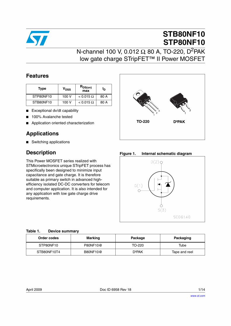
April 2009 Doc ID 6958 Rev 18 1/14 14 STB80NF10 STP80NF10 N-channel 100 V, 0.012 Ω , 80 A, TO-220, D 2 PAK low gate charge STripFET™ II Power MOSFET Features ■ Exceptional dv/dt capability ■ 100% Avalanche tested ■ Application oriented characterization Applications ■ Switching applications Description This Power MOSFET series realized with STMicroelectronics unique STripFET process has specifically been designed to minimize input capacitance and gate charge. It is therefore suitable as primary switch in advanced high- efficiency isolated DC-DC converters for telecom and computer application. It is also intended for any application with low gate charge drive requirements. Figure 1. Internal schematic diagram Type V DSS R DS(on) max I D STP80NF10 100 V < 0.015 Ω 80 A STB80NF10 100 V < 0.015 Ω 80 A 1 2 3 1 3 TO-220 D²PAK Table 1. Device summary Order codes Marking Package Packaging STP80NF10 P80NF10@ TO-220 Tube STB80NF10T4 B80NF10@ D²PAK Tape and reel www.st.com
Transcript of N-channel 100 V, 0.012 , 80 A, TO-220, D²PAK low gate ... · Test circuits STB80NF10, STP80NF10...
April 2009 Doc ID 6958 Rev 18 1/14
14
STB80NF10STP80NF10
N-channel 100 V, 0.012 Ω, 80 A, TO-220, D2PAKlow gate charge STripFET™ II Power MOSFET
Features
Exceptional dv/dt capability
100% Avalanche tested
Application oriented characterization
Applications Switching applications
DescriptionThis Power MOSFET series realized with STMicroelectronics unique STripFET process has specifically been designed to minimize input capacitance and gate charge. It is therefore suitable as primary switch in advanced high-efficiency isolated DC-DC converters for telecom and computer application. It is also intended for any application with low gate charge drive requirements.
Figure 1. Internal schematic diagram
Type VDSSRDS(on)
maxID
STP80NF10 100 V < 0.015 Ω 80 A
STB80NF10 100 V < 0.015 Ω 80 A
12
31
3
TO-220 D²PAK
Table 1. Device summary
Order codes Marking Package Packaging
STP80NF10 P80NF10@ TO-220 Tube
STB80NF10T4 B80NF10@ D²PAK Tape and reel
www.st.com
Contents STB80NF10, STP80NF10
2/14 Doc ID 6958 Rev 18
Contents
1 Electrical ratings . . . . . . . . . . . . . . . . . . . . . . . . . . . . . . . . . . . . . . . . . . . . 3
2 Electrical characteristics . . . . . . . . . . . . . . . . . . . . . . . . . . . . . . . . . . . . . 4
2.1 Electrical characteristics (curves) . . . . . . . . . . . . . . . . . . . . . . . . . . . . 5
3 Test circuit . . . . . . . . . . . . . . . . . . . . . . . . . . . . . . . . . . . . . . . . . . . . . . . . 8
4 Package mechanical data . . . . . . . . . . . . . . . . . . . . . . . . . . . . . . . . . . . . . 9
5 Packaging mechanical data . . . . . . . . . . . . . . . . . . . . . . . . . . . . . . . . . . 13
6 Revision history . . . . . . . . . . . . . . . . . . . . . . . . . . . . . . . . . . . . . . . . . . . 14
STB80NF10, STP80NF10 Electrical ratings
Doc ID 6958 Rev 18 3/14
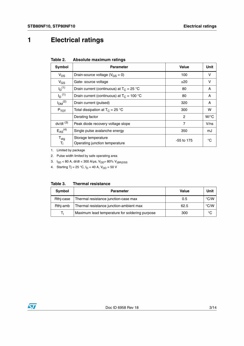
1 Electrical ratings
Table 2. Absolute maximum ratings
Symbol Parameter Value Unit
VDS Drain-source voltage (VGS = 0) 100 V
VGS Gate- source voltage ±20 V
ID(1)
1. Limited by package
Drain current (continuous) at TC = 25 °C 80 A
ID (1) Drain current (continuous) at TC = 100 °C 80 A
IDM(2)
2. Pulse width limited by safe operating area
Drain current (pulsed) 320 A
PTOT Total dissipation at TC = 25 °C 300 W
Derating factor 2 W/°C
dv/dt (3)
3. ISD < 80 A, di/dt < 300 A/µs, VDD= 80% V(BR)DSS
Peak diode recovery voltage slope 7 V/ns
EAS(4)
4. Starting Tj = 25 °C, ID = 40 A, VDD = 50 V
Single pulse avalanche energy 350 mJ
Tstg
Tj
Storage temperature
Operating junction temperature-55 to 175 °C
Table 3. Thermal resistance
Symbol Parameter Value Unit
Rthj-case Thermal resistance junction-case max 0.5 °C/W
Rthj-amb Thermal resistance junction-ambient max 62.5 °C/W
Tl Maximum lead temperature for soldering purpose 300 °C
Electrical characteristics STB80NF10, STP80NF10
4/14 Doc ID 6958 Rev 18
2 Electrical characteristics
(TCASE=25 °C unless otherwise specified)
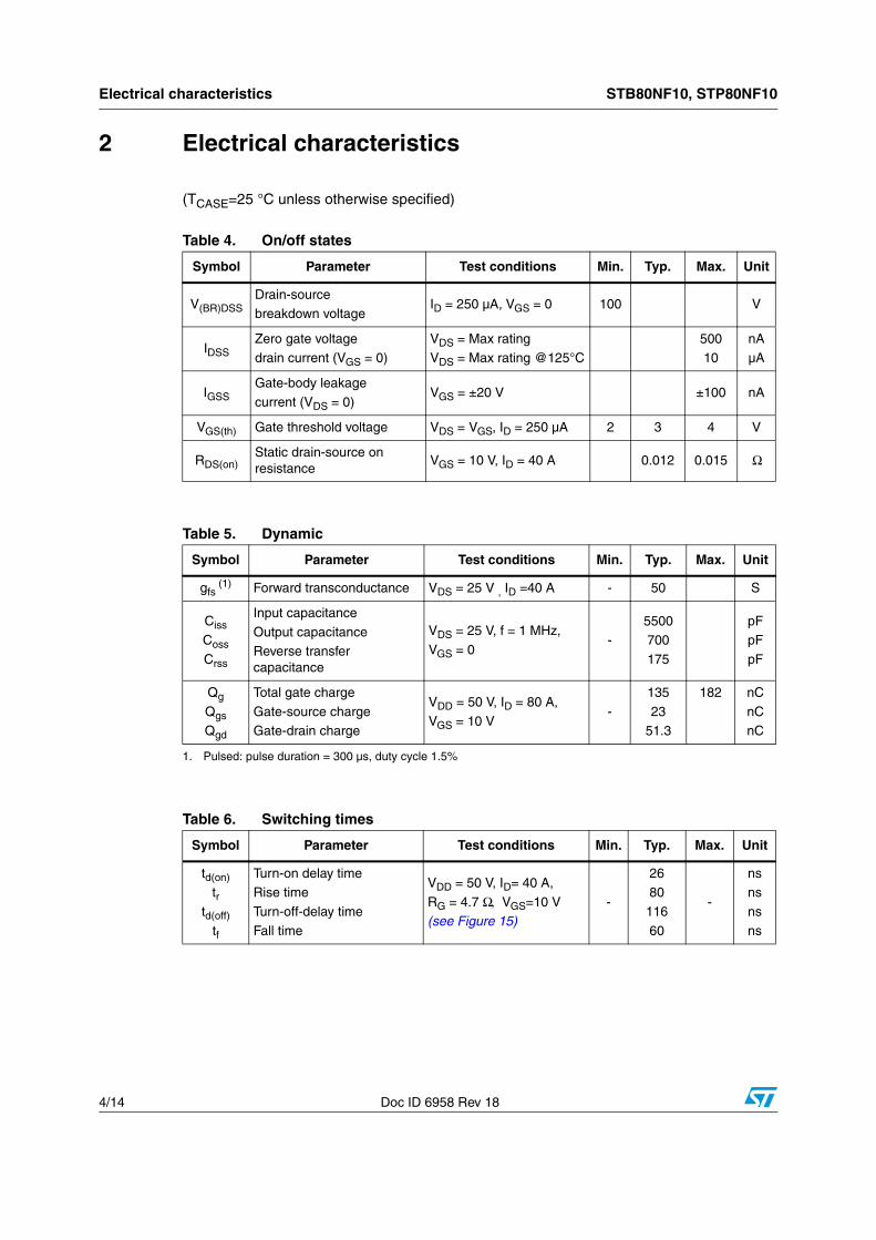
Table 4. On/off states
Symbol Parameter Test conditions Min. Typ. Max. Unit
V(BR)DSSDrain-source breakdown voltage
ID = 250 µA, VGS = 0 100 V
IDSSZero gate voltage drain current (VGS = 0)
VDS = Max ratingVDS = Max rating @125°C
50010
nAµA
IGSSGate-body leakagecurrent (VDS = 0)
VGS = ±20 V ±100 nA
VGS(th) Gate threshold voltage VDS = VGS, ID = 250 µA 2 3 4 V
RDS(on)Static drain-source on resistance
VGS = 10 V, ID = 40 A 0.012 0.015 Ω
Table 5. Dynamic
Symbol Parameter Test conditions Min. Typ. Max. Unit
gfs (1)
1. Pulsed: pulse duration = 300 µs, duty cycle 1.5%
Forward transconductance VDS = 25 V , ID =40 A - 50 S
Ciss
Coss
Crss
Input capacitance
Output capacitanceReverse transfer capacitance
VDS = 25 V, f = 1 MHz,
VGS = 0-
5500700
175
pFpF
pF
Qg
Qgs
Qgd
Total gate charge
Gate-source chargeGate-drain charge
VDD = 50 V, ID = 80 A,
VGS = 10 V-
135
2351.3
182 nC
nCnC
Table 6. Switching times
Symbol Parameter Test conditions Min. Typ. Max. Unit
td(on)
trtd(off)
tf
Turn-on delay timeRise time
Turn-off-delay time
Fall time
VDD = 50 V, ID= 40 A,
RG = 4.7 Ω, VGS=10 V(see Figure 15)
-
2680
116
60
-
nsns
ns
ns
STB80NF10, STP80NF10 Electrical characteristics
Doc ID 6958 Rev 18 5/14
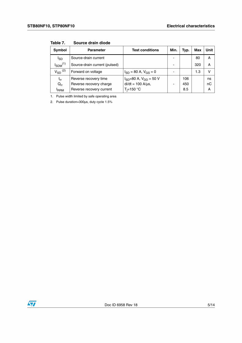
Table 7. Source drain diode
Symbol Parameter Test conditions Min. Typ. Max Unit
ISD Source-drain current - 80 A
ISDM(1)
1. Pulse width limited by safe operating area
Source-drain current (pulsed) - 320 A
VSD (2)
2. Pulse duration=300µs, duty cycle 1.5%
Forward on voltage ISD = 80 A, VGS = 0 - 1.3 V
trrQrr
IRRM
Reverse recovery time
Reverse recovery chargeReverse recovery current
ISD=80 A, VDD = 50 V
di/dt = 100 A/µs,Tj=150 °C
-
106
4508.5
ns
nCA
Electrical characteristics STB80NF10, STP80NF10
6/14 Doc ID 6958 Rev 18
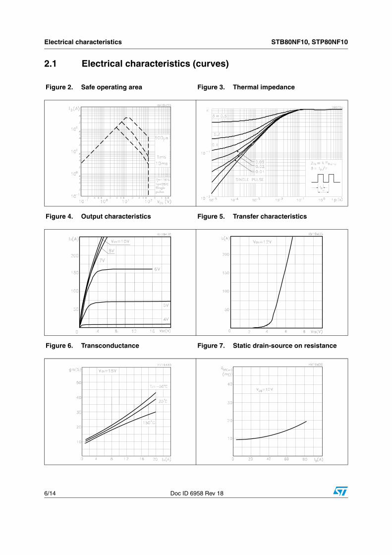
2.1 Electrical characteristics (curves)
Figure 2. Safe operating area Figure 3. Thermal impedance
Figure 4. Output characteristics Figure 5. Transfer characteristics
Figure 6. Transconductance Figure 7. Static drain-source on resistance
STB80NF10, STP80NF10 Electrical characteristics
Doc ID 6958 Rev 18 7/14
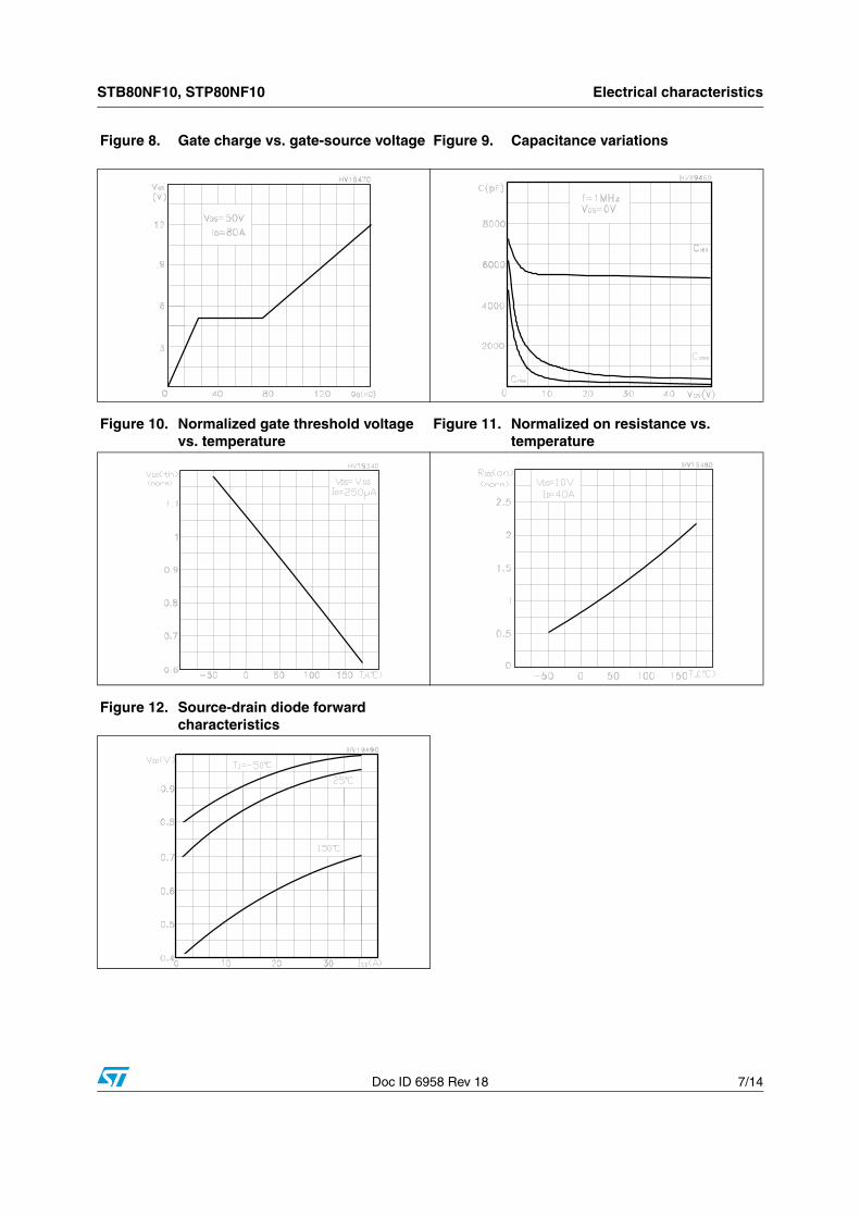
Figure 8. Gate charge vs. gate-source voltage Figure 9. Capacitance variations
Figure 10. Normalized gate threshold voltage vs. temperature
Figure 11. Normalized on resistance vs. temperature
Figure 12. Source-drain diode forward characteristics
Test circuits STB80NF10, STP80NF10
8/14 Doc ID 6958 Rev 18
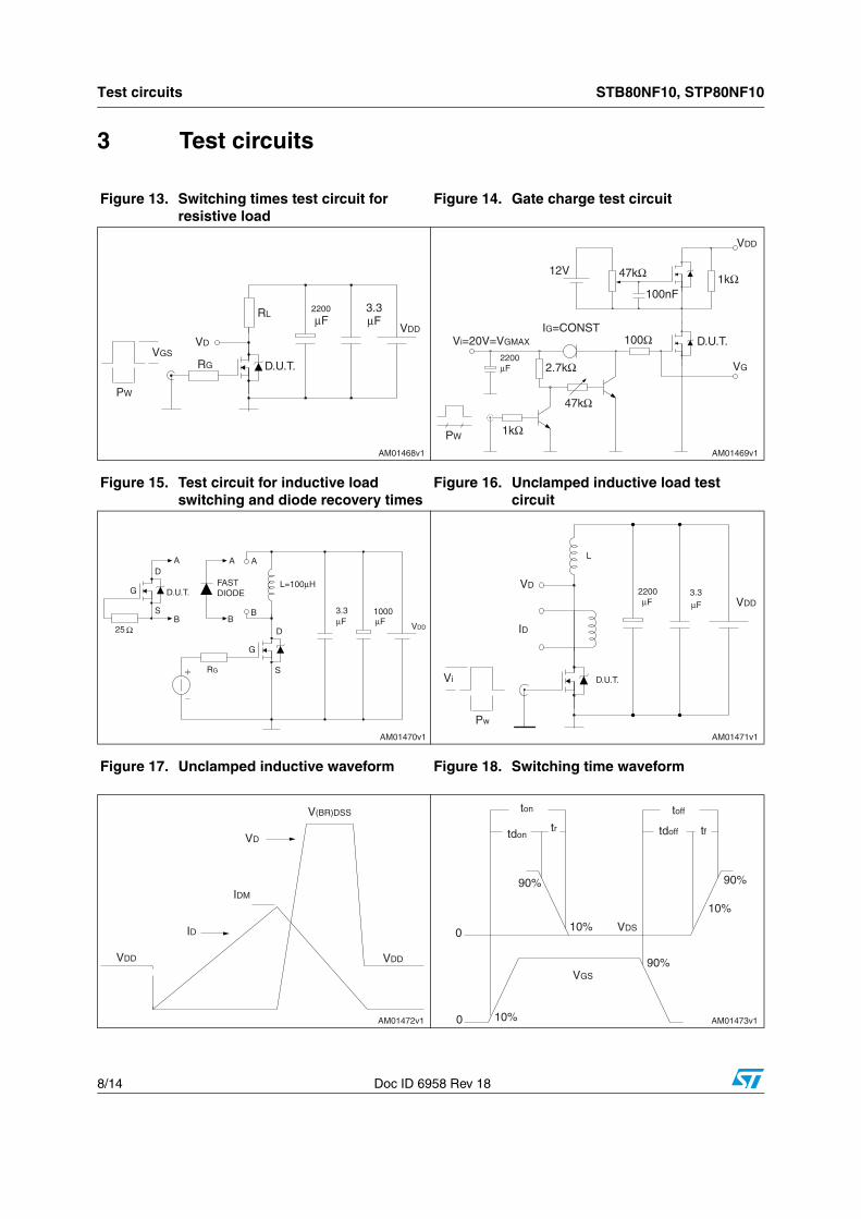
3 Test circuits
Figure 13. Switching times test circuit for resistive load
Figure 14. Gate charge test circuit
Figure 15. Test circuit for inductive load switching and diode recovery times
Figure 16. Unclamped inductive load test circuit
Figure 17. Unclamped inductive waveform Figure 18. Switching time waveform
AM01468v1
VGS
PW
VD
RG
RL
D.U.T.
2200
µF3.3µF
VDD
AM01469v1
VDD
47kΩ 1kΩ
47kΩ
2.7kΩ
1kΩ
12V
Vi=20V=VGMAX
2200µF
PW
IG=CONST100Ω
100nF
D.U.T.
VG
AM01470v1
AD
D.U.T.
SB
G
25 Ω
A A
BB
RG
G
FASTDIODE
D
S
L=100µH
µF3.3 1000
µF VDD
AM01471v1
Vi
Pw
VD
ID
D.U.T.
L
2200µF
3.3µF VDD
AM01472v1
V(BR)DSS
VDDVDD
VD
IDM
ID
AM01473v1
VDS
ton
tdon tdoff
toff
tftr
90%
10%
10%
0
0
90%
90%
10%
VGS
STB80NF10, STP80NF10 Package mechanical data
Doc ID 6958 Rev 18 9/14
4 Package mechanical data
In order to meet environmental requirements, ST offers these devices in different grades of ECOPACK® packages, depending on their level of environmental compliance. ECOPACK® specifications, grade definitions and product status are available at: www.st.com. ECOPACK is an ST trademark.
Package mechanical data STB80NF10, STP80NF10
10/14 Doc ID 6958 Rev 18
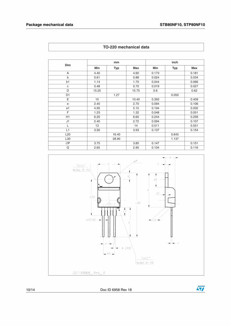
TO-220 mechanical data
Dimmm inch
Min Typ Max Min Typ Max
A 4.40 4.60 0.173 0.181
b 0.61 0.88 0.024 0.034
b1 1.14 1.70 0.044 0.066c 0.48 0.70 0.019 0.027
D 15.25 15.75 0.6 0.62
D1 1.27 0.050E 10 10.40 0.393 0.409
e 2.40 2.70 0.094 0.106
e1 4.95 5.15 0.194 0.202F 1.23 1.32 0.048 0.051
H1 6.20 6.60 0.244 0.256
J1 2.40 2.72 0.094 0.107L 13 14 0.511 0.551
L1 3.50 3.93 0.137 0.154
L20 16.40 0.645L30 28.90 1.137
∅P 3.75 3.85 0.147 0.151
Q 2.65 2.95 0.104 0.116
STB80NF10, STP80NF10 Package mechanical data
Doc ID 6958 Rev 18 11/14
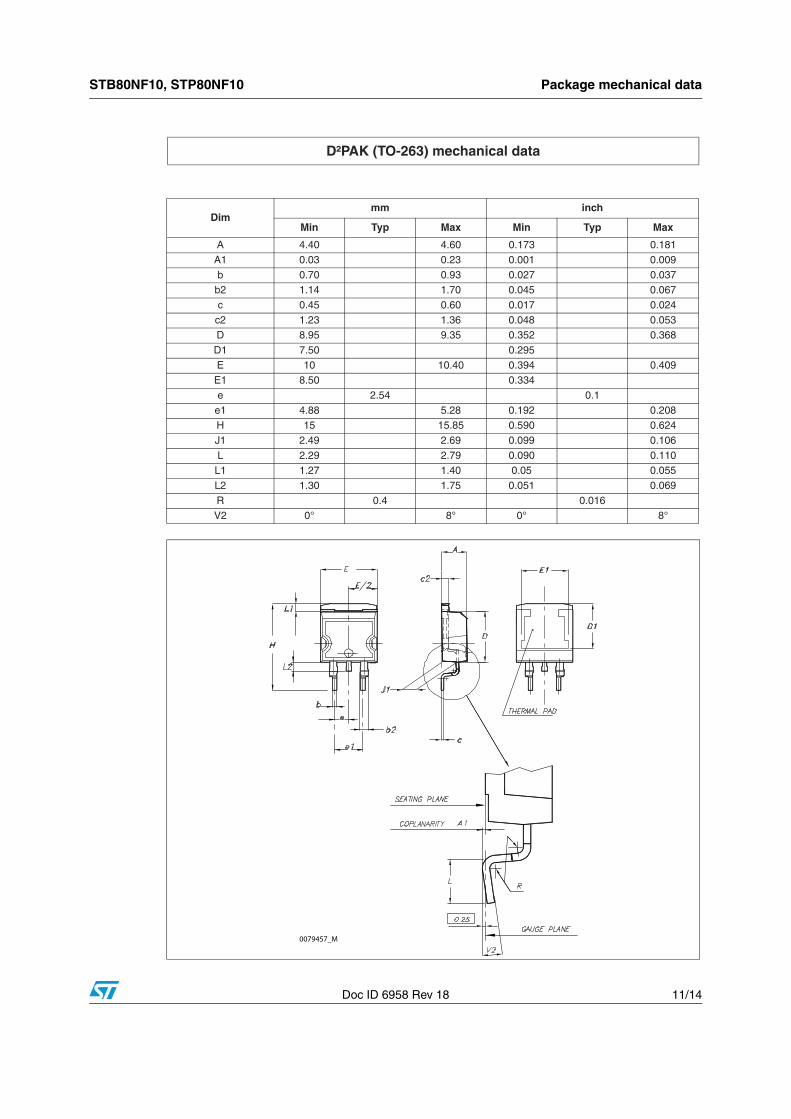
D²PAK (TO-263) mechanical data
Dimmm inch
Min Typ Max Min Typ Max
A 4.40 4.60 0.173 0.181
A1 0.03 0.23 0.001 0.009
b 0.70 0.93 0.027 0.037b2 1.14 1.70 0.045 0.067
c 0.45 0.60 0.017 0.024
c2 1.23 1.36 0.048 0.053D 8.95 9.35 0.352 0.368
D1 7.50 0.295
E 10 10.40 0.394 0.409E1 8.50 0.334
e 2.54 0.1
e1 4.88 5.28 0.192 0.208H 15 15.85 0.590 0.624
J1 2.49 2.69 0.099 0.106
L 2.29 2.79 0.090 0.110L1 1.27 1.40 0.05 0.055
L2 1.30 1.75 0.051 0.069
R 0.4 0.016V2 0° 8° 0° 8°
0079457_M
Packaging mechanical data STB80NF10, STP80NF10
12/14 Doc ID 6958 Rev 18
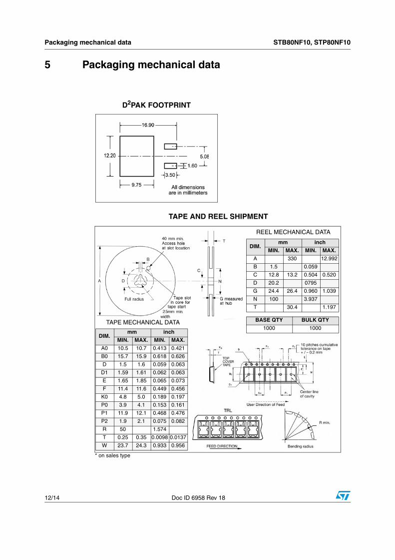
5 Packaging mechanical data
TAPE AND REEL SHIPMENT
D2PAK FOOTPRINT
* on sales type
DIM.mm inch
MIN. MAX. MIN. MAX.
A 330 12.992
B 1.5 0.059
C 12.8 13.2 0.504 0.520
D 20.2 0795
G 24.4 26.4 0.960 1.039
N 100 3.937
T 30.4 1.197
BASE QTY BULK QTY
1000 1000
REEL MECHANICAL DATA
DIM.mm inch
MIN. MAX. MIN. MAX.
A0 10.5 10.7 0.413 0.421
B0 15.7 15.9 0.618 0.626
D 1.5 1.6 0.059 0.063
D1 1.59 1.61 0.062 0.063
E 1.65 1.85 0.065 0.073
F 11.4 11.6 0.449 0.456
K0 4.8 5.0 0.189 0.197
P0 3.9 4.1 0.153 0.161
P1 11.9 12.1 0.468 0.476
P2 1.9 2.1 0.075 0.082
R 50 1.574
T 0.25 0.35 0.0098 0.0137
W 23.7 24.3 0.933 0.956
TAPE MECHANICAL DATA
STB80NF10, STP80NF10 Revision history
Doc ID 6958 Rev 18 13/14
6 Revision history
Table 8. Document revision history
Date Revision Changes
04-Nov-2003 8 New datasheet according to PCN DSG-TRA/03/382
13-Dec-2004 9 D²PAK inserted
16-Dec-2004 10 @ inserted in table 2 for TO-220 marking
27-Jan-2005 11 New value in table 3
22-Feb-2005 12 Id value changed
28-Feb-2005 13 New value in table 3
01-Mar-2005 14 Vgs value changed
06-Apr-2006 15 The document has been reformatted
25-Jan-2007 16 Typo mistake on page 1 (order codes)
17-Nov-2008 17 EAS value has been updated
15-Apr-2009 18 IDSS value changed in Table 4: On/off states
STB80NF10, STP80NF10
14/14 Doc ID 6958 Rev 18
Please Read Carefully:
Information in this document is provided solely in connection with ST products. STMicroelectronics NV and its subsidiaries (“ST”) reserve theright to make changes, corrections, modifications or improvements, to this document, and the products and services described herein at anytime, without notice.
All ST products are sold pursuant to ST’s terms and conditions of sale.
Purchasers are solely responsible for the choice, selection and use of the ST products and services described herein, and ST assumes noliability whatsoever relating to the choice, selection or use of the ST products and services described herein.
No license, express or implied, by estoppel or otherwise, to any intellectual property rights is granted under this document. If any part of thisdocument refers to any third party products or services it shall not be deemed a license grant by ST for the use of such third party productsor services, or any intellectual property contained therein or considered as a warranty covering the use in any manner whatsoever of suchthird party products or services or any intellectual property contained therein.
UNLESS OTHERWISE SET FORTH IN ST’S TERMS AND CONDITIONS OF SALE ST DISCLAIMS ANY EXPRESS OR IMPLIEDWARRANTY WITH RESPECT TO THE USE AND/OR SALE OF ST PRODUCTS INCLUDING WITHOUT LIMITATION IMPLIEDWARRANTIES OF MERCHANTABILITY, FITNESS FOR A PARTICULAR PURPOSE (AND THEIR EQUIVALENTS UNDER THE LAWSOF ANY JURISDICTION), OR INFRINGEMENT OF ANY PATENT, COPYRIGHT OR OTHER INTELLECTUAL PROPERTY RIGHT.
UNLESS EXPRESSLY APPROVED IN WRITING BY AN AUTHORIZED ST REPRESENTATIVE, ST PRODUCTS ARE NOTRECOMMENDED, AUTHORIZED OR WARRANTED FOR USE IN MILITARY, AIR CRAFT, SPACE, LIFE SAVING, OR LIFE SUSTAININGAPPLICATIONS, NOR IN PRODUCTS OR SYSTEMS WHERE FAILURE OR MALFUNCTION MAY RESULT IN PERSONAL INJURY,DEATH, OR SEVERE PROPERTY OR ENVIRONMENTAL DAMAGE. ST PRODUCTS WHICH ARE NOT SPECIFIED AS "AUTOMOTIVEGRADE" MAY ONLY BE USED IN AUTOMOTIVE APPLICATIONS AT USER’S OWN RISK.
Resale of ST products with provisions different from the statements and/or technical features set forth in this document shall immediately voidany warranty granted by ST for the ST product or service described herein and shall not create or extend in any manner whatsoever, anyliability of ST.
ST and the ST logo are trademarks or registered trademarks of ST in various countries.
Information in this document supersedes and replaces all information previously supplied.
The ST logo is a registered trademark of STMicroelectronics. All other names are the property of their respective owners.
© 2009 STMicroelectronics - All rights reserved
STMicroelectronics group of companies
Australia - Belgium - Brazil - Canada - China - Czech Republic - Finland - France - Germany - Hong Kong - India - Israel - Italy - Japan - Malaysia - Malta - Morocco - Philippines - Singapore - Spain - Sweden - Switzerland - United Kingdom - United States of America
www.st.com