N-channel 100 V, 0.008 typ., 80 A STripFET VII DeepGATE ... · This is information on a product in...
25
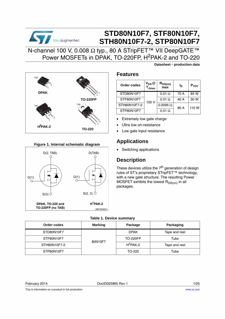
This is information on a product in full production. February 2014 DocID025865 Rev 1 1/25 STD80N10F7, STF80N10F7, STH80N10F7-2, STP80N10F7 N-channel 100 V, 0.008 Ω typ., 80 A STripFET™ VII DeepGATE™ Power MOSFETs in DPAK, TO-220FP, H 2 PAK-2 and TO-220 Datasheet - production data Figure 1. Internal schematic diagram Features • Extremely low gate charge • Ultra low on-resistance • Low gate input resistance Applications • Switching applications Description These devices utilize the 7 th generation of design rules of ST’s proprietary STripFET™ technology, with a new gate structure. The resulting Power MOSFET exhibits the lowest R DS(on) in all packages. TO-220 DPAK H PAK-2 2 1 3 TAB 1 2 3 TAB 1 3 2 TAB 1 2 3 TO-220FP Order codes V DS @ T Jmax R DS(on) max I D P TOT STD80N10F7 100 V 0.01 Ω 70 A 85 W STF80N10F7 0.01 Ω 40 A 30 W STH80N10F7-2 0.0095 Ω 80 A 110 W STP80N10F7 0.01 Ω Table 1. Device summary Order codes Marking Package Packaging STD80N10F7 80N10F7 DPAK Tape and reel STF80N10F7 TO-220FP Tube STH80N10F7-2 H 2 PAK-2 Tape and reel STP80N10F7 TO-220 Tube www.st.com
Transcript of N-channel 100 V, 0.008 typ., 80 A STripFET VII DeepGATE ... · This is information on a product in...
This is information on a product in full production.
February 2014 DocID025865 Rev 1 1/25
STD80N10F7, STF80N10F7, STH80N10F7-2, STP80N10F7
N-channel 100 V, 0.008 Ω typ., 80 A STripFET™ VII DeepGATE™
Power MOSFETs in DPAK, TO-220FP, H2PAK-2 and TO-220
Datasheet - production data
Figure 1. Internal schematic diagram
Features
• Extremely low gate charge
• Ultra low on-resistance
• Low gate input resistance
Applications• Switching applications
DescriptionThese devices utilize the 7
th generation of design
rules of ST’s proprietary STripFET™ technology,
with a new gate structure. The resulting Power
MOSFET exhibits the lowest RDS(on)
in all
packages.
TO-220
DPAK
H PAK-22
1
3
TAB
12
3
TAB
13
2
TAB
123
TO-220FP
Order codesVDS @ TJmax
RDS(on) max
ID PTOT
STD80N10F7
100 V
0.01 Ω 70 A 85 W
STF80N10F7 0.01 Ω 40 A 30 W
STH80N10F7-2 0.0095 Ω80 A 110 W
STP80N10F7 0.01 Ω
Table 1. Device summary
Order codes Marking Package Packaging
STD80N10F7
80N10F7
DPAK Tape and reel
STF80N10F7 TO-220FP Tube
STH80N10F7-2 H2PAK-2 Tape and reel
STP80N10F7 TO-220 Tube
www.st.com
Contents STD80N10F7, STF80N10F7, STH80N10F7-2, STP80N10F7
2/25 DocID025865 Rev 1
Contents
1 Electrical ratings . . . . . . . . . . . . . . . . . . . . . . . . . . . . . . . . . . . . . . . . . . . . 3
2 Electrical characteristics . . . . . . . . . . . . . . . . . . . . . . . . . . . . . . . . . . . . . 4
2.1 Electrical characteristics (curves) . . . . . . . . . . . . . . . . . . . . . . . . . . . . . . . . 6
3 Test circuits . . . . . . . . . . . . . . . . . . . . . . . . . . . . . . . . . . . . . . . . . . . . . . 9
4 Package mechanical data . . . . . . . . . . . . . . . . . . . . . . . . . . . . . . . . . . . . 10
5 Packaging mechanical data . . . . . . . . . . . . . . . . . . . . . . . . . . . . . . . . . . 21
6 Revision history . . . . . . . . . . . . . . . . . . . . . . . . . . . . . . . . . . . . . . . . . . . 24
DocID025865 Rev 1 3/25
STD80N10F7, STF80N10F7, STH80N10F7-2, STP80N10F7 Electrical ratings
25
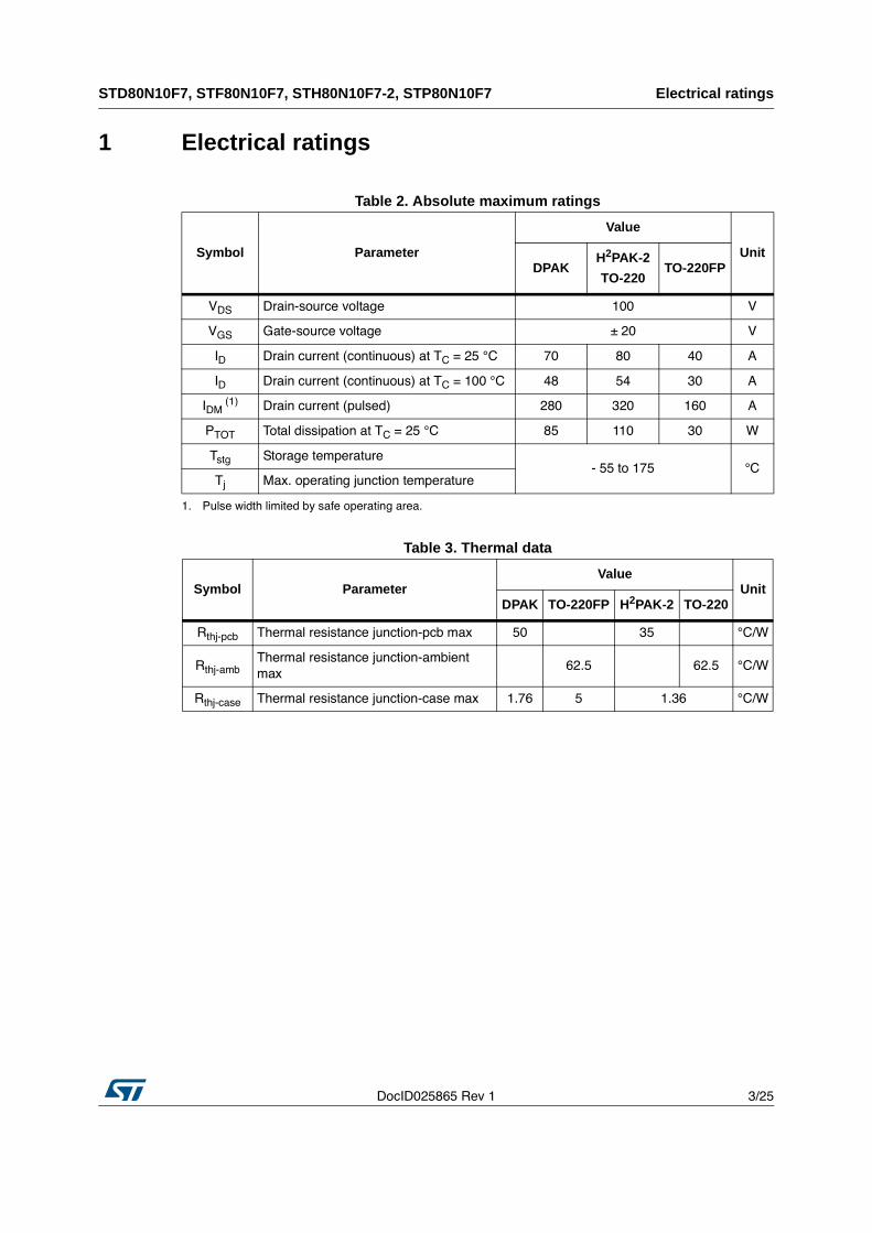
1 Electrical ratings
Table 2. Absolute maximum ratings
Symbol Parameter
Value
UnitDPAK
H2PAK-2
TO-220TO-220FP
VDS
Drain-source voltage 100 V
VGS
Gate-source voltage ± 20 V
ID
Drain current (continuous) at TC
= 25 °C 70 80 40 A
ID
Drain current (continuous) at TC
= 100 °C 48 54 30 A
IDM
(1)
1. Pulse width limited by safe operating area.
Drain current (pulsed) 280 320 160 A
PTOT
Total dissipation at TC
= 25 °C 85 110 30 W
Tstg
Storage temperature
- 55 to 175 °C
Tj
Max. operating junction temperature
Table 3. Thermal data
Symbol ParameterValue
UnitDPAK TO-220FP H2PAK-2 TO-220
Rthj-pcb
Thermal resistance junction-pcb max 50 35 °C/W
Rthj-amb
Thermal resistance junction-ambient
max
62.5 62.5 °C/W
Rthj-case
Thermal resistance junction-case max 1.76 5 1.36 °C/W
Electrical characteristics STD80N10F7, STF80N10F7, STH80N10F7-2, STP80N10F7
4/25 DocID025865 Rev 1
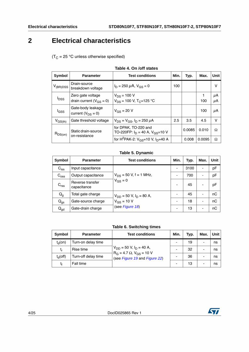
2 Electrical characteristics
(TC
= 25 °C unless otherwise specified)
Table 4. On /off states
Symbol Parameter Test conditions Min. Typ. Max. Unit
V(BR)DSS
Drain-source
breakdown voltage
ID
= 250 μA, VGS
= 0 100 V
IDSS
Zero gate voltage
drain current (VGS
= 0)
VDS
= 100 V
VDS
= 100 V, TC
=125 °C
1
100
μA
μA
IGSS
Gate-body leakage
current (VDS
= 0)
VGS
= 20 V 100 μA
VGS(th)
Gate threshold voltage VDS
= VGS
, ID
= 250 μA 2.5 3.5 4.5 V
RDS(on)
Static drain-source
on-resistance
for DPAK, TO-220 and
TO-220FP: ID
= 40 A, VGS
=10 V
0.0085 0.010 Ω
for H2PAK-2: V
GS=10 V, I
D=40 A 0.008 0.0095 Ω
Table 5. Dynamic
Symbol Parameter Test conditions Min. Typ. Max. Unit
Ciss
Input capacitance
VDS
= 50 V, f = 1 MHz,
VGS
= 0
- 3100 - pF
Coss
Output capacitance - 700 - pF
Crss
Reverse transfer
capacitance
- 45 - pF
Qg
Total gate chargeV
DD = 50 V, I
D = 80 A,
VGS
= 10 V
(see Figure 18)
- 45 - nC
Qgs
Gate-source charge - 18 - nC
Qgd
Gate-drain charge - 13 - nC
Table 6. Switching times
Symbol Parameter Test conditions Min. Typ. Max. Unit
td(on) Turn-on delay time
VDD
= 50 V, ID
= 40 A,
RG
= 4.7 Ω, VGS
= 10 V
(see Figure 19 and Figure 22)
- 19 - ns
tr
Rise time - 32 - ns
td(off) Turn-off delay time - 36 - ns
tf
Fall time - 13 - ns
DocID025865 Rev 1 5/25
STD80N10F7, STF80N10F7, STH80N10F7-2, STP80N10F7 Electrical characteristics
25
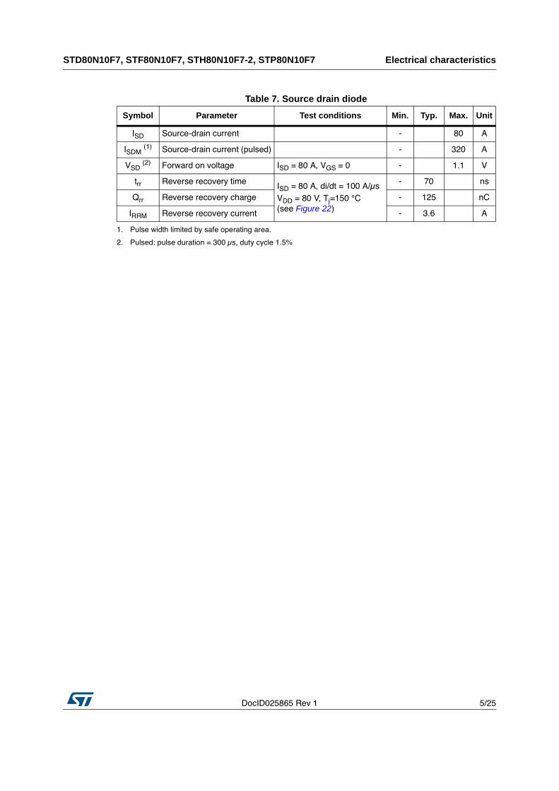
Table 7. Source drain diode
Symbol Parameter Test conditions Min. Typ. Max. Unit
ISD
Source-drain current - 80 A
ISDM
(1)
1. Pulse width limited by safe operating area.
Source-drain current (pulsed) - 320 A
VSD
(2)
2. Pulsed: pulse duration = 300 μs, duty cycle 1.5%
Forward on voltage ISD
= 80 A, VGS
= 0 - 1.1 V
trr
Reverse recovery timeISD
= 80 A, di/dt = 100 A/μs
VDD
= 80 V, Tj=150 °C
(see Figure 22)
- 70 ns
Qrr
Reverse recovery charge - 125 nC
IRRM
Reverse recovery current - 3.6 A
Electrical characteristics STD80N10F7, STF80N10F7, STH80N10F7-2, STP80N10F7
6/25 DocID025865 Rev 1
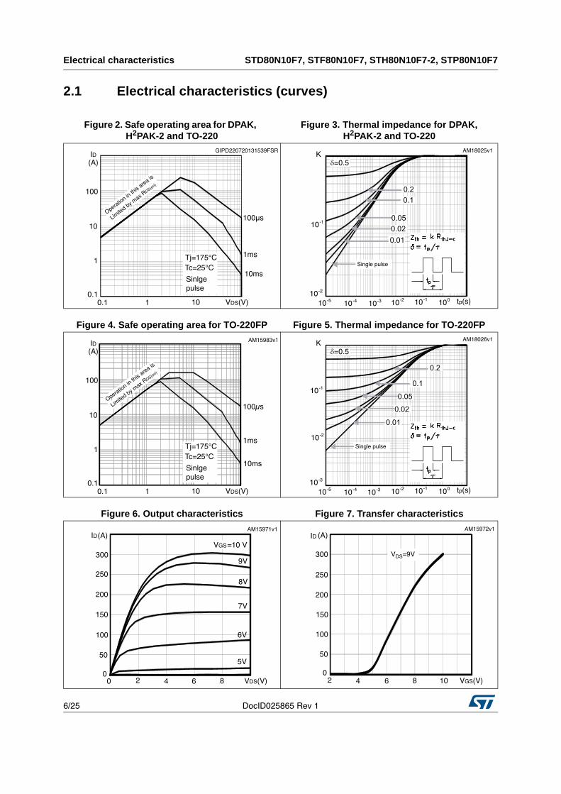
2.1 Electrical characteristics (curves)
Figure 2. Safe operating area for DPAK, H2PAK-2 and TO-220
Figure 3. Thermal impedance for DPAK, H2PAK-2 and TO-220
ID
100
10
1
0.10.1 1 VDS(V)10
(A)
Operation in
this
area is
Limite
d by max R
DS(on)
100µs
1msTj=175°CTc=25°C
Sinlgepulse
10ms
GIPD220720131539FSR
Single pulse
δ=0.5
0.050.020.01
0.10.2
K
10 tp(s)-4 10-3
10-1
10-510-2
10-2 10-1 100
c
AM18025v1
Figure 4. Safe operating area for TO-220FP Figure 5. Thermal impedance for TO-220FP
ID
100
10
1
0.10.1 1 VDS(V)10
(A)
Operation in
this
area is
Limite
d by max R
DS(on)
100µs
1msTj=175°CTc=25°C
Sinlgepulse
10ms
AM15983v1
Single pulse
δ=0.5
0.05
0.02
0.01
0.1
0.2
K
10 tp(s)-4 10-3
10-2
10-510-3
10-2 10-1 100
c
10-1
AM18026v1
Figure 6. Output characteristics Figure 7. Transfer characteristics
ID
300
200
100
00 4 VDS(V)8
(A)
2 6
5V
250
150
50
6V
7V
8V
9V
VGS=10 V
AM15971v1ID
300
200
100
04 VGS(V)8
(A)
2 6
50
150
250
VDS=9V
10
AM15972v1
DocID025865 Rev 1 7/25
STD80N10F7, STF80N10F7, STH80N10F7-2, STP80N10F7 Electrical characteristics
25
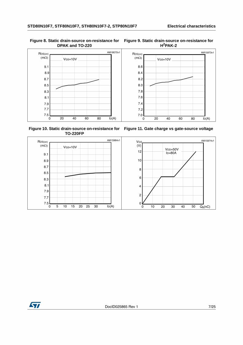
Figure 8. Static drain-source on-resistance for DPAK and TO-220
Figure 9. Static drain-source on-resistance for H2PAK-2
RDS(on)
8.1
7.9
7.7
7.50 80 ID(A)
(mΩ)
40
8.3
8.5
VGS=10V
20 60
8.7
8.9
9.1
AM18070v1 RDS(on)
7.6
7.4
7.2
7.00 80 ID(A)
(mΩ)
40
7.8
8.0
VGS=10V
20 60
8.2
8.4
8.6
AM15973v1
Figure 10. Static drain-source on-resistance for TO-220FP
Figure 11. Gate charge vs gate-source voltage
RDS(on)
8.1
7.9
7.7
7.50 20 ID(A)
(mΩ)
10
8.3
VGS=10V
5 15
8.5
25 30
8.7
8.9
9.1
AM15984v1 VGS
6
4
2
00 10 Qg(nC)
(V)
40
8
20 30
10
VDD=50VID=80A12
50
AM15974v1
Electrical characteristics STD80N10F7, STF80N10F7, STH80N10F7-2, STP80N10F7
8/25 DocID025865 Rev 1
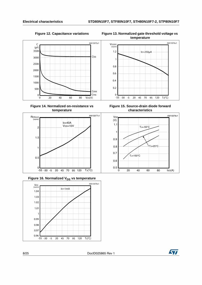
Figure 12. Capacitance variations Figure 13. Normalized gate threshold voltage vs temperature
C
1500
1000
500
00 40 VDS(V)
(pF)
20
2000
60
Ciss
CossCrss
80
2500
3000
3500
AM15975v1 VGS(th)
0.8
0.6
0.4
0.2
-55 -5 TJ(°C)
(norm)
-30
1
7020 45 95
ID=250µA
0120
1.2
AM15976v1
Figure 14. Normalized on-resistance vs temperature
Figure 15. Source-drain diode forward characteristics
Figure 16. Normalized VDS vs temperature
RDS(on)
0.5
0TJ(°C)
(norm)
ID=40A
1
-55 -5-30 7020 45 95 120
1.5
2VGS=10V
AM15977v1 VSD
0 40 ISD(A)
(V)
20 60 80
0.6
0.7
0.8
0.9
TJ=-55°C
TJ=150°C
TJ=25°C
0.5
1
1.1
AM15978v1
VDS
TJ(°C)
(norm)
0.96
0.97
0.98
0.99
1
ID=1mA
-55 -5-30 7020 45 95 120
1.01
1.02
1.03
1.04
AM15979v1
DocID025865 Rev 1 9/25
STD80N10F7, STF80N10F7, STH80N10F7-2, STP80N10F7 Test circuits
25
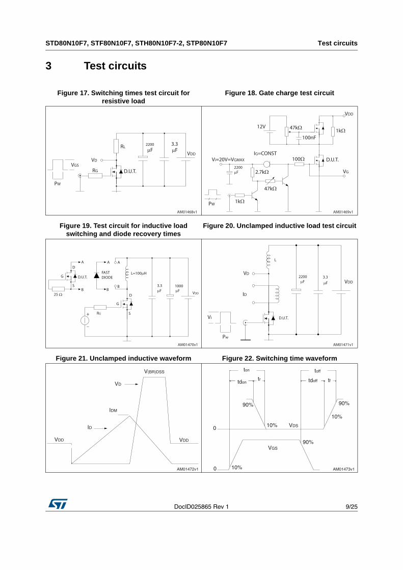
3 Test circuits
Figure 17. Switching times test circuit for resistive load
Figure 18. Gate charge test circuit
Figure 19. Test circuit for inductive load switching and diode recovery times
Figure 20. Unclamped inductive load test circuit
Figure 21. Unclamped inductive waveform Figure 22. Switching time waveform
AM01468v1
VGS
PW
VD
RG
RL
D.U.T.
2200
μF3.3μF
VDD
AM01469v1
VDD
47kΩ 1kΩ
47kΩ
2.7kΩ
1kΩ
12V
Vi=20V=VGMAX
2200μF
PW
IG=CONST100Ω
100nF
D.U.T.
VG
AM01470v1
AD
D.U.T.
SB
G
25 Ω
A A
BB
RG
G
FASTDIODE
D
S
L=100μH
μF3.3 1000
μF VDD
AM01471v1
Vi
Pw
VD
ID
D.U.T.
L
2200μF
3.3μF VDD
AM01472v1
V(BR)DSS
VDDVDD
VD
IDM
ID
AM01473v1
VDS
ton
tdon tdoff
toff
tftr
90%
10%
10%
0
0
90%
90%
10%
VGS
Package mechanical data STD80N10F7, STF80N10F7, STH80N10F7-2, STP80N10F7
10/25 DocID025865 Rev 1
4 Package mechanical data
In order to meet environmental requirements, ST offers these devices in different grades of
ECOPACK®
packages, depending on their level of environmental compliance. ECOPACK®
specifications, grade definitions and product status are available at: www.st.com.
ECOPACK®
is an ST trademark.
DocID025865 Rev 1 11/25
STD80N10F7, STF80N10F7, STH80N10F7-2, STP80N10F7 Package mechanical data
25
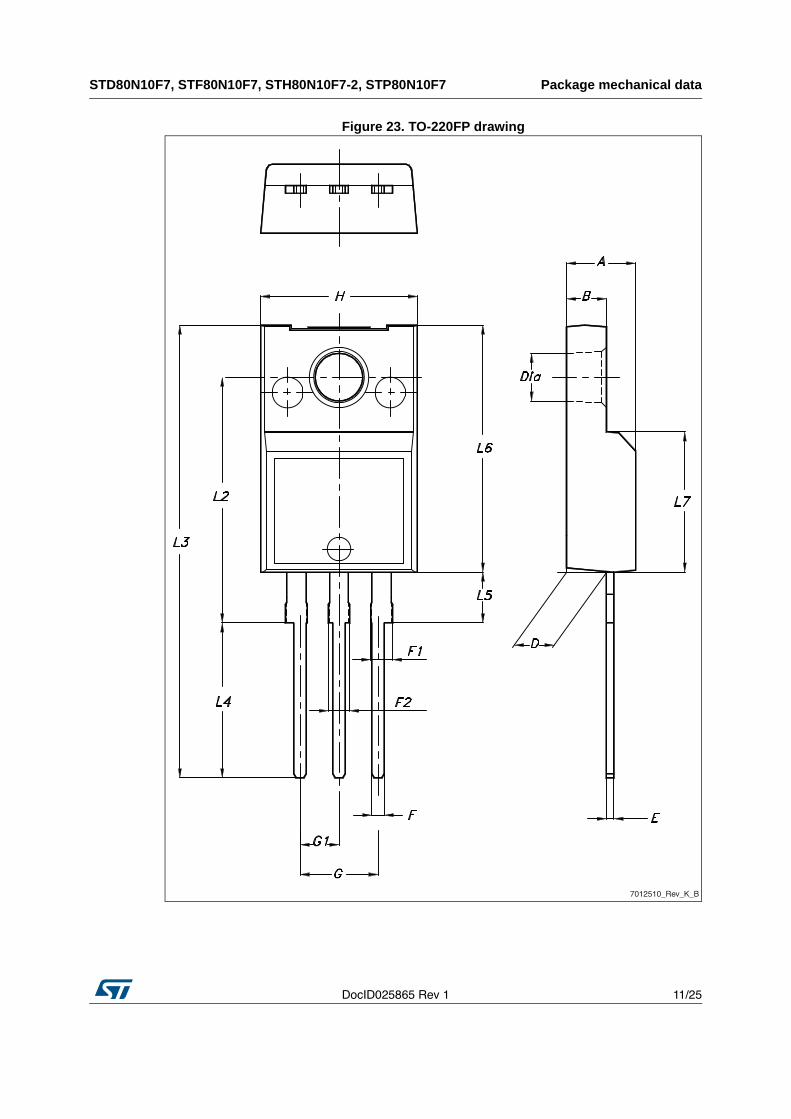
Figure 23. TO-220FP drawing
7012510_Rev_K_B
Package mechanical data STD80N10F7, STF80N10F7, STH80N10F7-2, STP80N10F7
12/25 DocID025865 Rev 1
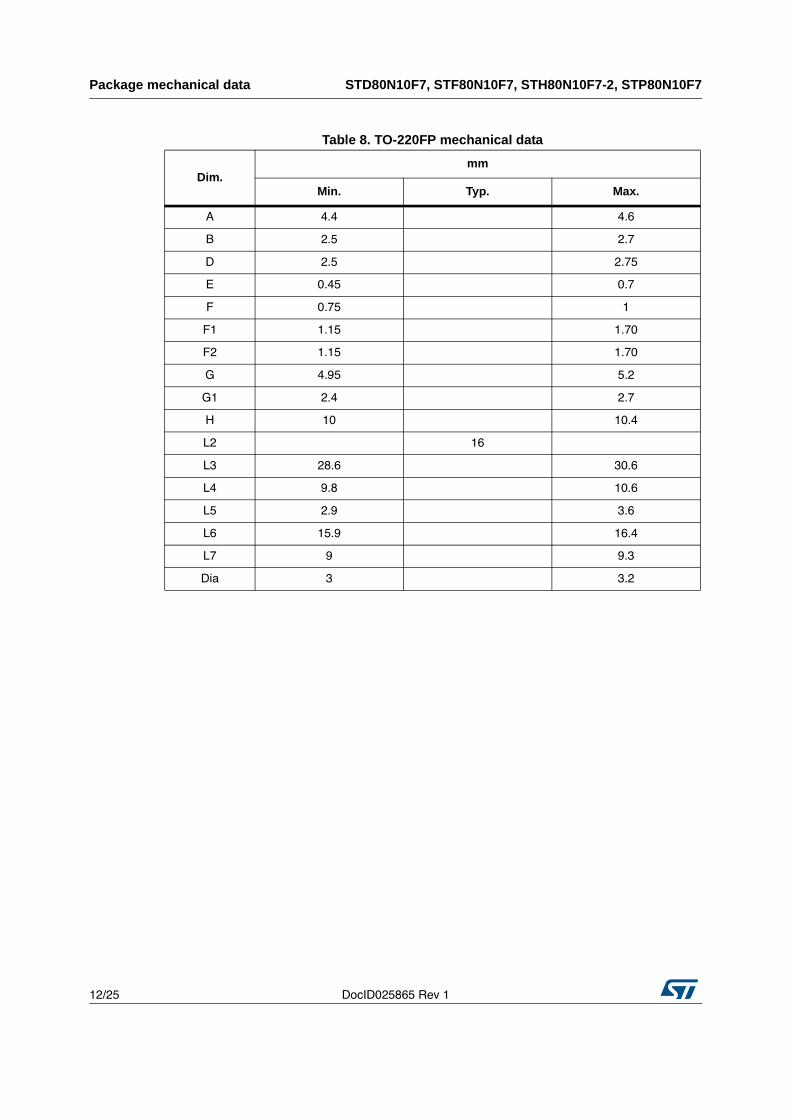
Table 8. TO-220FP mechanical data
Dim.mm
Min. Typ. Max.
A 4.4 4.6
B 2.5 2.7
D 2.5 2.75
E 0.45 0.7
F 0.75 1
F1 1.15 1.70
F2 1.15 1.70
G 4.95 5.2
G1 2.4 2.7
H 10 10.4
L2 16
L3 28.6 30.6
L4 9.8 10.6
L5 2.9 3.6
L6 15.9 16.4
L7 9 9.3
Dia 3 3.2
DocID025865 Rev 1 13/25
STD80N10F7, STF80N10F7, STH80N10F7-2, STP80N10F7 Package mechanical data
25
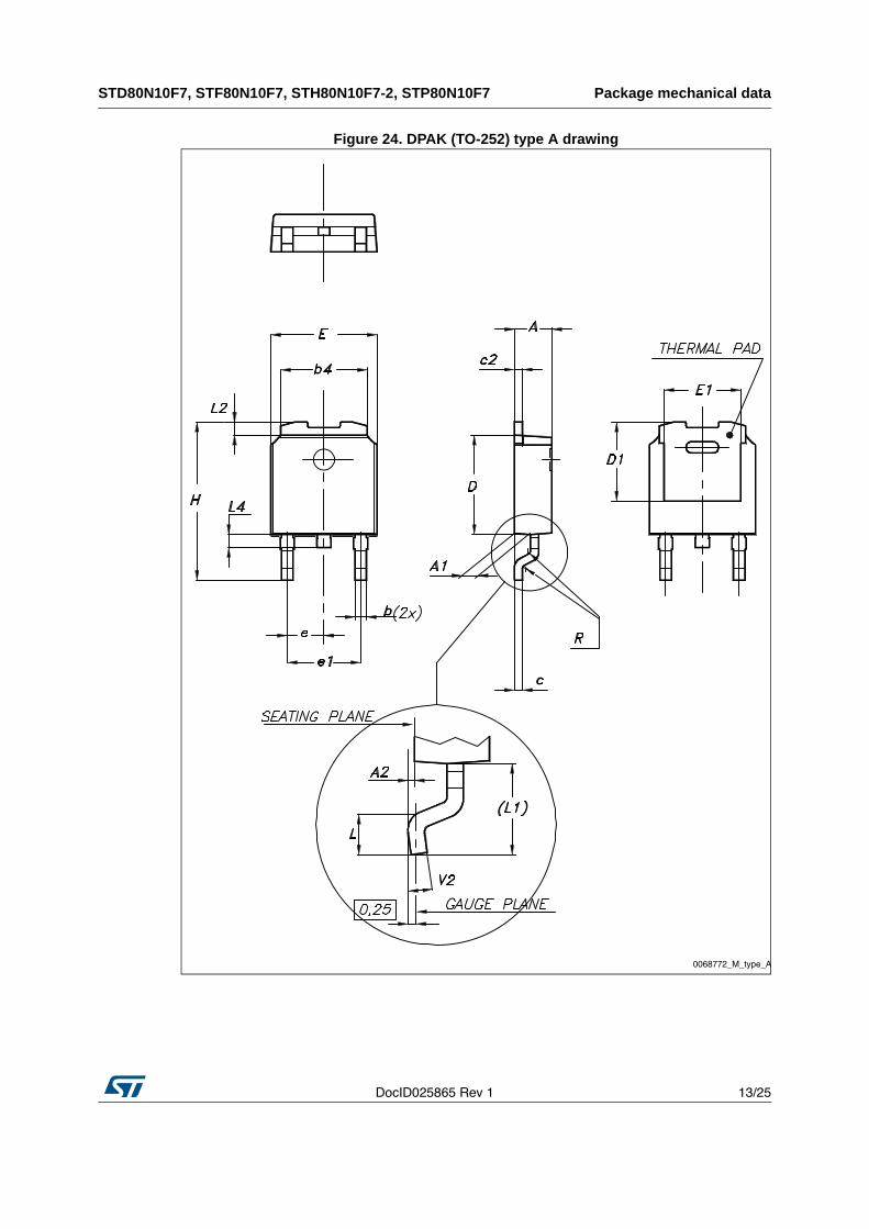
Figure 24. DPAK (TO-252) type A drawing
0068772_M_type_A
Package mechanical data STD80N10F7, STF80N10F7, STH80N10F7-2, STP80N10F7
14/25 DocID025865 Rev 1
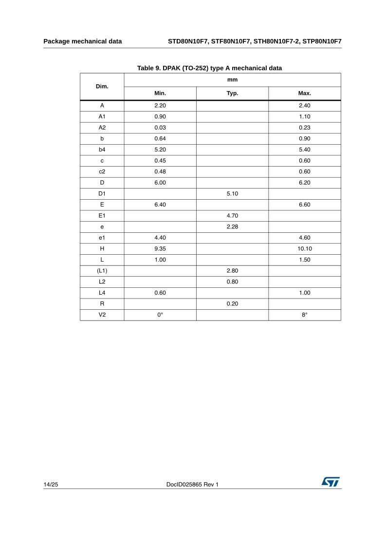
Table 9. DPAK (TO-252) type A mechanical data
Dim.mm
Min. Typ. Max.
A 2.20 2.40
A1 0.90 1.10
A2 0.03 0.23
b 0.64 0.90
b4 5.20 5.40
c 0.45 0.60
c2 0.48 0.60
D 6.00 6.20
D1 5.10
E 6.40 6.60
E1 4.70
e 2.28
e1 4.40 4.60
H 9.35 10.10
L 1.00 1.50
(L1) 2.80
L2 0.80
L4 0.60 1.00
R 0.20
V2 0° 8°
DocID025865 Rev 1 15/25
STD80N10F7, STF80N10F7, STH80N10F7-2, STP80N10F7 Package mechanical data
25
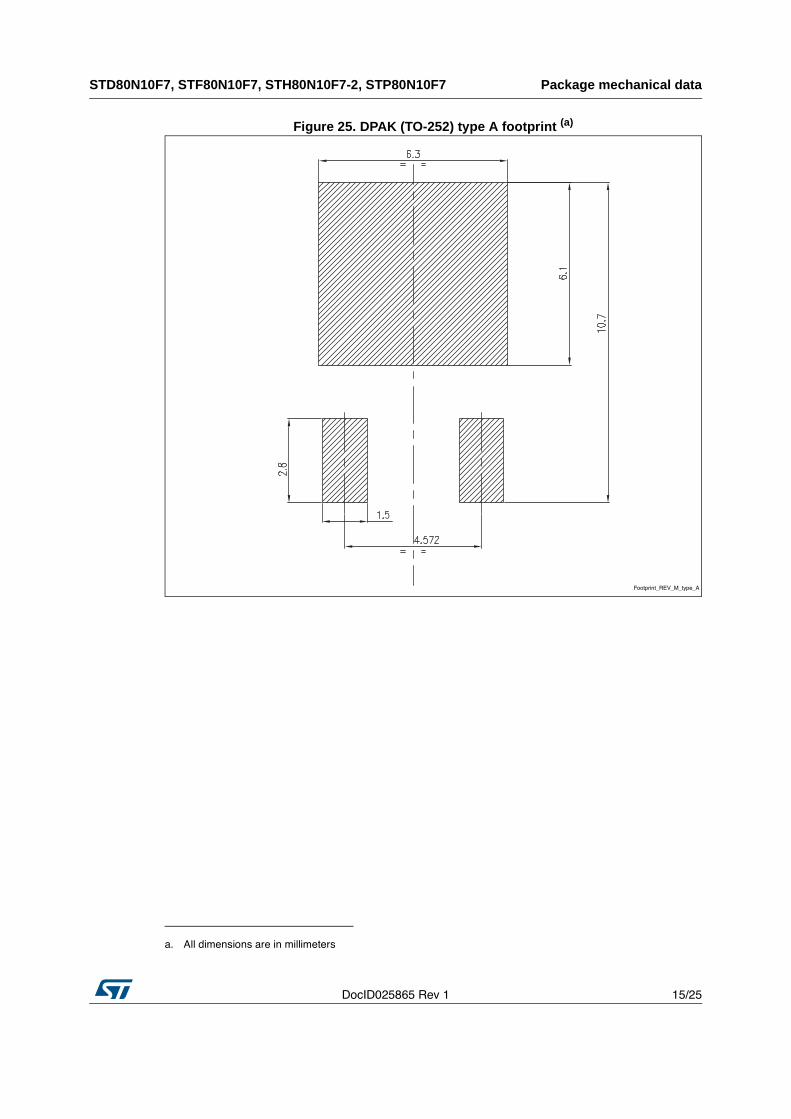
Figure 25. DPAK (TO-252) type A footprint (a)
a. All dimensions are in millimeters
Footprint_REV_M_type_A
Package mechanical data STD80N10F7, STF80N10F7, STH80N10F7-2, STP80N10F7
16/25 DocID025865 Rev 1
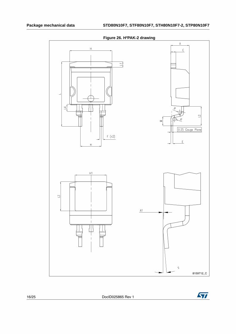
Figure 26. H²PAK-2 drawing
8159712_C
DocID025865 Rev 1 17/25
STD80N10F7, STF80N10F7, STH80N10F7-2, STP80N10F7 Package mechanical data
25
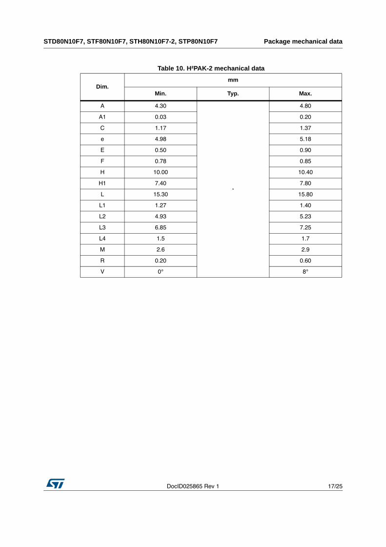
Table 10. H²PAK-2 mechanical data
Dim.mm
Min. Typ. Max.
A 4.30
-
4.80
A1 0.03 0.20
C 1.17 1.37
e 4.98 5.18
E 0.50 0.90
F 0.78 0.85
H 10.00 10.40
H1 7.40 7.80
L 15.30 15.80
L1 1.27 1.40
L2 4.93 5.23
L3 6.85 7.25
L4 1.5 1.7
M 2.6 2.9
R 0.20 0.60
V 0° 8°
Package mechanical data STD80N10F7, STF80N10F7, STH80N10F7-2, STP80N10F7
18/25 DocID025865 Rev 1
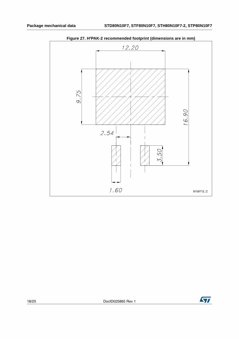
Figure 27. H²PAK-2 recommended footprint (dimensions are in mm)
8159712_C
DocID025865 Rev 1 19/25
STD80N10F7, STF80N10F7, STH80N10F7-2, STP80N10F7 Package mechanical data
25
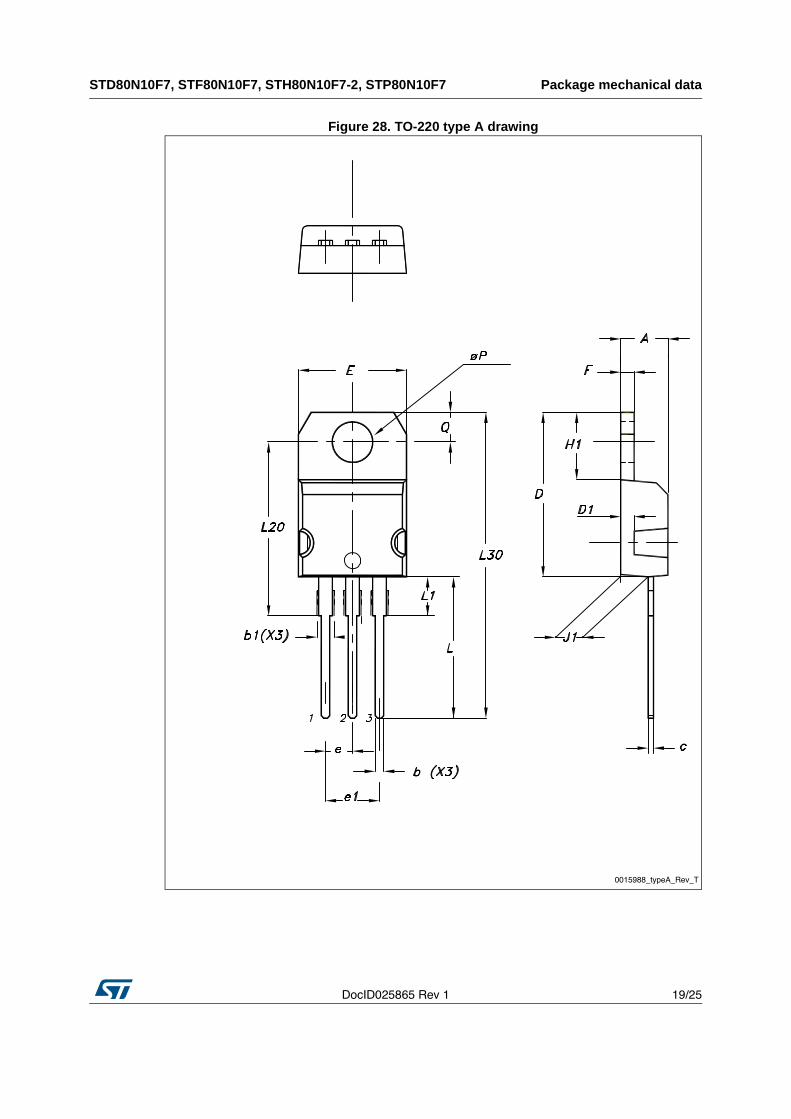
Figure 28. TO-220 type A drawing
Package mechanical data STD80N10F7, STF80N10F7, STH80N10F7-2, STP80N10F7
20/25 DocID025865 Rev 1
Table 11. TO-220 type A mechanical data
Dim.mm
Min. Typ. Max.
A 4.40 4.60
b 0.61 0.88
b1 1.14 1.70
c 0.48 0.70
D 15.25 15.75
D1 1.27
E 10 10.40
e 2.40 2.70
e1 4.95 5.15
F 1.23 1.32
H1 6.20 6.60
J1 2.40 2.72
L 13 14
L1 3.50 3.93
L20 16.40
L30 28.90
∅P 3.75 3.85
Q 2.65 2.95
DocID025865 Rev 1 21/25
STD80N10F7, STF80N10F7, STH80N10F7-2, STP80N10F7 Packaging mechanical data
25
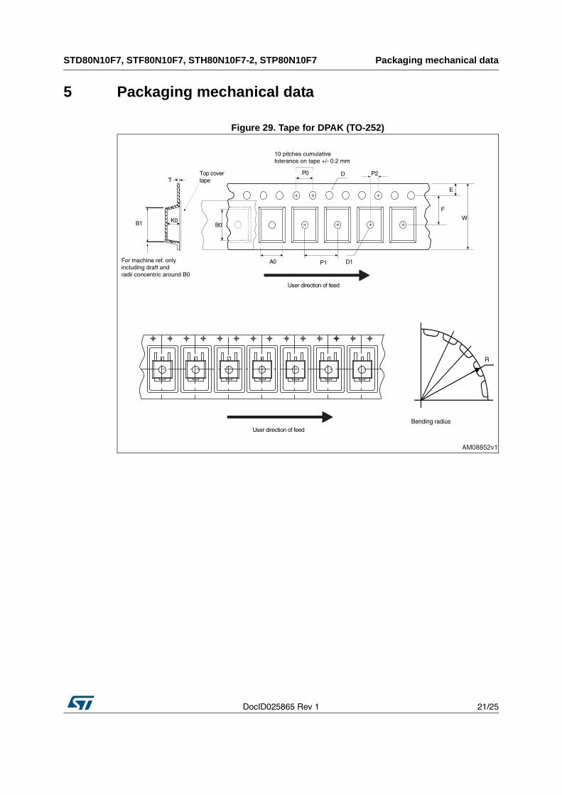
5 Packaging mechanical data
Figure 29. Tape for DPAK (TO-252)
P1A0 D1
P0
F
W
E
D
B0K0
T
User direction of feed
P2
10 pitches cumulativetolerance on tape +/- 0.2 mm
User direction of feed
R
Bending radius
B1
For machine ref. onlyincluding draft andradii concentric around B0
AM08852v1
Top covertape
Packaging mechanical data STD80N10F7, STF80N10F7, STH80N10F7-2, STP80N10F7
22/25 DocID025865 Rev 1
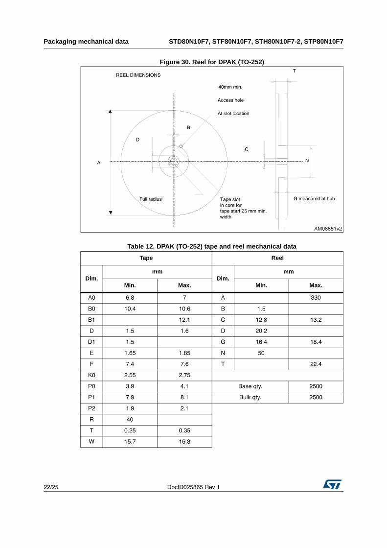
Figure 30. Reel for DPAK (TO-252)
Table 12. DPAK (TO-252) tape and reel mechanical data
Tape Reel
Dim.mm
Dim.mm
Min. Max. Min. Max.
A0 6.8 7 A 330
B0 10.4 10.6 B 1.5
B1 12.1 C 12.8 13.2
D 1.5 1.6 D 20.2
D1 1.5 G 16.4 18.4
E 1.65 1.85 N 50
F 7.4 7.6 T 22.4
K0 2.55 2.75
P0 3.9 4.1 Base qty. 2500
P1 7.9 8.1 Bulk qty. 2500
P2 1.9 2.1
R 40
T 0.25 0.35
W 15.7 16.3
A
D
B
Full radius G measured at hub
C
N
REEL DIMENSIONS
40mm min.
Access hole
At slot location
T
Tape slot in core fortape start 25 mm min.width
AM08851v2
DocID025865 Rev 1 23/25
STD80N10F7, STF80N10F7, STH80N10F7-2, STP80N10F7 Packaging mechanical data
25
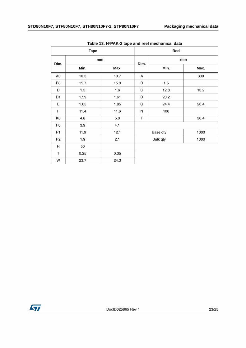
Table 13. H²PAK-2 tape and reel mechanical data
Tape Reel
Dim.mm
Dim.mm
Min. Max. Min. Max.
A0 10.5 10.7 A 330
B0 15.7 15.9 B 1.5
D 1.5 1.6 C 12.8 13.2
D1 1.59 1.61 D 20.2
E 1.65 1.85 G 24.4 26.4
F 11.4 11.6 N 100
K0 4.8 5.0 T 30.4
P0 3.9 4.1
P1 11.9 12.1 Base qty 1000
P2 1.9 2.1 Bulk qty 1000
R 50
T 0.25 0.35
W 23.7 24.3
Revision history STD80N10F7, STF80N10F7, STH80N10F7-2, STP80N10F7
24/25 DocID025865 Rev 1
6 Revision history
Table 14. Document revision history
Date Revision Changes
07-Feb-2014 1 First release.
DocID025865 Rev 1 25/25
STD80N10F7, STF80N10F7, STH80N10F7-2, STP80N10F7
25
Please Read Carefully:
Information in this document is provided solely in connection with ST products. STMicroelectronics NV and its subsidiaries (“ST”) reserve the
right to make changes, corrections, modifications or improvements, to this document, and the products and services described herein at any
time, without notice.
All ST products are sold pursuant to ST’s terms and conditions of sale.
Purchasers are solely responsible for the choice, selection and use of the ST products and services described herein, and ST assumes no
liability whatsoever relating to the choice, selection or use of the ST products and services described herein.
No license, express or implied, by estoppel or otherwise, to any intellectual property rights is granted under this document. If any part of this
document refers to any third party products or services it shall not be deemed a license grant by ST for the use of such third party products
or services, or any intellectual property contained therein or considered as a warranty covering the use in any manner whatsoever of such
third party products or services or any intellectual property contained therein.
UNLESS OTHERWISE SET FORTH IN ST’S TERMS AND CONDITIONS OF SALE ST DISCLAIMS ANY EXPRESS OR IMPLIEDWARRANTY WITH RESPECT TO THE USE AND/OR SALE OF ST PRODUCTS INCLUDING WITHOUT LIMITATION IMPLIEDWARRANTIES OF MERCHANTABILITY, FITNESS FOR A PARTICULAR PURPOSE (AND THEIR EQUIVALENTS UNDER THE LAWSOF ANY JURISDICTION), OR INFRINGEMENT OF ANY PATENT, COPYRIGHT OR OTHER INTELLECTUAL PROPERTY RIGHT.
ST PRODUCTS ARE NOT DESIGNED OR AUTHORIZED FOR USE IN: (A) SAFETY CRITICAL APPLICATIONS SUCH AS LIFESUPPORTING, ACTIVE IMPLANTED DEVICES OR SYSTEMS WITH PRODUCT FUNCTIONAL SAFETY REQUIREMENTS; (B)AERONAUTIC APPLICATIONS; (C) AUTOMOTIVE APPLICATIONS OR ENVIRONMENTS, AND/OR (D) AEROSPACE APPLICATIONSOR ENVIRONMENTS. WHERE ST PRODUCTS ARE NOT DESIGNED FOR SUCH USE, THE PURCHASER SHALL USE PRODUCTS ATPURCHASER’S SOLE RISK, EVEN IF ST HAS BEEN INFORMED IN WRITING OF SUCH USAGE, UNLESS A PRODUCT ISEXPRESSLY DESIGNATED BY ST AS BEING INTENDED FOR “AUTOMOTIVE, AUTOMOTIVE SAFETY OR MEDICAL” INDUSTRYDOMAINS ACCORDING TO ST PRODUCT DESIGN SPECIFICATIONS. PRODUCTS FORMALLY ESCC, QML OR JAN QUALIFIED AREDEEMED SUITABLE FOR USE IN AEROSPACE BY THE CORRESPONDING GOVERNMENTAL AGENCY.
Resale of ST products with provisions different from the statements and/or technical features set forth in this document shall immediately void
any warranty granted by ST for the ST product or service described herein and shall not create or extend in any manner whatsoever, any
liability of ST.
ST and the ST logo are trademarks or registered trademarks of ST in various countries.
Information in this document supersedes and replaces all information previously supplied.
The ST logo is a registered trademark of STMicroelectronics. All other names are the property of their respective owners.
© 2014 STMicroelectronics - All rights reserved
STMicroelectronics group of companies
Australia - Belgium - Brazil - Canada - China - Czech Republic - Finland - France - Germany - Hong Kong - India - Israel - Italy - Japan -
Malaysia - Malta - Morocco - Philippines - Singapore - Spain - Sweden - Switzerland - United Kingdom - United States of America
www.st.com