MYSON TECHNOLOGY (Preliminary) · MYSON TECHNOLOGY MTD972 (Preliminary) 100BaseTX PCS/PMA This...
22
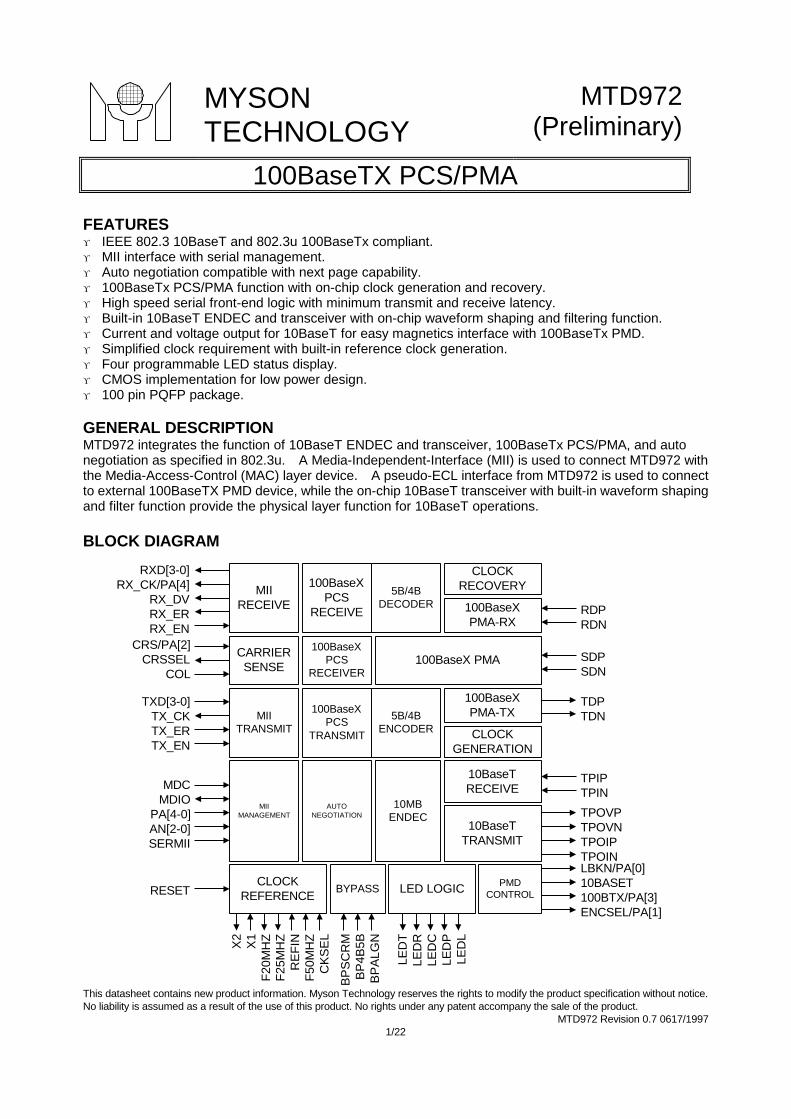
MYSON TECHNOLOGY MTD972 (Preliminary) 100BaseTX PCS/PMA This datasheet contains new product information. Myson Technology reserves the rights to modify the product specification without notice. No liability is assumed as a result of the use of this product. No rights under any patent accompany the sale of the product. MTD972 Revision 0.7 0617/1997 1/22 FEATURES ϒ IEEE 802.3 10BaseT and 802.3u 100BaseTx compliant. ϒ MII interface with serial management. ϒ Auto negotiation compatible with next page capability. ϒ 100BaseTx PCS/PMA function with on-chip clock generation and recovery. ϒ High speed serial front-end logic with minimum transmit and receive latency. ϒ Built-in 10BaseT ENDEC and transceiver with on-chip waveform shaping and filtering function. ϒ Current and voltage output for 10BaseT for easy magnetics interface with 100BaseTx PMD. ϒ Simplified clock requirement with built-in reference clock generation. ϒ Four programmable LED status display. ϒ CMOS implementation for low power design. ϒ 100 pin PQFP package. GENERAL DESCRIPTION MTD972 integrates the function of 10BaseT ENDEC and transceiver, 100BaseTx PCS/PMA, and auto negotiation as specified in 802.3u. A Media-Independent-Interface (MII) is used to connect MTD972 with the Media-Access-Control (MAC) layer device. A pseudo-ECL interface from MTD972 is used to connect to external 100BaseTX PMD device, while the on-chip 10BaseT transceiver with built-in waveform shaping and filter function provide the physical layer function for 10BaseT operations. BLOCK DIAGRAM MII RECEIVE 100BaseX PCS RECEIVE 5B/4B DECODER CLOCK RECOVERY 100BaseX PMA-RX CARRIER SENSE 100BaseX PCS RECEIVER 100BaseX PMA MII TRANSMIT 100BaseX PCS TRANSMIT 5B/4B ENCODER CLOCK GENERATION 100BaseX PMA-TX MII MANAGEMENT AUTO NEGOTIATION 10MB ENDEC 10BaseT RECEIVE 10BaseT TRANSMIT CLOCK REFERENCE BYPASS LED LOGIC PMD CONTROL RXD[3-0] RX_CK/PA[4] RX_DV RX_ER RX_EN CRS/PA[2] CRSSEL COL TXD[3-0] TX_CK TX_ER TX_EN MDC MDIO PA[4-0] AN[2-0] SERMII RESET RDP RDN SDP SDN TDP TDN TPIP TPIN TPOVP TPOVN TPOIP TPOIN LBKN/PA[0] 10BASET 100BTX/PA[3] ENCSEL/PA[1] X2 X1 F20MHZ F25MHZ REFIN F50MHZ CKSEL BPSCRM BP4B5B BPALGN LEDT LEDR LEDC LEDP LEDL
Transcript of MYSON TECHNOLOGY (Preliminary) · MYSON TECHNOLOGY MTD972 (Preliminary) 100BaseTX PCS/PMA This...
MYSONTECHNOLOGY
MTD972(Preliminary)
100BaseTX PCS/PMA
This datasheet contains new product information. Myson Technology reserves the rights to modify the product specification without notice.No liability is assumed as a result of the use of this product. No rights under any patent accompany the sale of the product.
MTD972 Revision 0.7 0617/19971/22
FEATURESϒ IEEE 802.3 10BaseT and 802.3u 100BaseTx compliant.ϒ MII interface with serial management.ϒ Auto negotiation compatible with next page capability.ϒ 100BaseTx PCS/PMA function with on-chip clock generation and recovery.ϒ High speed serial front-end logic with minimum transmit and receive latency.ϒ Built-in 10BaseT ENDEC and transceiver with on-chip waveform shaping and filtering function.ϒ Current and voltage output for 10BaseT for easy magnetics interface with 100BaseTx PMD.ϒ Simplified clock requirement with built-in reference clock generation.ϒ Four programmable LED status display.ϒ CMOS implementation for low power design.ϒ 100 pin PQFP package.
GENERAL DESCRIPTIONMTD972 integrates the function of 10BaseT ENDEC and transceiver, 100BaseTx PCS/PMA, and autonegotiation as specified in 802.3u. A Media-Independent-Interface (MII) is used to connect MTD972 withthe Media-Access-Control (MAC) layer device. A pseudo-ECL interface from MTD972 is used to connectto external 100BaseTX PMD device, while the on-chip 10BaseT transceiver with built-in waveform shapingand filter function provide the physical layer function for 10BaseT operations.
BLOCK DIAGRAM
MIIRECEIVE
100BaseXPCS
RECEIVE
5B/4BDECODER
CLOCKRECOVERY
100BaseXPMA-RX
CARRIERSENSE
100BaseXPCS
RECEIVER100BaseX PMA
MIITRANSMIT
100BaseXPCS
TRANSMIT
5B/4BENCODER CLOCK
GENERATION
100BaseXPMA-TX
MIIMANAGEMENT
AUTONEGOTIATION
10MBENDEC
10BaseTRECEIVE
10BaseTTRANSMIT
CLOCKREFERENCE BYPASS LED LOGIC PMD
CONTROL
RXD[3-0]RX_CK/PA[4]
RX_DVRX_ERRX_EN
CRS/PA[2]CRSSEL
COL
TXD[3-0]TX_CKTX_ERTX_EN
MDCMDIO
PA[4-0]AN[2-0]SERMII
RESET
RDPRDN
SDPSDN
TDPTDN
TPIPTPIN
TPOVPTPOVNTPOIPTPOINLBKN/PA[0]10BASET100BTX/PA[3]ENCSEL/PA[1]
X2
X1
F20M
HZ
F25M
HZ
RE
FIN
F50M
HZ
CK
SE
L
BP
SC
RM
BP
4B5B
BP
ALG
N
LED
TLE
DR
LED
CLE
DP
LED
L
MYSONTECHNOLOGY
MTD972(Preliminary)
MTD972 Revision 0.7 06/17/1997
2/22
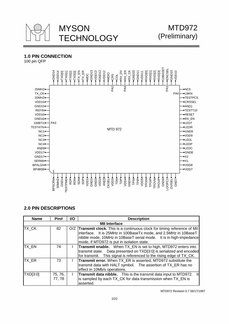
1.0 PIN CONNECTION100 pin QFP
MTD 972
BP
SC
RM
50M
HZ
GN
D1
TES
TPM
DR
DP
RD
NS
DN
SD
PV
DD
1G
ND
2G
ND
3V
DD
2A
N[2
]C
KS
EL
VD
D3
TDN
TDP
VD
D4
GN
D4
TPIN
TPIP
VD
D5
TPO
INTP
OIP
TPO
VN
TPO
VP
GN
D6
LOO
PC
1O
VIS
EL
GN
D7
GN
D14
VD
D14
TXD
[0]
TXD
[1]
TXD
[2]
TXD
[3]
TX_E
NTX
_ER
MD
CG
ND
13V
DD
13G
ND
12V
DD
12M
DIO
CR
SC
OL
RX
_DV
RX
_ER
RX
_CK
GN
D20
GN
D11
VD
D11
RX
D[0
]R
XD
[1]
RX
D[2
]R
XD
[3]
10B
AS
ET
EN
CS
EL
GN
D10
VD
D10
25MHZTX_CK20MHZVDD15GND15REFINVDD16GND16100BTX
TESTATNNC1NC2NC3NC4
AN[0]VDD17GND17SERMII
BPALGNBP4B5B
NC5LBKNTESTPCSCRSSELAN[1]TESTT10RESETRX_ENLEDTLEDRGND9VDD9LEDLLEDPLEDCGND8X2X1VDD8VDD7
PA
2
PA
4
PA
1
PA0
PA3
1
2.0 PIN DESCRIPTIONS
Name Pin# I/O DescriptionMII Interface
TX_CK 82 O/Z Transmit clock. This is a continuous clock for timing reference of MIIinterface. It is 25MHz in 100BaseTx mode, and 2.5MHz in 10BaseTnibble mode, 10MHz in 10BaseT serial mode. It is in high-impedancemode, if MTD972 is put in isolation state.
TX_EN 74 I Transmit enable. When TX_EN is set to high, MTD972 enters intotransmit state. Data presented on TXD[3:0] is serialized and encodedfor transmit. This signal is referenced to the rising edge of TX_CK.
TX_ER 73 I Transmit error. When TX_ER is asserted, MTD972 substitute thetransmit data with HALT symbol. The assertion of TX_ER has noeffect in 10Mb/s operations.
TXD[3:0] 75, 76,77, 78
I Transmit data nibble. This is the transmit data input to MTD972. Itis sampled by each TX_CK for data transmission when TX_EN isasserted.
MYSONTECHNOLOGY
MTD972(Preliminary)
MTD972 Revision 0.7 06/17/1997
3/22
Name Pin# I/O DescriptionRX_CK 62 O/Z Receive clock. MTD972 output a continuous clock stream on this
pin for receive timing reference. It is 25MHz in 100BaseTx mode,and 2.5MHz in 10Base nibble mode, 10MHz in 10Base serial mode.In 10BaseT mode, RX_CK is locked to the internal generated 20MHz,and transit to the recovered receive clock when receive is active.This output is high impedance state if RX_EN is not asserted orMTD972 is put in isolation state.
RX_DV 64 O/Z Receive data valid. This signal is used to encompass the validreceived packet. It is referenced to the rising edge of RX_CK. It is inhigh impedance if RX_EN is not asserted.
RX_ER 63 O/Z Receive error. This pin is asserted by MTD972 when an errorcondition occurs during reception of a packet in 100Mb/s operation.Specifically, this include "link fail", "bad SSD", and "data error" states.This pin is also used for RXD[5] in bypass modes. This pin has nomeaning in the 10Mb/s operation. This pin is put in high-impedancestate when RX_EN is not asserted.
RXD[3:0] 55, 56,57, 58
O/Z Receive data nibble. This is the receive data output from MTD972.It is referenced to the rising edge of RX_CK, and compassed byRX_DV. These pin is in high-impedance state when RX_EN is notasserted.
RX_EN 43 I Receive enable. This pin controls the output enable of RXD[3-0],RX_ER, RX_DV, and RX_CK but not CRS and COL. It has aninternal pull-up resistor.
CRS 66 O/Z Carrier sense. This pin is asserted when receive is active,configured in half-duplex mode. It is in high-impedance mode, whenMTD972 is in isolation state.
COL 65 O/Z Collision. This pin is used to indicate a collision condition whenMTD972 is in half-duplex mode. It also carries the SQE indication in10Mb/s operation. It is forced low if MTD972 is configured in full-duplex mode. It is in high-impedance mode, when MTD972 is inisolation state.
MDC 72 I Management data clock. This pin should be driven by themanagement station as the timing reference of MDIO.
MDIO 67 I/O Management data input/output. This is a bi-directional signalbetween MTD972 and the management station for exchange ofcontrol information and data. This pin has an internal pull-upresistor.
Auto NegotiationAutonegotiation enable/disable control. These pins define theauto-negotiation modes and capabilities of MTD972. Each input isbiased at an internal level if left unconnected. Thus three-state canbe differentiated: high, low, and floating. The capabilities andoperating modes are determined by the following table:
AN2 AN1 AN0 AutoNeg Capability0 0 0 ON 10Mb/s HDX0 0 1 ON 10Mb/s FDX0 1 0 ON 100Mb/s HDX
AN[2:0] 13, 46,95
I
0 1 1 ON 100Mb/s FDX
MYSONTECHNOLOGY
MTD972(Preliminary)
MTD972 Revision 0.7 06/17/1997
4/22
0 F F ON All capabilities
0 0 F OFF 10Mb/s HDX0 1 F OFF 10Mb/s FDX0 F 0 OFF 100Mb/s HDX0 F 1 OFF 100Mb/s FDX
1 0 0 ON 100Mb/s, 10Mb/s FDX1 0 1 ON 100Mb/s, 10Mb/s HDX1 1 0 ON 100Mb/s, FDX, HDX1 1 1 ON 10Mb/s, FDX, HDX
1 0 F OFF 100Mb/s, FDX, HDX1 F 0 OFF 100Mb/s, 10Mb/s FDX1 F 1 OFF 100Mb/s, 10Mb/s HDX
PCS/PMA ControlCRSSEL 47 I CRS function control. This pin select the function of CRS output.
When CRSSEL is high, CRS is asserted only when receive is activeregardless of either half or full duplex mode. This pin has an internalpull-down resistor.
SERMII 98 I Serial control. This pin select the interface method of MII data in10Mb/s mode. If SERMII is asserted a serial mode is enabled forinterfacing with a serial MAC device. Both TX_CK, RX_CK assume10MHz rate, and data is transferred using TXD[0] and RXD[0]. Whennot asserted, the transfer assumes MII compliant nibble mode. Thispin has no effect in 100Mb/s operation and has an internal pull-downresistor.
BPALGN 99 I Bypass alignment control. This pin is asserted to bypass the4B/5B coding/encoding, symbol alignment, and scrambling /descrambling process in the 100Mb/s operation. The transmit data in5 bit format (TX_ER:TXD[3:0]) is serialized and transmitted. Thereceived data also in 5 bit format (RX_ER:RXD[3:0]) is presented onthe MII interface. Both TX_CK and RX_CK are still 25MHz. Thispin has an internal pull-down resistor.
BP4B5B 100 I Bypass 4B/5B code/decode control. Similar to BPALGN, this pinis asserted to bypass the 4B/5B coding/encoding function of MTD972.The MII data interface assumes the 5 bit format. The symbolalignment and scrambling and descrambling function is still effective.This pin has an internal pull-down register.
BPSCRM 1 I Bypass scramble / descramble control. Similar to BPALGN, thispin is asserted to bypass the scrambling and descrambling function ofMTD972 in 100Mb/s operation. The MII data interface is in nibbleformat. This pin has an internal pull-down resistor.
Clock ReferenceCKSEL 14 I Clock reference mode select. This pin defines the operation
modes of reference clock generation and synthesis functions.CKSEL X1 X2 F25MHZ F20MHZF 1 0/F F50MHZ/2 SYN20MF 20M 20M F50MHZ/2 X1/X2 OSC
MYSONTECHNOLOGY
MTD972(Preliminary)
MTD972 Revision 0.7 06/17/1997
5/22
0 25M 25M X1/X2 OSC SYN20M1 25M 25M X1/X2 OSC SYN20M
If CKSEL=F, MTD972 output the divided by half signal from F50MHzto F25MHz for internal reference. If X1 is forced to hard high, than20MHz is synthesized. If X1 and X2 is connected to a 20MHz crystaloscillator, the oscillator output is used for internal reference.If CKSEL=1 or 0, MTD972 uses X1 and X2 on-chip oscillator for25MHz generation, and synthesize the internal 20MHz. In this case, a25MHz crystal should be connected between X1 and X2.
REFIN 86 I 25MHz reference clock in. All internal timing is derived from theclock input of this pin. A 25MHz continuous clock should beconnected to this pin. The clock source can be an external oscillator,or the output of F25MHZ.
F50MHZ 2 I 50MHz reference clock in. A 50MHz clock signal can be applied tothis pin to generate 25MHz clock at F25MHz output for internalreference. If not used, this pin should be pulled low. It has aninternal pull-down resistor.
X1 33 I Crystal oscillator. The output of on-chip crystal oscillator. It canbe used to generate either 25MHz or 20MHz clock depending on theCKSEL selection. If an external clock is used, it should be applied tothis pin. If it is forced high (to VDD or pull-up by a resistor less than4.7K), the oscillator is disabled, and internal synthesized clock is used.
X2 34 I Crystal oscillator. The input of on-chip crystal oscillator. If anexternal clock is used to applied at X1, X2 should be left open.
F25MHZ 81 O/Z 25MHz reference clock out. This pin output a 25MHz continuousclock from either divided by 2 of 50MHz input, or the 25MHz clock ofon-chip oscillator.
F20MHZ 83 O/Z 20MHz reference clock out. This pin output a 20MHz continuousclock from either the 20MHz on-chip oscillator, or the synthesized20MHz. This pin default in high-impedance mode after reset.
10BaseT PMDTPIP, TPIN 20, 21 I Differential twisted-pair receive input. A differential UTP receive
signal for 10Mb/s is input from these two pins. The inputs areinternally biased at 1/2 Vdd.
TPOVP,TPOVN
25, 26 O Differential voltage mode twisted-pair transmit output. Thesetwo pins provide a voltage mode output for 10Mb/s UTP transmit data.A serial termination resistor of 10.5Ohm should be connected betweeneach pin to the transformer. The isolation transformer should haveturn ratio of 1:2. The idle voltage on these two pins are at 2/3 Vdd.
TPOIP,TPOIN
23, 24 O Differential current mode twisted-pair transmit output. Thesetwo pins provide a current source mode output for 10Mb/s UTPtransmit data. Each pin should have a 50 Ohm termination resistorconnected to Vdd while connecting to the isolation transformer. Thetransformer should have turn ration of 1:1 with center-tap in theprimary side connected to Vdd.
OVISEL 29 I Output voltage/current mode select. This pin controls the power-on default setting of 10BaseT PMD output mode. If this pin is low,the voltage output, TPOVP, and TPOVN are enabled. If this pin ispulled high, TPOIP and TPOIN, current mode output is enabled.
MYSONTECHNOLOGY
MTD972(Preliminary)
MTD972 Revision 0.7 06/17/1997
6/22
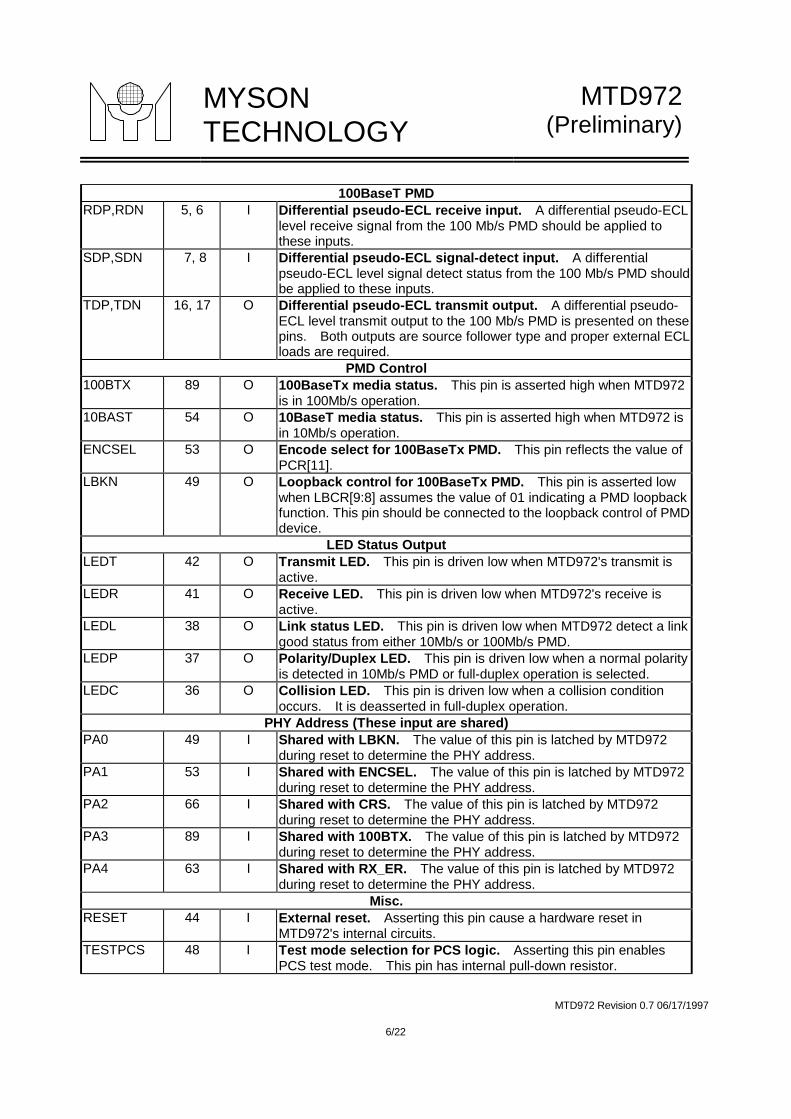
100BaseT PMDRDP,RDN 5, 6 I Differential pseudo-ECL receive input. A differential pseudo-ECL
level receive signal from the 100 Mb/s PMD should be applied tothese inputs.
SDP,SDN 7, 8 I Differential pseudo-ECL signal-detect input. A differentialpseudo-ECL level signal detect status from the 100 Mb/s PMD shouldbe applied to these inputs.
TDP,TDN 16, 17 O Differential pseudo-ECL transmit output. A differential pseudo-ECL level transmit output to the 100 Mb/s PMD is presented on thesepins. Both outputs are source follower type and proper external ECLloads are required.
PMD Control100BTX 89 O 100BaseTx media status. This pin is asserted high when MTD972
is in 100Mb/s operation.10BAST 54 O 10BaseT media status. This pin is asserted high when MTD972 is
in 10Mb/s operation.ENCSEL 53 O Encode select for 100BaseTx PMD. This pin reflects the value of
PCR[11].LBKN 49 O Loopback control for 100BaseTx PMD. This pin is asserted low
when LBCR[9:8] assumes the value of 01 indicating a PMD loopbackfunction. This pin should be connected to the loopback control of PMDdevice.
LED Status OutputLEDT 42 O Transmit LED. This pin is driven low when MTD972's transmit is
active.LEDR 41 O Receive LED. This pin is driven low when MTD972's receive is
active.LEDL 38 O Link status LED. This pin is driven low when MTD972 detect a link
good status from either 10Mb/s or 100Mb/s PMD.LEDP 37 O Polarity/Duplex LED. This pin is driven low when a normal polarity
is detected in 10Mb/s PMD or full-duplex operation is selected.LEDC 36 O Collision LED. This pin is driven low when a collision condition
occurs. It is deasserted in full-duplex operation.PHY Address (These input are shared)
PA0 49 I Shared with LBKN. The value of this pin is latched by MTD972during reset to determine the PHY address.
PA1 53 I Shared with ENCSEL. The value of this pin is latched by MTD972during reset to determine the PHY address.
PA2 66 I Shared with CRS. The value of this pin is latched by MTD972during reset to determine the PHY address.
PA3 89 I Shared with 100BTX. The value of this pin is latched by MTD972during reset to determine the PHY address.
PA4 63 I Shared with RX_ER. The value of this pin is latched by MTD972during reset to determine the PHY address.
Misc.RESET 44 I External reset. Asserting this pin cause a hardware reset in
MTD972's internal circuits.TESTPCS 48 I Test mode selection for PCS logic. Asserting this pin enables
PCS test mode. This pin has internal pull-down resistor.
MYSONTECHNOLOGY
MTD972(Preliminary)
MTD972 Revision 0.7 06/17/1997
7/22
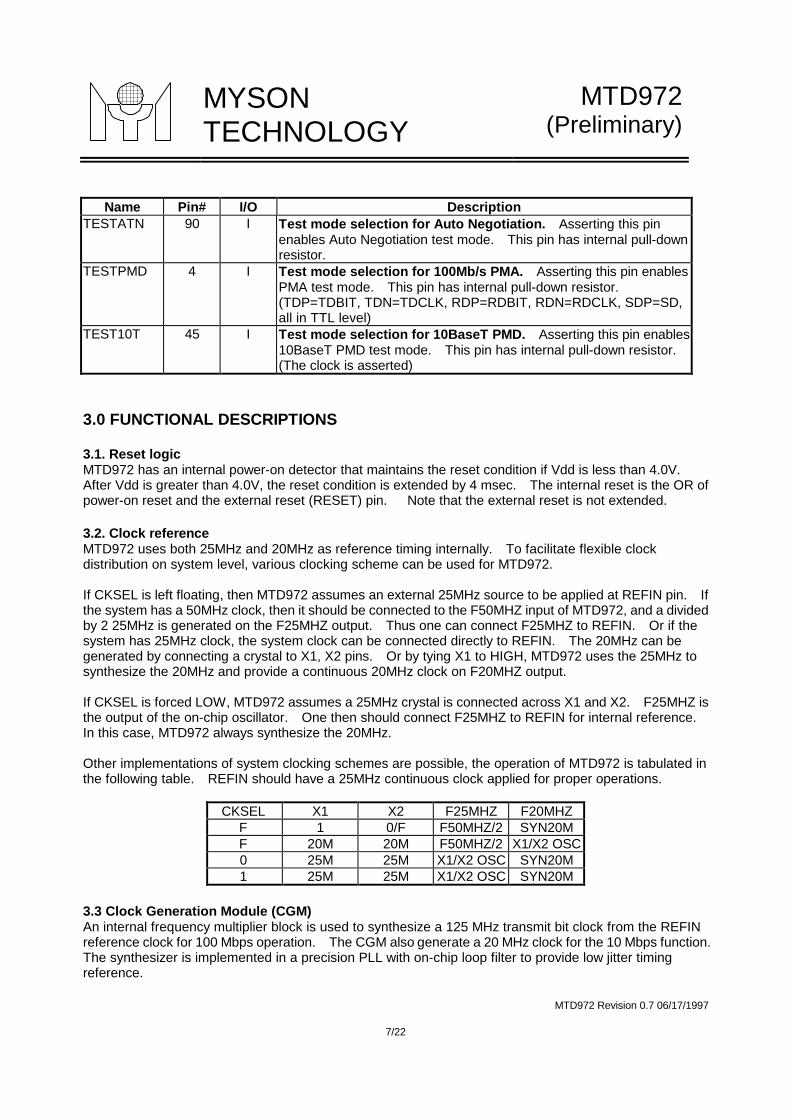
Name Pin# I/O DescriptionTESTATN 90 I Test mode selection for Auto Negotiation. Asserting this pin
enables Auto Negotiation test mode. This pin has internal pull-downresistor.
TESTPMD 4 I Test mode selection for 100Mb/s PMA. Asserting this pin enablesPMA test mode. This pin has internal pull-down resistor.(TDP=TDBIT, TDN=TDCLK, RDP=RDBIT, RDN=RDCLK, SDP=SD,all in TTL level)
TEST10T 45 I Test mode selection for 10BaseT PMD. Asserting this pin enables10BaseT PMD test mode. This pin has internal pull-down resistor.(The clock is asserted)
3.0 FUNCTIONAL DESCRIPTIONS
3.1. Reset logicMTD972 has an internal power-on detector that maintains the reset condition if Vdd is less than 4.0V.After Vdd is greater than 4.0V, the reset condition is extended by 4 msec. The internal reset is the OR ofpower-on reset and the external reset (RESET) pin. Note that the external reset is not extended.
3.2. Clock referenceMTD972 uses both 25MHz and 20MHz as reference timing internally. To facilitate flexible clockdistribution on system level, various clocking scheme can be used for MTD972.
If CKSEL is left floating, then MTD972 assumes an external 25MHz source to be applied at REFIN pin. Ifthe system has a 50MHz clock, then it should be connected to the F50MHZ input of MTD972, and a dividedby 2 25MHz is generated on the F25MHZ output. Thus one can connect F25MHZ to REFIN. Or if thesystem has 25MHz clock, the system clock can be connected directly to REFIN. The 20MHz can begenerated by connecting a crystal to X1, X2 pins. Or by tying X1 to HIGH, MTD972 uses the 25MHz tosynthesize the 20MHz and provide a continuous 20MHz clock on F20MHZ output.
If CKSEL is forced LOW, MTD972 assumes a 25MHz crystal is connected across X1 and X2. F25MHZ isthe output of the on-chip oscillator. One then should connect F25MHZ to REFIN for internal reference.In this case, MTD972 always synthesize the 20MHz.
Other implementations of system clocking schemes are possible, the operation of MTD972 is tabulated inthe following table. REFIN should have a 25MHz continuous clock applied for proper operations.
CKSEL X1 X2 F25MHZ F20MHZF 1 0/F F50MHZ/2 SYN20MF 20M 20M F50MHZ/2 X1/X2 OSC0 25M 25M X1/X2 OSC SYN20M1 25M 25M X1/X2 OSC SYN20M
3.3 Clock Generation Module (CGM)An internal frequency multiplier block is used to synthesize a 125 MHz transmit bit clock from the REFINreference clock for 100 Mbps operation. The CGM also generate a 20 MHz clock for the 10 Mbps function.The synthesizer is implemented in a precision PLL with on-chip loop filter to provide low jitter timingreference.
MYSONTECHNOLOGY
MTD972(Preliminary)
MTD972 Revision 0.7 06/17/1997
8/22
CGM also include the function of 100Mbps transmit. The serial transmit data in NRZI format is sampledby the transmit bit clock. A differential pseudo-ECL driver is used to drive TDP and TDN output pins.
3.4 Clock Recovery Module (CRM)The CRM is used to provide an accurate synchronization for the 100 Mbps received data. A reference125 MHz clock from CGM is used for a timing reference in the CRM. The synchronization to the incomingdata stream is achieved by aligning the delay of the reference clock to the data edge.
CRM also include the function of data slicing. Data sampling is achieved by a fast data comparator withthe synchronized received bit clock.
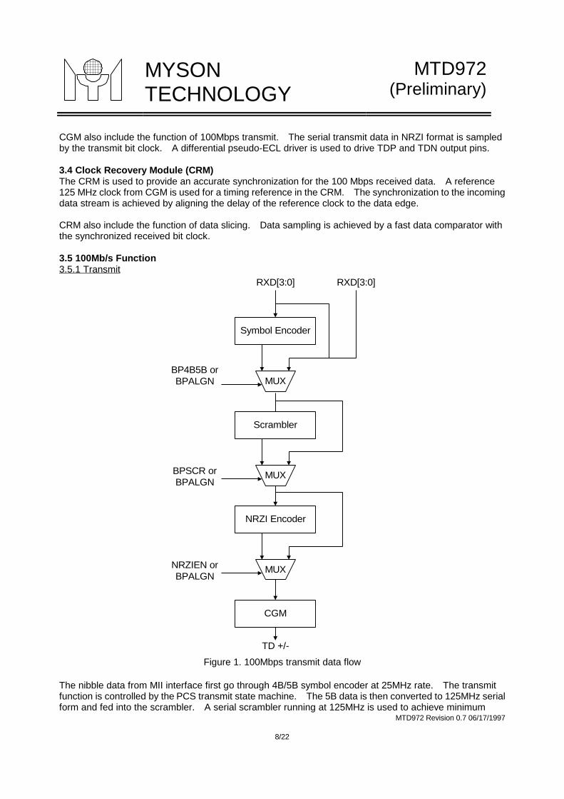
3.5 100Mb/s Function3.5.1 Transmit
Symbol Encoder
MUX
RXD[3:0] RXD[3:0]
BP4B5B orBPALGN
Scrambler
MUXBPSCR orBPALGN
NRZI Encoder
MUXNRZIEN orBPALGN
CGM
TD +/-
Figure 1. 100Mbps transmit data flow
The nibble data from MII interface first go through 4B/5B symbol encoder at 25MHz rate. The transmitfunction is controlled by the PCS transmit state machine. The 5B data is then converted to 125MHz serialform and fed into the scrambler. A serial scrambler running at 125MHz is used to achieve minimum
MYSONTECHNOLOGY
MTD972(Preliminary)
MTD972 Revision 0.7 06/17/1997
9/22
transmit latency. The output of the scrambler is then converted to NRZI format at the PMA-TX functionalblock. 100Base-X transmitter consists of function blocks, which convert synchronous 4B data to 5B data,scramble 5B data, and change it to be 125Mb/s serial data stream.
1. Symbol EncoderThe symbol encoder converts 4B nibble data to 5B symbol. This conversion allow control symbol to betransmitting along with data stream. At the beginning of the packet, the encoder will replace the first byteof preamble with J/K symbol denote the beginning of a packet. And add T/R at the end. Between thegap of two packet, add idle symbol.
2. ScramblerThe scramble is used to suppers the radiated emissions at the connector and twisted pair. The scrambleruse 11 bits LFSR to combine 5B code via XOR gate.
3. NRZI encoderEncode NRZ to NRZI for 802.3u specification.
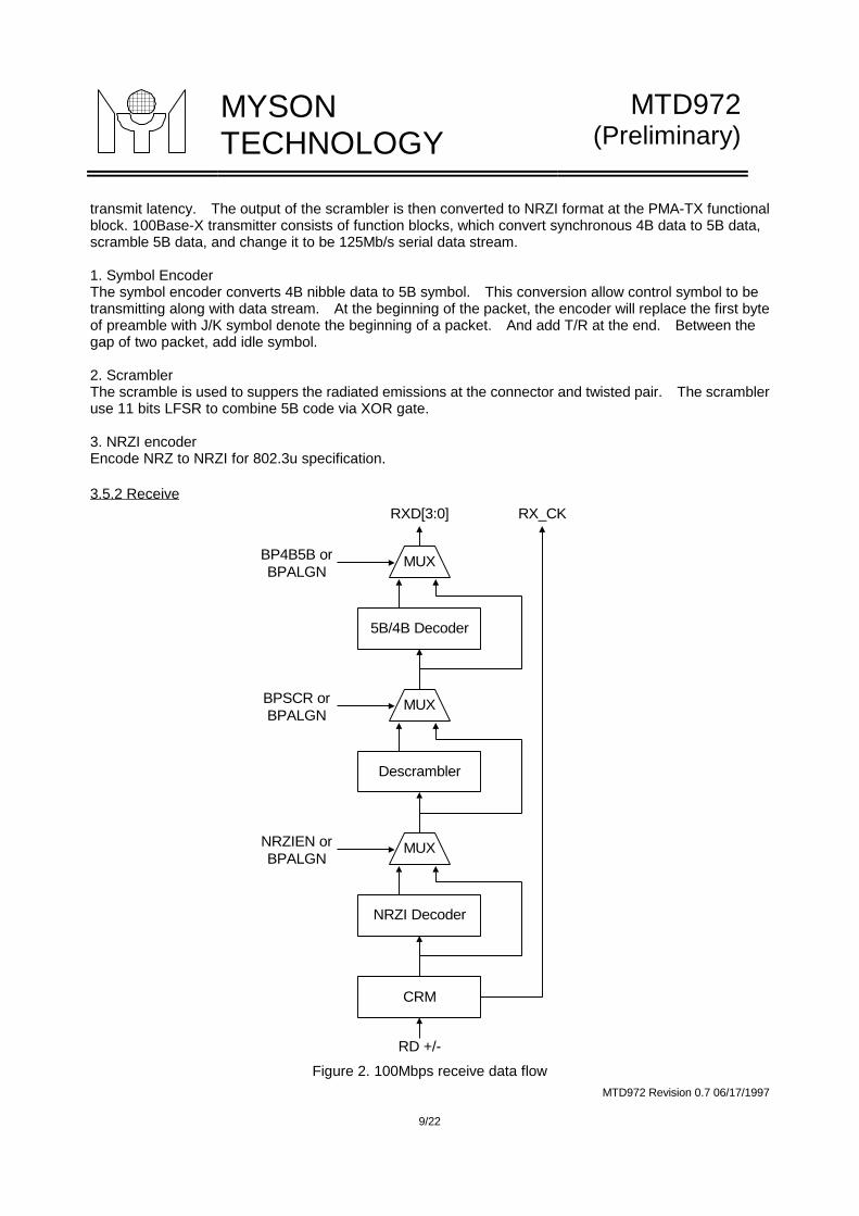
3.5.2 ReceiveRXD[3:0] RX_CK
5B/4B Decoder
BP4B5B orBPALGN
MUX
MUXBPSCR orBPALGN
Descrambler
MUXNRZIEN orBPALGN
NRZI Decoder
CRM
RD +/-
Figure 2. 100Mbps receive data flow
MYSONTECHNOLOGY
MTD972(Preliminary)
MTD972 Revision 0.7 06/17/1997
10/22
The serial received data from RDP and RDN pins are sampled by the CRM. The output of the receivefront end is first converted from NRZI format to NRZ format and then fed into a serial descrambler. Theuse of serial descrambler running at 125MHz ensures minimum receive latencyin the receive data path. Output of the descrambler is sent to the 5B/4B decoder controlled by the PCSreceive state machine. The 100Base-X receiver recover the data and clock from input data pair. Thendecode and align to be 4b nibble data.
1. NRZI decoderBefore descramble, must decode data to be NRZ format.
2. DescramblerTo descramble input data, the descrambler must generate identical key to recover the original data. Inorder to maintain the synchronization of the key, the descrambler monitor the descrambled data for each722 us. If there is not sufficient idle pattern, it will do synchronize again.
3. Symbol decoderAfter detect the start pattern "J/K", the symbol alignment will begin, and will change the phase of RX_CK.The symbol decoder acts as a look up table convert 5B code to 4B data.
3.5.3 Carrier Sense and CollisionThe carrier sense condition is asserted when either transmit and receive is active in half duplex mode.For full-duplex mode, only receive activity will assert the carrier sense signal. The collision condition isasserted if both transmit and receive are active in half-duplex mode. In full-duplex mode, the collision isalways deasserted.
3.5.4 Link StatusThe link monitor has a redundant carrier detect function. The link status is determined by the SD input.The link is asserted after a preset time of SD assertion according to the link monitor state diagram of 802.324.3.4.4.
The link function also include Far-End-Fault detect and generation. These functions can be optionallyenabled or disabled by the control register.
3.6 10Mbps Function3.6.1 TransmitThe transmit data from MII can take either nibble or serial format. An internal 20MHz reference clock isused to clock the Manchester encoder. The encoded data is sent to the UTP output driver.
Two set of output are available in MTD972. TPOIP and TPOIN are differential current-mode output withbuilt-in waveform shaping function. This output pair can be connected directly to the output of 100MHzPMD device. A 50 Ohm resistor connected to each pin and +5V should be usedas a common load among the 10Mbps and 100Mbps PMD. In addition, a 1CT:1 transformer with center-tap connected to +5V should be used for coupling to UTP media.
TPOVP and TPOVN are differential voltage-mode output also with built-in waveform shaping function.The output is a voltage source with very low output impedance, thus requires a series resistor to connectedto the transformer for media coupling. A 1:2 transformer and 12.5 Ohm resistors should be used.
3.6.2 ReceiveTPIP and TPIN is the receive differential pair for 10Mbps. These two pins are internally biased. Thedifferential signal need to meet both AC and DC squelch condition to enable the receive data path. The
MYSONTECHNOLOGY
MTD972(Preliminary)
MTD972 Revision 0.7 06/17/1997
11/22
received signal is connected to link test circuit to determine link status.
An on-chip PLL is used for Manchester decoding. The PLL is locked to an internally generated 10MHzclock and acquire fast phase synchronization to the incoming data edge of the preamble of the packet.Decoded data is then formatted to nibble width and passed to MII interface.
3.7 Auto-negotiationMTD972 implements auto-negotiation logic conforming to the 802.3u specification. The basic operationis based on using FLP to communicate information between link partners. The auto-negotiation takesthree phases to complete: advertising, detection and selection.
The auto-negotiation mode can be optionally selected using external pin selection AN[0-2]. MTD972 alsoimplement parallel detect function to allow compatibility with legacy network devices. Next page functionis also supported by MTD972 that allows exchange of arbitrary information between link partners, and bothmessage pages and unformatted page format are supported.
3.8 MII Serial Management and Register AccessThe MTD972 implement a set of control and status registers which MII specification required, and a subsetof option register. The access method is described below.
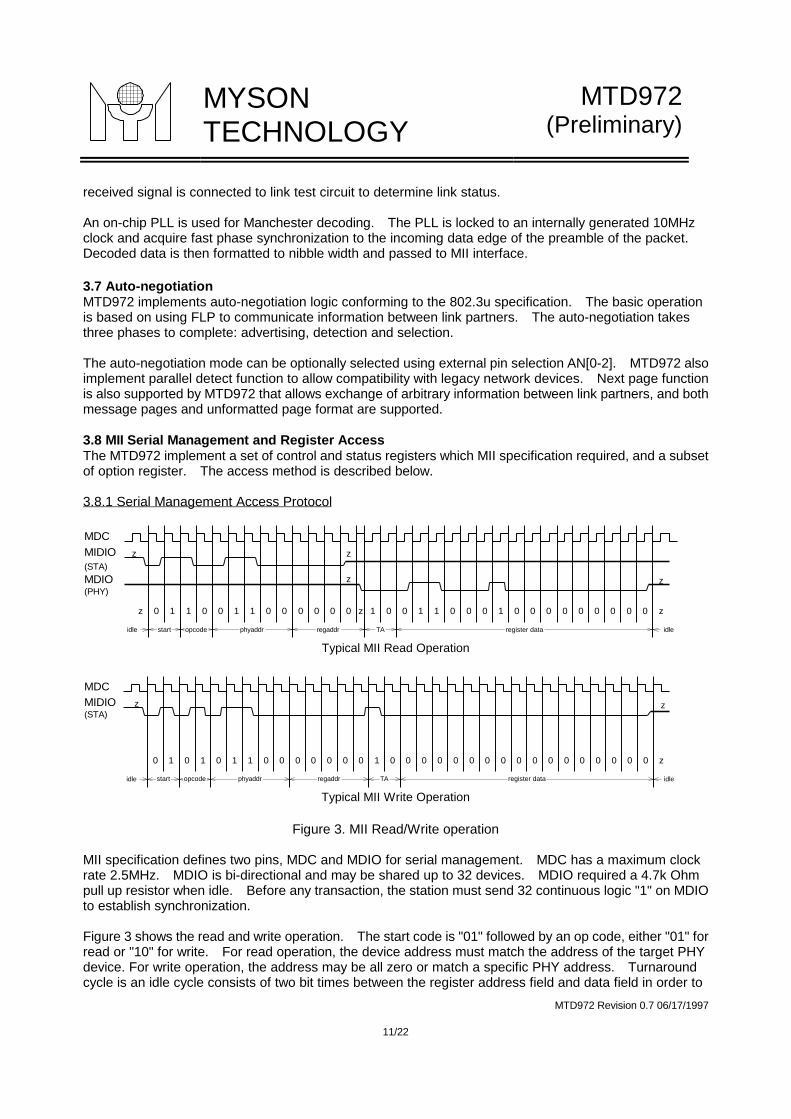
3.8.1 Serial Management Access Protocol
Typical MII Read Operation
Typical MII Write Operation
Figure 3. MII Read/Write operation
MII specification defines two pins, MDC and MDIO for serial management. MDC has a maximum clockrate 2.5MHz. MDIO is bi-directional and may be shared up to 32 devices. MDIO required a 4.7k Ohmpull up resistor when idle. Before any transaction, the station must send 32 continuous logic "1" on MDIOto establish synchronization.
Figure 3 shows the read and write operation. The start code is "01" followed by an op code, either "01" forread or "10" for write. For read operation, the device address must match the address of the target PHYdevice. For write operation, the address may be all zero or match a specific PHY address. Turnaroundcycle is an idle cycle consists of two bit times between the register address field and data field in order to
0 1 1 0 0 1 1 0 0 0 0 0 0 z 1 0 0 1 1 0 0 0 1 0 0 0 0 0 0 0 0 0
start opcode phyaddr regaddr TA register dataidle
z z
z
MDCMIDIO(STA)MDIO(PHY)
zz
idle
z
0 1 0 1 0 1 1 0 0 0 0 0
start opcode phyaddr regaddridle
0 1 0 0 0 0 0 0 0 0 0 0
TA register data
0 0 0 0 0 0 0 0
z
MDCMIDIO(STA)
z
z
idle
MYSONTECHNOLOGY
MTD972(Preliminary)
MTD972 Revision 0.7 06/17/1997
12/22
avoid conflict. For reading, no device drive MDIO in the first bit time, PHY drive "0" in the second bit time.For writing, station drive "10" during the idle cycle. Note that MTD972 always read and write at thepositive edge of MDC, so for read operation, the station must latch MDIO at the negative falling edge ofMDC.
3.8.2 PHY addressMTD972 uses 5 bits as PHY address, so there are 32 possible PHY address. The address is latched intointernal register during reset from the pin setting. If MTD972 latches an address "00000", it is put intoisolation mode. For an MII operation with address field "00000", the operation is treated as broadcast.
4.0 REGISTER DESCRIPTIONS
4.1 Control Register (CR 00H)00.15 RST Reset
Setting this bit causes a software reset operation in the PCS portion of the logic.RW/SC 0
00.14 LBK100 Loop Back Enable for the 100TX PHYLoopback the transmit data to the receive data. MTD972 exercises the loopback at the mostextensive way. The serialized transmit bit stream at 125MHz is looped back to the receivedCRM.Setting this bit high also asserts the internal signal_status and restart the synchronizationprocess of the descrambler. MTD972 should be isolated from the media in this loopbackmode.RW 0
00.13 SPD Speed SelectIf ANE is 0, then this bit select the link speed.If ANE is 1, this bit is ignored.1=100Mb/s, 0=10Mb/sRW 1
00.12 ANE Auto-Negotiation EnableSet to 1 to enable Auto-Negotiation operationRW 1
00.11 PWD Power-DownSet to 1 for power down operation.RW 0* This has no effect in MTD972. No power down mode is implemented in MTD972.
00.10 ISO IsolateSetting this bit will isolate the MTD972 from the MII bus.Specifically, all outputs RX_CLK, RX_DV, RX_ER, RXD, COL, CRS, TX_CLK are tri-state, andinputs TX_EN, TX_ER, TXD are ignored. The management port of MII is still active.RW 0
00.9 ANR Auto-Negotiation RestartSetting this bit cause the auto-negotiation process to be restarted. It is cleared when auto-negotiation process is finished. This bit has no effect if ANE=0.
MYSONTECHNOLOGY
MTD972(Preliminary)
MTD972 Revision 0.7 06/17/1997
13/22
RW/SC 0
00.8 FDX Full DuplexSetting this bit high when ANE=0, select the full-duplex operation. If ANE=1, this bit report theduplex selection of auto-negotiation.RW 1* Note for ANE=1. This bit is the same as 01.14.
00.7 CLT Collision TestSetting this bit cause the COL signal to be asserted when TX_EN is asserted.RW, 0
4.2 Status Register (SR 01H)01.15 T4C 100BaseT4 capability
RO, P 0
01.14 TXF 100BaseTX Full-Duplex capabilityRO, P 1
01.13 TXH 100BaseTX Half-Duplex capabilityRO, P 1
01.12 TFC 10BaseT Full-Duplex capabilityRO, P 1
01.11 THC 10BaseT Half-Duplex capabilityRO, P 1
01.6 MFP MF Preamble SuppressionMTD972 does not support the management interface without preamble pattern.RO, P 0
01.5 ANC Auto-Negotiation CompleteThis bit reflects the status of auto-negotiation process.RO, SC 0* This bit is read 0 if ANE=0.
01.4 RFS Remote Fault statusThis bit is set to indicate a remote fault condition has been detected. This bit should be clearedevery time this register is accessed. It is also set if the link word received from the link partnerwith RF bit set (05.13).RO, L 0
01.3 ANA Auto-Negotiation AbilityMTD972 has this abilityRO, P 1
01.2 LNK Link StatusThis bit is set that if a vaild link is established either as 100TX or 10BaseT. The bit has alatching function that once it is reset to indicated link fail, it remains cleared until the register isaccessed.RO, L 0

MYSONTECHNOLOGY
MTD972(Preliminary)
MTD972 Revision 0.7 06/17/1997
14/22
01.1 JABThis bit is set that if a jabber condition is detected in 10BaseT operation. This has the samelatching feature as LNK bit.RO, L 0
01.0 EXT Extended CapabilityMTD972 support the extended register functionRO, P 1
4.3 PHY Identifier Register 1 (PIR1 02H)This register contains the OUI information.
4.4 PHY Identifier Register 2 (PIR1 03H)This register contains the OUI information.
4.5 Auto-Negotiation Advertisement Register (ANAR 04H)
04.15 NP Next Page IndicationThis bit should be set when the register contains the next page information. This bit should beset if local MTD972 want to engage the next-page exchange with its link partner. This bit alsorepresent the NP filed of transmitted base link code word.RW, 0
04.14 ACK AcknowledgeThis bit is controlled by MTD972 during the auto-negotiation process. Writing to this bit has noeffect. Reading this bit reflect the ACK bit status of auto-negotiation.RO, 0
04.13 RF Remote FaultThis bit is set by management to indicate that a remote fault condition is detected.RW, 0
04.9 T4 100BaseT4 capabilityMTD972 does not support 100BaseT4.RO, P 0
04.8 TXF 100BaseTx Full-duplex capabilityThis bit is set by the management.RW, 1
04.7 TXH 100BaseTx Half-duplex capabilityThis bit is set by the management.RW, 1
04.6 TBF 10BaseT Full-duplex capabilityThis bit is set by the management.RW, 1
04.5 TBH 10BaseT half-duplex capabilityThis bit is set by the management.RW, 1
MYSONTECHNOLOGY
MTD972(Preliminary)
MTD972 Revision 0.7 06/17/1997
15/22
04.4:0 SLF Selector FiledThis five bit should be set to identify the type of messagesent by auto-negotiation.00001: IEEE 802.300010: IEEE 802.9All other combination are reserved.RW, 00001
4.6 Auto-Negotiation Link Partner Ability Register (ANLPAR 05H)05.15 NP Next Page Indicate
This bit is set when the partner wish to engage in next page transfer.RO, 0
05.14 ACK AcknowledgeThis bit is the ACK bit received from the link partner. It is set by the link partner when itacknowledge the reception of the link code word.RO, 0
05.13 RF Remote FaultThis bit is the RF bit received from the link partner. It is set by the link partner when it detect aremote fault condition. This bit also control the RFS bit in basic status register.RO, 0
05.9 T4 100BaseT4 capabilityThis bit is set by link partner when it support 100BaseT4.RO, 0
05.8 TXF 100BaseTx Full-duplex capabilityThis bit is set by link partner when it support 100BaseTX full duplex.RO, 0
05.7 TXH 100BaseTx Half-duplex capabilityThis bit is set by link partner when it support 100BaseTX half duplex.RO, 1
05.6 TBF 10BaseT Full-duplex capabilityThis bit is set by link partner when it support 10BaseT full duplex.RO, O
05.5 TBH 10BaseT half-duplex capabilityThis bit is set by link partner when it support 10BaseT half duplex.RO, 0
05.4:0 SLF Selector FiledThis is the bit received from the link partner indicating the protocol selection.00001: IEEE 802.300010: IEEE 802.9All other combination is reserved.RO, 00000
*This register is also used to receive the next page information. In this case the meaning of this register isredefined as following
MYSONTECHNOLOGY
MTD972(Preliminary)
MTD972 Revision 0.7 06/17/1997
16/22
05.15 NP Next Page IndicateThis bit is set when the partner has additional next page to transmit.
05.14 ACK AcknowledgeThis bit is the ACK bit received.
05.13 MPG Message PageThis bit is set if a coded message.
05.12 ACK2 Acknowledge 2This bit is set by the link partner if it will comply with the received message.
05.11 TGL ToggleThis bit is used to maintain synchronization of the next page transfer.
05.10:0 DAT DataData can either be a coded message or unformatted page.
4.7 Auto-Negotiation Expansion Register (ANER 06H)06.4 PDF Parallel Detection Fault
This bit is set by the auto-negotiation process if a parallel detection fault has occurred. That isnone or more than one of the NLP, 100BaseTX have indicated link ready. This bit has alatching function and is cleared by accessing this register.RO,L0
06.3 LPNPA Link Partner Next Page AbilityThis bit is set when received base link code work from the link partner has its NP bit set.RO, 0
06.2 NPA Next Page AbilityMTD972 support the next page function. This bit is used to control the autonegotiation arbiterstate machine.RO,P 1
06.1 RCV Page ReceivedThis bit is set to indicate that a new link code word is received and stored in ANLPAR. This bitis cleared when ANLPAR is read.RO,L0
06.0 LPANA Link Partner Auto-Negotiation AbilityThis bit is set if MTD972 detect that its link partner support auto negotiation.RO, 0
4.8 Auto-Negotiation Next Page Transmit Register (ANNPTR 07H)07.15 NP Next Page
This bit is set to indicate that additional pages is to be transmitted.RW, 0
07.14 ACK AcknowledgeThis bit is controlled by the auto-negotiation process of MTD972.RO, 0
MYSONTECHNOLOGY
MTD972(Preliminary)
MTD972 Revision 0.7 06/17/1997
17/22
07.13 MPG Message PageThis bit is set to indicate the data contained is a coded message.RW, 1
07.12 ACK2 Acknowledge 2This bit is set to indicate that local device is able to comply the coded message just received.RW, 0
07.11 TGL ToggleThis bit is controlled by the auto-negotiation process of MTD972.RO, 0
07.10:0 DAT DataThis is a 11 bit data field contains either coded message or unformatted information.
4.9 Disconnect Counter Register (DCR 12H) This register contains the partition count
4.10 False Carrier Sense Counter Register (FCSCR 13H)This counter is incremented when a false carrier sense condition is detected. A false carriersense condition is meant that a frame is not started with /J/K/ symbol.RO, SC 0000H
4.11 Receive Error Counter Register (RECR 15H)This counter is incremented when a receive error condition is detected. A receive error includethe DATA ERROR, PREMATURE END during valid packet reception.RO, SC 0000H
4.12 Revision Register (RR 16H)This register contains the revision number of MTD972.RO, P 0000H
4.13 PHY Configuration Register (PCR 17H)17.15 NRZIEN NRZI Encoding/Decoding
This bit controls the NRZI encoding and decoding function.If cleared, the NRZI encoding and decoding function is bypassed.RW, 1
17.14 TOSEL Descrambler Time Out SelectThis bit is set to 1 to select Time out time as 2000us.If it is 0, then the time out is 722us.RW, 0
17.13 TODIS Descrambler Time Out DisableThis bit is set to disable the time out counter in the descrambler.RW, 0
17.12 RPTR RepeaterThis bit should be set for repeater application. In this case, CRS output only reflect the receiveactivity.RW, CRSSEL
MYSONTECHNOLOGY
MTD972(Preliminary)
MTD972 Revision 0.7 06/17/1997
18/22
17.11 ENCSEL PMD ENCSEL controlThis bit is used to control the output on ENCSEL pin.RW, 0
17.8 20MENB 20MHZ output enableThis bit is set to enable the 20MHz output. Default is disable.RW, 0
17.7 25MDIS 25MHZ output disableThis bit is set to tristate the 25MHz output. Default is enable.RW, 0
17.6 FGLNKTX Force good link in 100BaseTx modeIf this bit is cleared, the 100BaseTx PMA link status is forced to be in ready state.RW, 1
17.5 FCONNT Bypass the Disconnect functionThis bit is set to bypass the disconnect function.RW, 0
17.4 TXOFF Transmit OffThis bit is set to turn off the 100BaseTx output in an idle state.RW, 0
17.2 LEDTSL LEDT display function selectIf this bit is set to 1, then LEDT indicates the status of disconnect function.RW, 0
17.1 LEDPSL LEDP display function selectIf this bit is set to 1, then LEDP indicates the full duplex operation of 10BaseT.If this bit is set to 0, then LEDP indicates the polarity of 10Mb/s, or the FDX in 100Mb/s.
4.14 Loopback and Bypass Control Register (LBCR 18H)
18.14 BP4B5B
18.13 BPSCRM
18.12 BPALGN Bypass Symbol Alignment
18.11 LBK10 Loopback control for 10BaseTThis bit is set to perform loopback test in 10BaseT section.RW, 0
18.9 LBK1 Loopback control 1 for PMDRW, 0
18.8 LBK0 Loopback control 0 for PMDRW, 0
MYSONTECHNOLOGY
MTD972(Preliminary)
MTD972 Revision 0.7 06/17/1997
19/22
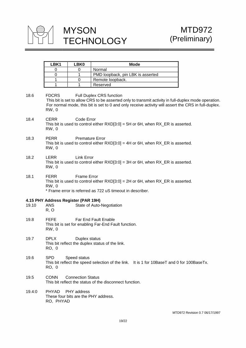
LBK1 LBK0 Mode0 0 Normal0 1 PMD loopback, pin LBK is asserted1 0 Remote loopback.1 1 Reserved
18.6 FDCRS Full Duplex CRS functionThis bit is set to allow CRS to be asserted only to transmit activity in full-duplex mode operation.For normal mode, this bit is set to 0 and only receive activity will assert the CRS in full-duplex.RW, 0
18.4 CERR Code ErrorThis bit is used to control either RXD[3:0] = 5H or 6H, when RX_ER is asserted.RW, 0
18.3 PERR Premature ErrorThis bit is used to control either RXD[3:0] = 4H or 6H, when RX_ER is asserted.RW, 0
18.2 LERR Link ErrorThis bit is used to control either RXD[3:0] = 3H or 6H, when RX_ER is asserted.RW, 0
18.1 FERR Frame ErrorThis bit is used to control either RXD[3:0] = 2H or 6H, when RX_ER is asserted.RW, 0* Frame error is referred as 722 uS timeout in describer.
4.15 PHY Address Register (PAR 19H)19.10 ANS State of Auto-Negotiation
R, O
19.8 FEFE Far End Fault EnableThis bit is set for enabling Far-End Fault function.RW, 0
19.7 DPLX Duplex statusThis bit reflect the duplex status of the link.RO, 0
19.6 SPD Speed statusThis bit reflect the speed selection of the link. It is 1 for 10BaseT and 0 for 100BaseTx.RO, 0
19.5 CONN Connection StatusThis bit reflect the status of the disconnect function.
19.4:0 PHYAD PHY addressThese four bits are the PHY address.RO, PHYAD
MYSONTECHNOLOGY
MTD972(Preliminary)
MTD972 Revision 0.7 06/17/1997
20/22
4.16 10Base-T Status Register (10SR 1BH)1B.9 10BTSER Serial mode for 10BaseT interface
This bit controls the serial mode operation of 10BaseT
RW, 10BTSER1B.0 POLST Polarity state
RO, 0
4.17 10Base-T Control Register (10CR 1CH)1C.5 LOE Link Pulse Output Enable
This bit controls the output of link pulse in 10BaseT mode. This bit does not affect the output ofFLP in Auto-Neg.RW, 1
1C.4 HBE Heartbeat EnableThis bit controls the Heartbeat function of 10BaseT PMD.RW, 1
1C.3 UTPV This bit controls the either TPOV or TPOI output. Set to1 for TPOV, and 0 for TPOIRW, 1
1C.2 LSS Low Squelch SelectThis bit has no effect.RW, 0
1C.1 PENB Polarity Enable ControlThis bit when set 0 enables the polarity correction of the 10BaseT transceiver.RW,0
1C.0 JEN Jabber EnableThis bit controls the Jabber function in the 10BaseT PMD.RW, 1
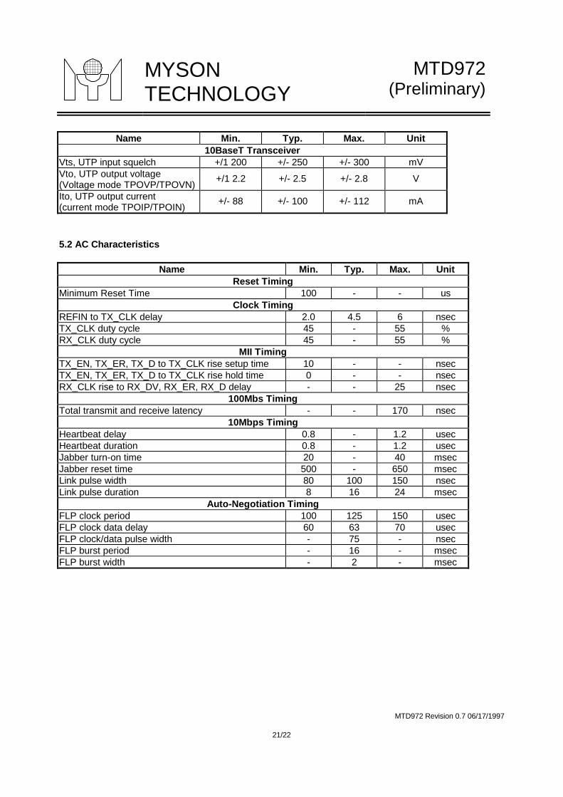
5.0 ELECTRICAL CHARACTERISTICS
5.1 DC Characteristics
Name Min. Typ. Max. UnitIdd - 150 220 mA
MII InterfaceVih, MII 2.0 - - VVil, MII - - 0.8 VVoh, MII 2.4 - - VVol, MII - - 0.4 V
PMD InterfaceVih, ECL Vdd-1.16 - Vdd-0.88 VVil, ECL Vdd-1.81 - Vdd-1.47 VVoh, ECL Vdd-1.00 - - VVol, ECL - - Vdd-1.62 V
MYSONTECHNOLOGY
MTD972(Preliminary)
MTD972 Revision 0.7 06/17/1997
21/22
Name Min. Typ. Max. Unit10BaseT Transceiver
Vts, UTP input squelch +/1 200 +/- 250 +/- 300 mVVto, UTP output voltage(Voltage mode TPOVP/TPOVN)
+/1 2.2 +/- 2.5 +/- 2.8 V
Ito, UTP output current(current mode TPOIP/TPOIN)
+/- 88 +/- 100 +/- 112 mA
5.2 AC Characteristics
Name Min. Typ. Max. UnitReset Timing
Minimum Reset Time 100 - - usClock Timing
REFIN to TX_CLK delay 2.0 4.5 6 nsecTX_CLK duty cycle 45 - 55 %RX_CLK duty cycle 45 - 55 %
MII TimingTX_EN, TX_ER, TX_D to TX_CLK rise setup time 10 - - nsecTX_EN, TX_ER, TX_D to TX_CLK rise hold time 0 - - nsecRX_CLK rise to RX_DV, RX_ER, RX_D delay - - 25 nsec
100Mbs TimingTotal transmit and receive latency - - 170 nsec
10Mbps TimingHeartbeat delay 0.8 - 1.2 usecHeartbeat duration 0.8 - 1.2 usecJabber turn-on time 20 - 40 msecJabber reset time 500 - 650 msecLink pulse width 80 100 150 nsecLink pulse duration 8 16 24 msec
Auto-Negotiation TimingFLP clock period 100 125 150 usecFLP clock data delay 60 63 70 usecFLP clock/data pulse width - 75 - nsecFLP burst period - 16 - msecFLP burst width - 2 - msec
MYSONTECHNOLOGY
MTD972(Preliminary)
MTD972 Revision 0.7 06/17/1997
22/22
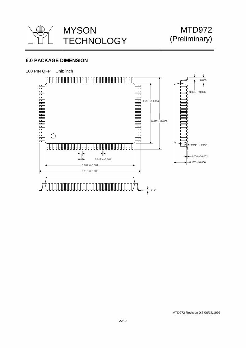
6.0 PACKAGE DIMENSION
100 PIN QFP Unit: inch
0.913 +/-0.008
0.787 +/-0.004
0.012 +/-0.0040.026
0.677 +/-0.008
0.551 +/-0.004
0.107 +/-0.006
0.014 +/-0.004
0.031 +/-0.006
0.063
0~70
0.006 +/-0.002