mul or mulu - renesas.com
45
Document No. ZBG-CC-09-0049 1/5 Date issued November 9, 2009 V850ES/Kx1 Microcontrollers Usage Restrictions Issued by Product Solution Group Multipurpose Microcomputer Systems Division Microcomputer Operations Unit NEC Electronics Corporation √ Usage restriction Upgrade Document modification Related documents: V850ES/KF1 Hardware User’s Manual: U16891EJ2V0UD00 (2nd edition) V850ES/KG1 Hardware User’s Manual: U16890EJ2V0UD00 (2nd edition) V850ES/KJ1 Hardware User’s Manual: U16889EJ2V0UD00 (2nd edition) V850ES Architecture User’s Manual: U15943EJ3V0UM00 (3rd edition) Notification classification Other notification 1. Affected products All V850ES/Kx1 microcontrollers (except for V850ES/KE1) V850ES/KF1: μPD703208, μPD703208Y, μPD703209, μPD703209Y, μPD703210, μPD703210Y, μPD70F3210, μPD70F3210Y, μPD70F3210H, μPD70F3210HY, μPD70F3211H, μPD70F3211HY V850ES/KG1: μPD703212, μPD703212Y, μPD703213, μPD703213Y, μPD703214, μPD703214Y, μPD70F3214, μPD70F3214Y, μPD70F3214H, μPD70F3214HY, μPD703215, μPD703215Y, μPD70F3215H, μPD70F3215HY V850ES/KJ1: μPD703216, μPD703216Y, μPD703217, μPD703217Y, μPD70F3217, μPD70F3217Y, μPD70F3217H, μPD70F3217HY, μPD70F3218H, μPD70F3218HY 2. Notification The following restriction for the V850ES/Kx1 microcontrollers has been found. Restriction No. 3: Restriction on executing a mul or mulu instruction (2) Description: The following occur if a specific instruction sequence (sequence 1 or 2 below) is executed. • The result of executing a multiplication instruction is not stored in the relevant general-purpose register. • As a result of executing an ld instruction for a mis-aligned address, the data at an incorrect address is read and stored in the relevant general-purpose register. Sequence 1: In the following instruction sequence, the RAM is read by one of the instructions in (2) at the same time as the RAM is accessed by a DMA transfer: (1) ld or sld: A load instruction for the internal ROM (2) ld or sld: A load instruction for the internal RAM (3) mul or mulu: An instruction that multiplies word data and whose result is truncated to 32 bits Note 1 ... Note 2 (4) ld or sld: A load instruction for a mis-aligned address in the internal ROM or RAM
Transcript of mul or mulu - renesas.com
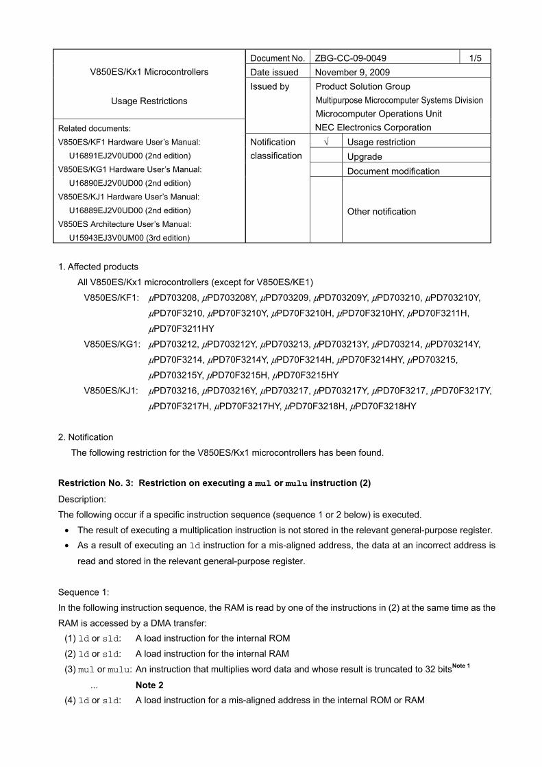
Document No. ZBG-CC-09-0049 1/5 Date issued November 9, 2009 V850ES/Kx1 Microcontrollers
Usage Restrictions
Issued by Product Solution Group Multipurpose Microcomputer Systems Division Microcomputer Operations Unit NEC Electronics Corporation
√ Usage restriction Upgrade
Document modification
Related documents:
V850ES/KF1 Hardware User’s Manual:
U16891EJ2V0UD00 (2nd edition)
V850ES/KG1 Hardware User’s Manual:
U16890EJ2V0UD00 (2nd edition)
V850ES/KJ1 Hardware User’s Manual:
U16889EJ2V0UD00 (2nd edition)
V850ES Architecture User’s Manual:
U15943EJ3V0UM00 (3rd edition)
Notification classification
Other notification
1. Affected products
All V850ES/Kx1 microcontrollers (except for V850ES/KE1)
V850ES/KF1: μPD703208, μPD703208Y, μPD703209, μPD703209Y, μPD703210, μPD703210Y,
μPD70F3210, μPD70F3210Y, μPD70F3210H, μPD70F3210HY, μPD70F3211H,
μPD70F3211HY
V850ES/KG1: μPD703212, μPD703212Y, μPD703213, μPD703213Y, μPD703214, μPD703214Y,
μPD70F3214, μPD70F3214Y, μPD70F3214H, μPD70F3214HY, μPD703215,
μPD703215Y, μPD70F3215H, μPD70F3215HY
V850ES/KJ1: μPD703216, μPD703216Y, μPD703217, μPD703217Y, μPD70F3217, μPD70F3217Y,
μPD70F3217H, μPD70F3217HY, μPD70F3218H, μPD70F3218HY
2. Notification
The following restriction for the V850ES/Kx1 microcontrollers has been found.
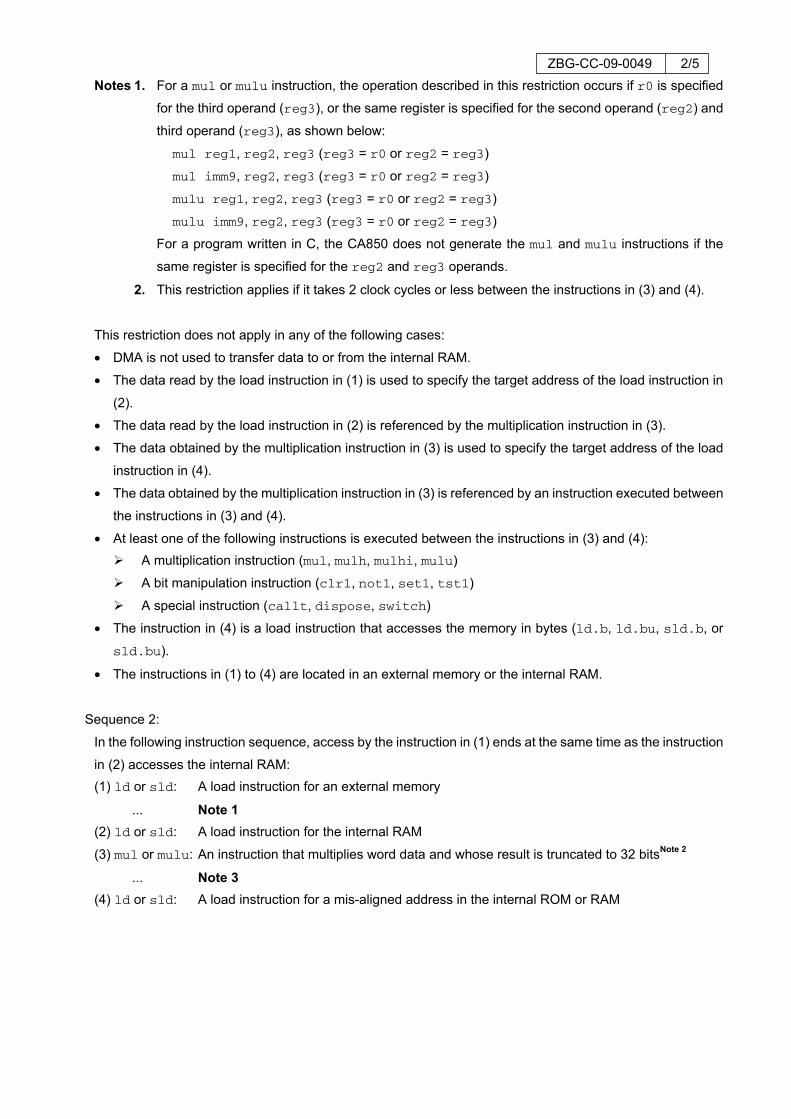
Restriction No. 3: Restriction on executing a mul or mulu instruction (2)
Description:
The following occur if a specific instruction sequence (sequence 1 or 2 below) is executed.
• The result of executing a multiplication instruction is not stored in the relevant general-purpose register. • As a result of executing an ld instruction for a mis-aligned address, the data at an incorrect address is
read and stored in the relevant general-purpose register.
Sequence 1:
In the following instruction sequence, the RAM is read by one of the instructions in (2) at the same time as the
RAM is accessed by a DMA transfer: (1) ld or sld: A load instruction for the internal ROM
(2) ld or sld: A load instruction for the internal RAM
(3) mul or mulu: An instruction that multiplies word data and whose result is truncated to 32 bitsNote 1
... Note 2 (4) ld or sld: A load instruction for a mis-aligned address in the internal ROM or RAM
ZBG-CC-09-0049 2/5 Notes 1. For a mul or mulu instruction, the operation described in this restriction occurs if r0 is specified
for the third operand (reg3), or the same register is specified for the second operand (reg2) and
third operand (reg3), as shown below:
mul reg1, reg2, reg3 (reg3 = r0 or reg2 = reg3)
mul imm9, reg2, reg3 (reg3 = r0 or reg2 = reg3)
mulu reg1, reg2, reg3 (reg3 = r0 or reg2 = reg3)
mulu imm9, reg2, reg3 (reg3 = r0 or reg2 = reg3)
For a program written in C, the CA850 does not generate the mul and mulu instructions if the
same register is specified for the reg2 and reg3 operands.
2. This restriction applies if it takes 2 clock cycles or less between the instructions in (3) and (4).
This restriction does not apply in any of the following cases:
• DMA is not used to transfer data to or from the internal RAM.
• The data read by the load instruction in (1) is used to specify the target address of the load instruction in
(2).
• The data read by the load instruction in (2) is referenced by the multiplication instruction in (3).
• The data obtained by the multiplication instruction in (3) is used to specify the target address of the load
instruction in (4).
• The data obtained by the multiplication instruction in (3) is referenced by an instruction executed between
the instructions in (3) and (4).
• At least one of the following instructions is executed between the instructions in (3) and (4): A multiplication instruction (mul, mulh, mulhi, mulu)
A bit manipulation instruction (clr1, not1, set1, tst1)
A special instruction (callt, dispose, switch)
• The instruction in (4) is a load instruction that accesses the memory in bytes (ld.b, ld.bu, sld.b, or
sld.bu).
• The instructions in (1) to (4) are located in an external memory or the internal RAM.
Sequence 2:
In the following instruction sequence, access by the instruction in (1) ends at the same time as the instruction
in (2) accesses the internal RAM: (1) ld or sld: A load instruction for an external memory
... Note 1 (2) ld or sld: A load instruction for the internal RAM
(3) mul or mulu: An instruction that multiplies word data and whose result is truncated to 32 bitsNote 2
... Note 3 (4) ld or sld: A load instruction for a mis-aligned address in the internal ROM or RAM
ZBG-CC-09-0049 3/5
Notes 1. This restriction applies if a different instruction is executed between the load instructions in (1) and
(2), and the access by the instruction in (1) ends at the same time as the instruction in (2)
accesses the internal RAM. 2. For a mul or mulu instruction, the operation described in this restriction occurs if r0 is specified
for the third operand (reg3), or the same register is specified for the second operand (reg2) and
third operand (reg3), as shown below: mul reg1, reg2, reg3 (reg3 = r0 or reg2 = reg3)
mul imm9, reg2, reg3 (reg3 = r0 or reg2 = reg3)
mulu reg1, reg2, reg3 (reg3 = r0 or reg2 = reg3)
mulu imm9, reg2, reg3 (reg3 = r0 or reg2 = reg3)
For a program written in C, the CA850 does not generate the mul and mulu instructions if the
same register is specified for the reg2 and reg3 operands.
3. This restriction applies if it takes 2 clock cycles or less between the instructions in (3) and (4).
This restriction does not apply in any of the following cases:
• An external bus is not used.
• The data read by the load instruction in (1) is used to specify the target address of the load instruction in
(2).
• The data read by the load instruction in (1) is referenced by an instruction executed between the
instructions in (1) and (2).
• The data read by the load instruction in (2) is referenced by the multiplication instruction in (3).
• The data obtained by the multiplication instruction in (3) is used to specify the target address of the load
instruction in (4).
• The data obtained by the multiplication instruction in (3) is referenced by an instruction executed between
the instructions in (3) and (4).
• At least one of the following instructions is executed between the instructions in (3) and (4): A multiplication instruction (mul, mulh, mulhi, mulu)
A bit manipulation instruction (clr1, not1, set1, tst1)
A special instruction (callt, dispose, switch)
• The instruction in (4) is a load instruction that accesses the memory in bytes (ld.b, ld.bu, sld.b, or
sld.bu).
• The instructions in (1) to (4) are located in an external memory or the internal RAM.
Workaround:
Action for systems being developed and to be developed in future:
We regard this as a restriction related to the CPU’s features and do not intend to correct the microcontroller.
Instead, the CA850 compiler will be modified to automatically prevent instructions to which this restriction
applies from being generated. This workaround does not work for instructions in assembly code, so the
CA850 outputs a message for such instructions. How NEC Electronics will provide the update for the
compiler is shown below.
If you are using another compiler, contact an NEC Electronics sales representative.
ZBG-CC-09-0049 4/5
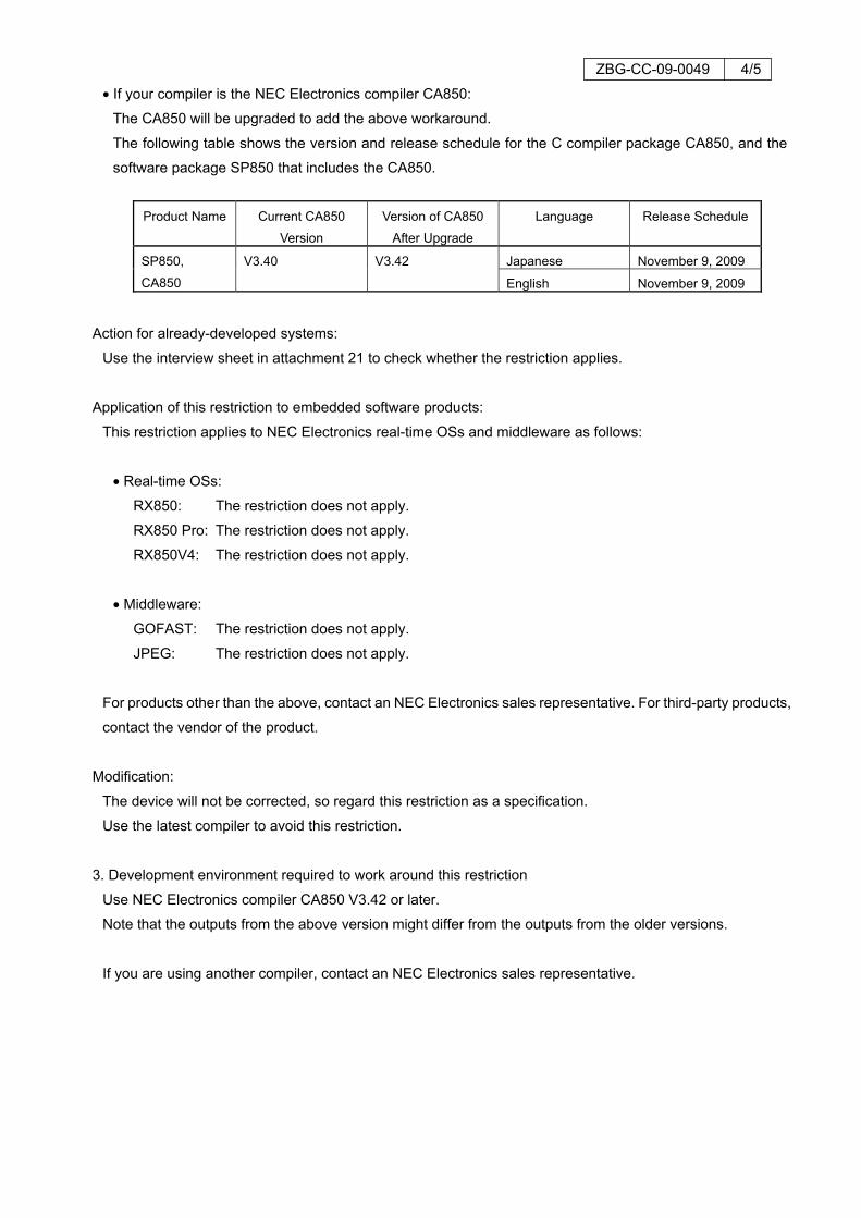
• If your compiler is the NEC Electronics compiler CA850:
The CA850 will be upgraded to add the above workaround.
The following table shows the version and release schedule for the C compiler package CA850, and the
software package SP850 that includes the CA850.
Product Name Current CA850
Version
Version of CA850
After Upgrade
Language Release Schedule
Japanese November 9, 2009 SP850,
CA850
V3.40 V3.42
English November 9, 2009
Action for already-developed systems:
Use the interview sheet in attachment 21 to check whether the restriction applies.
Application of this restriction to embedded software products:
This restriction applies to NEC Electronics real-time OSs and middleware as follows:
• Real-time OSs:
RX850: The restriction does not apply.
RX850 Pro: The restriction does not apply.
RX850V4: The restriction does not apply.
• Middleware:
GOFAST: The restriction does not apply.
JPEG: The restriction does not apply.
For products other than the above, contact an NEC Electronics sales representative. For third-party products,
contact the vendor of the product.
Modification:
The device will not be corrected, so regard this restriction as a specification.
Use the latest compiler to avoid this restriction.
3. Development environment required to work around this restriction
Use NEC Electronics compiler CA850 V3.42 or later.
Note that the outputs from the above version might differ from the outputs from the older versions.
If you are using another compiler, contact an NEC Electronics sales representative.
ZBG-CC-09-0049 5/5
4. Document revision history
Document Number Date Issued Description
SBG-DT-0091-E June 7, 2002 1st edition
SBG-DT-0096-E June 11, 2002 Correction of existing restrictions and errors in user’s manual
SBG-DT-0125-E August 31, 2002 Addition of restrictions
SBG-DT-0127-E September 25, 2002 Addition of restrictions
SBG-DT-03-0020-E December 3, 2002 Addition of restrictions
SBG-DT-03-0105-E March 18, 2003 Addition of restrictions
SBG-DT-03-0174-E June 13, 2003 Addition of restriction
SBG-DT-03-0278-E November 10, 2003 Correction of errors in user’s manual and addition of descriptions
SBG-DT-04-0052 February 9, 2004 Addition of restriction
ZBG-CC-09-0049 November 9, 2009 Addition of restriction (no. 3)
ZBG-CC-09-0049 Attachment 2-1
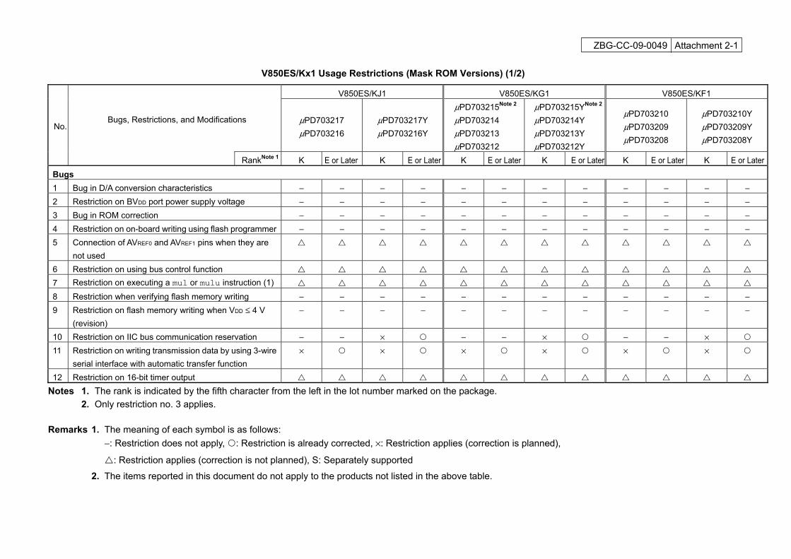
V850ES/Kx1 Usage Restrictions (Mask ROM Versions) (1/2)
V850ES/KJ1 V850ES/KG1 V850ES/KF1
Bugs, Restrictions, and Modifications μPD703217 μPD703216
μPD703217Y μPD703216Y
μPD703215Note 2 μPD703214 μPD703213 μPD703212
μPD703215YNote 2 μPD703214Y μPD703213Y μPD703212Y
μPD703210 μPD703209 μPD703208
μPD703210Y μPD703209Y μPD703208Y
No.
RankNote 1 K E or Later K E or Later K E or Later K E or Later K E or Later K E or Later
Bugs 1 Bug in D/A conversion characteristics − − − − − − − − − − − − 2 Restriction on BVDD port power supply voltage − − − − − − − − − − − − 3 Bug in ROM correction − − − − − − − − − − − − 4 Restriction on on-board writing using flash programmer − − − − − − − − − − − − 5 Connection of AVREF0 and AVREF1 pins when they are
not used
6 Restriction on using bus control function 7 Restriction on executing a mul or mulu instruction (1) 8 Restriction when verifying flash memory writing − − − − − − − − − − − − 9 Restriction on flash memory writing when VDD ≤ 4 V
(revision) − − − − − − − − − − − −
10 Restriction on IIC bus communication reservation − − × − − × − − × 11 Restriction on writing transmission data by using 3-wire
serial interface with automatic transfer function × × × × × ×
12 Restriction on 16-bit timer output Notes 1. The rank is indicated by the fifth character from the left in the lot number marked on the package. 2. Only restriction no. 3 applies. Remarks 1. The meaning of each symbol is as follows: −: Restriction does not apply, : Restriction is already corrected, ×: Restriction applies (correction is planned),
: Restriction applies (correction is not planned), S: Separately supported
2. The items reported in this document do not apply to the products not listed in the above table.
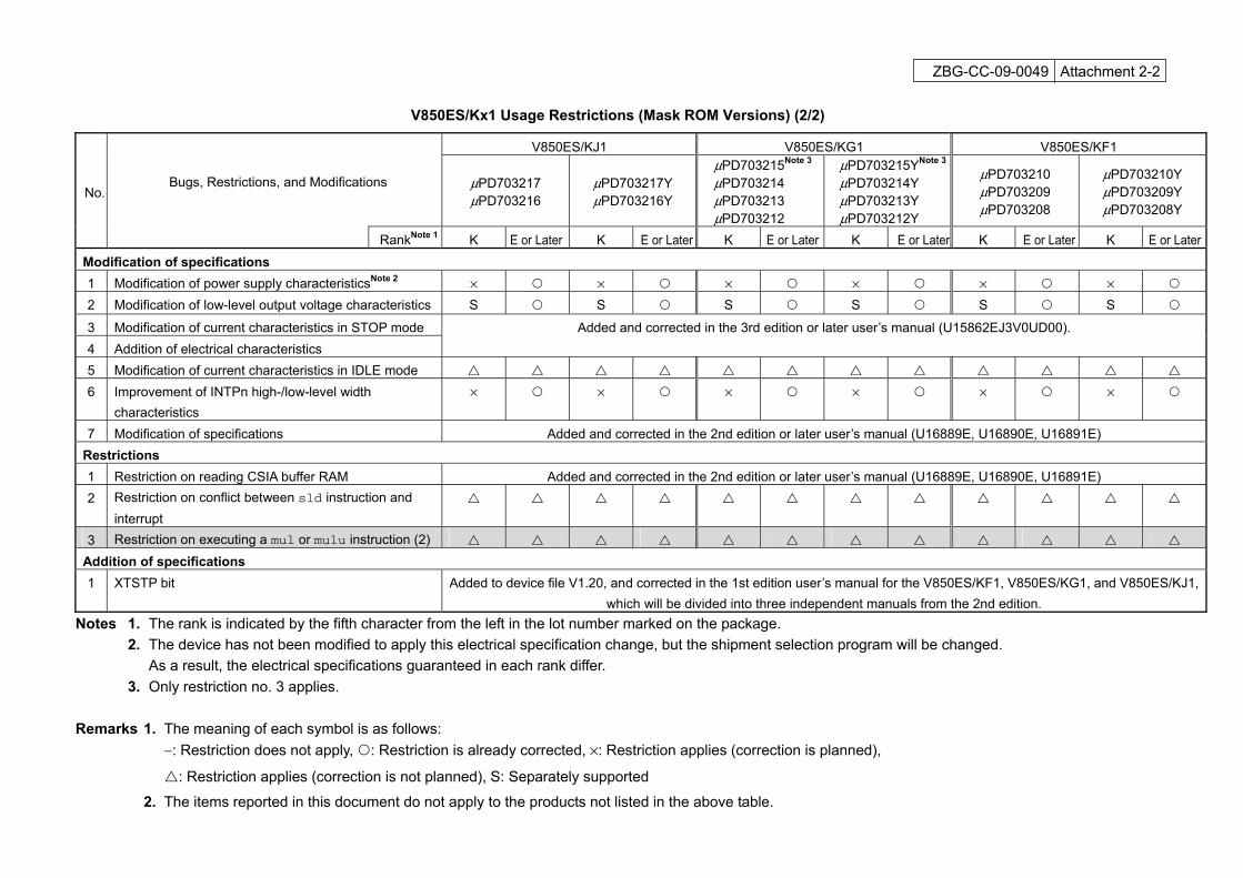
ZBG-CC-09-0049 Attachment 2-2
V850ES/Kx1 Usage Restrictions (Mask ROM Versions) (2/2)
V850ES/KJ1 V850ES/KG1 V850ES/KF1
Bugs, Restrictions, and Modifications μPD703217 μPD703216
μPD703217Y μPD703216Y
μPD703215Note 3 μPD703214 μPD703213 μPD703212
μPD703215YNote 3 μPD703214Y μPD703213Y μPD703212Y
μPD703210 μPD703209 μPD703208
μPD703210Y μPD703209Y μPD703208Y
No.
RankNote 1 K E or Later K E or Later K E or Later K E or Later K E or Later K E or Later Modification of specifications 1 Modification of power supply characteristicsNote 2 × × × × × × 2 Modification of low-level output voltage characteristics S S S S S S
3 Modification of current characteristics in STOP mode 4 Addition of electrical characteristics
Added and corrected in the 3rd edition or later user’s manual (U15862EJ3V0UD00).
5 Modification of current characteristics in IDLE mode 6 Improvement of INTPn high-/low-level width
characteristics × × × × × ×
7 Modification of specifications Added and corrected in the 2nd edition or later user’s manual (U16889E, U16890E, U16891E) Restrictions 1 Restriction on reading CSIA buffer RAM Added and corrected in the 2nd edition or later user’s manual (U16889E, U16890E, U16891E) 2 Restriction on conflict between sld instruction and
interrupt
3 Restriction on executing a mul or mulu instruction (2) Addition of specifications 1 XTSTP bit Added to device file V1.20, and corrected in the 1st edition user’s manual for the V850ES/KF1, V850ES/KG1, and V850ES/KJ1,
which will be divided into three independent manuals from the 2nd edition. Notes 1. The rank is indicated by the fifth character from the left in the lot number marked on the package. 2. The device has not been modified to apply this electrical specification change, but the shipment selection program will be changed. As a result, the electrical specifications guaranteed in each rank differ. 3. Only restriction no. 3 applies. Remarks 1. The meaning of each symbol is as follows: −: Restriction does not apply, : Restriction is already corrected, ×: Restriction applies (correction is planned),
: Restriction applies (correction is not planned), S: Separately supported
2. The items reported in this document do not apply to the products not listed in the above table.
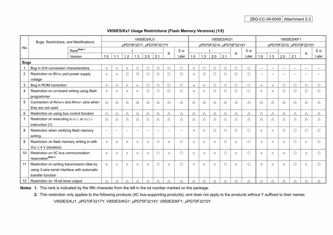
ZBG-CC-09-0049 Attachment 2-3
V850ES/Kx1 Usage Restrictions (Flash Memory Versions) (1/2)
V850ES/KJ1 V850ES/KG1 V850ES/KF1 Bugs, Restrictions, and Modifications
μPD70F3217, μPD70F3217Y μPD70F3214, μPD70F3214Y μPD70F3210, μPD70F3210Y RankNote 1 I I I
No.
Version 1.0 1.1 1.2 1.3 2.0 2.1 K
E or Later 1.0 1.3 2.0 2.1
K E or Later 1.0 1.3 2.0 2.1
K E or Later
Bugs 1 Bug in D/A conversion characteristics × × × × − − − − − − 2 Restriction on BVDD port power supply
voltage × × × − − − − − −
3 Bug in ROM correction × × × × × × × × 4 Restriction on on-board writing using flash
programmer × × × × × × × ×
5 Connection of AVREF0 and AVREF1 pins when they are not used
6 Restriction on using bus control function 7 Restriction on executing a mul or mulu
instruction (1)
8 Restriction when verifying flash memory writing
− − − − − − − − × × × ×
9 Restriction on flash memory writing in with VDD ≤ 4 V (revision)
× × × × × × × × × × × × × ×
10 Restriction on IIC bus communication reservationNote 2
× × × × × × × × × × × × × ×
11 Restriction on writing transmission data by using 3-wire serial interface with automatic transfer function
× × × × × × × × × × × × × ×
12 Restriction on 16-bit timer output
Notes 1. The rank is indicated by the fifth character from the left in the lot number marked on the package.
2. This restriction only applies to the following products (IIC bus-supporting products), and does not apply to the products without Y suffixed to their names.
V850ES/KJ1: μPD70F3217Y, V850ES/KG1: μPD70F3214Y, V850ES/KF1: μPD70F3210Y
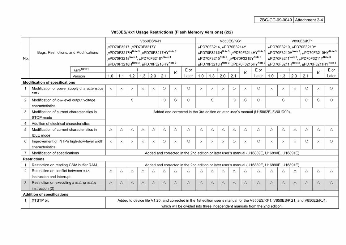
ZBG-CC-09-0049 Attachment 2-4
V850ES/Kx1 Usage Restrictions (Flash Memory Versions) (2/2)
V850ES/KJ1 V850ES/KG1 V850ES/KF1
Bugs, Restrictions, and Modifications μPD70F3217, μPD70F3217Y μPD70F3217HNote 3, μPD70F3217HYNote 3 μPD70F3218Note 3, μPD70F3218YNote 3 μPD70F3218HNote 3, μPD70F3218HYNote 3
μPD70F3214, μPD70F3214Y μPD70F3214HNote 3, μPD70F3214HYNote 3
μPD70F3215Note 3, μPD70F3215YNote 3 μPD70F3215HNote 3, μPD70F3215HYNote 3
μPD70F3210, μPD70F3210Y μPD70F3210HNote 3, μPD70F3210HYNote 3 μPD70F3211Note 3, μPD70F3211YNote 3 μPD70F3211HNote 3, μPD70F3211HYNote 3
RankNote 1 I I I
No.
Version 1.0 1.1 1.2 1.3 2.0 2.1
K E or Later 1.0 1.3 2.0 2.1
K E or Later 1.0 1.3 2.0 2.1
K E or Later
Modification of specifications 1 Modification of power supply characteristics
Note 2 × × × × × × × × × × × × × ×
2 Modification of low-level output voltage characteristics
S S S S S S
3 Modification of current characteristics in STOP mode
4 Addition of electrical characteristics
Added and corrected in the 3rd edition or later user’s manual (U15862EJ3V0UD00).
5 Modification of current characteristics in IDLE mode
6 Improvement of INTPn high-/low-level width characteristics
× × × × × × × × × × × × × ×
7 Modification of specifications Added and corrected in the 2nd edition or later user’s manual (U16889E, U16890E, U16891E) Restrictions 1 Restriction on reading CSIA buffer RAM Added and corrected in the 2nd edition or later user’s manual (U16889E, U16890E, U16891E) 2 Restriction on conflict between sld
instruction and interrupt
3 Restriction on executing a mul or mulu instruction (2)
Addition of specifications 1 XTSTP bit Added to device file V1.20, and corrected in the 1st edition user’s manual for the V850ES/KF1, V850ES/KG1, and V850ES/KJ1,
which will be divided into three independent manuals from the 2nd edition.
ZBG-CC-09-0049 Attachment 2-5
Notes 1. The rank is indicated by the fifth character from the left in the lot number marked on the package.
2. The device has not been modified to apply this electrical specification change, but the shipment selection program will be changed.
As a result, the electrical specifications guaranteed in each rank differ. 3. Only restriction no. 3 applies.
Remarks 1. The meaning of each symbol is as follows: −: Restriction does not apply, : Restriction is already corrected, ×: Restriction applies (correction is planned),
: Restriction applies (correction is not planned), S: Separately supported
2. The items reported in this document do not apply to the products not listed in the above table.
ZBG-CC-09-0049 Attachment 3
Bug Details
No. 1 Bug in D/A conversion characteristics Description:
If the D/A converter is running with AVREF1 (power supply for DAC) at 3.0 V or below, the conversion
accuracy does not satisfy the specifications.
Reference: Target specifications (as of May 28, 2002)
1.2 %FSR (load condition: 2 MΩ)
0.8 %FSR (load condition: 4 MΩ)
0.6 %FSR (load condition: 10 MΩ)
Workaround:
Use the D/A converter with AVREF1 higher than 3 V.
The circuit will be modified. The bug-corrected version will be shipped according to the following
schedule:
Modified sample for V850ES/KJ1: July 2002
Modified sample for V850ES/KG1: July 2002
For details about the schedule, contact an NEC Electronics sales representative or distributor.
No. 2 Restriction on BVDD port power supply voltage Description:
If the power supply voltage for the BVDD port is set to a voltage lower than that for other ports (VDD = EVDD
= AVREF0 ≥ BVDD) and BVDD = 3 V or lower, the I/O level of pins in the BVDD ports (see the list below)
becomes undefined.
However, if the power supply voltage for the BVDD port is the same as that of other ports (VDD = EVDD =
AVREF0 = BVDD) and BVDD = 2.7 V or higher, the operation is performed correctly because it is within the
guaranteed operation range.
BVDD ports:
• V850ES/KJ1: PCD0 to PCD3, PCM0 to PCM5, PCS0 to PCS7, PCT0 to PCT7,
PDH0 to PDH7, PDL0 to PDL15
• V850ES/KG1: PCM0 to PCM3, PCS0 to PCS1, PCT0 to PCT1/4/6, PDH0 to PDH5,
PDL0 to PDL15
• V850ES/KF1: PCM0 to PCM3, PCS0 to PCS1, PCT0 to PCT1/4/6, PDL0 to PDL15
Workaround:
Set the power supply voltage to VDD = EVDD = AVREF0 = BVDD ≥ 2.7 V. The circuit will be modified. The bug-corrected version will be shipped according to the following
schedule:
Modified sample for V850ES/KJ1: June 2002
Modified sample for V850ES/KG1: July 2002
For details about the schedule, contact an NEC Electronics sales representative or distributor.
ZBG-CC-09-0049 Attachment 4
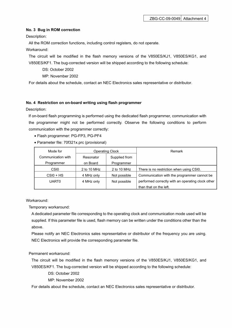
No. 3 Bug in ROM correction Description:
All the ROM correction functions, including control registers, do not operate.
Workaround:
The circuit will be modified in the flash memory versions of the V850ES/KJ1, V850ES/KG1, and
V850ES/KF1. The bug-corrected version will be shipped according to the following schedule:
DS: October 2002
MP: November 2002
For details about the schedule, contact an NEC Electronics sales representative or distributor.
No. 4 Restriction on on-board writing using flash programmer Description:
If on-board flash programming is performed using the dedicated flash programmer, communication with
the programmer might not be performed correctly. Observe the following conditions to perform
communication with the programmer correctly:
• Flash programmer: PG-FP3, PG-PF4
• Parameter file: 70f321x.prc (provisional)
Operating Clock Mode for
Communication with
Programmer Resonator
on Board
Supplied from
Programmer
Remark
CSI0 2 to 10 MHz 2 to 10 MHz There is no restriction when using CSI0.
CSI0 + HS 4 MHz only Not possible
UART0 4 MHz only Not possible
Communication with the programmer cannot be
performed correctly with an operating clock other
than that on the left.
Workaround:
Temporary workaround:
A dedicated parameter file corresponding to the operating clock and communication mode used will be
supplied. If this parameter file is used, flash memory can be written under the conditions other than the
above.
Please notify an NEC Electronics sales representative or distributor of the frequency you are using.
NEC Electronics will provide the corresponding parameter file.
Permanent workaround:
The circuit will be modified in the flash memory versions of the V850ES/KJ1, V850ES/KG1, and
V850ES/KF1. The bug-corrected version will be shipped according to the following schedule:
DS: October 2002
MP: November 2002
For details about the schedule, contact an NEC Electronics sales representative or distributor.
ZBG-CC-09-0049 Attachment 5
No. 5 Connection of AVREF0 and AVREF1 pins when they are not used Description:
In the V850ES/Kx1 Preliminary User’s Manual (U15862EJ1V0UM00), the recommended connection of
the unused AVREF0 and AVREF1 pins is incorrect.
Incorrect: Connect to VSS via a resistor.
Correct: Connect directly to VDD.
Workaround:
Permanent workaround:
This description will be corrected in future revisions of the user’s manual (U15862EJ2 or later).
For details about the schedule, contact an NEC Electronics sales representative or distributor.
ZBG-CC-09-0049 Attachment 6
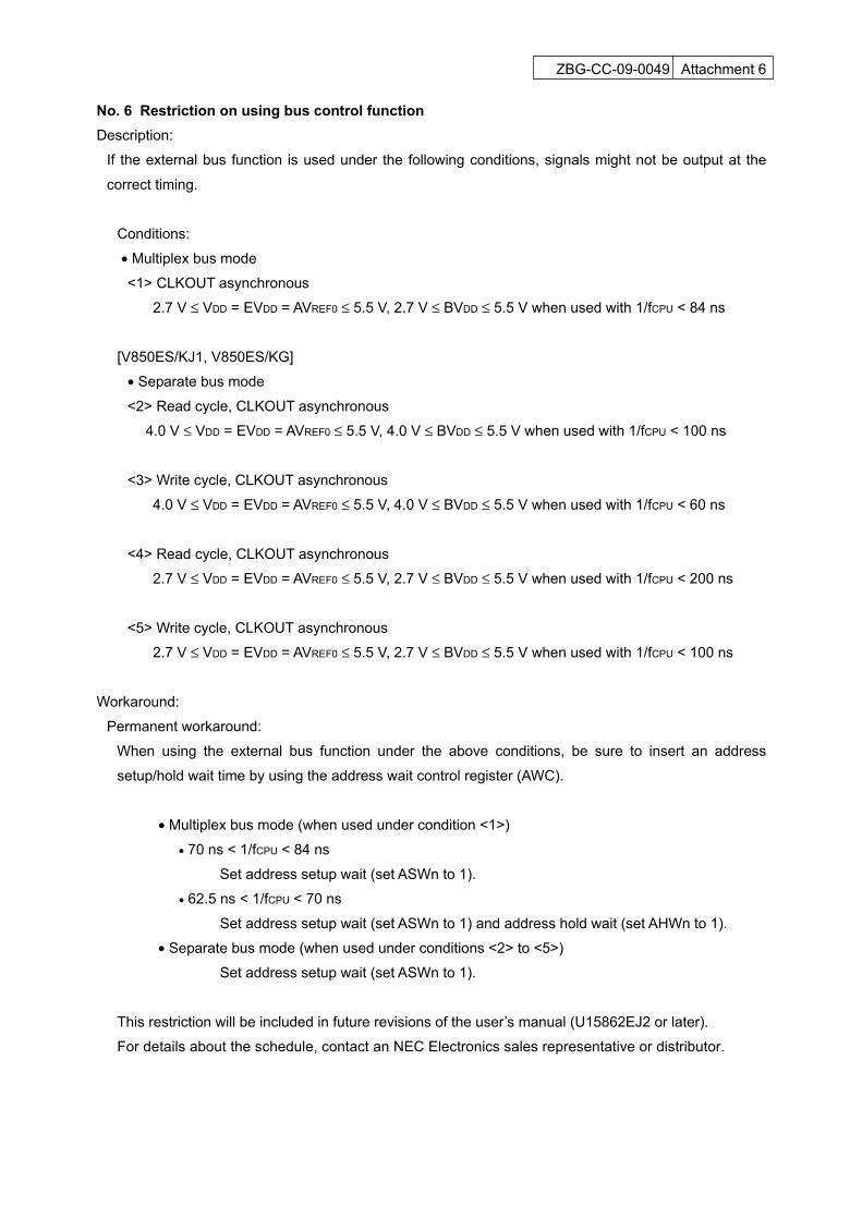
No. 6 Restriction on using bus control function Description:
If the external bus function is used under the following conditions, signals might not be output at the
correct timing.
Conditions:
• Multiplex bus mode
<1> CLKOUT asynchronous
2.7 V ≤ VDD = EVDD = AVREF0 ≤ 5.5 V, 2.7 V ≤ BVDD ≤ 5.5 V when used with 1/fCPU < 84 ns
[V850ES/KJ1, V850ES/KG]
• Separate bus mode
<2> Read cycle, CLKOUT asynchronous
4.0 V ≤ VDD = EVDD = AVREF0 ≤ 5.5 V, 4.0 V ≤ BVDD ≤ 5.5 V when used with 1/fCPU < 100 ns
<3> Write cycle, CLKOUT asynchronous
4.0 V ≤ VDD = EVDD = AVREF0 ≤ 5.5 V, 4.0 V ≤ BVDD ≤ 5.5 V when used with 1/fCPU < 60 ns
<4> Read cycle, CLKOUT asynchronous
2.7 V ≤ VDD = EVDD = AVREF0 ≤ 5.5 V, 2.7 V ≤ BVDD ≤ 5.5 V when used with 1/fCPU < 200 ns
<5> Write cycle, CLKOUT asynchronous
2.7 V ≤ VDD = EVDD = AVREF0 ≤ 5.5 V, 2.7 V ≤ BVDD ≤ 5.5 V when used with 1/fCPU < 100 ns
Workaround:
Permanent workaround:
When using the external bus function under the above conditions, be sure to insert an address
setup/hold wait time by using the address wait control register (AWC).
• Multiplex bus mode (when used under condition <1>)
• 70 ns < 1/fCPU < 84 ns
Set address setup wait (set ASWn to 1).
• 62.5 ns < 1/fCPU < 70 ns
Set address setup wait (set ASWn to 1) and address hold wait (set AHWn to 1).
• Separate bus mode (when used under conditions <2> to <5>)
Set address setup wait (set ASWn to 1).
This restriction will be included in future revisions of the user’s manual (U15862EJ2 or later).
For details about the schedule, contact an NEC Electronics sales representative or distributor.
ZBG-CC-09-0049 Attachment 7-1
No. 7 Restriction on executing a mul or mulu instruction (1)
Description: If an interrupt occurs during execution of a mul or mulu instruction that uses the same register for the first
and third operands, the operation result (register value of the third operand) might be invalid. The
execution of the instruction terminates and the subsequent instruction is executed.
The NEC Electronics C compiler CA850 does not generate instructions to which this restriction applies,
but this restriction applies if this kind of instruction is used in the assembler code. Use a function such as
global searching in your editor to check whether this kind of code exists.
See Related products below for information about GHS, Inc., Red Hat Inc. and Wind River Systems, Inc.
Example: mul reg1, reg2, reg1
mulu reg1, reg2, reg1
; Registers reg1 and reg2 are not the same. reg1 is not r0 (zero register).
This restriction does not apply if the register used for the first and third operands is not the same.
The CA850 does not generate the instruction format to which this restriction applies. In addition, the
real-time OSs RX850 and RX850 Pro and all middleware products do not use the instruction format to
which this restriction applies.
Workaround:
Specify the instruction code as shown below. mul reg1, reg2, reg3
And mulu reg1, reg2, reg3
; Registers reg1, reg2, and reg3 are not the same. reg3 is not r0.
Or mov reg1, rtmp
mul rtmp, reg2, reg1
And mov reg1, rtmp
mulu rtmp, reg2, reg1
; Registers reg1, reg2, and rtmp are not the same. reg1 and rtmp are not r0.
Related products:
• GHS compilers
For the C compiler up to Ver. 1.8.9, the instruction format to which this restriction applies might be selected and created if the embedded function __MULSH() or __MULUH() is used, depending on the
optimization mode setting.
ZBG-CC-09-0049 Attachment 7-2
Extract all the mul instructions by specifying % gdump a.out | grep mul for the gdump, a
disassembler included in the GHS compiler, to check whether the instruction to which this restriction
applies exists.
For MULTI 2000 Rel. 3.5 and later, this instruction format will not be created in both C source and
assembler source, and the instruction will be detected as an error when assembling the program.
MULTI 2000 Rel. 3.5 is scheduled for release in February 2002 in the US and March 2002 in Japan. For
the detailed schedule, contact an NEC Electronics sales representative. For the runtime library, the mul and mulu instructions are used but this instruction format is not.
• Products of Red Hat Inc. and Wind River Systems, Inc.
The GNU compiler from these companies does not create the instruction format to which this restriction
applies.
ZBG-CC-09-0049 Attachment 8
No. 8 Restriction when verifying flash memory writing Description:
An error might be output when writing to the flash memory is verified in the applicable product.
This bug occurs only for verification, and does not occur in a write or erase operation.
Workaround:
Temporary workaround:
Verify flash memory writing under any of the following conditions:
(1) VDD ≤ 4.0 V (The REGC pin is connected to VDD, and the regulator not running.)
(2) Connect the REGC pin to GND via a 10 μF resistor. (The regulator is running.)
(3) fx ≤ 4 MHz (under this condition, REGC pin connection and VDD voltage do not affect this bug.)
Permanent workaround:
This bug will be corrected in rank I V2.0 or later (or rank K or later).
For details about the schedule, contact an NEC Electronics sales representative or distributor.
Remark The rank is indicated by the fifth character from the left in the lot number marked on the
package.
ZBG-CC-09-0049 Attachment 9
No. 9 Restriction on flash memory writing when VDD ≤ 4 V (revised) Description:
Write, erase, and verify might not be performed correctly if the flash memory is written with VDD ≤ 4 V or
REGC = 10 μF (when the regulator is used).
(There is no problem in normal operation.)
Workaround:
Temporary workaround:
Perform write, erase, and verify on the flash memory with VDD > 4 V and REGC = VDD > 4 V.
Permanent workaround:
This bug will be corrected in rank I V2.1 or later (or rank E or later).
For details about the schedule, contact an NEC Electronics sales representative or distributor.
Remark The rank is indicated by the fifth character from the left in the lot number marked on the
package.
ZBG-CC-09-0049 Attachment 10
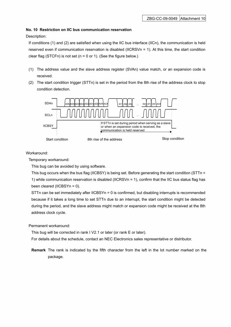
No. 10 Restriction on IIC bus communication reservation Description:
If conditions (1) and (2) are satisfied when using the IIC bus interface (IICn), the communication is held
reserved even if communication reservation is disabled (IICRSVn = 1). At this time, the start condition
clear flag (STCFn) is not set (n = 0 or 1). (See the figure below.)
(1) The address value and the slave address register (SVAn) value match, or an expansion code is
received.
(2) The start condition trigger (STTn) is set in the period from the 8th rise of the address clock to stop
condition detection.
Workaround:
Temporary workaround:
This bug can be avoided by using software.
This bug occurs when the bus flag (IICBSY) is being set. Before generating the start condition (STTn =
1) while communication reservation is disabled (IICRSVn = 1), confirm that the IIC bus status flag has
been cleared (IICBSYn = 0).
STTn can be set immediately after IICBSYn = 0 is confirmed, but disabling interrupts is recommended
because if it takes a long time to set STTn due to an interrupt, the start condition might be detected
during the period, and the slave address might match or expansion code might be received at the 8th
address clock cycle.
Permanent workaround:
This bug will be corrected in rank I V2.1 or later (or rank E or later).
For details about the schedule, contact an NEC Electronics sales representative or distributor.
Remark The rank is indicated by the fifth character from the left in the lot number marked on the
package.
AD6 AD5 AD4 AD3 AD2 AD1 AD0 R/W ACK …
…
D7 D6 D5 D2 D1 D0 ACK
Stop condition Start condition
IICBSY
SCLn
SDAn
8th rise of the address
If STTn is set during period when serving as a slave or when an expansion code is received, the communication is held reserved
ZBG-CC-09-0049 Attachment 11-1
No. 11 Restriction on writing transmission data by using 3-wire serial interface with automatic transfer function
Description:
If the 3-wire serial interface with automatic transfer function (CSIAn) is used to write data to be
transmitted to the buffer RAM (CSIAnBm), data might not be written correctly depending on the
instruction executed next to the write instruction (n = 0 or 1, m = 0 to F).
This restriction does not apply under the following condition:
Condition: CSIAn input clock (fSCKA) is faster than the CPU operating clock (fCPU) × 10
fCPU × 10 < fSCKA
fSCKA: CSIAn input clock selected by bits 6 and 7 (CKSAn0 and CKSAn1) of the CSIAn
status register (CSISn)
Workaround:
Temporary workarounds:
Do one of the workarounds below by using software. To avoid this restriction, it is required to use
instructions with the same access length until the write is complete.
Workaround 1: After data is written, read the data using a halfword access instruction (ST.H) and compare the values.
If the data do not match, write the data again. At this time, it is not necessary to disable interrupts.
When writing an odd number of bytes, write dummy data to the higher address of the buffer RAM
(CSIAnBmH). The halfword access instruction must be used to access registers until the comparison
result matches and written data is confirmed.
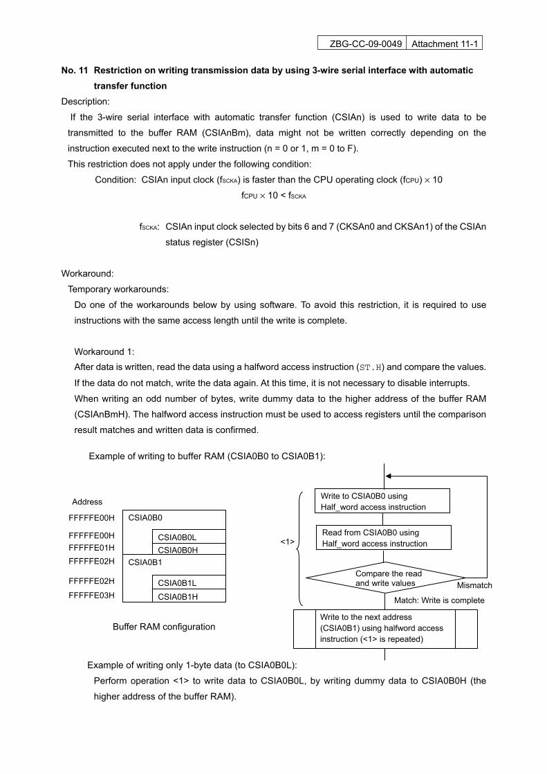
Example of writing to buffer RAM (CSIA0B0 to CSIA0B1):
Example of writing only 1-byte data (to CSIA0B0L):
Perform operation <1> to write data to CSIA0B0L, by writing dummy data to CSIA0B0H (the
higher address of the buffer RAM).
Write to the next address (CSIA0B1) using halfword access instruction (<1> is repeated)
Write to CSIA0B0 using Half_word access instruction
Read from CSIA0B0 using Half_word access instruction
Compare the read and write values
<1>
CSIA0B0
CSIA0B0H CSIA0B0L
CSIA0B1
CSIA0B1H CSIA0B1L
FFFFFE00H
FFFFFE00H FFFFFE01H FFFFFE02H
FFFFFE02H
FFFFFE03H
Address
Mismatch
Match: Write is complete
Buffer RAM configuration
ZBG-CC-09-0049 Attachment 11-2
Workaround 2: Execute the DI instruction to disable interrupts and execute only a halfword access instruction (ST.H)
to write data to the buffer RAM. In addition, write the last 2 bytes of the written data again. Do not
execute instructions other than NOP and arithmetic operation instructions between writing data to the
buffer RAM and writing the last 2 bytes.
When writing an odd number of bytes, write dummy data to the higher address of the buffer RAM
(CSIAnBmH).
Workaround 3: Execute the DI instruction to disable interrupts and execute only a byte access instruction (ST.B) to
write data to the buffer RAM. In addition, execute a NOP or arithmetic operation instruction for 5 or
more input clock cycles selected by bits 6 and 7 (CKSAn1 and CKSAn0) of the CSISn register after the
last data is written to the buffer RAM.
Permanent workaround:
This bug will be corrected in rank I V2.1 or later (or rank E or later).
For details about the schedule, contact an NEC Electronics sales representative or distributor.
Remark The rank is indicated by the fifth character from the left in the lot number marked on the
package.
ZBG-CC-09-0049 Attachment 12
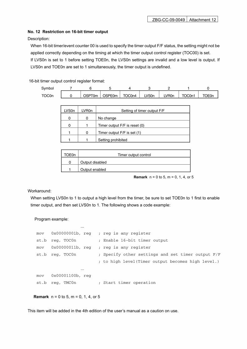
No. 12 Restriction on 16-bit timer output Description:
When 16-bit timer/event counter 00 is used to specify the timer output F/F status, the setting might not be
applied correctly depending on the timing at which the timer output control register (TOC00) is set.
If LVS0n is set to 1 before setting TOE0n, the LVS0n settings are invalid and a low level is output. If
LVS0n and TOE0n are set to 1 simultaneously, the timer output is undefined.
16-bit timer output control register format:
Symbol 7 6 5 4 3 2 1 0
TOC0n 0 OSPT0m OSPE0m TOC0n4 LVS0n LVR0n TOC0n1 TOE0n
LVS0n LVR0n Setting of timer output F/F
0 0 No change
0 1 Timer output F/F is reset (0)
1 0 Timer output F/F is set (1)
1 1 Setting prohibited
TOE0n Timer output control
0 Output disabled
1 Output enabled
Remark n = 0 to 5, m = 0, 1, 4, or 5
Workaround:
When setting LVS0n to 1 to output a high level from the timer, be sure to set TOE0n to 1 first to enable
timer output, and then set LVS0n to 1. The following shows a code example:
Program example:
... mov 0x00000001b, reg ; reg is any register
st.b reg, TOC0n ; Enable 16-bit timer output
mov 0x00000011b, reg ; reg is any register
st.b reg, TOC0n ; Specify other settings and set timer output F/F
; to high level(Timer output becomes high level.)
... mov 0x00001100b, reg
st.b reg, TMC0n ; Start timer operation
Remark n = 0 to 5, m = 0, 1, 4, or 5
This item will be added in the 4th edition of the user’s manual as a caution on use.
ZBG-CC-09-0049 Attachment 13-1
Specification Change Details No. 1 Modification of power supply characteristics Description:
As a result of evaluation, the TYP and MAX values of the power supply characteristics have been
improved (reduced).
This is just an improvement according to evaluation. The device has not been modified to include this
improvement.
The power supply characteristics before and after modification are attachment 13-2 (flash memory
versions) and 13-3 (mask ROM versions).
Application to products:
This modification will be applied to the following products:
Mask ROM versions: Rank E or later
Flash memory versions: Rank I V2.1 or later and rank E or later
The performance of the power supply characteristics in versions and ranks other than above does not
differ (excluding device-unique performance).
The device has not been modified to apply this electrical specification change, but the shipment selection
program will be changed. As a result, the electrical specifications guaranteed in each rank differ.
ZBG-CC-09-0049 Attachment 13-2
DC Characteristics (TA = −40 to +85°C, VDD = EVDD = AVREF0 = 2.7 to 5.5 V, 2.7 V ≤ BVDD ≤ VDD, 2.7 V ≤ AVREF1 ≤ VDD, VSS =
EVSS = BVSS = AVSS = 0 V) Before Change After Change Parameter Symbol Conditions
MIN. TYP. MAX. MIN. TYP. MAX.
Unit
fXX = 20 MHz (OSC = 5 MHz)
(in PLL mode)
REGC = VDD = 5 V ±10%
58 80 43 60 mA
fXX = 16 MHz (OSC = 4 MHz)
(in PLL mode)
REGC = Capacitor
VDD = 5 V ±10%
37 52 27 40 mA
IDD1 Normal
operation
fXX = 10 MHz (OSC = 10 MHz)
REGC = VDD = 3 V ±10%
25 35 14 29 mA
fXX = 20 MHz (OSC = 5 MHz)
(in PLL mode)
REGC = VDD = 5 V ±10%
25 35 18 28 mA
fXX = 16 MHz (OSC = 4 MHz)
(in PLL mode)
REGC = Capacitor
VDD = 5 V ±10%
14 25 11 20 mA
IDD2 HALT mode
fXX = 10 MHz (OSC = 10 MHz)
REGC = VDD = 3 V ±10%
9 14 6 11 mA
OSC = 5 MHz
(when PLL mode is off)
REGC = VDD = 5 V ±10%
1200 2000 1200 2000 μA
OSC = 4 MHz
(when PLL mode is off)
REGC = Capacitor
VDD = 5 V ±10%
900 1600 900 1600 μA
IDD3 IDLE mode
OSC = 10 MHz
(when PLL mode is off)
REGC = VDD = 3 V ±10%
900 1600 900 1600 μA
IDD4 Subclock
operating
mode
fXT = 32.768 kHz 260 370 190 320 μA
IDD5 Subclock
IDLE mode
fXT = 32.768 kHz 15 60 15 60 μA
Supply
currentNote 1
(flash memory
version)
IDD6 STOP mode 0.8 30 0.1
Note 2
30 μA
Notes 1. This is the total current for VDD, EVDD, and BVDD (when all ports are stopped), and does not
include AVREF0.
2. Point revised in this edition (previous edition: SBG-DT-0127-E). See attachment 15 for details.
ZBG-CC-09-0049 Attachment 13-3
DC Characteristics (TA = −40 to +85°C, VDD = EVDD = AVREF0 = 2.7 to 5.5 V, 2.7 V ≤ BVDD ≤ VDD, 2.7 V ≤ AVREF1 ≤ VDD, VSS =
EVSS = BVSS = AVSS = 0 V) Before Change After Change Parameter Symbol Conditions
MIN TYP MAX MIN TYP MAX
Unit
fXX = 20 MHz (OSC = 5 MHz)
(in PLL mode)
REGC = VDD = 5 V ±10%
43 65 30 45 mA
fXX = 16 MHz (OSC = 4 MHz)
(in PLL mode)
REGC = Capacitor
VDD = 5 V ±10%
25 38 18 30 mA
IDD1 Normal
operation
fXX = 10 MHz (OSC = 10 MHz)
REGC = VDD = 3 V ±10%
15 22 9 18 mA
fXX = 20 MHz (OSC = 5 MHz)
(in PLL mode)
REGC = VDD = 5 V ±10%
24 30 17 25 mA
fXX = 16 MHz (OSC = 4 MHz)
(in PLL mode)
REGC = Capacitor
VDD = 5 V ±10%
13 22 10 18 mA
IDD2 HALT mode
fXX = 10 MHz (OSC = 10 MHz)
REGC = VDD = 3 V ±10%
8 13 5 10 mA
OSC = 5 MHz
(when PLL mode is off)
REGC = VDD = 5 V ±10%
900 1400 900 1400 μA
OSC = 4 MHz
(when PLL mode is off)
REGC = Capacitor
VDD = 5 V ±10%
600 1000 600 1000 μA
IDD3 IDLE mode
OSC = 10 MHz
(when PLL mode is off)
REGC = VDD = 3 V ±10%
600 1000 600 1000 μA
IDD4 Subclock
operating
mode
fXT = 32.768 kHz 110 160 70 160 μA
IDD5 Subclock
IDLE mode
fXT = 32.768 kHz 15 60 15 60 μA
Supply
currentNote 1
(mask ROM
version)
IDD6 STOP mode 0.8 30 0.1
Note 2
30 μA
Notes 1. This is the total current for VDD, EVDD, and BVDD (when all ports are stopped), and does not
include AVREF0.
2. Point revised in this edition (previous edition: SBG-DT-0127-E). See attachment 15 for details.
ZBG-CC-09-0049 Attachment 14
No. 2 Modification of low-level output voltage characteristics Description:
The specifications of the low-level output voltage characteristics (VOL4) have been changed as follows:
Low-level output voltage characteristics (VOL4: P36 to P39)
Target devices: All flash memory and mask ROM versions Item Before Change After Change
Conditions Max. Conditions Max.
IOL = 8 mA EVDD = 3.0 to 5.5 V
1.0 V
VOL4
P32 to P39 IOL = 8 mA
EVDD = 2.7 to 5.5 V
1.0 V
IOL = 5 mA
EVDD = 2.7 to 5.5 V
1.0 V
Action:
This change will be applied to future revisions of the user’s manual (U15862EJ3 or later).
NEC Electronics will provide support for customers using products with the specification before change.
This change will be applied to the mask ROM and flash memory versions with rank E.
ZBG-CC-09-0049 Attachment 15
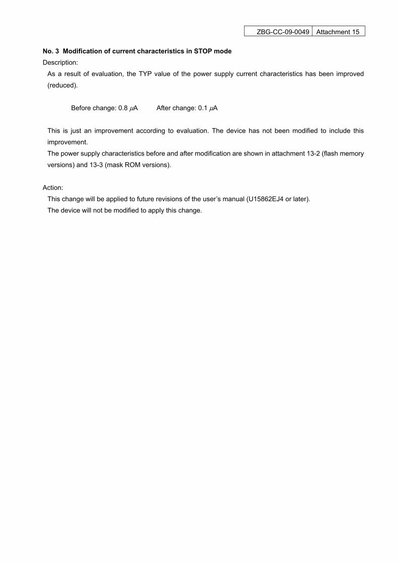
No. 3 Modification of current characteristics in STOP mode Description:
As a result of evaluation, the TYP value of the power supply current characteristics has been improved
(reduced).
Before change: 0.8 μA After change: 0.1 μA
This is just an improvement according to evaluation. The device has not been modified to include this
improvement.
The power supply characteristics before and after modification are shown in attachment 13-2 (flash memory
versions) and 13-3 (mask ROM versions).
Action:
This change will be applied to future revisions of the user’s manual (U15862EJ4 or later).
The device will not be modified to apply this change.
ZBG-CC-09-0049 Attachment 16
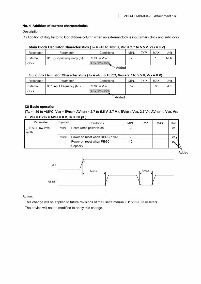
No. 4 Addition of current characteristics Description:
(1) Addition of duty factor to Conditions column when an external clock is input (main clock and subclock)
Main Clock Oscillator Characteristics (TA = −40 to +85°C, VDD = 2.7 to 5.5 V, VSS = 0 V) Resonator Parameter Conditions MIN. TYP. MAX. Unit
External
clock
X1, X2 input frequency (fX) REGC = VDD
Duty 50% ±5%
2 10 MHz
Subclock Oscillator Characteristics (TA = −40 to +85°C, VDD = 2.7 to 5.5 V, VSS = 0 V) Resonator Parameter Conditions MIN. TYP. MAX. Unit
External
clock
XT1 input frequency (fXT) REGC = VDD
Duty 50% ±5%
32 35 kHz
(2) Basic operation (TA = −40 to +85°C, VDD = EVDD = AVREF0 = 2.7 to 5.5 V, 2.7 V ≤ BVDD ≤ VDD, 2.7 V ≤ AVREF1 ≤ VDD, VSS = EVSS = BVSS = AVSS = 0 V, CL = 50 pF)
Parameter Symbol Conditions MIN. TYP. MAX. Unit _RESET low-level width
tWRSL1 Reset when power is on 2 μs
tWRSL2 Power-on reset when REGC = VDD 2 μs Power-on reset when REGC =
Capacity 10 μs
_RESET
VDD
tWRSL1tWRSL2
Action:
This change will be applied to future revisions of the user’s manual (U15862EJ3 or later).
The device will not be modified to apply this change.
Added
Added
Added
ZBG-CC-09-0049 Attachment 17
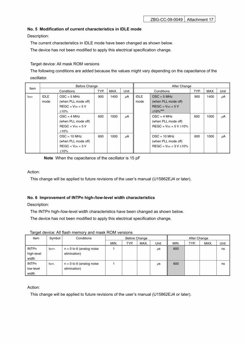
No. 5 Modification of current characteristics in IDLE mode Description:
The current characteristics in IDLE mode have been changed as shown below.
The device has not been modified to apply this electrical specification change.
Target device: All mask ROM versions
The following conditions are added because the values might vary depending on the capacitance of the
oscillator.
Before Change After Change Item
Conditions TYP. MAX. Unit Conditions TYP. MAX. Unit
OSC = 5 MHz
(when PLL mode off)
REGC = VDD = 5 V
±10%
900 1400 μA OSC = 5 MHz
(when PLL mode off)
REGC = VDD = 5 V
±10%Note
900 1400 μA
OSC = 4 MHz
(when PLL mode off)
REGC = VDD = 5 V
±10%
600 1000 μA OSC = 4 MHz
(when PLL mode off)
REGC = VDD = 5 V ±10%
600
1000
μA
IDD3 IDLE
mode
OSC = 10 MHz
(when PLL mode off)
REGC = VDD = 3 V
±10%
600 1000 μA
IDLE
mode
OSC = 10 MHz
(when PLL mode off)
REGC = VDD = 3 V ±10%
600 1000 μA
Note When the capacitance of the oscillator is 15 pF
Action:
This change will be applied to future revisions of the user’s manual (U15862EJ4 or later).
No. 6 Improvement of INTPn high-/low-level width characteristics Description:
The INTPn high-/low-level width characteristics have been changed as shown below.
The device has not been modified to apply this electrical specification change.
Target device: All flash memory and mask ROM versions Before Change After Change Item Symbol Conditions
MIN. TYP. MAX. Unit MIN. TYP. MAX. Unit
INTPn
high-level
width
tWITH n = 0 to 6 (analog noise
elimination)
1 μs 600 ns
INTPn
low-level
width
tWITL n = 0 to 6 (analog noise
elimination)
1 μs 600 ns
Action:
This change will be applied to future revisions of the user’s manual (U15862EJ4 or later).
ZBG-CC-09-0049 Attachment 18-1
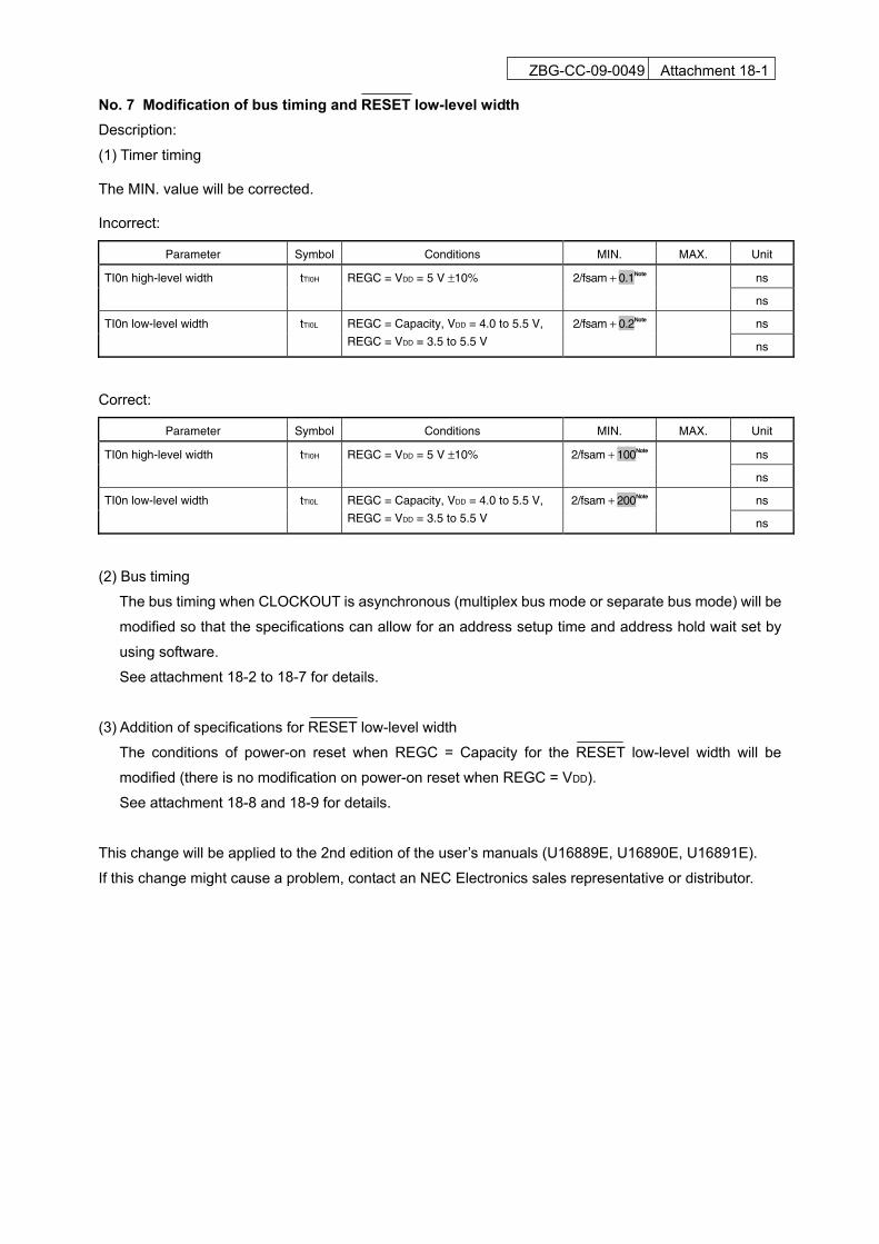
No. 7 Modification of bus timing and RESET low-level width Description:
(1) Timer timing
The MIN. value will be corrected.
Incorrect:
Parameter Symbol Conditions MIN. MAX. Unit
ns TI0n high-level width tTI0H REGC = VDD = 5 V ±10% 2/fsam + 0.1Note
ns
ns TI0n low-level width tTI0L REGC = Capacity, VDD = 4.0 to 5.5 V,
REGC = VDD = 3.5 to 5.5 V
2/fsam + 0.2Note
ns
Correct:
Parameter Symbol Conditions MIN. MAX. Unit
ns TI0n high-level width tTI0H REGC = VDD = 5 V ±10% 2/fsam + 100Note
ns
ns TI0n low-level width tTI0L REGC = Capacity, VDD = 4.0 to 5.5 V,
REGC = VDD = 3.5 to 5.5 V
2/fsam + 200Note
ns
(2) Bus timing
The bus timing when CLOCKOUT is asynchronous (multiplex bus mode or separate bus mode) will be
modified so that the specifications can allow for an address setup time and address hold wait set by
using software.
See attachment 18-2 to 18-7 for details.
(3) Addition of specifications for RESET low-level width
The conditions of power-on reset when REGC = Capacity for the RESET low-level width will be
modified (there is no modification on power-on reset when REGC = VDD).
See attachment 18-8 and 18-9 for details.
This change will be applied to the 2nd edition of the user’s manuals (U16889E, U16890E, U16891E).
If this change might cause a problem, contact an NEC Electronics sales representative or distributor.
ZBG-CC-09-0049 Attachment 18-2
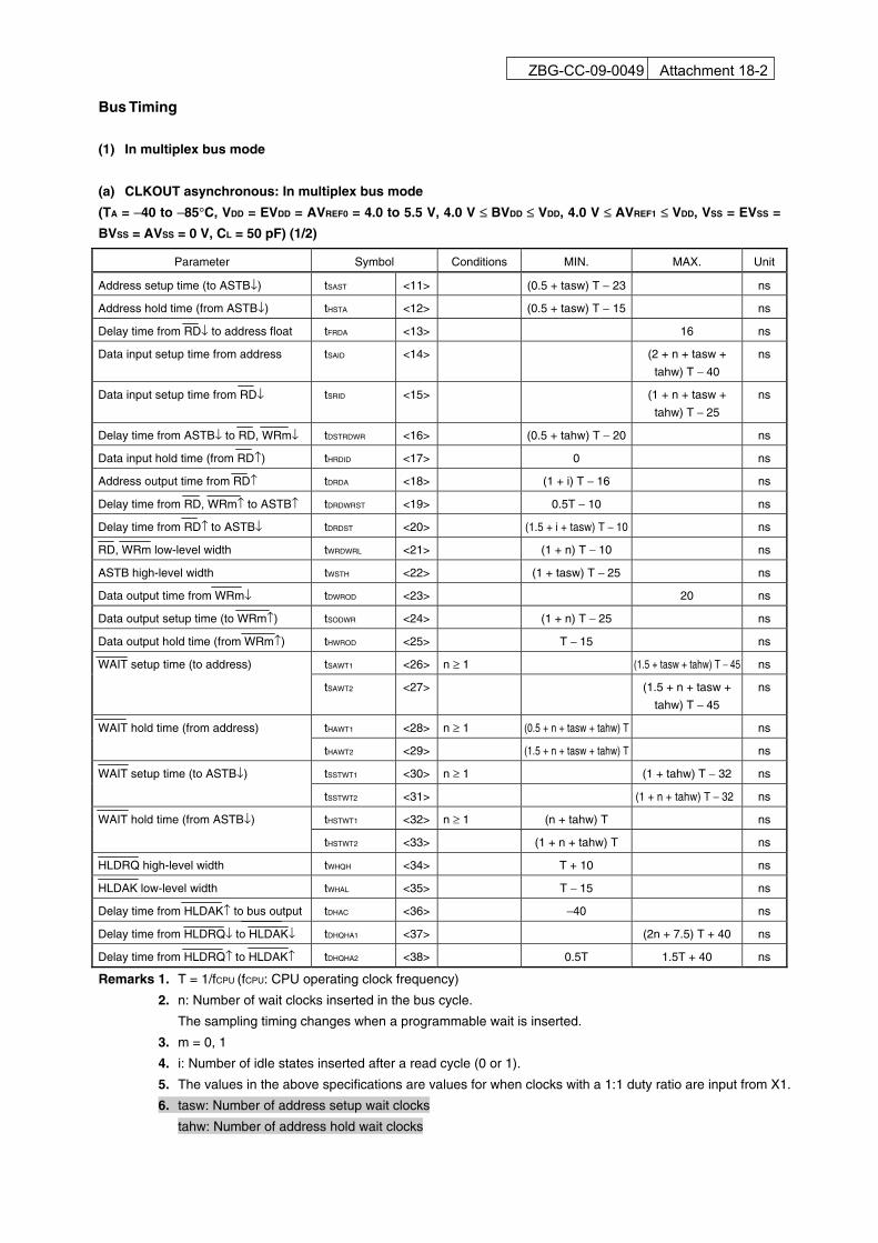
Bus Timing (1) In multiplex bus mode
(a) CLKOUT asynchronous: In multiplex bus mode
(TA = −40 to −85°C, VDD = EVDD = AVREF0 = 4.0 to 5.5 V, 4.0 V ≤ BVDD ≤ VDD, 4.0 V ≤ AVREF1 ≤ VDD, VSS = EVSS =
BVSS = AVSS = 0 V, CL = 50 pF) (1/2)
Parameter Symbol Conditions MIN. MAX. Unit
Address setup time (to ASTB↓) tSAST <11> (0.5 + tasw) T − 23 ns
Address hold time (from ASTB↓) tHSTA <12> (0.5 + tasw) T − 15 ns
Delay time from RD↓ to address float tFRDA <13> 16 ns
Data input setup time from address tSAID <14> (2 + n + tasw +
tahw) T − 40
ns
Data input setup time from RD↓ tSRID <15> (1 + n + tasw +
tahw) T − 25
ns
Delay time from ASTB↓ to RD, WRm↓ tDSTRDWR <16> (0.5 + tahw) T − 20 ns
Data input hold time (from RD↑) tHRDID <17> 0 ns
Address output time from RD↑ tDRDA <18> (1 + i) T − 16 ns
Delay time from RD, WRm↑ to ASTB↑ tDRDWRST <19> 0.5T − 10 ns
Delay time from RD↑ to ASTB↓ tDRDST <20> (1.5 + i + tasw) T − 10 ns
RD, WRm low-level width tWRDWRL <21> (1 + n) T − 10 ns
ASTB high-level width tWSTH <22> (1 + tasw) T − 25 ns
Data output time from WRm↓ tDWROD <23> 20 ns
Data output setup time (to WRm↑) tSODWR <24> (1 + n) T − 25 ns
Data output hold time (from WRm↑) tHWROD <25> T − 15 ns
tSAWT1 <26> n ≥ 1 (1.5 + tasw + tahw) T − 45 ns WAIT setup time (to address)
tSAWT2 <27> (1.5 + n + tasw +
tahw) T − 45
ns
tHAWT1 <28> n ≥ 1 (0.5 + n + tasw + tahw) T ns WAIT hold time (from address)
tHAWT2 <29> (1.5 + n + tasw + tahw) T ns
tSSTWT1 <30> n ≥ 1 (1 + tahw) T − 32 ns WAIT setup time (to ASTB↓)
tSSTWT2 <31> (1 + n + tahw) T − 32 ns
tHSTWT1 <32> n ≥ 1 (n + tahw) T ns WAIT hold time (from ASTB↓)
tHSTWT2 <33> (1 + n + tahw) T ns
HLDRQ high-level width tWHQH <34> T + 10 ns
HLDAK low-level width tWHAL <35> T − 15 ns
Delay time from HLDAK↑ to bus output tDHAC <36> −40 ns
Delay time from HLDRQ↓ to HLDAK↓ tDHQHA1 <37> (2n + 7.5) T + 40 ns
Delay time from HLDRQ↑ to HLDAK↑ tDHQHA2 <38> 0.5T 1.5T + 40 ns
Remarks 1. T = 1/fCPU (fCPU: CPU operating clock frequency)
2. n: Number of wait clocks inserted in the bus cycle.
The sampling timing changes when a programmable wait is inserted.
3. m = 0, 1
4. i: Number of idle states inserted after a read cycle (0 or 1).
5. The values in the above specifications are values for when clocks with a 1:1 duty ratio are input from X1.
6. tasw: Number of address setup wait clocks
tahw: Number of address hold wait clocks
ZBG-CC-09-0049 Attachment 18-3
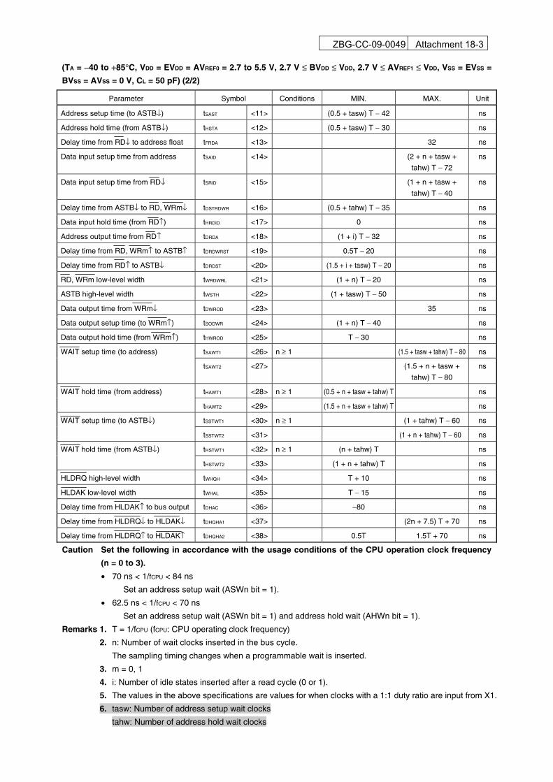
(TA = −40 to +85°C, VDD = EVDD = AVREF0 = 2.7 to 5.5 V, 2.7 V ≤ BVDD ≤ VDD, 2.7 V ≤ AVREF1 ≤ VDD, VSS = EVSS =
BVSS = AVSS = 0 V, CL = 50 pF) (2/2)
Parameter Symbol Conditions MIN. MAX. Unit
Address setup time (to ASTB↓) tSAST <11> (0.5 + tasw) T − 42 ns
Address hold time (from ASTB↓) tHSTA <12> (0.5 + tasw) T − 30 ns
Delay time from RD↓ to address float tFRDA <13> 32 ns
Data input setup time from address tSAID <14> (2 + n + tasw +
tahw) T − 72
ns
Data input setup time from RD↓ tSRID <15> (1 + n + tasw +
tahw) T − 40
ns
Delay time from ASTB↓ to RD, WRm↓ tDSTRDWR <16> (0.5 + tahw) T − 35 ns
Data input hold time (from RD↑) tHRDID <17> 0 ns
Address output time from RD↑ tDRDA <18> (1 + i) T − 32 ns
Delay time from RD, WRm↑ to ASTB↑ tDRDWRST <19> 0.5T − 20 ns
Delay time from RD↑ to ASTB↓ tDRDST <20> (1.5 + i + tasw) T − 20 ns
RD, WRm low-level width tWRDWRL <21> (1 + n) T − 20 ns
ASTB high-level width tWSTH <22> (1 + tasw) T − 50 ns
Data output time from WRm↓ tDWROD <23> 35 ns
Data output setup time (to WRm↑) tSODWR <24> (1 + n) T − 40 ns
Data output hold time (from WRm↑) tHWROD <25> T − 30 ns
tSAWT1 <26> n ≥ 1 (1.5 + tasw + tahw) T − 80 ns WAIT setup time (to address)
tSAWT2 <27> (1.5 + n + tasw +
tahw) T − 80
ns
tHAWT1 <28> n ≥ 1 (0.5 + n + tasw + tahw) T ns WAIT hold time (from address)
tHAWT2 <29> (1.5 + n + tasw + tahw) T ns
tSSTWT1 <30> n ≥ 1 (1 + tahw) T − 60 ns WAIT setup time (to ASTB↓)
tSSTWT2 <31> (1 + n + tahw) T − 60 ns
tHSTWT1 <32> n ≥ 1 (n + tahw) T ns WAIT hold time (from ASTB↓)
tHSTWT2 <33> (1 + n + tahw) T ns
HLDRQ high-level width tWHQH <34> T + 10 ns
HLDAK low-level width tWHAL <35> T − 15 ns
Delay time from HLDAK↑ to bus output tDHAC <36> −80 ns
Delay time from HLDRQ↓ to HLDAK↓ tDHQHA1 <37> (2n + 7.5) T + 70 ns
Delay time from HLDRQ↑ to HLDAK↑ tDHQHA2 <38> 0.5T 1.5T + 70 ns
Caution Set the following in accordance with the usage conditions of the CPU operation clock frequency
(n = 0 to 3).
• 70 ns < 1/fCPU < 84 ns
Set an address setup wait (ASWn bit = 1).
• 62.5 ns < 1/fCPU < 70 ns
Set an address setup wait (ASWn bit = 1) and address hold wait (AHWn bit = 1).
Remarks 1. T = 1/fCPU (fCPU: CPU operating clock frequency)
2. n: Number of wait clocks inserted in the bus cycle.
The sampling timing changes when a programmable wait is inserted.
3. m = 0, 1
4. i: Number of idle states inserted after a read cycle (0 or 1).
5. The values in the above specifications are values for when clocks with a 1:1 duty ratio are input from X1.
6. tasw: Number of address setup wait clocks
tahw: Number of address hold wait clocks
ZBG-CC-09-0049 Attachment 18-4
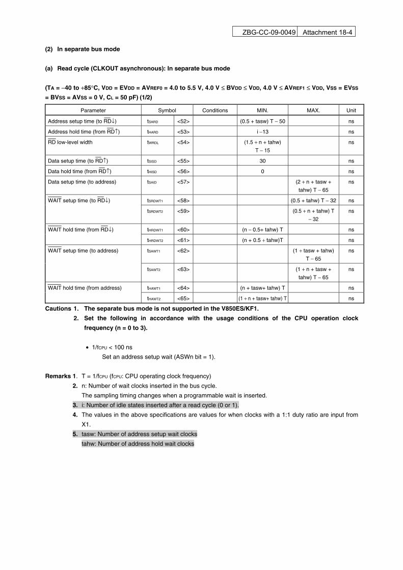
(2) In separate bus mode
(a) Read cycle (CLKOUT asynchronous): In separate bus mode
(TA = −40 to +85°C, VDD = EVDD = AVREF0 = 4.0 to 5.5 V, 4.0 V ≤ BVDD ≤ VDD, 4.0 V ≤ AVREF1 ≤ VDD, VSS = EVSS
= BVSS = AVSS = 0 V, CL = 50 pF) (1/2)
Parameter Symbol Conditions MIN. MAX. Unit
Address setup time (to RD↓) tSARD <52> (0.5 + tasw) T − 50 ns
Address hold time (from RD↑) tHARD <53> i −13 ns
RD low-level width tWRDL <54> (1.5 + n + tahw)
T − 15
ns
Data setup time (to RD↑) tSISD <55> 30 ns
Data hold time (from RD↑) tHISD <56> 0 ns
Data setup time (to address) tSAID <57> (2 + n + tasw +
tahw) T − 65
ns
tSRDWT1 <58> (0.5 + tahw) T − 32 ns WAIT setup time (to RD↓)
tSRDWT2 <59> (0.5 + n + tahw) T
− 32
ns
tHRDWT1 <60> (n − 0.5+ tahw) T ns WAIT hold time (from RD↓)
tHRDWT2 <61> (n + 0.5 + tahw)T ns
tSAWT1 <62> (1 + tasw + tahw)
T − 65
ns WAIT setup time (to address)
tSAWT2 <63> (1 + n + tasw +
tahw) T − 65
ns
tHAWT1 <64> (n + tasw+ tahw) T ns WAIT hold time (from address)
tHAWT2 <65> (1 + n + tasw+ tahw) T ns
Cautions 1. The separate bus mode is not supported in the V850ES/KF1.
2. Set the following in accordance with the usage conditions of the CPU operation clock
frequency (n = 0 to 3).
• 1/fCPU < 100 ns
Set an address setup wait (ASWn bit = 1).
Remarks 1. T = 1/fCPU (fCPU: CPU operating clock frequency)
2. n: Number of wait clocks inserted in the bus cycle.
The sampling timing changes when a programmable wait is inserted.
3. i: Number of idle states inserted after a read cycle (0 or 1).
4. The values in the above specifications are values for when clocks with a 1:1 duty ratio are input from
X1.
5. tasw: Number of address setup wait clocks
tahw: Number of address hold wait clocks
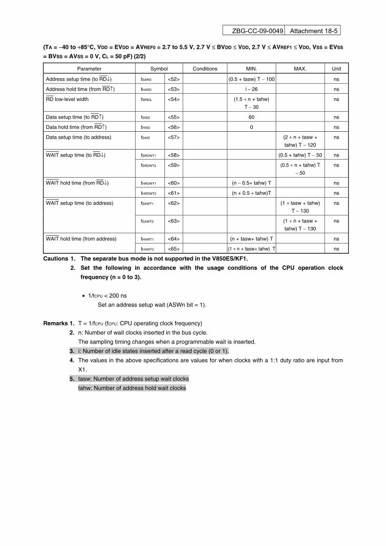
ZBG-CC-09-0049 Attachment 18-5
(TA = −40 to +85°C, VDD = EVDD = AVREF0 = 2.7 to 5.5 V, 2.7 V ≤ BVDD ≤ VDD, 2.7 V ≤ AVREF1 ≤ VDD, VSS = EVSS
= BVSS = AVSS = 0 V, CL = 50 pF) (2/2)
Parameter Symbol Conditions MIN. MAX. Unit
Address setup time (to RD↓) tSARD <52> (0.5 + tasw) T − 100 ns
Address hold time (from RD↑) tHARD <53> i − 26 ns
RD low-level width tWRDL <54> (1.5 + n + tahw)
T − 30
ns
Data setup time (to RD↑) tSISD <55> 60 ns
Data hold time (from RD↑) tHISD <56> 0 ns
Data setup time (to address) tSAID <57> (2 + n + tasw +
tahw) T − 120
ns
tSRDWT1 <58> (0.5 + tahw) T − 50 ns WAIT setup time (to RD↓)
tSRDWT2 <59> (0.5 + n + tahw) T
− 50
ns
tHRDWT1 <60> (n − 0.5+ tahw) T ns WAIT hold time (from RD↓)
tHRDWT2 <61> (n + 0.5 + tahw)T ns
tSAWT1 <62> (1 + tasw + tahw)
T − 130
ns WAIT setup time (to address)
tSAWT2 <63> (1 + n + tasw +
tahw) T − 130
ns
tHAWT1 <64> (n + tasw+ tahw) T ns WAIT hold time (from address)
tHAWT2 <65> (1 + n + tasw+ tahw) T ns
Cautions 1. The separate bus mode is not supported in the V850ES/KF1.
2. Set the following in accordance with the usage conditions of the CPU operation clock
frequency (n = 0 to 3).
• 1/fCPU < 200 ns
Set an address setup wait (ASWn bit = 1).
Remarks 1. T = 1/fCPU (fCPU: CPU operating clock frequency)
2. n: Number of wait clocks inserted in the bus cycle.
The sampling timing changes when a programmable wait is inserted.
3. i: Number of idle states inserted after a read cycle (0 or 1).
4. The values in the above specifications are values for when clocks with a 1:1 duty ratio are input from
X1.
5. tasw: Number of address setup wait clocks
tahw: Number of address hold wait clocks
ZBG-CC-09-0049 Attachment 18-6
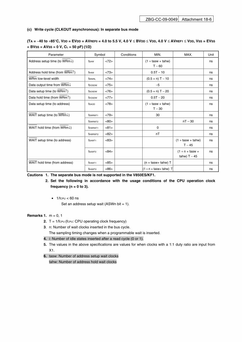
(c) Write cycle (CLKOUT asynchronous): In separate bus mode
(TA = −40 to +85°C, VDD = EVDD = AVREF0 = 4.0 to 5.5 V, 4.0 V ≤ BVDD ≤ VDD, 4.0 V ≤ AVREF1 ≤ VDD, VSS = EVSS
= BVSS = AVSS = 0 V, CL = 50 pF) (1/2)
Parameter Symbol Conditions MIN. MAX. Unit
Address setup time (to WRm↓) tSAW <72> (1 + tasw + tahw)
T − 60
ns
Address hold time (from WRm↑) tHAW <73> 0.5T − 10 ns
WRm low-level width tWWRL <74> (0.5 + n) T − 10 ns
Data output time from WRm↓ tDOSDW <75> −5 ns
Data setup time (to WRm↑) tSOSDW <76> (0.5 + n) T − 20 ns
Data hold time (from WRm↑) tHOSDW <77> 0.5T − 20 ns
Data setup time (to address) tSAOD <78> (1 + tasw + tahw)
T − 30
ns
tSWRWT1 <79> 30 ns WAIT setup time (to WRm↓)
tSWRWT2 <80> nT − 30 ns
tHWRWT1 <81> 0 ns WAIT hold time (from WRm↓)
tHWRWT2 <82> nT ns
tSAWT1 <83> (1 + tasw + tahw)
T − 45
ns WAIT setup time (to address)
tSAWT2 <84> (1 + n + tasw +
tahw) T − 45
ns
tHAWT1 <85> (n + tasw+ tahw) T ns WAIT hold time (from address)
tHAWT2 <86> (1 + n + tasw+ tahw) T ns
Cautions 1. The separate bus mode is not supported in the V850ES/KF1.
2. Set the following in accordance with the usage conditions of the CPU operation clock
frequency (n = 0 to 3).
• 1/fCPU < 60 ns
Set an address setup wait (ASWn bit = 1).
Remarks 1. m = 0, 1
2. T = 1/fCPU (fCPU: CPU operating clock frequency)
3. n: Number of wait clocks inserted in the bus cycle.
The sampling timing changes when a programmable wait is inserted.
4. i: Number of idle states inserted after a read cycle (0 or 1).
5. The values in the above specifications are values for when clocks with a 1:1 duty ratio are input from
X1.
6. tasw: Number of address setup wait clocks
tahw: Number of address hold wait clocks
ZBG-CC-09-0049 Attachment 18-7
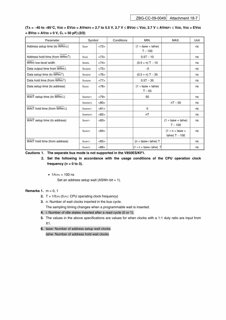
(TA = −40 to +85°C, VDD = EVDD = AVREF0 = 2.7 to 5.5 V, 2.7 V ≤ BVDD ≤ VDD, 2.7 V ≤ AVREF1 ≤ VDD, VSS = EVSS
= BVSS = AVSS = 0 V, CL = 50 pF) (2/2)
Parameter Symbol Conditions MIN. MAX. Unit
Address setup time (to WRm↓) tSAW <72> (1 + tasw + tahw)
T − 100
ns
Address hold time (from WRm↑) tHAW <73> 0.5T − 10 ns
WRm low-level width tWWRL <74> (0.5 + n) T − 10 ns
Data output time from WRm↓ tDOSDW <75> −5 ns
Data setup time (to WRm↑) tSOSDW <76> (0.5 + n) T − 35 ns
Data hold time (from WRm↑) tHOSDW <77> 0.5T − 35 ns
Data setup time (to address) tSAOD <78> (1 + tasw + tahw)
T − 55
ns
tSWRWT1 <79> 50 ns WAIT setup time (to WRm↓)
tSWRWT2 <80> nT − 50 ns
tHWRWT1 <81> 0 ns WAIT hold time (from WRm↓)
tHWRWT2 <82> nT ns
tSAWT1 <83> (1 + tasw + tahw)
T − 100
ns WAIT setup time (to address)
tSAWT2 <84> (1 + n + tasw +
tahw) T − 100
ns
tHAWT1 <85> (n + tasw+ tahw) T ns WAIT hold time (from address)
tHAWT2 <86> (1 + n + tasw+ tahw) T ns
Cautions 1. The separate bus mode is not supported in the V850ES/KF1.
2. Set the following in accordance with the usage conditions of the CPU operation clock
frequency (n = 0 to 3).
• 1/fCPU < 100 ns
Set an address setup wait (ASWn bit = 1).
Remarks 1. m = 0, 1
2. T = 1/fCPU (fCPU: CPU operating clock frequency)
3. n: Number of wait clocks inserted in the bus cycle.
The sampling timing changes when a programmable wait is inserted.
4. i: Number of idle states inserted after a read cycle (0 or 1).
5. The values in the above specifications are values for when clocks with a 1:1 duty ratio are input from
X1.
6. tasw: Number of address setup wait clocks
tahw: Number of address hold wait clocks
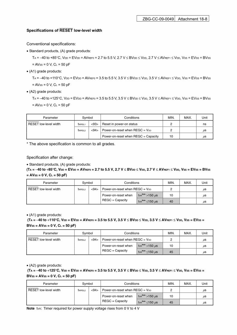
ZBG-CC-09-0049 Attachment 18-8
Specifications of RESET low-level width
Conventional specifications:
• Standard products, (A) grade products:
TA = −40 to +85°C, VDD = EVDD = AVREF0 = 2.7 to 5.5 V, 2.7 V ≤ BVDD ≤ VDD, 2.7 V ≤ AVREF1 ≤ VDD, VSS = EVSS = BVSS
= AVSS = 0 V, CL = 50 pF
• (A1) grade products:
TA = −40 to +110°C, VDD = EVDD = AVREF0 = 3.5 to 5.5 V, 3.5 V ≤ BVDD ≤ VDD, 3.5 V ≤ AVREF1 ≤ VDD, VSS = EVSS = BVSS
= AVSS = 0 V, CL = 50 pF
• (A2) grade products:
TA = −40 to +125°C, VDD = EVDD = AVREF0 = 3.5 to 5.5 V, 3.5 V ≤ BVDD ≤ VDD, 3.5 V ≤ AVREF1 ≤ VDD, VSS = EVSS = BVSS
= AVSS = 0 V, CL = 50 pF
Parameter Symbol Conditions MIN. MAX. Unit
tWRSL1 <93> Reset in power-on status 2 ns
Power-on-reset when REGC = VDD 2 μs
RESET low-level width
tWRSL2 <94>
Power-on-reset when REGC = Capacity 10 μs
* The above specification is common to all grades.
Specification after change:
• Standard products, (A) grade products: (TA = −40 to +85°C, VDD = EVDD = AVREF0 = 2.7 to 5.5 V, 2.7 V ≤ BVDD ≤ VDD, 2.7 V ≤ AVREF1 ≤ VDD, VSS = EVSS = BVSS
= AVSS = 0 V, CL = 50 pF)
Parameter Symbol Conditions MIN. MAX. Unit
Power-on-reset when REGC = VDD 2 μs
tVRNote >150 μs 10 μs
RESET low-level width tWRSL2 <94>
Power-on-reset when
REGC = Capacity tVRNote ≤150 μs 40 μs
• (A1) grade products: (TA = −40 to +110°C, VDD = EVDD = AVREF0 = 3.5 to 5.5 V, 3.5 V ≤ BVDD ≤ VDD, 3.5 V ≤ AVREF1 ≤ VDD, VSS = EVSS =
BVSS = AVSS = 0 V, CL = 50 pF)
Parameter Symbol Conditions MIN. MAX. Unit
Power-on-reset when REGC = VDD 2 μs
tVRNote >150 μs 10 μs
RESET low-level width tWRSL2 <94>
Power-on-reset when
REGC = Capacity tVRNote ≤150 μs 45 μs
• (A2) grade products: (TA = −40 to +125°C, VDD = EVDD = AVREF0 = 3.5 to 5.5 V, 3.5 V ≤ BVDD ≤ VDD, 3.5 V ≤ AVREF1 ≤ VDD, VSS = EVSS =
BVSS = AVSS = 0 V, CL = 50 pF)
Parameter Symbol Conditions MIN. MAX. Unit
Power-on-reset when REGC = VDD 2 μs
tVRNote >150 μs 10 μs
RESET low-level width tWRSL2 <94>
Power-on-reset when
REGC = Capacity tVRNote ≤150 μs 45 μs
Note tVR: Timer required for power supply voltage rises from 0 V to 4 V
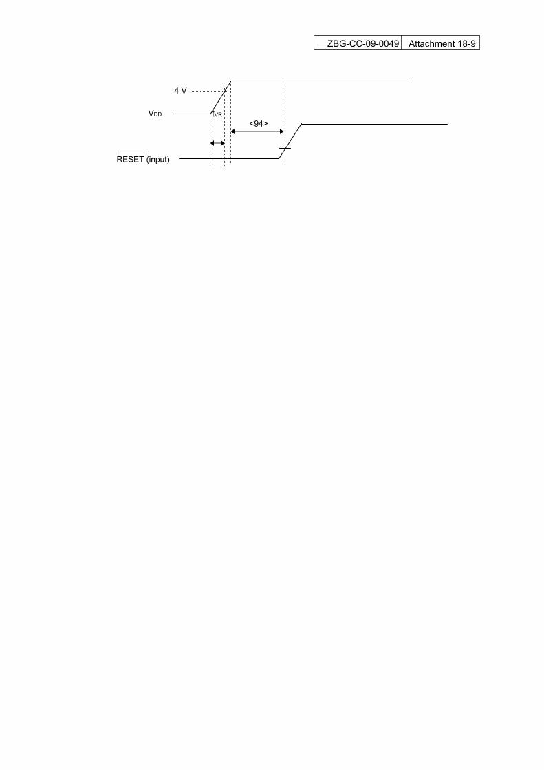
ZBG-CC-09-0049 Attachment 18-9
VDD
RESET (input)
<94>
4 V
tVR
ZBG-CC-09-0049 Attachment 19
Restriction Details No. 1 Restriction on reading buffer RAM when using 3-wire serial interface (CSIA) with automatic
transmit/receive function Description:
If data is written to the buffer RAM and the value is read immediately when using the 3-wire serial
interface (CSIA) with automatic transmit/receive function, the correct value might not be read depending
on the timing.
Workaround:
Before reading the value written to the buffer RAM, wait for 6 fSCKA cycles or longer (serial clock cycles
specified by bits 6 and 7 (CKSAn0, CKSAn1) of CSISn) or write data to another address of the buffer
RAM.
Action:
Regard this item as a usage restriction.
This change will be applied to the 2nd edition of the user’s manuals (U16889E, U16890E, U16891E), as
a caution on use.
ZBG-CC-09-0049 Attachment 20-1
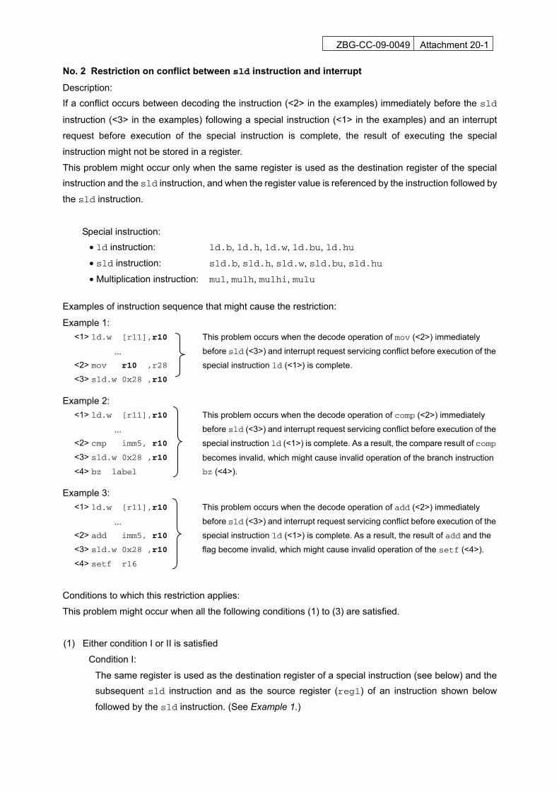
No. 2 Restriction on conflict between sld instruction and interrupt
Description: If a conflict occurs between decoding the instruction (<2> in the examples) immediately before the sld
instruction (<3> in the examples) following a special instruction (<1> in the examples) and an interrupt
request before execution of the special instruction is complete, the result of executing the special
instruction might not be stored in a register.
This problem might occur only when the same register is used as the destination register of the special instruction and the sld instruction, and when the register value is referenced by the instruction followed by
the sld instruction.
Special instruction: • ld instruction: ld.b, ld.h, ld.w, ld.bu, ld.hu
• sld instruction: sld.b, sld.h, sld.w, sld.bu, sld.hu
• Multiplication instruction: mul, mulh, mulhi, mulu
Examples of instruction sequence that might cause the restriction:
Example 1: <1> ld.w [r11],r10
... <2> mov r10 ,r28
<3> sld.w 0x28 ,r10
This problem occurs when the decode operation of mov (<2>) immediately
before sld (<3>) and interrupt request servicing conflict before execution of the
special instruction ld (<1>) is complete.
Example 2:
<1> ld.w [r11],r10
... <2> cmp imm5, r10
<3> sld.w 0x28 ,r10
<4> bz label
This problem occurs when the decode operation of comp (<2>) immediately
before sld (<3>) and interrupt request servicing conflict before execution of the
special instruction ld (<1>) is complete. As a result, the compare result of comp
becomes invalid, which might cause invalid operation of the branch instruction bz (<4>).
Example 3:
<1> ld.w [r11],r10
... <2> add imm5, r10
<3> sld.w 0x28 ,r10 <4> setf r16
This problem occurs when the decode operation of add (<2>) immediately
before sld (<3>) and interrupt request servicing conflict before execution of the
special instruction ld (<1>) is complete. As a result, the result of add and the
flag become invalid, which might cause invalid operation of the setf (<4>).
Conditions to which this restriction applies:
This problem might occur when all the following conditions (1) to (3) are satisfied.
(1) Either condition I or II is satisfied
Condition I:
The same register is used as the destination register of a special instruction (see below) and the subsequent sld instruction and as the source register (reg1) of an instruction shown below
followed by the sld instruction. (See Example 1.)
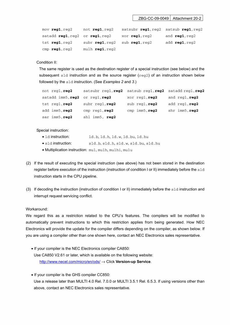
ZBG-CC-09-0049 Attachment 20-2
mov reg1,reg2 not reg1,reg2 satsubr reg1,reg2 satsub reg1,reg2
satadd reg1,reg2 or reg1,reg2 xor reg1,reg2 and reg1,reg2
tst reg1,reg2 subr reg1,reg2 sub reg1,reg2 add reg1,reg2
cmp reg1,reg2 mulh reg1,reg2
Condition II:
The same register is used as the destination register of a special instruction (see below) and the subsequent sld instruction and as the source register (reg2) of an instruction shown below
followed by the sld instruction. (See Examples 2 and 3.)
not reg1,reg2 satsubr reg1,reg2 satsub reg1,reg2 satadd reg1,reg2
satadd imm5,reg2 or reg1,reg2 xor reg1,reg2 and reg1,reg2
tst reg1,reg2 subr reg1,reg2 sub reg1,reg2 add reg1,reg2
add imm5,reg2 cmp reg1,reg2 cmp imm5,reg2 shr imm5,reg2
sar imm5,reg2 shl imm5, reg2
Special instruction: • ld instruction: ld.b, ld.h, ld.w, ld.bu, ld.hu
• sld instruction: sld.b, sld.h, sld.w, sld.bu, sld.hu
• Multiplication instruction: mul, mulh, mulhi, mulu
(2) If the result of executing the special instruction (see above) has not been stored in the destination register before execution of the instruction (instruction of condition I or II) immediately before the sld
instruction starts in the CPU pipeline.
(3) If decoding the instruction (instruction of condition I or II) immediately before the sld instruction and
interrupt request servicing conflict.
Workaround:
We regard this as a restriction related to the CPU’s features. The compilers will be modified to
automatically prevent instructions to which this restriction applies from being generated. How NEC
Electronics will provide the update for the compiler differs depending on the compiler, as shown below. If
you are using a compiler other than one shown here, contact an NEC Electronics sales representative.
• If your compiler is the NEC Electronics compiler CA850:
Use CA850 V2.61 or later, which is available on the following website:
http://www.necel.com/micro/en/ods/ → Click Version-up Service.
• If your compiler is the GHS compiler CC850:
Use a release later than MULTI 4.0 Rel. 7.0.0 or MULTI 3.5.1 Rel. 6.5.3. If using versions other than
above, contact an NEC Electronics sales representative.
ZBG-CC-09-0049 Attachment 21-1
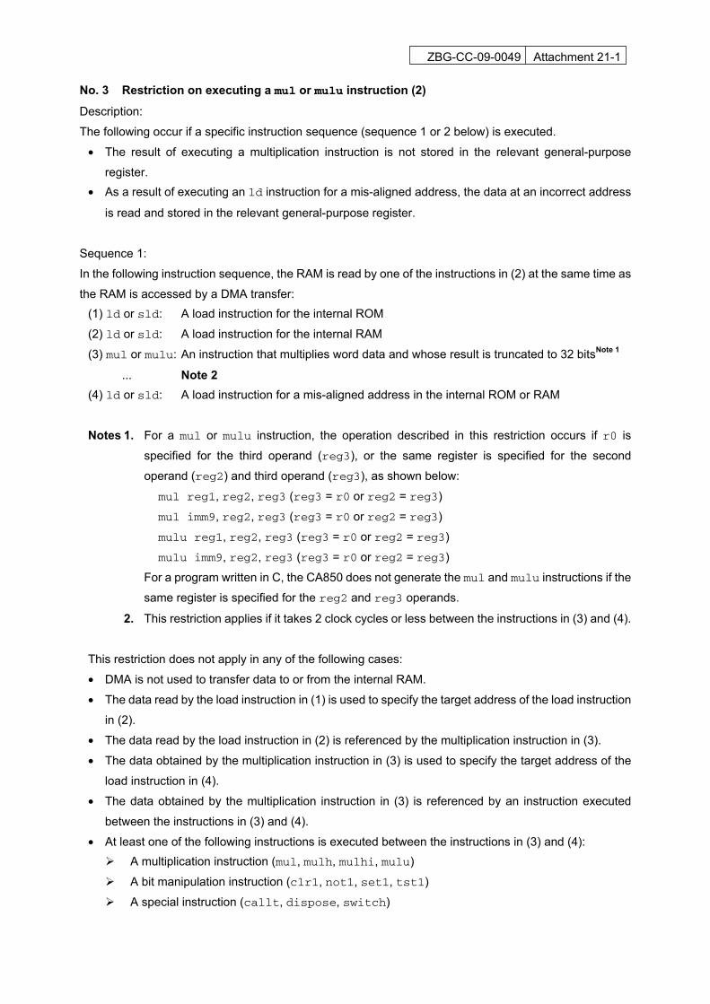
No. 3 Restriction on executing a mul or mulu instruction (2)
Description:
The following occur if a specific instruction sequence (sequence 1 or 2 below) is executed.
• The result of executing a multiplication instruction is not stored in the relevant general-purpose
register. • As a result of executing an ld instruction for a mis-aligned address, the data at an incorrect address
is read and stored in the relevant general-purpose register.
Sequence 1:
In the following instruction sequence, the RAM is read by one of the instructions in (2) at the same time as
the RAM is accessed by a DMA transfer: (1) ld or sld: A load instruction for the internal ROM
(2) ld or sld: A load instruction for the internal RAM
(3) mul or mulu: An instruction that multiplies word data and whose result is truncated to 32 bitsNote 1
... Note 2 (4) ld or sld: A load instruction for a mis-aligned address in the internal ROM or RAM
Notes 1. For a mul or mulu instruction, the operation described in this restriction occurs if r0 is
specified for the third operand (reg3), or the same register is specified for the second
operand (reg2) and third operand (reg3), as shown below:
mul reg1, reg2, reg3 (reg3 = r0 or reg2 = reg3)
mul imm9, reg2, reg3 (reg3 = r0 or reg2 = reg3)
mulu reg1, reg2, reg3 (reg3 = r0 or reg2 = reg3)
mulu imm9, reg2, reg3 (reg3 = r0 or reg2 = reg3)
For a program written in C, the CA850 does not generate the mul and mulu instructions if the
same register is specified for the reg2 and reg3 operands.
2. This restriction applies if it takes 2 clock cycles or less between the instructions in (3) and (4).
This restriction does not apply in any of the following cases:
• DMA is not used to transfer data to or from the internal RAM.
• The data read by the load instruction in (1) is used to specify the target address of the load instruction
in (2).
• The data read by the load instruction in (2) is referenced by the multiplication instruction in (3).
• The data obtained by the multiplication instruction in (3) is used to specify the target address of the
load instruction in (4).
• The data obtained by the multiplication instruction in (3) is referenced by an instruction executed
between the instructions in (3) and (4).
• At least one of the following instructions is executed between the instructions in (3) and (4): A multiplication instruction (mul, mulh, mulhi, mulu)
A bit manipulation instruction (clr1, not1, set1, tst1)
A special instruction (callt, dispose, switch)
ZBG-CC-09-0049 Attachment 21-2
• The instruction in (4) is a load instruction that accesses the memory in bytes (ld.b, ld.bu, sld.b,
or sld.bu).
• The instructions in (1) to (4) are located in an external memory or the internal RAM.
Sequence 2:
In the following instruction sequence, access by the instruction in (1) ends at the same time as the
instruction in (2) accesses the internal RAM: (1) ld or sld: A load instruction for an external memory
... Note 1 (2) ld or sld: A load instruction for the internal RAM
(3) mul or mulu: An instruction that multiplies word data and whose result is truncated to 32 bitsNote 2
... Note 3 (4) ld or sld: A load instruction for a mis-aligned address in the internal ROM or RAM
Notes 1. This restriction applies if a different instruction is executed between the load instructions in (1)
and (2), and the access by the instruction in (1) ends at the same time as the instruction in (2)
accesses the internal RAM. 2. For a mul or mulu instruction, the operation described in this restriction occurs if r0 is
specified for the third operand (reg3), or the same register is specified for the second
operand (reg2) and third operand (reg3), as shown below: mul reg1, reg2, reg3 (reg3 = r0 or reg2 = reg3)
mul imm9, reg2, reg3 (reg3 = r0 or reg2 = reg3)
mulu reg1, reg2, reg3 (reg3 = r0 or reg2 = reg3)
mulu imm9, reg2, reg3 (reg3 = r0 or reg2 = reg3)
For a program written in C, the CA850 does not generate the mul and mulu instructions if the
same register is specified for the reg2 and reg3 operands.
3. This restriction applies if it takes 2 clock cycles or less between the instructions in (3) and (4).
This restriction does not apply in any of the following cases:
• An external bus is not used.
• The data read by the load instruction in (1) is used to specify the target address of the load instruction
in (2).
• The data read by the load instruction in (1) is referenced by an instruction executed between the
instructions in (1) and (2).
• The data read by the load instruction in (2) is referenced by the multiplication instruction in (3).
• The data obtained by the multiplication instruction in (3) is used to specify the target address of the
load instruction in (4).
• The data obtained by the multiplication instruction in (3) is referenced by an instruction executed
between the instructions in (3) and (4).
ZBG-CC-09-0049 Attachment 21-3
• At least one of the following instructions is executed between the instructions in (3) and (4): A multiplication instruction (mul, mulh, mulhi, mulu)
A bit manipulation instruction (clr1, not1, set1, tst1)
A special instruction (callt, dispose, switch)
• The instruction in (4) is a load instruction that accesses the memory in bytes (ld.b, ld.bu, sld.b,
or sld.bu).
• The instructions in (1) to (4) are located in an external memory or the internal RAM.
Workaround:
We regard this as a restriction related to the CPU’s features and do not intend to correct the
microcontroller. Instead, the CA850 compiler will be modified to automatically prevent instructions to
which this restriction applies from being generated. This workaround does not work for instructions in
assembly code, so the CA850 outputs a message for such instructions. How NEC Electronics will
provide the update for the compiler is shown below.
If you are using another compiler, contact an NEC Electronics sales representative.
• If your compiler is the NEC Electronics compiler CA850:
The CA850 will be upgraded to add the above workaround.
The following table shows the version and release schedule for the C compiler package CA850, and
the software package SP850 that includes the CA850.
Product Name Current CA850
Version
Version of CA850
After Upgrade
Language Release Schedule
Japanese November 9, 2009 SP850,
CA850
V3.40 V3.42
English November 9, 2009
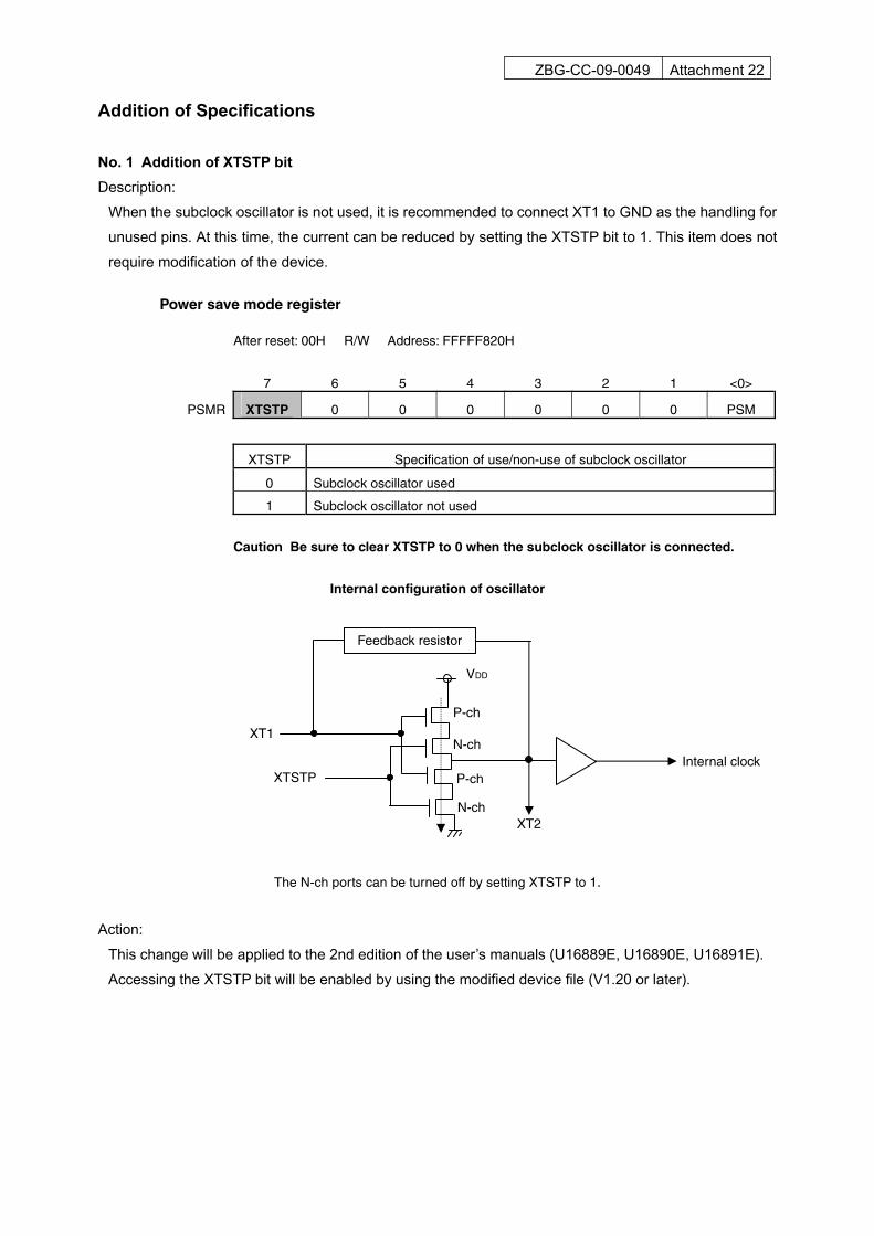
ZBG-CC-09-0049 Attachment 22
Addition of Specifications
No. 1 Addition of XTSTP bit Description:
When the subclock oscillator is not used, it is recommended to connect XT1 to GND as the handling for
unused pins. At this time, the current can be reduced by setting the XTSTP bit to 1. This item does not
require modification of the device.
Power save mode register
After reset: 00H R/W Address: FFFFF820H
7 6 5 4 3 2 1 <0>
PSMR XTSTP 0 0 0 0 0 0 PSM
XTSTP Specification of use/non-use of subclock oscillator
0 Subclock oscillator used
1 Subclock oscillator not used
Caution Be sure to clear XTSTP to 0 when the subclock oscillator is connected.
Internal configuration of oscillator
The N-ch ports can be turned off by setting XTSTP to 1.
Action:
This change will be applied to the 2nd edition of the user’s manuals (U16889E, U16890E, U16891E).
Accessing the XTSTP bit will be enabled by using the modified device file (V1.20 or later).
XT1
XTSTP Internal clock
P-ch
N-ch
P-ch
N-ch XT2
Feedback resistor
VDD