MSP430FG42x0 Mixed Signal Microcontroller (Rev. A) MIXED SIGNAL MICROCONTROLLER SLAS556A − JULY...
68
MSP430FG42x0 MIXED SIGNAL MICROCONTROLLER SLAS556A - JULY 2007 - REVISED AUGUST 2007 1 POST OFFICE BOX 655303 • DALLAS, TEXAS 75265 D Low Supply-Voltage Range, 1.8 V to 3.6 V D Ultralow-Power Consumption: Active Mode: 250 μA at 1 MHz, 2.2 V Standby Mode: 1.1 μA Off Mode (RAM Retention): 0.1 μA D Five Power Saving Modes D Wake-Up From Standby Mode in Less Than 6 μs D 16-Bit RISC Architecture, 125-ns Instruction Cycle Time D 16-Bit Sigma-Delta A/D Converter With Internal Reference and Five Differential Analog Inputs D 12-Bit D/A Converter D Two Configurable Operational Amplifiers D 16-Bit Timer_A With Three Capture/Compare Registers D Brownout Detector D Bootstrap Loader D Serial Onboard Programming, No External Programming Voltage Needed Programmable Code Protection by Security Fuse D Integrated LCD Driver With Contrast Control for up to 56 Segments D MSP430FG42x0 Family Members Include: MSP430FG4250: 16KB+256B Flash Memory 256B RAM MSP430FG4260: 24KB+256B Flash Memory 256B RAM MSP430FG4270: 32KB+256B Flash Memory 256B RAM D For Complete Module Descriptions, See MSP430x4xx Family User’s Guide, Literature Number SLAU056 D For Additional Device Information, See MSP430FG42x0 Device Erratasheet, Literature Number SLAZ038 description The Texas Instruments MSP430 family of ultralow-power microcontrollers consist of several devices featuring different sets of peripherals targeted for various applications. The architecture, combined with five low-power modes, is optimized to achieve extended battery life in portable measurement applications. The device features a powerful 16-bit RISC CPU, 16-bit registers, and constant generators that contribute to maximum code efficiency. The digitally controlled oscillator (DCO) allows wake-up from low-power modes to active mode in less than 6 μs. The MSP430FG42x0 is a microcontroller configuration with a 16-bit timer, a high-performance 16-bit sigma-delta A/D converter, 12-bit D/A converter, two configurable operational amplifiers, 32 I/O pins, and a liquid crystal display driver. Typical applications for this device include analog and digital sensor systems, digital motor control, remote controls, thermostats, digital timers, hand-held meters, etc. AVAILABLE OPTIONS PACKAGED DEVICES T A PLASTIC 48-PIN SSOP (DL) PLASTIC 48-PIN QFN (RGZ) MSP430FG4250IDL MSP430FG4250IRGZ -40°C to 85°C MSP430FG4260IDL MSP430FG4260IRGZ 40 C to 85 C MSP430FG4270IDL MSP430FG4270IRGZ This integrated circuit can be damaged by ESD. Texas Instruments recommends that all integrated circuits be handled with appropriate precautions. Failure to observe proper handling and installation procedures can cause damage. ESD damage can range from subtle performance degradation to complete device failure. Precision integrated circuits may be more susceptible to damage because very small parametric changes could cause the device not to meet its published specifications. These devices have limited built-in ESD protection. Copyright © 2007, Texas Instruments Incorporated Please be aware that an important notice concerning availability, standard warranty, and use in critical applications of Texas Instruments semiconductor products and disclaimers thereto appears at the end of this data sheet. PRODUCTION DATA information is current as of publication date. Products conform to specifications per the terms of Texas Instruments standard warranty. Production processing does not necessarily include testing of all parameters.
Transcript of MSP430FG42x0 Mixed Signal Microcontroller (Rev. A) MIXED SIGNAL MICROCONTROLLER SLAS556A − JULY...
MSP430FG42x0MIXED SIGNAL MICROCONTROLLER
SLAS556A − JULY 2007 − REVISED AUGUST 2007
1POST OFFICE BOX 655303 • DALLAS, TEXAS 75265
� Low Supply-Voltage Range, 1.8 V to 3.6 V
� Ultralow-Power Consumption:Active Mode: 250 μA at 1 MHz, 2.2 VStandby Mode: 1.1 μAOff Mode (RAM Retention): 0.1 μA
� Five Power Saving Modes
� Wake-Up From Standby Mode in LessThan 6 μs
� 16-Bit RISC Architecture,125-ns Instruction Cycle Time
� 16-Bit Sigma-Delta A/D Converter WithInternal Reference and Five DifferentialAnalog Inputs
� 12-Bit D/A Converter
� Two Configurable Operational Amplifiers
� 16-Bit Timer_A With ThreeCapture/Compare Registers
� Brownout Detector
� Bootstrap Loader
� Serial Onboard Programming,No External Programming Voltage NeededProgrammable Code Protection by SecurityFuse
� Integrated LCD Driver With ContrastControl for up to 56 Segments
� MSP430FG42x0 Family Members Include:MSP430FG4250: 16KB+256B Flash Memory
256B RAMMSP430FG4260: 24KB+256B Flash Memory
256B RAMMSP430FG4270: 32KB+256B Flash Memory
256B RAM
� For Complete Module Descriptions, SeeMSP430x4xx Family User’s Guide,Literature Number SLAU056
� For Additional Device Information, SeeMSP430FG42x0 Device Erratasheet,Literature Number SLAZ038
description
The Texas Instruments MSP430 family of ultralow-power microcontrollers consist of several devices featuringdifferent sets of peripherals targeted for various applications. The architecture, combined with five low-powermodes, is optimized to achieve extended battery life in portable measurement applications. The device featuresa powerful 16-bit RISC CPU, 16-bit registers, and constant generators that contribute to maximum codeefficiency. The digitally controlled oscillator (DCO) allows wake-up from low-power modes to active mode in lessthan 6 μs.
The MSP430FG42x0 is a microcontroller configuration with a 16-bit timer, a high-performance 16-bitsigma-delta A/D converter, 12-bit D/A converter, two configurable operational amplifiers, 32 I/O pins, and a liquidcrystal display driver.
Typical applications for this device include analog and digital sensor systems, digital motor control, remotecontrols, thermostats, digital timers, hand-held meters, etc.
AVAILABLE OPTIONS
PACKAGED DEVICES
TA PLASTIC 48-PIN SSOP(DL)
PLASTIC 48-PIN QFN(RGZ)
MSP430FG4250IDL MSP430FG4250IRGZ
−40°C to 85°C MSP430FG4260IDL MSP430FG4260IRGZ40 C to 85 C
MSP430FG4270IDL MSP430FG4270IRGZ
This integrated circuit can be damaged by ESD. Texas Instruments recommends that all integrated circuits be handled withappropriate precautions. Failure to observe proper handling and installation procedures can cause damage. ESD damage can rangefrom subtle performance degradation to complete device failure. Precision integrated circuits may be more susceptible to damagebecause very small parametric changes could cause the device not to meet its published specifications. These devices have limitedbuilt-in ESD protection.
Copyright © 2007, Texas Instruments Incorporated
Please be aware that an important notice concerning availability, standard warranty, and use in critical applications ofTexas Instruments semiconductor products and disclaimers thereto appears at the end of this data sheet.
PRODUCTION DATA information is current as of publication date.Products conform to specifications per the terms of Texas Instrumentsstandard warranty. Production processing does not necessarily includetesting of all parameters.
MSP430FG42x0MIXED SIGNAL MICROCONTROLLER
SLAS556A − JULY 2007 − REVISED AUGUST 2007
2 POST OFFICE BOX 655303 • DALLAS, TEXAS 75265
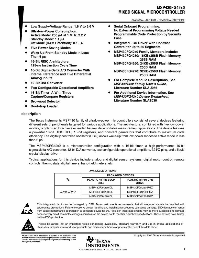
pin designation, DL package
P5.4/COM3P5.3/COM2P5.2/COM1COM0P2.0/S13/SW0CP2.1/S12/SW1CP2.2/S11P2.3/S10P2.4/S9P2.5/S8P2.6/S7P2.7/S6S5P5.7/S4P5.6/S3P5.5/S2P5.0/S1P5.1/S0LCDCAP/R23LCDREF/R13P1.0/TA0P1.1/TA0/MCLKP1.2/TA1/A4−P1.3/TA2/A4+
TDO/TDITDI/TCLK
TMSTCK
RST/NMIDVCC
DVSS
XINXOUTAVSSAVCC
VREF
P6.0/A0+/OA0OP6.1/A0−/OA0FBP6.2/A1+/OA1O
P6.3/A1−/OA1FBP6.4/OA0I1P6.5/OA0I2P6.6/OA1I1P6.7/OA1I2
P1.7/A2+P1.6/A2−/OA0I0
P1.5/TACLK/ACLK/A3+P1.4/A3−/OA1I0/DAC0
DL PACKAGE(TOP VIEW)
MSP430FG42x0IDL
48474645444342414039383736353433
123456789101112131415161718192021222324
3231302928272625
MSP430FG42x0MIXED SIGNAL MICROCONTROLLER
SLAS556A − JULY 2007 − REVISED AUGUST 2007
3POST OFFICE BOX 655303 • DALLAS, TEXAS 75265
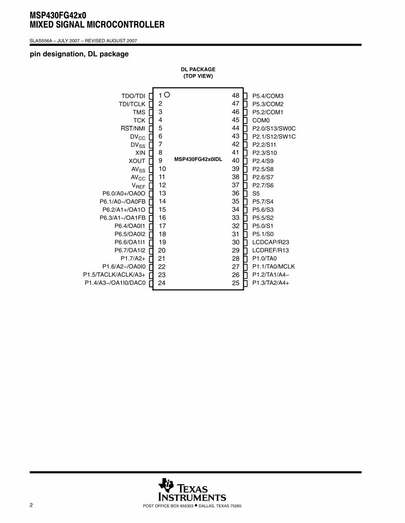
pin designation, RGZ package
1
2
3
4
2514
47
5
6
7
8
9
10
11
1215 16 17 18 19 20 21 22 23
26
27
28
29
30
31
32
33
34
35
3646 45 44 43 42 41 40 39 38DVSS
XIN
XOUT
AVCC
AVSS
VREF
P6.0/A0+/OA0O
P6.1/A0−/OA0FB
P6.2/A1+/OA1O
P6.3/A1−/OA1FB
P6.4/OA0I1
P6.5/OA0I2
P2.2/S11
P2.3/S10
P2.4/S9
P2.5/S8
P2.6/S7
P2.7/S6
S5
P5.7/S4
P5.6/S3
P5.5/S2
P5.0/S1
P5.1/S0
MSP430FG42x0IRGZ
P6.
6/O
A1I
1
P6.
7/O
A1I
2
P1.
7/A
2+
P1.
5/TA
CLK
/AC
LK/A
3+
P1.
6/A
2−/O
A0I
0
P1.
4/A
3−/O
A1I
0/D
AC
0
P1.
3/TA
2/A
4+
P1.
2/TA
1/A
4−
P1.
1/TA
0/M
CLK
P1.
0/TA
0
LCD
RE
F/R
13
LCD
CA
P/R
23
DV
CC
RS
T/N
MI
TC
K
TM
S
TD
I/TC
LK
TD
O/T
DI
P5.
4/C
OM
3
P5.
3/C
OM
2
P5.
2/C
OM
1
CO
M0
P2.
0/S
13/S
W0C
P2.
1/S
12/S
W1C
RGZ PACKAGE(TOP VIEW)
MSP430FG42x0MIXED SIGNAL MICROCONTROLLER
SLAS556A − JULY 2007 − REVISED AUGUST 2007
4 POST OFFICE BOX 655303 • DALLAS, TEXAS 75265
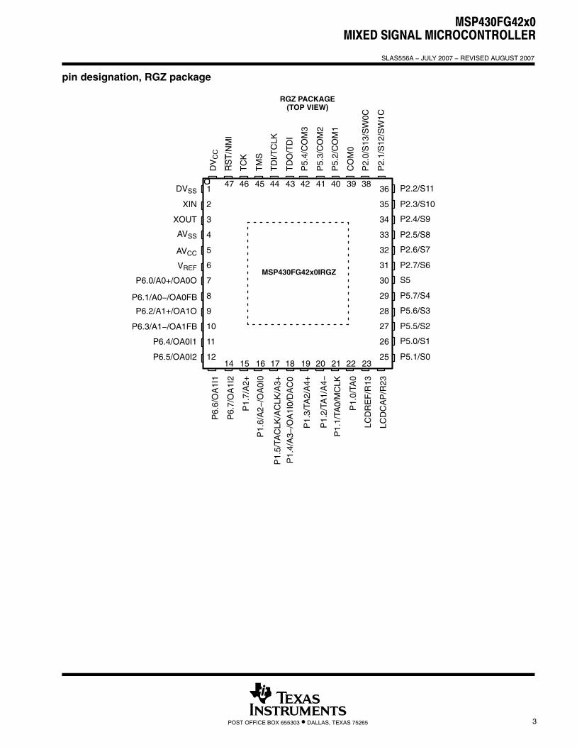
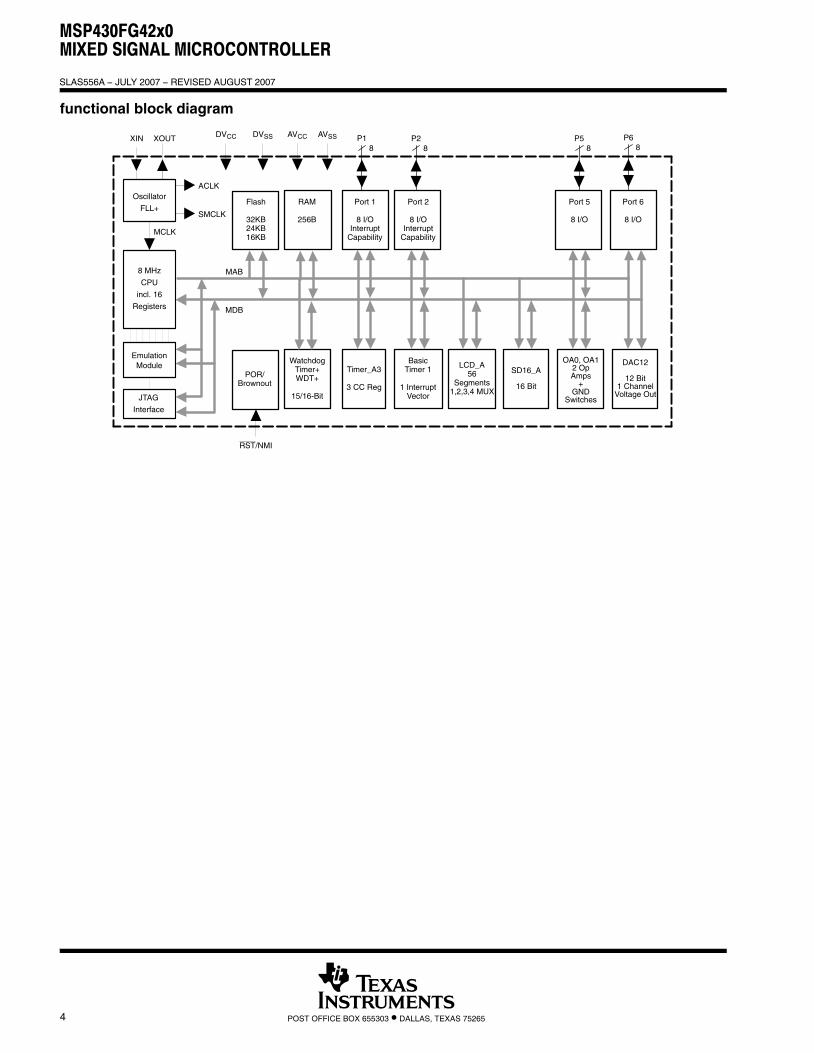
functional block diagram
DVCC DVSS AVCC AVSS
RST/NMI
P2
Flash
32KB24KB16KB
RAM
256B
WatchdogTimer+WDT+
15/16-Bit
Port 2
8 I/OInterrupt
Capability
POR/Brownout
BasicTimer 1
1 InterruptVector
LCD_A56
Segments1,2,3,4 MUX
8
MCLK
XOUT
JTAG
Interface
XIN
SMCLK
ACLK
MDB
MAB
EmulationModule
P1
Port 1
8 I/OInterrupt
Capability
8
SD16_A
16 Bit
Oscillator
FLL+
8 MHz
CPU
incl. 16
Registers
P5
Port 5
8 I/O
8P6
Port 6
8 I/O
8
Timer_A3
3 CC Reg
DAC12
12 Bit1 Channel
Voltage Out
OA0, OA12 OpAmps
+GND
Switches
MSP430FG42x0MIXED SIGNAL MICROCONTROLLER
SLAS556A − JULY 2007 − REVISED AUGUST 2007
5POST OFFICE BOX 655303 • DALLAS, TEXAS 75265
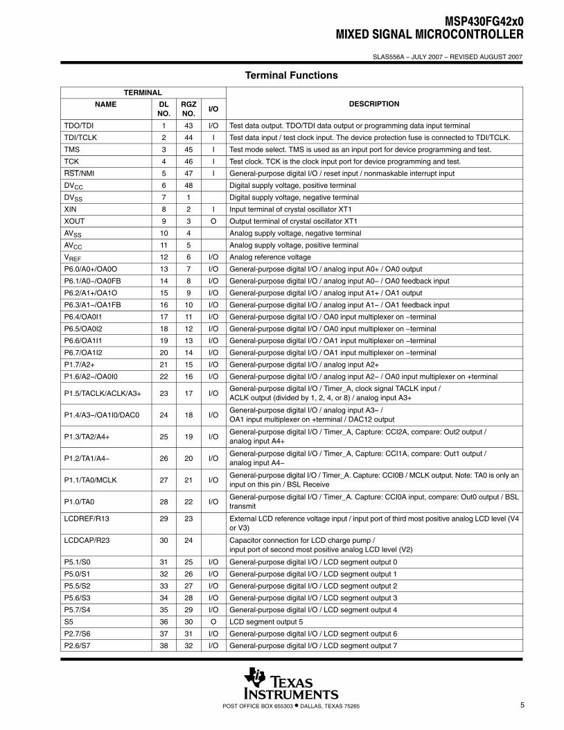
Terminal Functions
TERMINAL
NAME DLNO.
RGZNO.
I/ODESCRIPTION
TDO/TDI 1 43 I/O Test data output. TDO/TDI data output or programming data input terminal
TDI/TCLK 2 44 I Test data input / test clock input. The device protection fuse is connected to TDI/TCLK.
TMS 3 45 I Test mode select. TMS is used as an input port for device programming and test.
TCK 4 46 I Test clock. TCK is the clock input port for device programming and test.
RST/NMI 5 47 I General-purpose digital I/O / reset input / nonmaskable interrupt input
DVCC 6 48 Digital supply voltage, positive terminal
DVSS 7 1 Digital supply voltage, negative terminal
XIN 8 2 I Input terminal of crystal oscillator XT1
XOUT 9 3 O Output terminal of crystal oscillator XT1
AVSS 10 4 Analog supply voltage, negative terminal
AVCC 11 5 Analog supply voltage, positive terminal
VREF 12 6 I/O Analog reference voltage
P6.0/A0+/OA0O 13 7 I/O General-purpose digital I/O / analog input A0+ / OA0 output
P6.1/A0−/OA0FB 14 8 I/O General-purpose digital I/O / analog input A0− / OA0 feedback input
P6.2/A1+/OA1O 15 9 I/O General-purpose digital I/O / analog input A1+ / OA1 output
P6.3/A1−/OA1FB 16 10 I/O General-purpose digital I/O / analog input A1− / OA1 feedback input
P6.4/OA0I1 17 11 I/O General-purpose digital I/O / OA0 input multiplexer on −terminal
P6.5/OA0I2 18 12 I/O General-purpose digital I/O / OA0 input multiplexer on −terminal
P6.6/OA1I1 19 13 I/O General-purpose digital I/O / OA1 input multiplexer on −terminal
P6.7/OA1I2 20 14 I/O General-purpose digital I/O / OA1 input multiplexer on −terminal
P1.7/A2+ 21 15 I/O General-purpose digital I/O / analog input A2+
P1.6/A2−/OA0I0 22 16 I/O General-purpose digital I/O / analog input A2− / OA0 input multiplexer on +terminal
P1.5/TACLK/ACLK/A3+ 23 17 I/OGeneral-purpose digital I/O / Timer_A, clock signal TACLK input / ACLK output (divided by 1, 2, 4, or 8) / analog input A3+
P1.4/A3−/OA1I0/DAC0 24 18 I/OGeneral-purpose digital I/O / analog input A3− / OA1 input multiplexer on +terminal / DAC12 output
P1.3/TA2/A4+ 25 19 I/OGeneral-purpose digital I/O / Timer_A, Capture: CCI2A, compare: Out2 output / analog input A4+
P1.2/TA1/A4− 26 20 I/OGeneral-purpose digital I/O / Timer_A, Capture: CCI1A, compare: Out1 output / analog input A4−
P1.1/TA0/MCLK 27 21 I/OGeneral-purpose digital I/O / Timer_A. Capture: CCI0B / MCLK output. Note: TA0 is only aninput on this pin / BSL Receive
P1.0/TA0 28 22 I/OGeneral-purpose digital I/O / Timer_A. Capture: CCI0A input, compare: Out0 output / BSLtransmit
LCDREF/R13 29 23 External LCD reference voltage input / input port of third most positive analog LCD level (V4or V3)
LCDCAP/R23 30 24 Capacitor connection for LCD charge pump / input port of second most positive analog LCD level (V2)
P5.1/S0 31 25 I/O General-purpose digital I/O / LCD segment output 0
P5.0/S1 32 26 I/O General-purpose digital I/O / LCD segment output 1
P5.5/S2 33 27 I/O General-purpose digital I/O / LCD segment output 2
P5.6/S3 34 28 I/O General-purpose digital I/O / LCD segment output 3
P5.7/S4 35 29 I/O General-purpose digital I/O / LCD segment output 4
S5 36 30 O LCD segment output 5
P2.7/S6 37 31 I/O General-purpose digital I/O / LCD segment output 6
P2.6/S7 38 32 I/O General-purpose digital I/O / LCD segment output 7
MSP430FG42x0MIXED SIGNAL MICROCONTROLLER
SLAS556A − JULY 2007 − REVISED AUGUST 2007
6 POST OFFICE BOX 655303 • DALLAS, TEXAS 75265
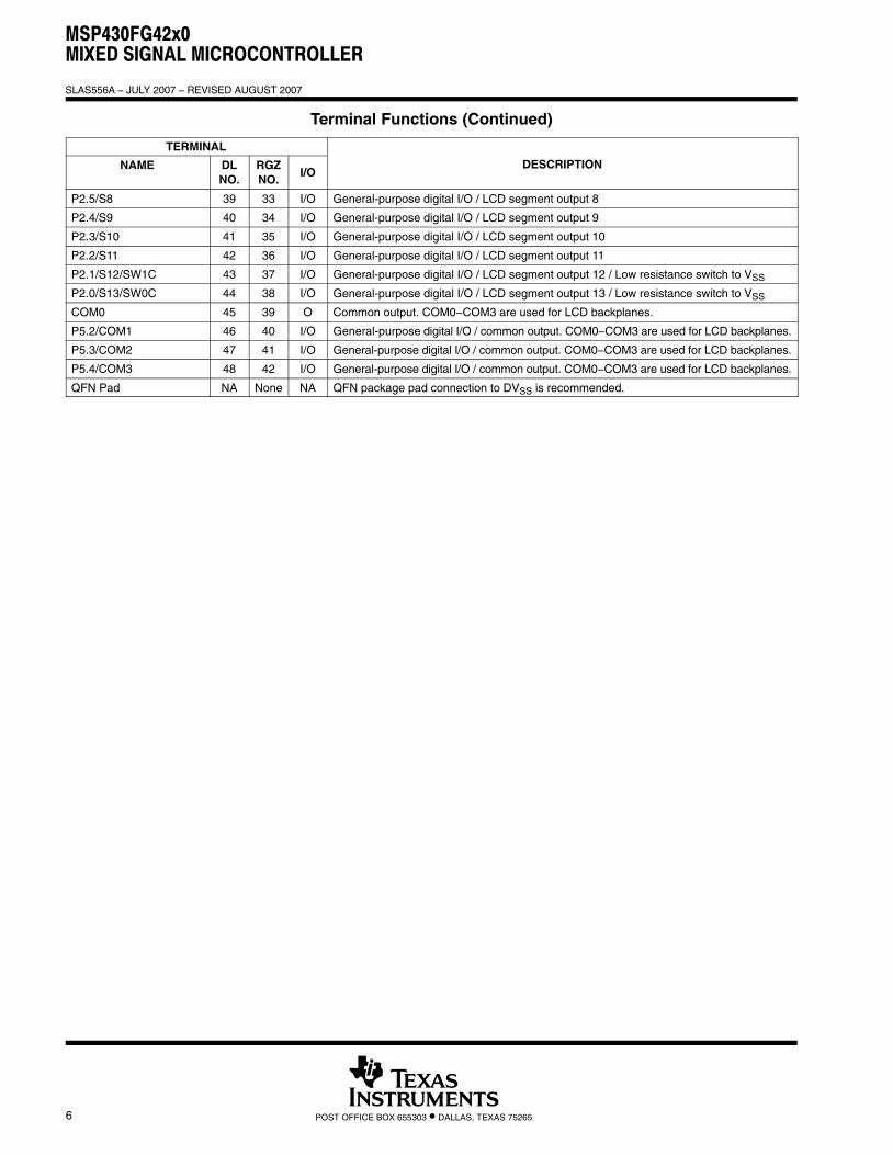
Terminal Functions (Continued)
TERMINAL
NAME DLNO.
RGZNO.
I/ODESCRIPTION
P2.5/S8 39 33 I/O General-purpose digital I/O / LCD segment output 8
P2.4/S9 40 34 I/O General-purpose digital I/O / LCD segment output 9
P2.3/S10 41 35 I/O General-purpose digital I/O / LCD segment output 10
P2.2/S11 42 36 I/O General-purpose digital I/O / LCD segment output 11
P2.1/S12/SW1C 43 37 I/O General-purpose digital I/O / LCD segment output 12 / Low resistance switch to VSS
P2.0/S13/SW0C 44 38 I/O General-purpose digital I/O / LCD segment output 13 / Low resistance switch to VSS
COM0 45 39 O Common output. COM0−COM3 are used for LCD backplanes.
P5.2/COM1 46 40 I/O General-purpose digital I/O / common output. COM0−COM3 are used for LCD backplanes.
P5.3/COM2 47 41 I/O General-purpose digital I/O / common output. COM0−COM3 are used for LCD backplanes.
P5.4/COM3 48 42 I/O General-purpose digital I/O / common output. COM0−COM3 are used for LCD backplanes.
QFN Pad NA None NA QFN package pad connection to DVSS is recommended.
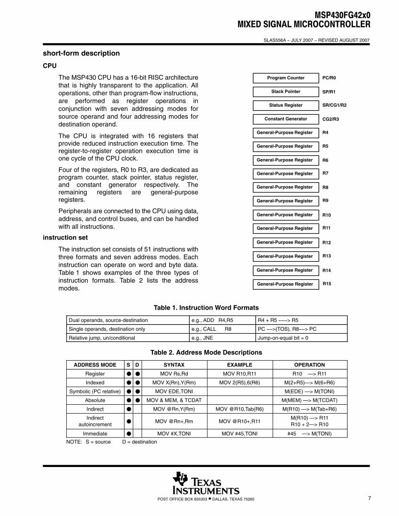
General-Purpose Register
Program Counter
Stack Pointer
Status Register
Constant Generator
General-Purpose Register
General-Purpose Register
General-Purpose Register
PC/R0
SP/R1
SR/CG1/R2
CG2/R3
R4
R5
R12
R13
General-Purpose Register
General-Purpose Register
R6
R7
General-Purpose Register
General-Purpose Register
R8
R9
General-Purpose Register
General-Purpose Register
R10
R11
General-Purpose Register
General-Purpose Register
R14
R15
MSP430FG42x0MIXED SIGNAL MICROCONTROLLER
SLAS556A − JULY 2007 − REVISED AUGUST 2007
7POST OFFICE BOX 655303 • DALLAS, TEXAS 75265
short-form description
CPU
The MSP430 CPU has a 16-bit RISC architecturethat is highly transparent to the application. Alloperations, other than program-flow instructions,are performed as register operations inconjunction with seven addressing modes forsource operand and four addressing modes fordestination operand.
The CPU is integrated with 16 registers thatprovide reduced instruction execution time. Theregister-to-register operation execution time isone cycle of the CPU clock.
Four of the registers, R0 to R3, are dedicated asprogram counter, stack pointer, status register,and constant generator respectively. Theremaining registers are general-purposeregisters.
Peripherals are connected to the CPU using data,address, and control buses, and can be handledwith all instructions.
instruction set
The instruction set consists of 51 instructions withthree formats and seven address modes. Eachinstruction can operate on word and byte data.Table 1 shows examples of the three types ofinstruction formats. Table 2 lists the addressmodes.
Table 1. Instruction Word Formats
Dual operands, source-destination e.g., ADD R4,R5 R4 + R5 −−−> R5
Single operands, destination only e.g., CALL R8 PC −−>(TOS), R8−−> PC
Relative jump, un/conditional e.g., JNE Jump-on-equal bit = 0
Table 2. Address Mode Descriptions
ADDRESS MODE S D SYNTAX EXAMPLE OPERATION
Register � � MOV Rs,Rd MOV R10,R11 R10 —> R11
Indexed � � MOV X(Rn),Y(Rm) MOV 2(R5),6(R6) M(2+R5)—> M(6+R6)
Symbolic (PC relative) � � MOV EDE,TONI M(EDE) —> M(TONI)
Absolute � � MOV & MEM, & TCDAT M(MEM) —> M(TCDAT)
Indirect � MOV @Rn,Y(Rm) MOV @R10,Tab(R6) M(R10) —> M(Tab+R6)
Indirectautoincrement
� MOV @Rn+,Rm MOV @R10+,R11M(R10) —> R11R10 + 2—> R10
Immediate � MOV #X,TONI MOV #45,TONI #45 —> M(TONI)
NOTE: S = source D = destination
MSP430FG42x0MIXED SIGNAL MICROCONTROLLER
SLAS556A − JULY 2007 − REVISED AUGUST 2007
8 POST OFFICE BOX 655303 • DALLAS, TEXAS 75265
operating modes
The MSP430 has one active mode and five software selectable low-power modes of operation. An interruptevent can wake up the device from any of the five low-power modes, service the request, and restore back tothe low-power mode on return from the interrupt program.
The following six operating modes can be configured by software:
� Active mode (AM)
− All clocks are active
� Low-power mode 0 (LPM0)
− CPU is disabledACLK and SMCLK remain active, MCLK is available to modulesFLL+ loop control remains active
� Low-power mode 1 (LPM1)
− CPU is disabledACLK and SMCLK remain active, MCLK is available to modulesFLL+ loop control is disabled
� Low-power mode 2 (LPM2)
− CPU is disabledMCLK, FLL+ loop control, and DCOCLK are disabledDCO’s dc-generator remains enabledACLK remains active
� Low-power mode 3 (LPM3)
− CPU is disabledMCLK, FLL+ loop control, and DCOCLK are disabledDCO’s dc-generator is disabledACLK remains active
� Low-power mode 4 (LPM4)
− CPU is disabledACLK is disabledMCLK, FLL+ loop control, and DCOCLK are disabledDCO’s dc-generator is disabledCrystal oscillator is stopped
MSP430FG42x0MIXED SIGNAL MICROCONTROLLER
SLAS556A − JULY 2007 − REVISED AUGUST 2007
9POST OFFICE BOX 655303 • DALLAS, TEXAS 75265
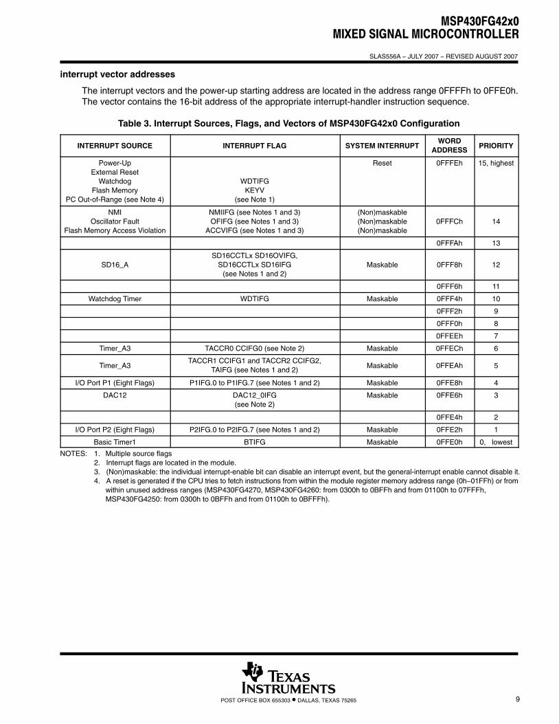
interrupt vector addresses
The interrupt vectors and the power-up starting address are located in the address range 0FFFFh to 0FFE0h.The vector contains the 16-bit address of the appropriate interrupt-handler instruction sequence.
Table 3. Interrupt Sources, Flags, and Vectors of MSP430FG42x0 Configuration
INTERRUPT SOURCE INTERRUPT FLAG SYSTEM INTERRUPTWORD
ADDRESS PRIORITY
Power-UpExternal Reset
WatchdogFlash Memory
PC Out-of-Range (see Note 4)
WDTIFGKEYV
(see Note 1)
Reset 0FFFEh 15, highest
NMIOscillator Fault
Flash Memory Access Violation
NMIIFG (see Notes 1 and 3)OFIFG (see Notes 1 and 3)
ACCVIFG (see Notes 1 and 3)
(Non)maskable(Non)maskable(Non)maskable
0FFFCh 14
0FFFAh 13
SD16_ASD16CCTLx SD16OVIFG,
SD16CCTLx SD16IFG(see Notes 1 and 2)
Maskable 0FFF8h 12
0FFF6h 11
Watchdog Timer WDTIFG Maskable 0FFF4h 10
0FFF2h 9
0FFF0h 8
0FFEEh 7
Timer_A3 TACCR0 CCIFG0 (see Note 2) Maskable 0FFECh 6
Timer_A3TACCR1 CCIFG1 and TACCR2 CCIFG2,
TAIFG (see Notes 1 and 2)Maskable 0FFEAh 5
I/O Port P1 (Eight Flags) P1IFG.0 to P1IFG.7 (see Notes 1 and 2) Maskable 0FFE8h 4
DAC12 DAC12_0IFG(see Note 2)
Maskable 0FFE6h 3
0FFE4h 2
I/O Port P2 (Eight Flags) P2IFG.0 to P2IFG.7 (see Notes 1 and 2) Maskable 0FFE2h 1
Basic Timer1 BTIFG Maskable 0FFE0h 0, lowest
NOTES: 1. Multiple source flags2. Interrupt flags are located in the module.3. (Non)maskable: the individual interrupt-enable bit can disable an interrupt event, but the general-interrupt enable cannot disable it.4. A reset is generated if the CPU tries to fetch instructions from within the module register memory address range (0h−01FFh) or from
within unused address ranges (MSP430FG4270, MSP430FG4260: from 0300h to 0BFFh and from 01100h to 07FFFh, MSP430FG4250: from 0300h to 0BFFh and from 01100h to 0BFFFh).
MSP430FG42x0MIXED SIGNAL MICROCONTROLLER
SLAS556A − JULY 2007 − REVISED AUGUST 2007
10 POST OFFICE BOX 655303 • DALLAS, TEXAS 75265
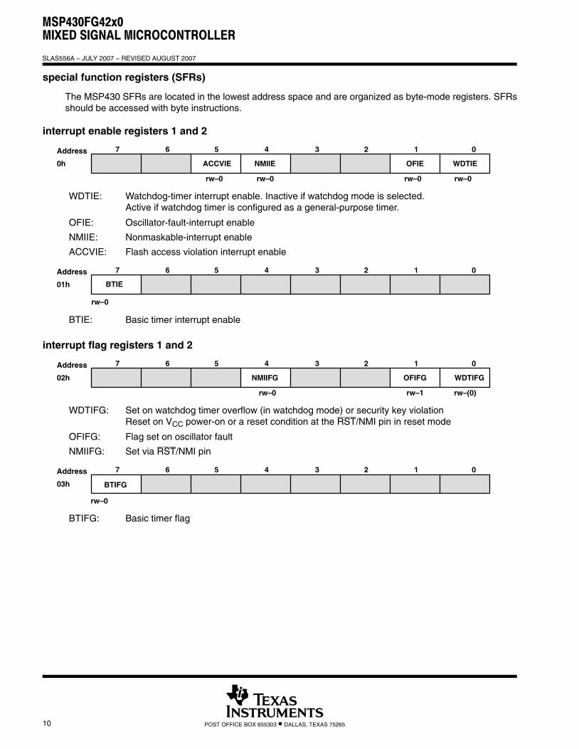
special function registers (SFRs)
The MSP430 SFRs are located in the lowest address space and are organized as byte-mode registers. SFRsshould be accessed with byte instructions.
interrupt enable registers 1 and 2
7 6 5 4 0
OFIE WDTIE
3 2 1
rw–0 rw–0 rw–0
Address
0h ACCVIE NMIIE
rw–0
WDTIE: Watchdog-timer interrupt enable. Inactive if watchdog mode is selected.Active if watchdog timer is configured as a general-purpose timer.
OFIE: Oscillator-fault-interrupt enable
NMIIE: Nonmaskable-interrupt enable
ACCVIE: Flash access violation interrupt enable
7 6 5 4 03 2 1Address
01h
rw–0
BTIE
BTIE: Basic timer interrupt enable
interrupt flag registers 1 and 2
7 6 5 4 0
OFIFG WDTIFG
3 2 1
rw–0 rw–1 rw–(0)
Address
02h NMIIFG
WDTIFG: Set on watchdog timer overflow (in watchdog mode) or security key violationReset on VCC power-on or a reset condition at the RST/NMI pin in reset mode
OFIFG: Flag set on oscillator fault
NMIIFG: Set via RST/NMI pin
7 6 5 4 03 2 1Address
03h BTIFG
rw–0
BTIFG: Basic timer flag
MSP430FG42x0MIXED SIGNAL MICROCONTROLLER
SLAS556A − JULY 2007 − REVISED AUGUST 2007
11POST OFFICE BOX 655303 • DALLAS, TEXAS 75265
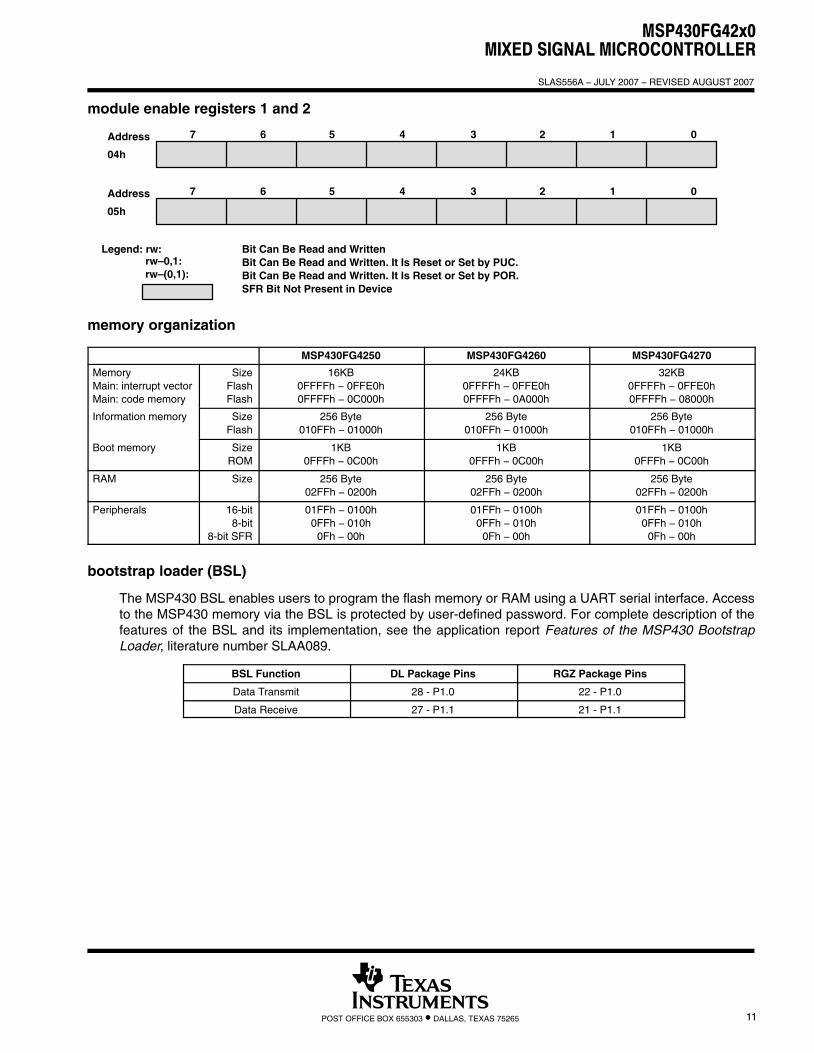
module enable registers 1 and 2
7 6 5 4 03 2 1Address
04h
7 6 5 4 03 2 1Address
05h
rw–0,1:Legend: rw: Bit Can Be Read and Written
Bit Can Be Read and Written. It Is Reset or Set by PUC.Bit Can Be Read and Written. It Is Reset or Set by POR.SFR Bit Not Present in Device
rw–(0,1):
memory organization
MSP430FG4250 MSP430FG4260 MSP430FG4270
MemoryMain: interrupt vectorMain: code memory
SizeFlashFlash
16KB0FFFFh − 0FFE0h0FFFFh − 0C000h
24KB0FFFFh − 0FFE0h0FFFFh − 0A000h
32KB0FFFFh − 0FFE0h0FFFFh − 08000h
Information memory SizeFlash
256 Byte010FFh − 01000h
256 Byte010FFh − 01000h
256 Byte010FFh − 01000h
Boot memory SizeROM
1KB0FFFh − 0C00h
1KB0FFFh − 0C00h
1KB0FFFh − 0C00h
RAM Size 256 Byte02FFh − 0200h
256 Byte02FFh − 0200h
256 Byte02FFh − 0200h
Peripherals 16-bit8-bit
8-bit SFR
01FFh − 0100h0FFh − 010h
0Fh − 00h
01FFh − 0100h0FFh − 010h
0Fh − 00h
01FFh − 0100h0FFh − 010h
0Fh − 00h
bootstrap loader (BSL)
The MSP430 BSL enables users to program the flash memory or RAM using a UART serial interface. Accessto the MSP430 memory via the BSL is protected by user-defined password. For complete description of thefeatures of the BSL and its implementation, see the application report Features of the MSP430 BootstrapLoader, literature number SLAA089.
BSL Function DL Package Pins RGZ Package Pins
Data Transmit 28 - P1.0 22 - P1.0
Data Receive 27 - P1.1 21 - P1.1
MSP430FG42x0MIXED SIGNAL MICROCONTROLLER
SLAS556A − JULY 2007 − REVISED AUGUST 2007
12 POST OFFICE BOX 655303 • DALLAS, TEXAS 75265
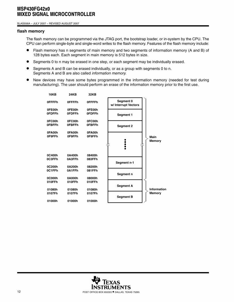
flash memory
The flash memory can be programmed via the JTAG port, the bootstrap loader, or in-system by the CPU. TheCPU can perform single-byte and single-word writes to the flash memory. Features of the flash memory include:
� Flash memory has n segments of main memory and two segments of information memory (A and B) of128 bytes each. Each segment in main memory is 512 bytes in size.
� Segments 0 to n may be erased in one step, or each segment may be individually erased.
� Segments A and B can be erased individually, or as a group with segments 0 to n.Segments A and B are also called information memory.
� New devices may have some bytes programmed in the information memory (needed for test duringmanufacturing). The user should perform an erase of the information memory prior to the first use.
Segment 0w/ Interrupt Vectors
Segment 1
Segment 2
Segment n-1
Segment n
Segment A
Segment B
MainMemory
InformationMemory
32KB
0FFFFh
0FE00h0FDFFh
0FC00h0FBFFh
0FA00h0F9FFh
08400h083FFh
08200h081FFh
08000h010FFh
01080h0107Fh
01000h
24KB
0FFFFh
0FE00h0FDFFh
0FC00h0FBFFh
0FA00h0F9FFh
0A400h0A3FFh
0A200h0A1FFh
0A000h010FFh
01080h0107Fh
01000h
16KB
0FFFFh
0FE00h0FDFFh
0FC00h0FBFFh
0FA00h0F9FFh
0C400h0C3FFh
0C200h0C1FFh
0C000h010FFh
01080h0107Fh
01000h
MSP430FG42x0MIXED SIGNAL MICROCONTROLLER
SLAS556A − JULY 2007 − REVISED AUGUST 2007
13POST OFFICE BOX 655303 • DALLAS, TEXAS 75265
peripherals
Peripherals are connected to the CPU through data, address, and control buses and can be handled using allinstructions. For complete module descriptions, refer to the MSP430x4xx Family User’s Guide, literaturenumber SLAU056.
oscillator and system clock
The clock system in the MSP430FG42x0 family of devices is supported by the FLL+ module, which includessupport for a 32768-Hz watch crystal oscillator, an internal digitally-controlled oscillator (DCO) and ahigh-frequency crystal oscillator. The FLL+ clock module is designed to meet the requirements of both lowsystem cost and low-power consumption. The FLL+ features digital frequency locked loop (FLL) hardware that,in conjunction with a digital modulator, stabilizes the DCO frequency to a programmable multiple of the watchcrystal frequency. The internal DCO provides a fast turn-on clock source and stabilizes in less than 6 μs. TheFLL+ module provides the following clock signals:
� Auxiliary clock (ACLK), sourced from a 32768-Hz watch crystal or a high-frequency crystal
� Main clock (MCLK), the system clock used by the CPU
� Sub-Main clock (SMCLK), the sub-system clock used by the peripheral modules
� ACLK/n, the buffered output of ACLK, ACLK/2, ACLK/4, or ACLK/8
brownout
The brownout circuit is implemented to provide the proper internal reset signal to the device during power-onand power-off. The CPU begins code execution after the brownout circuit releases the device reset. However,VCC may not have ramped to VCC(min) at that time. The user must ensure the default FLL+ settings are notchanged until VCC reaches VCC(min).
digital I/O
There are four 8-bit I/O ports implemented—ports P1, P2, P5, and P6:
� All individual I/O bits are independently programmable.� Any combination of input, output, and interrupt conditions is possible.� Edge-selectable interrupt input capability for all the eight bits of ports P1 and P2.� Read/write access to port-control registers is supported by all instructions.
Basic Timer1
Basic Timer1 has two independent 8-bit timers that can be cascaded to form a 16-bit timer/counter. Both timerscan be read and written by software. Basic Timer1 can be used to generate periodic interrupts.
LCD driver with regulated charge pump
The LCD_A driver generates the segment and common signals required to drive an LCD display. The LCD_Acontroller has dedicated data memory to hold segment drive information. Common and segment signals aregenerated as defined by the mode. Static, 2−MUX, 3−MUX, and 4−MUX LCDs are supported by this peripheral.The module can provide a LCD voltage independent of the supply voltage via an integrated charge pump.Furthermore, it is possible to control the level of the LCD voltage and thus contrast in software.
watchdog timer
The primary function of the watchdog timer (WDT+) module is to perform a controlled system restart after asoftware problem occurs. If the selected time interval expires, a system reset is generated. If the watchdogfunction is not needed in an application, the module can be configured as an interval timer and can generateinterrupts at selected time intervals.
MSP430FG42x0MIXED SIGNAL MICROCONTROLLER
SLAS556A − JULY 2007 − REVISED AUGUST 2007
14 POST OFFICE BOX 655303 • DALLAS, TEXAS 75265
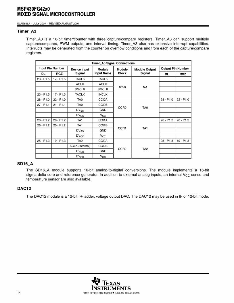
Timer_A3
Timer_A3 is a 16-bit timer/counter with three capture/compare registers. Timer_A3 can support multiplecapture/compares, PWM outputs, and interval timing. Timer_A3 also has extensive interrupt capabilities.Interrupts may be generated from the counter on overflow conditions and from each of the capture/compareregisters.
Timer_A3 Signal Connections
Input Pin Number Device Input Module Module Module Output Output Pin Number
DL RGZDevice Input
SignalModule
Input NameModuleBlock
Module OutputSignal DL RGZDL RGZ Signal Input Name Block Signal DL RGZ
23 - P1.5 17 - P1.5 TACLK TACLK
ACLK ACLKTimer NA
SMCLK SMCLKTimer NA
23 - P1.5 17 - P1.5 TACLK INCLK
28 - P1.0 22 - P1.0 TA0 CCI0A 28 - P1.0 22 - P1.0
27 - P1.1 21 - P1.1 TA0 CCI0BCCR0 TA0
DVSS GNDCCR0 TA0
DVCC VCC
26 - P1.2 20 - P1.2 TA1 CCI1A 26 - P1.2 20 - P1.2
26 - P1.2 20 - P1.2 TA1 CCI1BCCR1 TA1
DVSS GNDCCR1 TA1
DVCC VCC
25 - P1.3 19 - P1.3 TA2 CCI2A 25 - P1.3 19 - P1.3
ACLK (internal) CCI2BCCR2 TA2
DVSS GNDCCR2 TA2
DVCC VCC
SD16_AThe SD16_A module supports 16-bit analog-to-digital conversions. The module implements a 16-bitsigma-delta core and reference generator. In addition to external analog inputs, an internal VCC sense andtemperature sensor are also available.
DAC12
The DAC12 module is a 12-bit, R-ladder, voltage output DAC. The DAC12 may be used in 8- or 12-bit mode.
MSP430FG42x0MIXED SIGNAL MICROCONTROLLER
SLAS556A − JULY 2007 − REVISED AUGUST 2007
15POST OFFICE BOX 655303 • DALLAS, TEXAS 75265
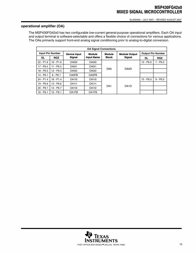
operational amplifier (OA)
The MSP430FG42x0 has two configurable low-current general-purpose operational amplifiers. Each OA inputand output terminal is software-selectable and offers a flexible choice of connections for various applications.The OAs primarily support front-end analog signal conditioning prior to analog-to-digital conversion.
OA Signal Connections
Input Pin Number Device Input Module Module Module Output Output Pin Number
DL RGZDevice Input
SignalModule
Input NameModuleBlock
Module OutputSignal DL RGZDL RGZ Signal Input Name Block Signal DL RGZ
22 - P1.6 16 - P1.6 OA0I0 OA0I0 13 - P6.0 7 - P6.0
17 - P6.4 11 - P6.4 OA0I1 OA0I1OA0 OA0O
18 - P6.5 12 - P6.5 OA0I2 OA0I2OA0 OA0O
14 - P6.1 8 - P6.1 OA0FB OA0FB
24 - P1.4 18 - P1.4 OA1I0 OA1I0 15 - P6.0 9 - P6.0
19 - P6.6 13 - P6.6 OA1I1 OA1I1OA1 OA1O
20 - P6.7 14 - P6.7 OA1I2 OA1I2OA1 OA1O
16 - P6.1 10 - P6.1 OA1FB OA1FB
MSP430FG42x0MIXED SIGNAL MICROCONTROLLER
SLAS556A − JULY 2007 − REVISED AUGUST 2007
16 POST OFFICE BOX 655303 • DALLAS, TEXAS 75265
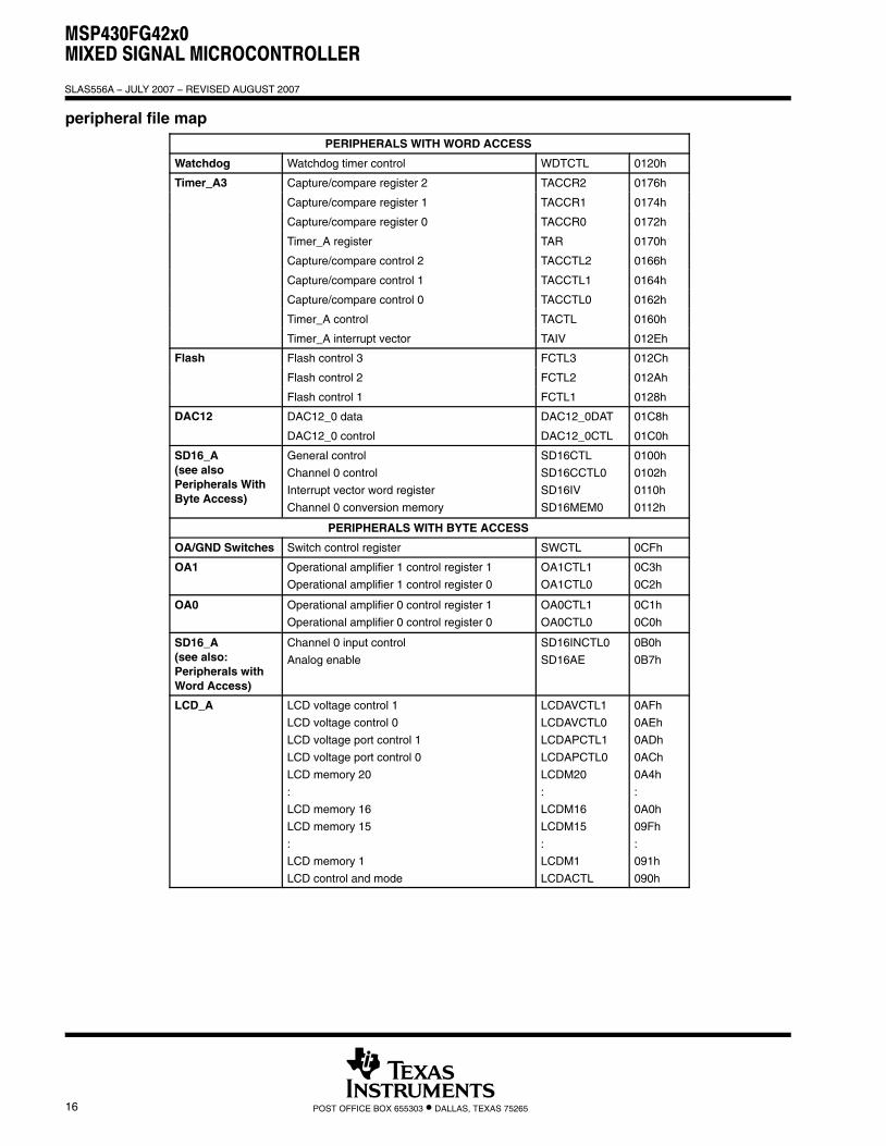
peripheral file map
PERIPHERALS WITH WORD ACCESS
Watchdog Watchdog timer control WDTCTL 0120h
Timer_A3 Capture/compare register 2 TACCR2 0176h_
Capture/compare register 1 TACCR1 0174h
Capture/compare register 0 TACCR0 0172h
Timer_A register TAR 0170h
Capture/compare control 2 TACCTL2 0166h
Capture/compare control 1 TACCTL1 0164h
Capture/compare control 0 TACCTL0 0162h
Timer_A control TACTL 0160h
Timer_A interrupt vector TAIV 012Eh
Flash Flash control 3 FCTL3 012Ch
Flash control 2 FCTL2 012Ah
Flash control 1 FCTL1 0128h
DAC12 DAC12_0 data DAC12_0DAT 01C8h
DAC12_0 control DAC12_0CTL 01C0h
SD16_A(see alsoPeripherals WithByte Access)
General control
Channel 0 control
Interrupt vector word register
Channel 0 conversion memory
SD16CTL
SD16CCTL0
SD16IV
SD16MEM0
0100h
0102h
0110h
0112h
PERIPHERALS WITH BYTE ACCESS
OA/GND Switches Switch control register SWCTL 0CFh
OA1 Operational amplifier 1 control register 1
Operational amplifier 1 control register 0
OA1CTL1
OA1CTL0
0C3h
0C2h
OA0 Operational amplifier 0 control register 1
Operational amplifier 0 control register 0
OA0CTL1
OA0CTL0
0C1h
0C0h
SD16_A(see also:Peripherals withWord Access)
Channel 0 input control
Analog enable
SD16INCTL0
SD16AE
0B0h
0B7h
LCD_A LCD voltage control 1
LCD voltage control 0
LCD voltage port control 1
LCD voltage port control 0
LCD memory 20
:
LCD memory 16
LCD memory 15
:
LCD memory 1
LCD control and mode
LCDAVCTL1
LCDAVCTL0
LCDAPCTL1
LCDAPCTL0
LCDM20
:
LCDM16
LCDM15
:
LCDM1
LCDACTL
0AFh
0AEh
0ADh
0ACh
0A4h
:
0A0h
09Fh
:
091h
090h
MSP430FG42x0MIXED SIGNAL MICROCONTROLLER
SLAS556A − JULY 2007 − REVISED AUGUST 2007
17POST OFFICE BOX 655303 • DALLAS, TEXAS 75265
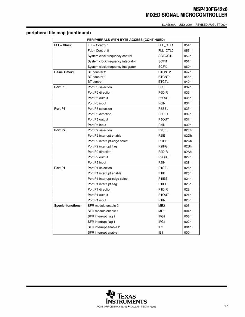
peripheral file map (continued)
PERIPHERALS WITH BYTE ACCESS (CONTINUED)
FLL+ Clock FLL+ Control 1 FLL_CTL1 054h
FLL+ Control 0 FLL_CTL0 053h
System clock frequency control SCFQCTL 052h
System clock frequency integrator SCFI1 051h
System clock frequency integrator SCFI0 050h
Basic Timer1 BT counter 2
BT counter 1
BT control
BTCNT2
BTCNT1
BTCTL
047h
046h
040h
Port P6 Port P6 selection P6SEL 037h
Port P6 direction P6DIR 036h
Port P6 output P6OUT 035h
Port P6 input P6IN 034h
Port P5 Port P5 selection P5SEL 033h
Port P5 direction P5DIR 032h
Port P5 output P5OUT 031h
Port P5 input P5IN 030h
Port P2 Port P2 selection P2SEL 02Eh
Port P2 interrupt enable P2IE 02Dh
Port P2 interrupt-edge select P2IES 02Ch
Port P2 interrupt flag P2IFG 02Bh
Port P2 direction P2DIR 02Ah
Port P2 output P2OUT 029h
Port P2 input P2IN 028h
Port P1 Port P1 selection P1SEL 026h
Port P1 interrupt enable P1IE 025h
Port P1 interrupt-edge select P1IES 024h
Port P1 interrupt flag P1IFG 023h
Port P1 direction P1DIR 022h
Port P1 output P1OUT 021h
Port P1 input P1IN 020h
Special functions SFR module enable 2 ME2 005hp
SFR module enable 1 ME1 004h
SFR interrupt flag 2 IFG2 003h
SFR interrupt flag 1 IFG1 002h
SFR interrupt enable 2 IE2 001h
SFR interrupt enable 1 IE1 000h
MSP430FG42x0MIXED SIGNAL MICROCONTROLLER
SLAS556A − JULY 2007 − REVISED AUGUST 2007
18 POST OFFICE BOX 655303 • DALLAS, TEXAS 75265
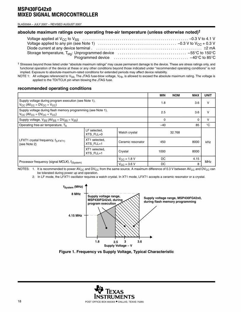
absolute maximum ratings over operating free-air temperature (unless otherwise noted)†
Voltage applied at VCC to VSS −0.3 V to 4.1 V. . . . . . . . . . . . . . . . . . . . . . . . . . . . . . . . . . . . . . . . . . . . . . . . . . . . . . Voltage applied to any pin (see Note 1) −0.3 V to VCC + 0.3 V. . . . . . . . . . . . . . . . . . . . . . . . . . . . . . . . . . . . . . . . Diode current at any device terminal . ±2 mA. . . . . . . . . . . . . . . . . . . . . . . . . . . . . . . . . . . . . . . . . . . . . . . . . . . . . . Storage temperature, Tstg: Unprogrammed device −55°C to 150°C. . . . . . . . . . . . . . . . . . . . . . . . . . . . . . . . . . .
Programmed device −40°C to 85°C. . . . . . . . . . . . . . . . . . . . . . . . . . . . . . . . . . . . . . † Stresses beyond those listed under “absolute maximum ratings” may cause permanent damage to the device. These are stress ratings only, and
functional operation of the device at these or any other conditions beyond those indicated under “recommended operating conditions” is notimplied. Exposure to absolute-maximum-rated conditions for extended periods may affect device reliability.
NOTE 1: All voltages referenced to VSS. The JTAG fuse-blow voltage, VFB, is allowed to exceed the absolute maximum rating. The voltage isapplied to the TDI/TCLK pin when blowing the JTAG fuse.
recommended operating conditions
MIN NOM MAX UNIT
Supply voltage during program execution (see Note 1), VCC (AVCC = DVCC = VCC)
1.8 3.6 V
Supply voltage during flash memory programming (see Note 1),VCC (AVCC = DVCC = VCC)
2.5 3.6 V
Supply voltage, VSS (AVSS = DVSS = VSS) 0 0 V
Operating free-air temperature, TA −40 85 °C
LF selected,XTS_FLL=0
Watch crystal 32.768
LFXT1 crystal frequency, f(LFXT1)(see Note 2)
XT1 selected,XTS_FLL=1
Ceramic resonator 450 8000 kHz(see Note 2)
XT1 selected,XTS_FLL=1
Crystal 1000 8000
Processor frequency (signal MCLK) fVCC = 1.8 V DC 4.15
MHzProcessor frequency (signal MCLK), f(System) VCC = 3.6 V DC 8MHz
NOTES: 1. It is recommended to power AVCC and DVCC from the same source. A maximum difference of 0.3 V between AVCC and DVCC canbe tolerated during power up and operation.
2. In LF mode, the LFXT1 oscillator requires a watch crystal. In XT1 mode, LFXT1 accepts a ceramic resonator or a crystal.
1.8 3.63
ÎÎÎÎÎÎÎÎÎÎÎÎÎÎÎÎÎÎÎÎÎÎÎÎÎÎÎÎÎÎÎÎÎÎÎÎÎÎÎÎÎÎÎÎÎ
4.15 MHz
8 MHz
Supply Voltage − V
Supply voltage range, MSP430FG42x0,during flash memory programming
Supply voltage range,MSP430FG42x0, duringprogram execution
2.5
fSystem (MHz)
Figure 1. Frequency vs Supply Voltage, Typical Characteristic
MSP430FG42x0MIXED SIGNAL MICROCONTROLLER
SLAS556A − JULY 2007 − REVISED AUGUST 2007
19POST OFFICE BOX 655303 • DALLAS, TEXAS 75265
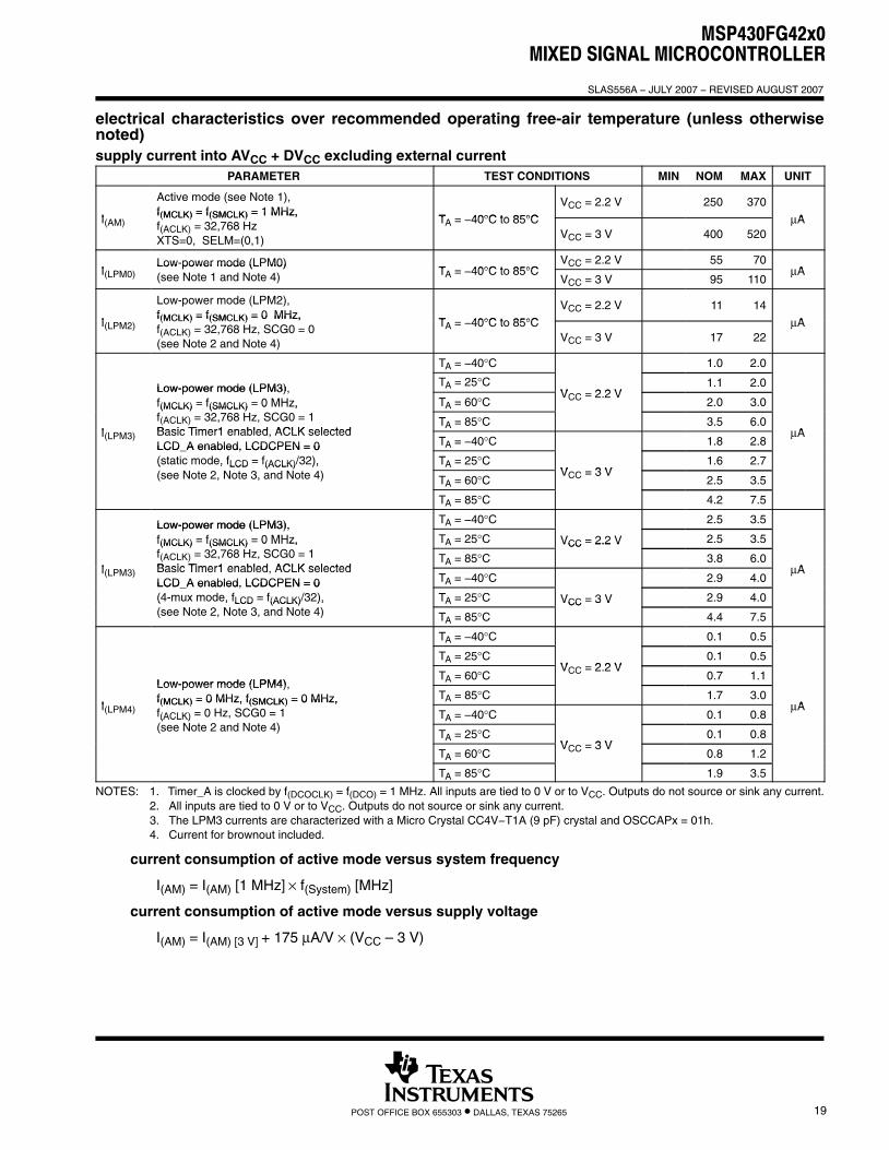
electrical characteristics over recommended operating free-air temperature (unless otherwisenoted)supply current into AVCC + DVCC excluding external current
PARAMETER TEST CONDITIONS MIN NOM MAX UNIT
I
Active mode (see Note 1), f(MCLK) = f(SMCLK) = 1 MHz,
T 40°C to 85°CVCC = 2.2 V 250 370
AI(AM)f(MCLK) = f(SMCLK) = 1 MHz,f(ACLK) = 32,768 HzXTS=0, SELM=(0,1)
TA = −40°C to 85°CVCC = 3 V 400 520
μA
ILow-power mode (LPM0)
T 40°C to 85°CVCC = 2.2 V 55 70
AI(LPM0)Low power mode (LPM0) (see Note 1 and Note 4) TA = −40°C to 85°C
VCC = 3 V 95 110μA
I
Low-power mode (LPM2), f(MCLK) = f(SMCLK) = 0 MHz,
T 40°C to 85°CVCC = 2.2 V 11 14
AI(LPM2)f(MCLK) = f(SMCLK) = 0 MHz,f(ACLK) = 32,768 Hz, SCG0 = 0 (see Note 2 and Note 4)
TA = −40°C to 85°CVCC = 3 V 17 22
μA
TA = −40°C 1.0 2.0
Low-power mode (LPM3), TA = 25°CV 2 2 V
1.1 2.0Low-power mode (LPM3), f(MCLK) = f(SMCLK) = 0 MHz, TA = 60°C
VCC = 2.2 V2.0 3.0
I
f(MCLK) f(SMCLK) 0 MHz,f(ACLK) = 32,768 Hz, SCG0 = 1Basic Timer1 enabled ACLK selected
TA = 85°C 3.5 6.0AI(LPM3) Basic Timer1 enabled, ACLK selected
LCD A enabled, LCDCPEN = 0 TA = −40°C 1.8 2.8μA
LCD_A enabled, LCDCPEN = 0 (static mode, fLCD = f(ACLK)/32), TA = 25°C
V 3 V1.6 2.7( , LCD (ACLK) ),
(see Note 2, Note 3, and Note 4) TA = 60°CVCC = 3 V
2.5 3.5
TA = 85°C 4.2 7.5
Low-power mode (LPM3), TA = −40°C 2.5 3.5Low-power mode (LPM3), f(MCLK) = f(SMCLK) = 0 MHz, TA = 25°C VCC = 2.2 V 2.5 3.5
I
f(MCLK) f(SMCLK) 0 MHz,f(ACLK) = 32,768 Hz, SCG0 = 1Basic Timer1 enabled ACLK selected
TA = 85°CVCC 2.2 V
3.8 6.0AI(LPM3) Basic Timer1 enabled, ACLK selected
LCD A enabled, LCDCPEN = 0 TA = −40°C 2.9 4.0μA
LCD_A enabled, LCDCPEN = 0 (4-mux mode, fLCD = f(ACLK)/32), TA = 25°C VCC = 3 V 2.9 4.0( , LCD (ACLK) ),(see Note 2, Note 3, and Note 4) TA = 85°C
VCC 3 V
4.4 7.5
TA = −40°C 0.1 0.5
TA = 25°CV 2 2 V
0.1 0.5
Low-power mode (LPM4)TA = 60°C
VCC = 2.2 V0.7 1.1
I
Low-power mode (LPM4), f(MCLK) = 0 MHz, f(SMCLK) = 0 MHz, TA = 85°C 1.7 3.0
AI(LPM4)f(MCLK) = 0 MHz, f(SMCLK) = 0 MHz,f(ACLK) = 0 Hz, SCG0 = 1 ( N t 2 d N t 4)
TA = −40°C 0.1 0.8μA
(ACLK)(see Note 2 and Note 4)
TA = 25°CV 3 V
0.1 0.8
TA = 60°CVCC = 3 V
0.8 1.2
TA = 85°C 1.9 3.5
NOTES: 1. Timer_A is clocked by f(DCOCLK) = f(DCO) = 1 MHz. All inputs are tied to 0 V or to VCC. Outputs do not source or sink any current.2. All inputs are tied to 0 V or to VCC. Outputs do not source or sink any current.3. The LPM3 currents are characterized with a Micro Crystal CC4V−T1A (9 pF) crystal and OSCCAPx = 01h.4. Current for brownout included.
current consumption of active mode versus system frequency
I(AM) = I(AM) [1 MHz] × f(System) [MHz]
current consumption of active mode versus supply voltage
I(AM) = I(AM) [3 V] + 175 μA/V × (VCC – 3 V)
MSP430FG42x0MIXED SIGNAL MICROCONTROLLER
SLAS556A − JULY 2007 − REVISED AUGUST 2007
20 POST OFFICE BOX 655303 • DALLAS, TEXAS 75265
electrical characteristics over recommended operating free-air temperature (unless otherwisenoted) (continued)
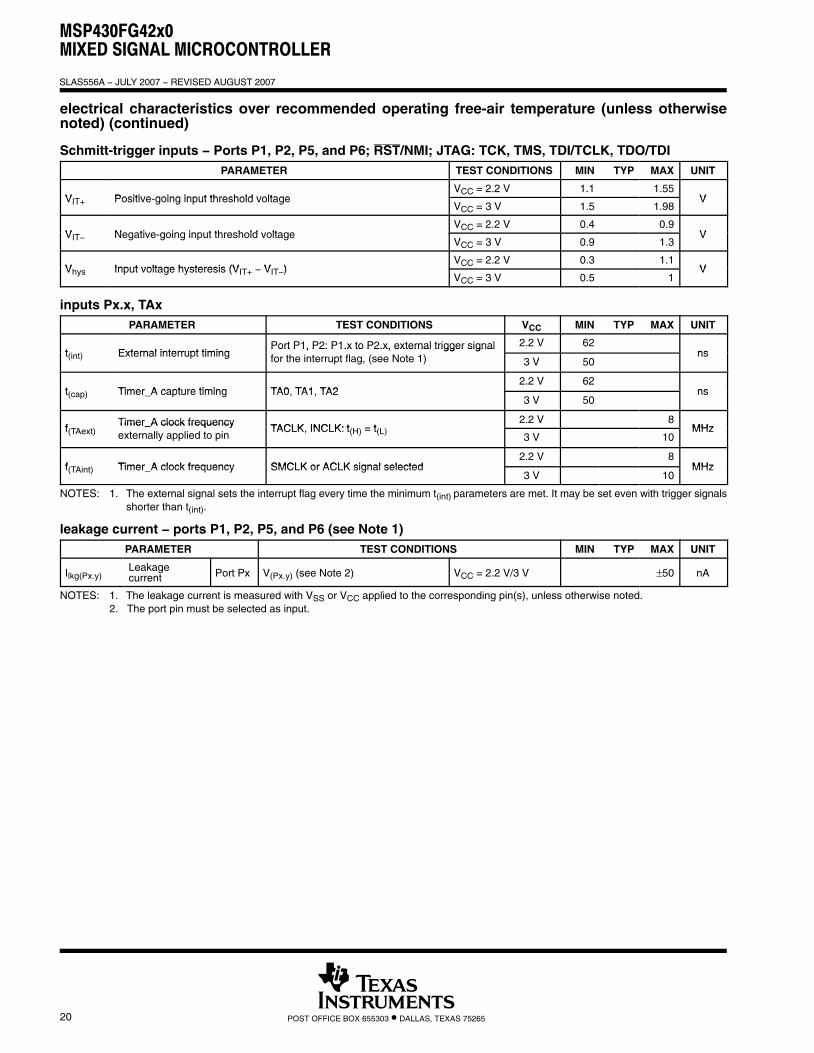
Schmitt-trigger inputs − Ports P1, P2, P5, and P6; RST/NMI; JTAG: TCK, TMS, TDI/TCLK, TDO/TDIPARAMETER TEST CONDITIONS MIN TYP MAX UNIT
V Positive going input threshold voltageVCC = 2.2 V 1.1 1.55
VVIT+ Positive-going input threshold voltageVCC = 3 V 1.5 1.98
V
V Negative going input threshold voltageVCC = 2.2 V 0.4 0.9
VVIT− Negative-going input threshold voltageVCC = 3 V 0.9 1.3
V
V Input voltage hysteresis (V V )VCC = 2.2 V 0.3 1.1
VVhys Input voltage hysteresis (VIT+ − VIT−)VCC = 3 V 0.5 1
V
inputs Px.x, TAxPARAMETER TEST CONDITIONS VCC MIN TYP MAX UNIT
t External interrupt timingPort P1, P2: P1.x to P2.x, external trigger signal 2.2 V 62
nst(int) External interrupt timingPort P1, P2: P1.x to P2.x, external trigger signalfor the interrupt flag, (see Note 1) 3 V 50
ns
t Timer A capture timing TA0 TA1 TA22.2 V 62
nst(cap) Timer_A capture timing TA0, TA1, TA23 V 50
ns
fTimer_A clock frequency
TACLK INCLK: t = t2.2 V 8
MHzf(TAext)Timer_A clock frequencyexternally applied to pin
TACLK, INCLK: t(H) = t(L)3 V 10
MHz
f Timer A clock frequency SMCLK or ACLK signal selected2.2 V 8
MHzf(TAint) Timer_A clock frequency SMCLK or ACLK signal selected3 V 10
MHz
NOTES: 1. The external signal sets the interrupt flag every time the minimum t(int) parameters are met. It may be set even with trigger signalsshorter than t(int).
leakage current − ports P1, P2, P5, and P6 (see Note 1)PARAMETER TEST CONDITIONS MIN TYP MAX UNIT
Ilkg(Px.y)Leakagecurrent Port Px V(Px.y) (see Note 2) VCC = 2.2 V/3 V ±50 nA
NOTES: 1. The leakage current is measured with VSS or VCC applied to the corresponding pin(s), unless otherwise noted.2. The port pin must be selected as input.
MSP430FG42x0MIXED SIGNAL MICROCONTROLLER
SLAS556A − JULY 2007 − REVISED AUGUST 2007
21POST OFFICE BOX 655303 • DALLAS, TEXAS 75265
electrical characteristics over recommended operating free-air temperature (unless otherwisenoted) (continued)
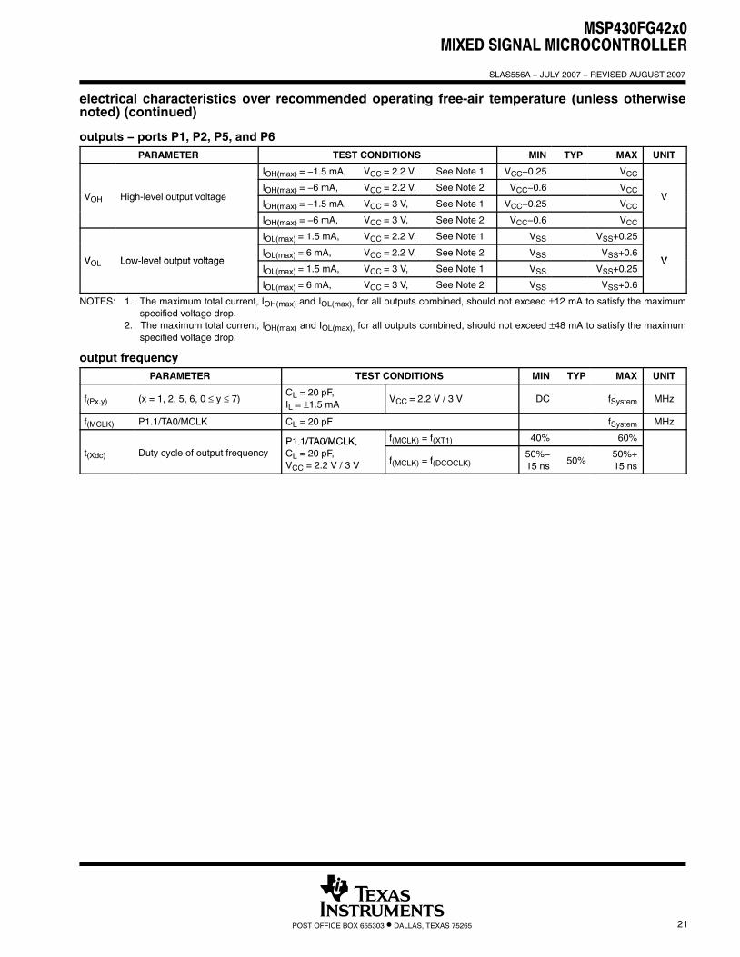
outputs − ports P1, P2, P5, and P6PARAMETER TEST CONDITIONS MIN TYP MAX UNIT
IOH(max) = −1.5 mA, VCC = 2.2 V, See Note 1 VCC−0.25 VCC
V High level output voltageIOH(max) = −6 mA, VCC = 2.2 V, See Note 2 VCC−0.6 VCC
VVOH High-level output voltageIOH(max) = −1.5 mA, VCC = 3 V, See Note 1 VCC−0.25 VCC
V
IOH(max) = −6 mA, VCC = 3 V, See Note 2 VCC−0.6 VCC
IOL(max) = 1.5 mA, VCC = 2.2 V, See Note 1 VSS VSS+0.25
V Low level output voltageIOL(max) = 6 mA, VCC = 2.2 V, See Note 2 VSS VSS+0.6
VVOL Low-level output voltageIOL(max) = 1.5 mA, VCC = 3 V, See Note 1 VSS VSS+0.25
V
IOL(max) = 6 mA, VCC = 3 V, See Note 2 VSS VSS+0.6
NOTES: 1. The maximum total current, IOH(max) and IOL(max), for all outputs combined, should not exceed ±12 mA to satisfy the maximumspecified voltage drop.
2. The maximum total current, IOH(max) and IOL(max), for all outputs combined, should not exceed ±48 mA to satisfy the maximumspecified voltage drop.
output frequencyPARAMETER TEST CONDITIONS MIN TYP MAX UNIT
f(Px.y) (x = 1, 2, 5, 6, 0 ≤ y ≤ 7)CL = 20 pF,IL = ±1.5 mA
VCC = 2.2 V / 3 V DC fSystem MHz
f(MCLK) P1.1/TA0/MCLK CL = 20 pF fSystem MHz
P1.1/TA0/MCLK, f(MCLK) = f(XT1) 40% 60%
t(Xdc) Duty cycle of output frequencyP1.1/TA0/MCLK,CL = 20 pF,VCC = 2.2 V / 3 V f(MCLK) = f(DCOCLK)
50%−15 ns
50%50%+15 ns
MSP430FG42x0MIXED SIGNAL MICROCONTROLLER
SLAS556A − JULY 2007 − REVISED AUGUST 2007
22 POST OFFICE BOX 655303 • DALLAS, TEXAS 75265
electrical characteristics over recommended operating free-air temperature (unless otherwisenoted) (continued)
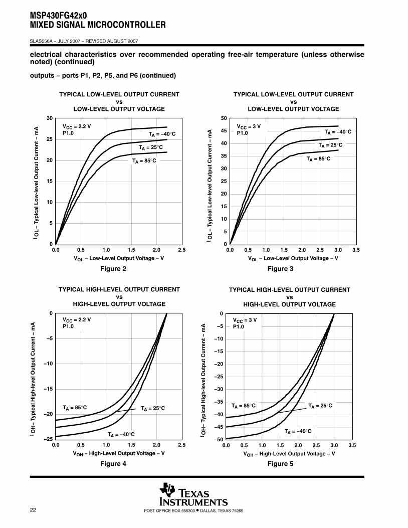
outputs − ports P1, P2, P5, and P6 (continued)
Figure 2
VOL − Low-Level Output Voltage − V
0
5
10
15
20
25
30
0.0 0.5 1.0 1.5 2.0 2.5
VCC = 2.2 VP1.0
TYPICAL LOW-LEVEL OUTPUT CURRENTvs
LOW-LEVEL OUTPUT VOLTAGE
TA = 25°C
TA = 85°C
OL
I−
Typ
ical
Lo
w-l
evel
Ou
tpu
t C
urr
ent
− m
A
TA = −40°C
Figure 3
VOL − Low-Level Output Voltage − V
0
5
10
15
20
25
30
35
40
45
50
0.0 0.5 1.0 1.5 2.0 2.5 3.0 3.5
VCC = 3 VP1.0
TYPICAL LOW-LEVEL OUTPUT CURRENTvs
LOW-LEVEL OUTPUT VOLTAGE
TA = 25°C
TA = 85°C
OL
I−
Typ
ical
Lo
w-l
evel
Ou
tpu
t C
urr
ent
− m
A TA = −40°C
Figure 4
VOH − High-Level Output Voltage − V
−25
−20
−15
−10
−5
0
0.0 0.5 1.0 1.5 2.0 2.5
VCC = 2.2 VP1.0
TYPICAL HIGH-LEVEL OUTPUT CURRENTvs
HIGH-LEVEL OUTPUT VOLTAGE
TA = 25°CTA = 85°C
OH
I−
Typ
ical
Hig
h-l
evel
Ou
tpu
t C
urr
ent
− m
A
TA = −40°C
Figure 5
VOH − High-Level Output Voltage − V
−50
−45
−40
−35
−30
−25
−20
−15
−10
−5
0
0.0 0.5 1.0 1.5 2.0 2.5 3.0 3.5
VCC = 3 VP1.0
TYPICAL HIGH-LEVEL OUTPUT CURRENTvs
HIGH-LEVEL OUTPUT VOLTAGE
TA = 25°CTA = 85°C
OH
I−
Typ
ical
Hig
h-l
evel
Ou
tpu
t C
urr
ent
− m
A
TA = −40°C
MSP430FG42x0MIXED SIGNAL MICROCONTROLLER
SLAS556A − JULY 2007 − REVISED AUGUST 2007
23POST OFFICE BOX 655303 • DALLAS, TEXAS 75265
electrical characteristics over recommended operating free-air temperature (unless otherwisenoted) (continued)
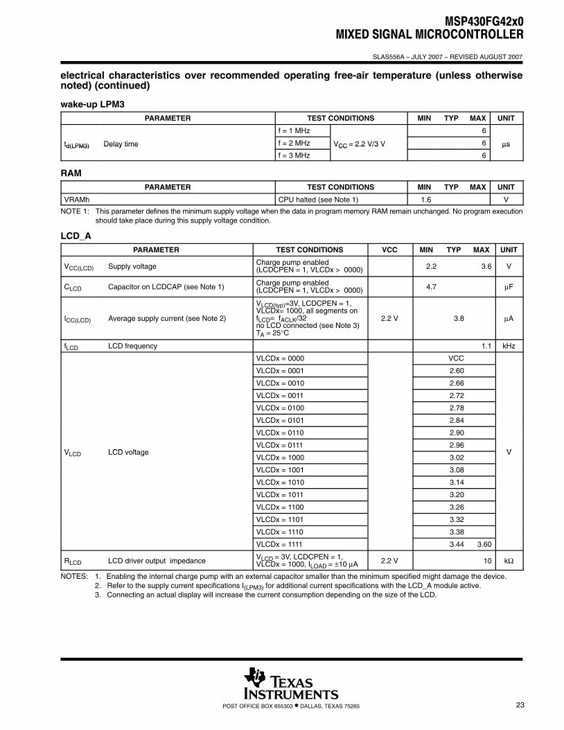
wake-up LPM3PARAMETER TEST CONDITIONS MIN TYP MAX UNIT
f = 1 MHz 6
td(LPM3) Delay time f = 2 MHz VCC = 2.2 V/3 V 6 μstd(LPM3) Delay time
f = 3 MHz
VCC 2.2 V/3 V
6
μs
RAMPARAMETER TEST CONDITIONS MIN TYP MAX UNIT
VRAMh CPU halted (see Note 1) 1.6 V
NOTE 1: This parameter defines the minimum supply voltage when the data in program memory RAM remain unchanged. No program executionshould take place during this supply voltage condition.
LCD_APARAMETER TEST CONDITIONS VCC MIN TYP MAX UNIT
VCC(LCD) Supply voltage Charge pump enabled(LCDCPEN = 1, VLCDx > 0000) 2.2 3.6 V
CLCD Capacitor on LCDCAP (see Note 1) Charge pump enabled(LCDCPEN = 1, VLCDx > 0000) 4.7 μF
ICC(LCD) Average supply current (see Note 2)
VLCD(typ)=3V, LCDCPEN = 1,VLCDx= 1000, all segments onfLCD= fACLK/32no LCD connected (see Note 3)TA = 25°C
2.2 V 3.8 μA
fLCD LCD frequency 1.1 kHz
VLCDx = 0000 VCC
VLCDx = 0001 2.60
VLCDx = 0010 2.66
VLCDx = 0011 2.72
VLCDx = 0100 2.78
VLCDx = 0101 2.84
VLCDx = 0110 2.90
V LCD voltageVLCDx = 0111 2.96
VVLCD LCD voltageVLCDx = 1000 3.02
V
VLCDx = 1001 3.08
VLCDx = 1010 3.14
VLCDx = 1011 3.20
VLCDx = 1100 3.26
VLCDx = 1101 3.32
VLCDx = 1110 3.38
VLCDx = 1111 3.44 3.60
RLCD LCD driver output impedance VLCD = 3V, LCDCPEN = 1,VLCDx = 1000, ILOAD = ±10 μA 2.2 V 10 kΩ
NOTES: 1. Enabling the internal charge pump with an external capacitor smaller than the minimum specified might damage the device.2. Refer to the supply current specifications I(LPM3) for additional current specifications with the LCD_A module active.3. Connecting an actual display will increase the current consumption depending on the size of the LCD.
MSP430FG42x0MIXED SIGNAL MICROCONTROLLER
SLAS556A − JULY 2007 − REVISED AUGUST 2007
24 POST OFFICE BOX 655303 • DALLAS, TEXAS 75265
electrical characteristics over recommended operating free-air temperature (unless otherwisenoted) (continued)
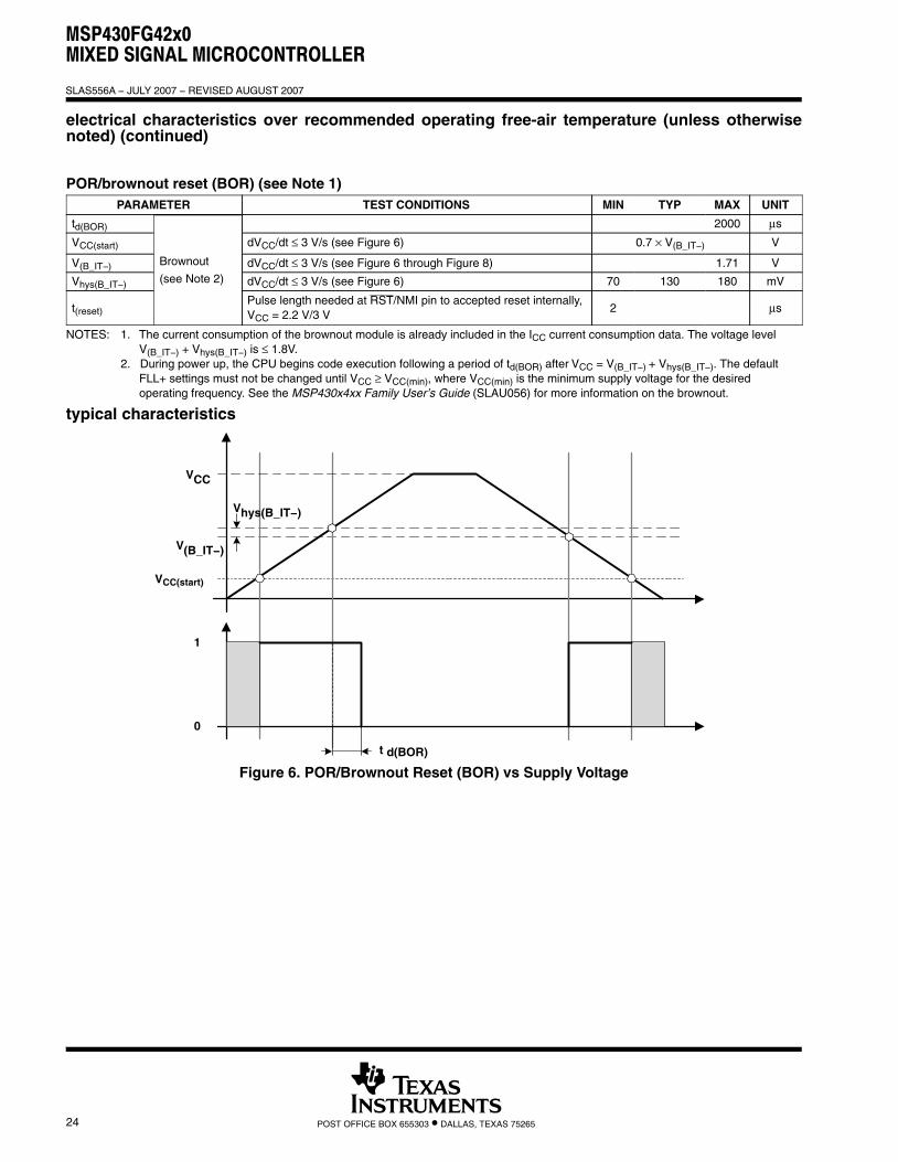
POR/brownout reset (BOR) (see Note 1)PARAMETER TEST CONDITIONS MIN TYP MAX UNIT
td(BOR) 2000 μs
VCC(start) dVCC/dt ≤ 3 V/s (see Figure 6) 0.7 × V(B_IT−) V
V(B_IT−) Brownout dVCC/dt ≤ 3 V/s (see Figure 6 through Figure 8) 1.71 V
Vhys(B_IT−) (see Note 2) dVCC/dt ≤ 3 V/s (see Figure 6) 70 130 180 mV
t(reset)Pulse length needed at RST/NMI pin to accepted reset internally,VCC = 2.2 V/3 V
2 μs
NOTES: 1. The current consumption of the brownout module is already included in the ICC current consumption data. The voltage level V(B_IT−) + Vhys(B_IT−) is ≤ 1.8V.
2. During power up, the CPU begins code execution following a period of td(BOR) after VCC = V(B_IT−) + Vhys(B_IT−). The defaultFLL+ settings must not be changed until VCC ≥ VCC(min), where VCC(min) is the minimum supply voltage for the desiredoperating frequency. See the MSP430x4xx Family User’s Guide (SLAU056) for more information on the brownout.
typical characteristics
0
1
t d(BOR)
VCC
V(B_IT−)
Vhys(B_IT−)
VCC(start)
Figure 6. POR/Brownout Reset (BOR) vs Supply Voltage
MSP430FG42x0MIXED SIGNAL MICROCONTROLLER
SLAS556A − JULY 2007 − REVISED AUGUST 2007
25POST OFFICE BOX 655303 • DALLAS, TEXAS 75265
electrical characteristics over recommended operating free-air temperature (unless otherwisenoted) (continued)
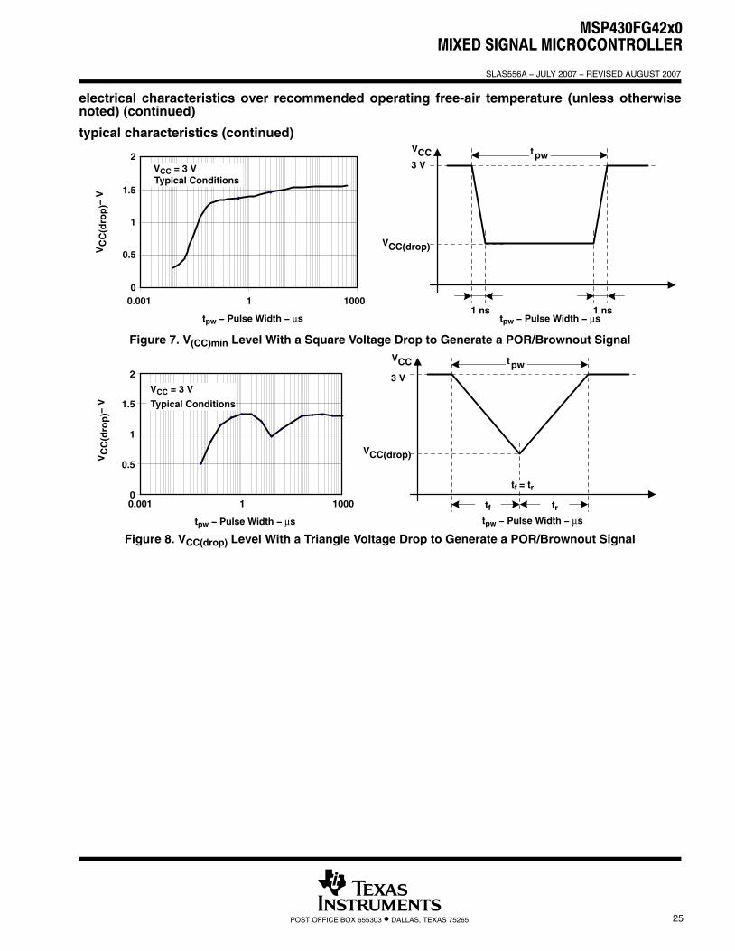
typical characteristics (continued)
VCC(drop)
VCC3 V
tpw
0
0.5
1
1.5
2
0.001 1 1000
Typical Conditions
1 ns 1 nstpw − Pulse Width − μs
VC
C(d
rop
)− V
tpw − Pulse Width − μs
VCC = 3 V
Figure 7. V(CC)min Level With a Square Voltage Drop to Generate a POR/Brownout SignalVCC
0
0.5
1
1.5
2
VCC(drop)
tpw
tpw − Pulse Width − μs
VC
C(d
rop
)− V
3 V
0.001 1 1000 tf trtpw − Pulse Width − μs
tf = tr
Typical Conditions
VCC = 3 V
Figure 8. VCC(drop) Level With a Triangle Voltage Drop to Generate a POR/Brownout Signal
MSP430FG42x0MIXED SIGNAL MICROCONTROLLER
SLAS556A − JULY 2007 − REVISED AUGUST 2007
26 POST OFFICE BOX 655303 • DALLAS, TEXAS 75265
electrical characteristics over recommended operating free-air temperature (unless otherwisenoted)
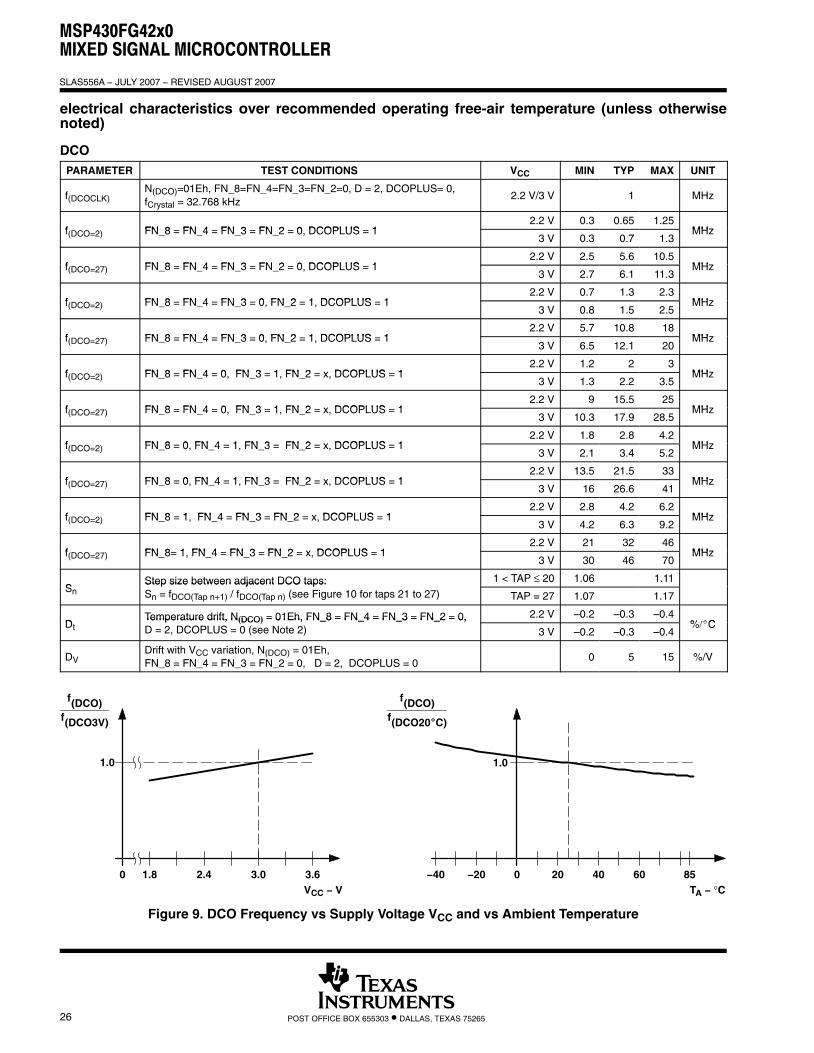
DCOPARAMETER TEST CONDITIONS VCC MIN TYP MAX UNIT
f(DCOCLK)N(DCO)=01Eh, FN_8=FN_4=FN_3=FN_2=0, D = 2, DCOPLUS= 0,fCrystal = 32.768 kHz
2.2 V/3 V 1 MHz
f FN 8 FN 4 FN 3 FN 2 0 DCOPLUS 12.2 V 0.3 0.65 1.25
MHzf(DCO=2) FN_8 = FN_4 = FN_3 = FN_2 = 0, DCOPLUS = 13 V 0.3 0.7 1.3
MHz
f FN 8 FN 4 FN 3 FN 2 0 DCOPLUS 12.2 V 2.5 5.6 10.5
MHzf(DCO=27) FN_8 = FN_4 = FN_3 = FN_2 = 0, DCOPLUS = 13 V 2.7 6.1 11.3
MHz
f FN 8 FN 4 FN 3 0 FN 2 1 DCOPLUS 12.2 V 0.7 1.3 2.3
MHzf(DCO=2) FN_8 = FN_4 = FN_3 = 0, FN_2 = 1, DCOPLUS = 13 V 0.8 1.5 2.5
MHz
f FN 8 FN 4 FN 3 0 FN 2 1 DCOPLUS 12.2 V 5.7 10.8 18
MHzf(DCO=27) FN_8 = FN_4 = FN_3 = 0, FN_2 = 1, DCOPLUS = 13 V 6.5 12.1 20
MHz
f FN 8 FN 4 0 FN 3 1 FN 2 x DCOPLUS 12.2 V 1.2 2 3
MHzf(DCO=2) FN_8 = FN_4 = 0, FN_3 = 1, FN_2 = x, DCOPLUS = 13 V 1.3 2.2 3.5
MHz
f FN 8 FN 4 0 FN 3 1 FN 2 x DCOPLUS 12.2 V 9 15.5 25
MHzf(DCO=27) FN_8 = FN_4 = 0, FN_3 = 1, FN_2 = x, DCOPLUS = 13 V 10.3 17.9 28.5
MHz
f FN 8 0 FN 4 1 FN 3 FN 2 x DCOPLUS 12.2 V 1.8 2.8 4.2
MHzf(DCO=2) FN_8 = 0, FN_4 = 1, FN_3 = FN_2 = x, DCOPLUS = 13 V 2.1 3.4 5.2
MHz
f FN 8 0 FN 4 1 FN 3 FN 2 x DCOPLUS 12.2 V 13.5 21.5 33
MHzf(DCO=27) FN_8 = 0, FN_4 = 1, FN_3 = FN_2 = x, DCOPLUS = 13 V 16 26.6 41
MHz
f FN 8 1 FN 4 FN 3 FN 2 x DCOPLUS 1 2.2 V 2.8 4.2 6.2
MHzf(DCO=2) FN_8 = 1, FN_4 = FN_3 = FN_2 = x, DCOPLUS = 13 V 4.2 6.3 9.2
MHz
f FN 8 1 FN 4 FN 3 FN 2 x DCOPLUS 1 2.2 V 21 32 46
MHzf(DCO=27) FN_8= 1, FN_4 = FN_3 = FN_2 = x, DCOPLUS = 13 V 30 46 70
MHz
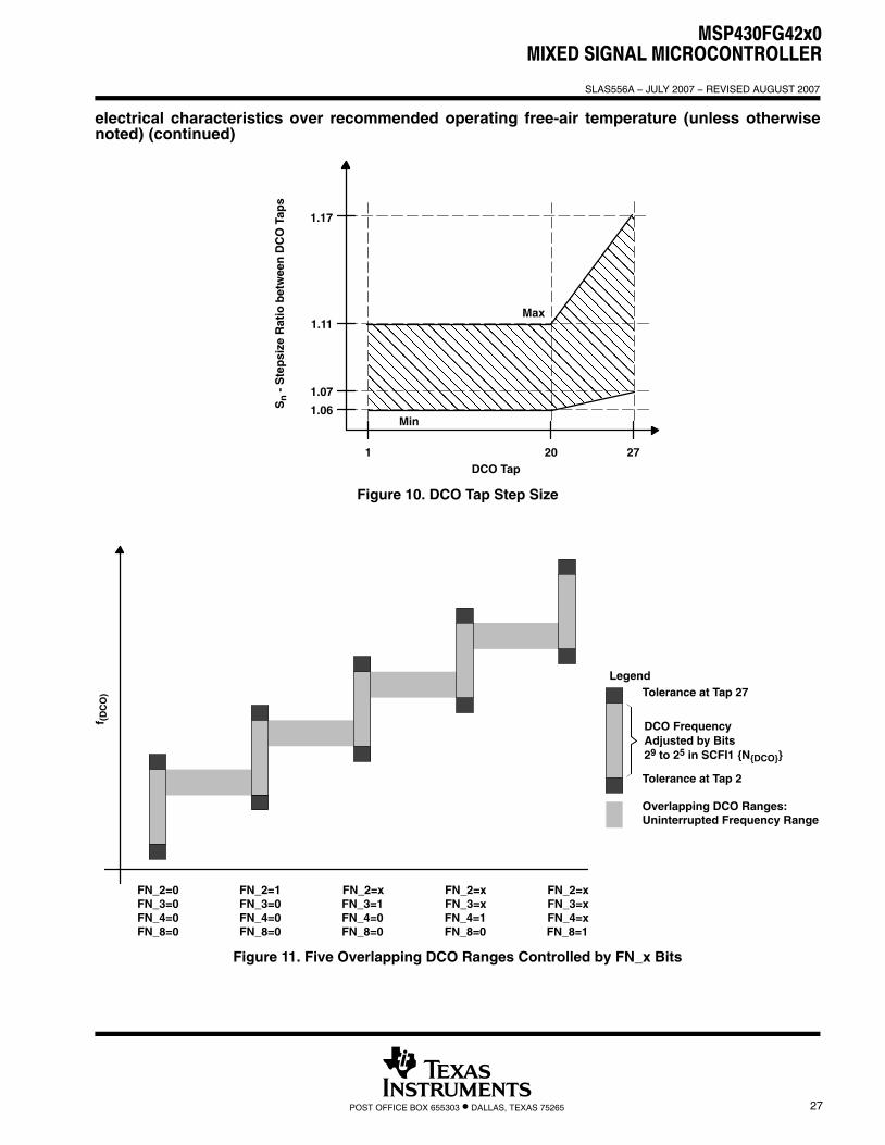
SStep size between adjacent DCO taps: 1 < TAP ≤ 20 1.06 1.11
SnStep size between adjacent DCO taps:Sn = fDCO(Tap n+1) / fDCO(Tap n) (see Figure 10 for taps 21 to 27) TAP = 27 1.07 1.17
DTemperature drift, N(DCO) = 01Eh, FN_8 = FN_4 = FN_3 = FN_2 = 0, 2.2 V –0.2 –0.3 –0.4
%/�CDtTemperature drift, N(DCO) = 01Eh, FN_8 = FN_4 = FN_3 = FN_2 = 0,D = 2, DCOPLUS = 0 (see Note 2) 3 V –0.2 –0.3 –0.4
%/�C
DVDrift with VCC variation, N(DCO) = 01Eh, FN_8 = FN_4 = FN_3 = FN_2 = 0, D = 2, DCOPLUS = 0
0 5 15 %/V
TA − °CVCC − V
f(DCO)f(DCO20�C)
f(DCO)f(DCO3V)
1.8 3.02.4 3.6
1.0
20 6040 85
1.0
0−20−400
Figure 9. DCO Frequency vs Supply Voltage VCC and vs Ambient Temperature
MSP430FG42x0MIXED SIGNAL MICROCONTROLLER
SLAS556A − JULY 2007 − REVISED AUGUST 2007
27POST OFFICE BOX 655303 • DALLAS, TEXAS 75265
electrical characteristics over recommended operating free-air temperature (unless otherwisenoted) (continued)
ÎÎÎÎÎÎÎÎÎÎÎÎÎÎÎÎÎÎÎÎÎÎÎÎÎÎÎÎÎÎÎÎÎÎÎÎÎÎÎÎÎÎÎÎÎÎÎÎÎÎÎÎÎÎÎÎÎÎÎÎÎÎÎÎÎÎÎÎÎÎÎÎÎÎÎÎÎÎÎÎÎÎÎÎÎÎÎÎÎÎÎÎÎÎÎÎÎÎÎÎÎÎÎÎÎÎÎÎÎÎÎÎÎÎÎÎÎÎÎÎÎÎÎÎÎÎÎÎÎÎ
1 2720
1.11
1.17
DCO Tap
Sn -
Ste
psi
ze R
atio
bet
wee
n D
CO
Tap
s
Min
Max
1.07
1.06
Figure 10. DCO Tap Step Size
DCO FrequencyAdjusted by Bits29 to 25 in SCFI1 {N{DCO}}
FN_2=0FN_3=0FN_4=0FN_8=0
FN_2=1FN_3=0FN_4=0FN_8=0
FN_2=xFN_3=1FN_4=0FN_8=0
FN_2=xFN_3=xFN_4=1FN_8=0
FN_2=xFN_3=xFN_4=xFN_8=1
LegendTolerance at Tap 27
Tolerance at Tap 2
Overlapping DCO Ranges:Uninterrupted Frequency Range
f (D
CO
)
Figure 11. Five Overlapping DCO Ranges Controlled by FN_x Bits

MSP430FG42x0MIXED SIGNAL MICROCONTROLLER
SLAS556A − JULY 2007 − REVISED AUGUST 2007
28 POST OFFICE BOX 655303 • DALLAS, TEXAS 75265
electrical characteristics over recommended operating free-air temperature (unless otherwisenoted)
crystal oscillator, LFXT1 oscillator (see Notes 1 and 2)PARAMETER TEST CONDITIONS MIN TYP MAX UNIT
OSCCAPx = 0h, VCC = 2.2 V / 3 V 0
CIntegrated input capacitance OSCCAPx = 1h, VCC = 2.2 V / 3 V 10
pFCXINIntegrated input capacitance(see Note 4) OSCCAPx = 2h, VCC = 2.2 V / 3 V 14
pF
OSCCAPx = 3h, VCC = 2.2 V / 3 V 18
OSCCAPx = 0h, VCC = 2.2 V / 3 V 0
CIntegrated output capacitance OSCCAPx = 1h, VCC = 2.2 V / 3 V 10
pFCXOUTIntegrated output capacitance(see Note 4) OSCCAPx = 2h, VCC = 2.2 V / 3 V 14
pF
OSCCAPx = 3h, VCC = 2.2 V / 3 V 18
VILInput levels at XIN V 2 2 V/3 V (see Note 3)
VSS 0.2×VCCV
VIHInput levels at XIN VCC = 2.2 V/3 V (see Note 3)
0.8×VCC VCCV
NOTES: 1. The parasitic capacitance from the package and board may be estimated to be 2 pF. The effective load capacitor for the crystal is(CXIN × CXOUT) / (CXIN + CXOUT). This is independent of XTS_FLL.
2. To improve EMI on the low-power LFXT1 oscillator, particularly in the LF mode (32 kHz), the following guidelines should be observed.− Keep as short of a trace as possible between the ’FG42x0 and the crystal.
− Design a good ground plane around the oscillator pins.
− Prevent crosstalk from other clock or data lines into oscillator pins XIN and XOUT.
− Avoid running PCB traces underneath or adjacent to the XIN and XOUT pins.
− Use assembly materials and praxis to avoid any parasitic load on the oscillator XIN and XOUT pins.
− If conformal coating is used, ensure that it does not induce capacitive/resistive leakage between the oscillator pins.
− Do not route the XOUT line to the JTAG header to support the serial programming adapter as shown in other
documentation. This signal is no longer required for the serial programming adapter.3. Applies only when using an external logic-level clock source. XTS_FLL must be set. Not applicable when using a crystal or
resonator.4. External capacitance is recommended for precision real-time clock applications, OSCCAPx = 0h.
MSP430FG42x0MIXED SIGNAL MICROCONTROLLER
SLAS556A − JULY 2007 − REVISED AUGUST 2007
29POST OFFICE BOX 655303 • DALLAS, TEXAS 75265
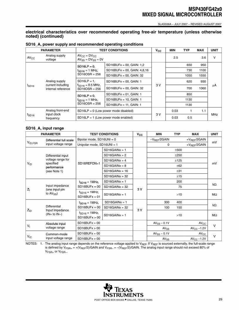
electrical characteristics over recommended operating free-air temperature (unless otherwisenoted) (continued)
SD16_A, power supply and recommended operating conditionsPARAMETER TEST CONDITIONS VCC MIN TYP MAX UNIT
AVCCAnalog supplyvoltage
AVCC = DVCCAVSS = DVSS = 0V
2.5 3.6 V
SD16LP = 0, SD16BUFx = 00, GAIN: 1,2 650 950SD16LP = 0,fSD16 = 1 MHz, SD16BUFx = 00, GAIN: 4,8,16 730 1100fSD16 1 MHz,SD16OSR = 256 SD16BUFx = 00, GAIN: 32 1050 1550
IAnalog supplycurrent including
SD16LP = 1,f 0 5 MHz
SD16BUFx = 00, GAIN: 13 V
620 930AISD16 current including
internal referencefSD16 = 0.5 MHz,SD16OSR = 256 SD16BUFx = 00, GAIN: 32
3 V700 1060
μA
SD16LP = 0, SD16BUFx = 01, GAIN: 1 850SD16LP = 0,fSD16 = 1 MHz, SD16BUFx = 10, GAIN: 1 1130fSD16 1 MHz,SD16OSR = 256 SD16BUFx = 11, GAIN: 1 1130
fAnalog front-endinput clock
SD16LP = 0 (Low power mode disabled)3 V
0.03 1 1.1MHzfSD16 input clock
frequency SD16LP = 1 (Low power mode enabled)3 V
0.03 0.5MHz
SD16_A, input rangePARAMETER TEST CONDITIONS VCC MIN TYP MAX UNIT
VDifferential full scale Bipolar mode, SD16UNI = 0 −VREF/2GAIN +VREF/2GAIN
mVVID,FSRDifferential full scaleinput voltage range Unipolar mode, SD16UNI = 1 0 +VREF/2GAIN
mV
SD16GAINx = 1 ±500
Differential input SD16GAINx = 2 ±250
V
Differential inputvoltage range forspecified SD16REFON 1
SD16GAINx = 4 ±125mVVID specified
performanceSD16REFON=1
SD16GAINx = 8 ±62mV
performance(see Note 1) SD16GAINx = 16 ±31(see Note 1)
SD16GAINx = 32 ±15
fSD16 = 1MHz, SD16GAINx = 1 200kΩ
ZInput impedance(one input pin
fSD16 1MHz,
SD16BUFx = 00 SD16GAINx = 323 V
75kΩ
ZI (one input pinto AVSS) fSD16 = 1MHz,
SD16BUFx = 01SD16GAINx = 1
3 V
>10 MΩ
fSD16 = 1MHz, SD16GAINx = 1 300 400kΩ
ZDifferential Input impedance
fSD16 1MHz,
SD16BUFx = 00 SD16GAINx = 323 V
100 150kΩ
ZID Input impedance(IN+ to IN−) fSD16 = 1MHz,
SD16BUFx > 00SD16GAINx = 1
3 V
>10 MΩ
VAbsolute input SD16BUFx = 00 AVSS − 0.1V AVCC
VVIAbsolute inputvoltage range SD16BUFx > 00 AVSS AVCC −1.2V
V
VCommon-mode SD16BUFx = 00 AVSS − 0.1V AVCC
VVICCommon modeinput voltage range SD16BUFx > 00 AVSS AVCC −1.2V
V
NOTES: 1. The analog input range depends on the reference voltage applied to VREF. If VREF is sourced externally, the full-scale rangeis defined by VFSR+ = +(VREF/2)/GAIN and VFSR− = −(VREF/2)/GAIN. The analog input range should not exceed 80% ofVFSR+ or VFSR−.
MSP430FG42x0MIXED SIGNAL MICROCONTROLLER
SLAS556A − JULY 2007 − REVISED AUGUST 2007
30 POST OFFICE BOX 655303 • DALLAS, TEXAS 75265
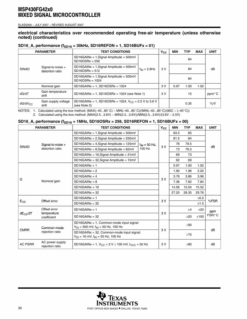
electrical characteristics over recommended operating free-air temperature (unless otherwisenoted) (continued)
SD16_A, performance (fSD16 = 30kHz, SD16REFON = 1, SD16BUFx = 01)PARAMETER TEST CONDITIONS VCC MIN TYP MAX UNIT
SD16GAINx = 1,Signal Amplitude = 500mVSD16OSRx = 256
84
SINADSignal-to-noise +distortion ratio
SD16GAINx = 1,Signal Amplitude = 500mVSD16OSRx = 512 fIN = 2.8Hz 3 V 84 dB
distortion ratio
SD16GAINx = 1,Signal Amplitude = 500mVSD16OSRx = 1024
84
Nominal gain SD16GAINx = 1, SD16OSRx = 1024 3 V 0.97 1.00 1.02
dG/dTGain temperaturedrift
SD16GAINx = 1, SD16OSRx = 1024 (see Note 1) 3 V 15 ppm/�C
dG/dVCCGain supply voltagedrift
SD16GAINx = 1, SD16OSRx = 1024, VCC = 2.5 V to 3.6 V(see Note 2)
0.35 %/V
NOTES: 1. Calculated using the box method: (MAX(−40...85�C) − MIN(−40...85�C))/MIN(−40...85�C)/(85C − (−40�C))2. Calculated using the box method: (MAX(2.5...3.6V) − MIN(2.5...3.6V))/MIN(2.5...3.6V)/(3.6V − 2.5V)
SD16_A, performance (fSD16 = 1MHz, SD16OSRx = 256, SD16REFON = 1, SD16BUFx = 00)PARAMETER TEST CONDITIONS VCC MIN TYP MAX UNIT
SD16GAINx = 1,Signal Amplitude = 500mV 83.5 85
SD16GAINx = 2,Signal Amplitude = 250mV 81.5 84
SINADSignal-to-noise + SD16GAINx = 4,Signal Amplitude = 125mV fIN = 50 Hz,
3 V76 79.5
dBSINADSignal to noise +distortion ratio SD16GAINx = 8,Signal Amplitude = 62mV
fIN = 50 Hz,100 Hz 3 V
73 76.5dB
SD16GAINx = 16,Signal Amplitude = 31mV 69 73
SD16GAINx = 32,Signal Amplitude = 15mV 62 69
SD16GAINx = 1 0.97 1.00 1.02
SD16GAINx = 2 1.90 1.96 2.02
GSD16GAINx = 4
3 V3.76 3.86 3.96
G Nominal gain SD16GAINx = 83 V
7.36 7.62 7.84
SD16GAINx = 16 14.56 15.04 15.52
SD16GAINx = 32 27.20 28.35 29.76
E Offset errorSD16GAINx = 1
3 V±0.2
%FSREOS Offset errorSD16GAINx = 32
3 V±1.5
%FSR
dE /dTOffset errortemperature
SD16GAINx = 13 V
±4 ±20 ppmdEOS/dT temperature
coefficient SD16GAINx = 323 V
±20 ±100
ppmFSR/�C
CMRRCommon-mode
SD16GAINx = 1, Common-mode input signal:VID = 500 mV, fIN = 50 Hz, 100 Hz
3 V
>90
dBCMRRCommon moderejection ratio SD16GAINx = 32, Common-mode input signal:
VID = 16 mV, fIN = 50 Hz, 100 Hz
3 V>75
dB
AC PSRRAC power supplyrejection ratio
SD16GAINx = 1, VCC = 3 V ± 100 mV, fVCC = 50 Hz 3 V >80 dB
MSP430FG42x0MIXED SIGNAL MICROCONTROLLER
SLAS556A − JULY 2007 − REVISED AUGUST 2007
31POST OFFICE BOX 655303 • DALLAS, TEXAS 75265
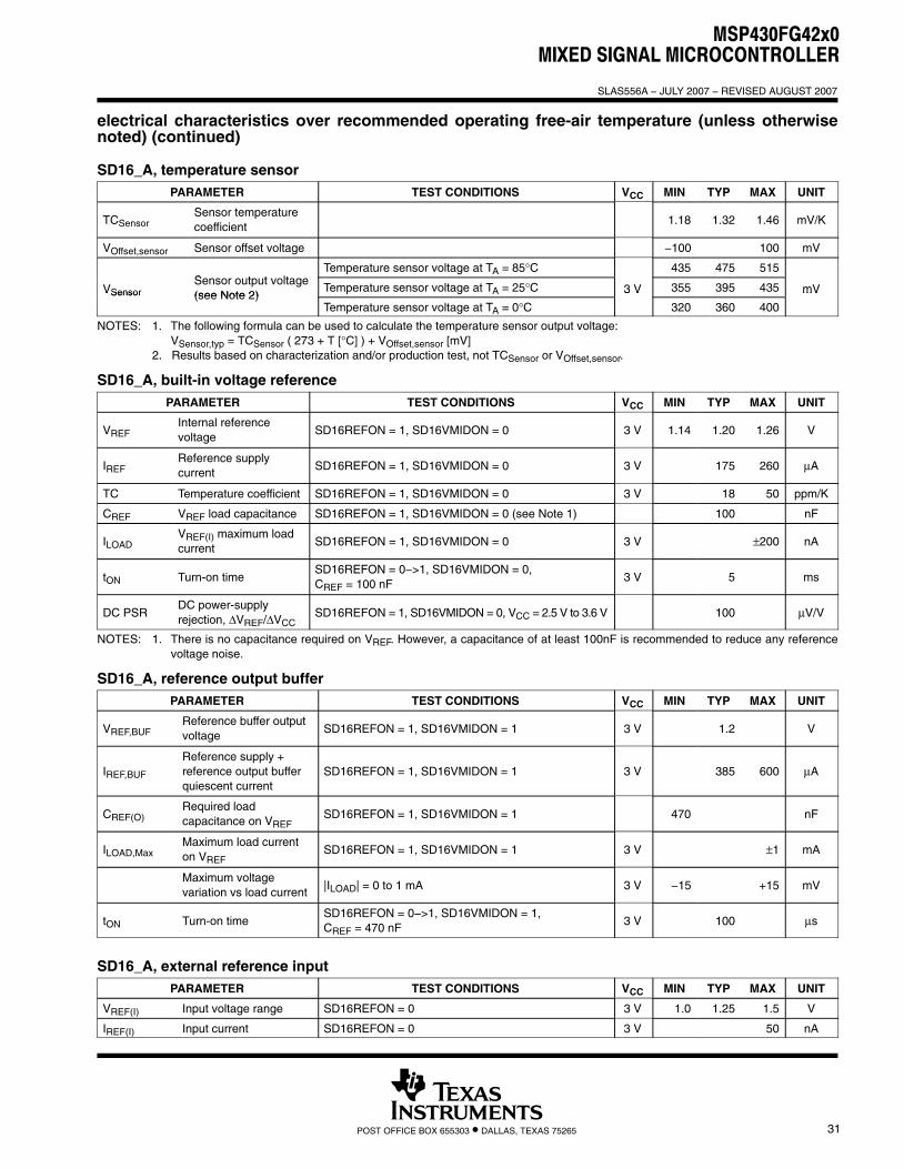
electrical characteristics over recommended operating free-air temperature (unless otherwisenoted) (continued)
SD16_A, temperature sensorPARAMETER TEST CONDITIONS VCC MIN TYP MAX UNIT
TCSensorSensor temperaturecoefficient
1.18 1.32 1.46 mV/K
VOffset,sensor Sensor offset voltage −100 100 mV
S t t ltTemperature sensor voltage at TA = 85°C 435 475 515
VSensorSensor output voltage(see Note 2)
Temperature sensor voltage at TA = 25°C 3 V 355 395 435 mVVSensor (see Note 2)Temperature sensor voltage at TA = 0°C
3 V
320 360 400
mV
NOTES: 1. The following formula can be used to calculate the temperature sensor output voltage:VSensor,typ = TCSensor ( 273 + T [°C] ) + VOffset,sensor [mV]
2. Results based on characterization and/or production test, not TCSensor or VOffset,sensor.
SD16_A, built-in voltage referencePARAMETER TEST CONDITIONS VCC MIN TYP MAX UNIT
VREFInternal referencevoltage
SD16REFON = 1, SD16VMIDON = 0 3 V 1.14 1.20 1.26 V
IREFReference supplycurrent
SD16REFON = 1, SD16VMIDON = 0 3 V 175 260 μA
TC Temperature coefficient SD16REFON = 1, SD16VMIDON = 0 3 V 18 50 ppm/K
CREF VREF load capacitance SD16REFON = 1, SD16VMIDON = 0 (see Note 1) 100 nF
ILOADVREF(I) maximum loadcurrent
SD16REFON = 1, SD16VMIDON = 0 3 V ±200 nA
tON Turn-on timeSD16REFON = 0−>1, SD16VMIDON = 0,CREF = 100 nF
3 V 5 ms
DC PSRDC power-supplyrejection, ΔVREF/ΔVCC
SD16REFON = 1, SD16VMIDON = 0, VCC = 2.5 V to 3.6 V 100 μV/V
NOTES: 1. There is no capacitance required on VREF. However, a capacitance of at least 100nF is recommended to reduce any referencevoltage noise.
SD16_A, reference output bufferPARAMETER TEST CONDITIONS VCC MIN TYP MAX UNIT
VREF,BUFReference buffer outputvoltage
SD16REFON = 1, SD16VMIDON = 1 3 V 1.2 V
IREF,BUF
Reference supply +reference output bufferquiescent current
SD16REFON = 1, SD16VMIDON = 1 3 V 385 600 μA
CREF(O)Required loadcapacitance on VREF
SD16REFON = 1, SD16VMIDON = 1 470 nF
ILOAD,MaxMaximum load currenton VREF
SD16REFON = 1, SD16VMIDON = 1 3 V ±1 mA
Maximum voltagevariation vs load current
|ILOAD| = 0 to 1 mA 3 V −15 +15 mV
tON Turn-on timeSD16REFON = 0−>1, SD16VMIDON = 1,CREF = 470 nF
3 V 100 μs
SD16_A, external reference inputPARAMETER TEST CONDITIONS VCC MIN TYP MAX UNIT
VREF(I) Input voltage range SD16REFON = 0 3 V 1.0 1.25 1.5 V
IREF(I) Input current SD16REFON = 0 3 V 50 nA
MSP430FG42x0MIXED SIGNAL MICROCONTROLLER
SLAS556A − JULY 2007 − REVISED AUGUST 2007
32 POST OFFICE BOX 655303 • DALLAS, TEXAS 75265
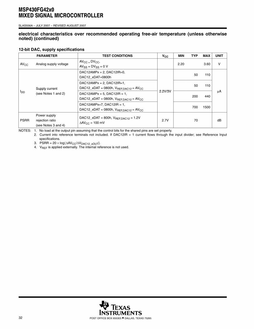
electrical characteristics over recommended operating free-air temperature (unless otherwisenoted) (continued)
12-bit DAC, supply specificationsPARAMETER TEST CONDITIONS VCC MIN TYP MAX UNIT
AVCC Analog supply voltageAVCC = DVCC,
AVSS = DVSS = 0 V2.20 3.60 V
DAC12AMPx = 2, DAC12IR=0,
DAC12_xDAT=0800h50 110
ISupply current
DAC12AMPx = 2, DAC12IR=1,
DAC12_xDAT = 0800h, VREF,DAC12 = AVCC2 2V/3V
50 110
AIDDSupply current
(see Notes 1 and 2) DAC12AMPx = 5, DAC12IR = 1,
DAC12_xDAT = 0800h, VREF,DAC12 = AVCC
2.2V/3V
200 440
μA
DAC12AMPx=7, DAC12IR = 1,
DAC12_xDAT = 0800h, VREF,DAC12 = AVCC700 1500
PSRR
Power supply
rejection ratio
(see Notes 3 and 4)
DAC12_xDAT = 800h, VREF,DAC12 = 1.2V
ΔAVCC = 100 mV2.7V 70 dB
NOTES: 1. No load at the output pin assuming that the control bits for the shared pins are set properly.2. Current into reference terminals not included. If DAC12IR = 1 current flows through the input divider; see Reference Input
specifications.3. PSRR = 20 × log{ΔAVCC/ΔVDAC12_xOUT}.4. VREF is applied externally. The internal reference is not used.
MSP430FG42x0MIXED SIGNAL MICROCONTROLLER
SLAS556A − JULY 2007 − REVISED AUGUST 2007
33POST OFFICE BOX 655303 • DALLAS, TEXAS 75265
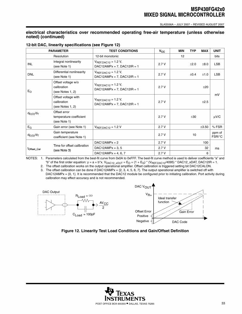
electrical characteristics over recommended operating free-air temperature (unless otherwisenoted) (continued)
12-bit DAC, linearity specifications (see Figure 12)PARAMETER TEST CONDITIONS VCC MIN TYP MAX UNIT
Resolution 12-bit monotonic 12 bits
INLIntegral nonlinearity
(see Note 1)
VREF,DAC12 = 1.2 V,
DAC12AMPx = 7, DAC12IR = 12.7 V ±2.0 ±8.0 LSB
DNLDifferential nonlinearity
(see Note 1)
VREF,DAC12 = 1.2 V,
DAC12AMPx = 7, DAC12IR = 12.7 V ±0.4 ±1.0 LSB
EO
Offset voltage w/o
calibration
(see Notes 1, 2)
VREF,DAC12 = 1.2 V,
DAC12AMPx = 7, DAC12IR = 12.7 V ±20
mVOffset voltage with
calibration
(see Notes 1, 2)
VREF,DAC12 = 1.2 V,
DAC12AMPx = 7, DAC12IR = 12.7 V ±2.5
mV
dE(O)/dTOffset error
temperature coefficient
(see Note 1)
2.7 V ±30 μV/C
EG Gain error (see Note 1) VREF,DAC12 = 1.2 V 2.7 V ±3.50 % FSR
dE(G)/dTGain temperature
coefficient (see Note 1)2.7 V 10
ppm ofFSR/°C
Time for offset calibrationDAC12AMPx = 2 2.7 V 100
tOffset_CalTime for offset calibration
(see Note 3)DAC12AMPx = 3, 5 2.7 V 32 mstOffset_Cal (see Note 3)DAC12AMPx = 4, 6, 7 2.7 V 6
ms
NOTES: 1. Parameters calculated from the best-fit curve from 0x0A to 0xFFF. The best-fit curve method is used to deliver coefficients “a” and“b” of the first order equation: y = a + b*x. VDAC12_xOUT = EO + (1 + EG) * (VREF,DAC12/4095) * DAC12_xDAT, DAC12IR = 1.
2. The offset calibration works on the output operational amplifier. Offset calibration is triggered setting bit DAC12CALON.3. The offset calibration can be done if DAC12AMPx = {2, 3, 4, 5, 6, 7}. The output operational amplifier is switched off with
DAC12AMPx = {0, 1}. It is recommended that the DAC12 module be configured prior to initiating calibration. Port activity duringcalibration may effect accuracy and is not recommended.
Positive
Negative
VR+
Gain ErrorOffset Error
DAC Code
DAC VOUT
Ideal transferfunction
RLoad =
AVCC
CLoad = 100pF
2
DAC Output
Figure 12. Linearity Test Load Conditions and Gain/Offset Definition
MSP430FG42x0MIXED SIGNAL MICROCONTROLLER
SLAS556A − JULY 2007 − REVISED AUGUST 2007
34 POST OFFICE BOX 655303 • DALLAS, TEXAS 75265
electrical characteristics over recommended operating free-air temperature (unless otherwisenoted) (continued)
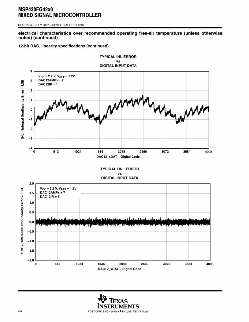
12-bit DAC, linearity specifications (continued)
DAC12_xDAT − Digital Code
−4
−3
−2
−1
0
1
2
3
4
0 512 1024 1536 2048 2560 3072 3584
VCC = 2.2 V, VREF = 1.2VDAC12AMPx = 7DAC12IR = 1
TYPICAL INL ERRORvs
DIGITAL INPUT DATA
4095
INL
− In
teg
ral N
on
linea
rity
Err
or
− L
SB
DAC12_xDAT − Digital Code
−2.0
−1.5
−1.0
−0.5
0.0
0.5
1.0
1.5
2.0
0 512 1024 1536 2048 2560 3072 3584
VCC = 2.2 V, VREF = 1.2VDAC12AMPx = 7DAC12IR = 1
TYPICAL DNL ERRORvs
DIGITAL INPUT DATA
4095
DN
L −
Dif
fere
nti
al N
on
linea
rity
Err
or
− L
SB
MSP430FG42x0MIXED SIGNAL MICROCONTROLLER
SLAS556A − JULY 2007 − REVISED AUGUST 2007
35POST OFFICE BOX 655303 • DALLAS, TEXAS 75265
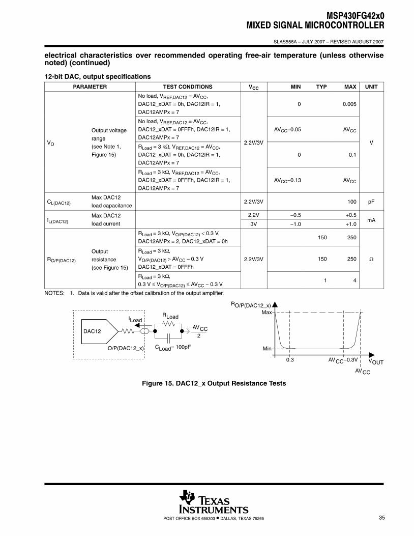
electrical characteristics over recommended operating free-air temperature (unless otherwisenoted) (continued)
12-bit DAC, output specificationsPARAMETER TEST CONDITIONS VCC MIN TYP MAX UNIT
No load, VREF,DAC12 = AVCC,
DAC12_xDAT = 0h, DAC12IR = 1,
DAC12AMPx = 7
0 0.005
V
Output voltage
range
No load, VREF,DAC12 = AVCC,
DAC12_xDAT = 0FFFh, DAC12IR = 1,
DAC12AMPx = 72 2V/3V
AVCC−0.05 AVCC
VVOrange
(see Note 1,
Figure 15)
RLoad = 3 kΩ, VREF,DAC12 = AVCC,
DAC12_xDAT = 0h, DAC12IR = 1,
DAC12AMPx = 7
2.2V/3V
0 0.1
V
RLoad = 3 kΩ, VREF,DAC12 = AVCC,
DAC12_xDAT = 0FFFh, DAC12IR = 1,
DAC12AMPx = 7
AVCC−0.13 AVCC
CL(DAC12)Max DAC12
load capacitance 2.2V/3V 100 pF
IMax DAC12 2.2V −0.5 +0.5
mAIL(DAC12)Max DAC12
load current
3V −1.0 +1.0mA
RLoad = 3 kΩ, VO/P(DAC12) < 0.3 V,
DAC12AMPx = 2, DAC12_xDAT = 0h150 250
RO/P(DAC12)
Output
resistance
(see Figure 15)
RLoad = 3 kΩ,
VO/P(DAC12) > AVCC – 0.3 V
DAC12_xDAT = 0FFFh2.2V/3V 150 250 Ω
(see Figure 15)
RLoad = 3 kΩ,
0.3 V ≤ VO/P(DAC12) ≤ AVCC − 0.3 V1 4
NOTES: 1. Data is valid after the offset calibration of the output amplifier.
RO/P(DAC12_x)Max
0.3
AVCC
AVCC −0.3V VOUT
Min
RLoad
AVCC
CLoad = 100pF
2
ILoad
DAC12
O/P(DAC12_x)
Figure 15. DAC12_x Output Resistance Tests
MSP430FG42x0MIXED SIGNAL MICROCONTROLLER
SLAS556A − JULY 2007 − REVISED AUGUST 2007
36 POST OFFICE BOX 655303 • DALLAS, TEXAS 75265
electrical characteristics over recommended operating free-air temperature (unless otherwisenoted)
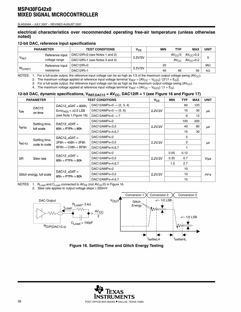
12-bit DAC, reference input specificationsPARAMETER TEST CONDITIONS VCC MIN TYP MAX UNIT
VReference input DAC12IR=0 (see Notes 1 and 2)
2 2V/3V AVCC/3 AVCC+0.2
VVREFReference input
voltage range DAC12IR=1 (see Notes 3 and 4)2.2V/3V
AVCC AVCC+0.2V
RiReference input DAC12IR=0
2 2V/3V20 MΩ
Ri(VREF)Reference input
resistance DAC12IR=12.2V/3V
40 48 56 kΩNOTES: 1. For a full-scale output, the reference input voltage can be as high as 1/3 of the maximum output voltage swing (AVCC).
2. The maximum voltage applied at reference input voltage terminal VREF = [AVCC − VE(O)] / [3*(1 + EG)].3. For a full-scale output, the reference input voltage can be as high as the maximum output voltage swing (AVCC).4. The maximum voltage applied at reference input voltage terminal VREF = [AVCC − VE(O)] / (1 + EG).
12-bit DAC, dynamic specifications, VREF,DAC12 = AVCC, DAC12IR = 1 (see Figure 16 and Figure 17)PARAMETER TEST CONDITIONS VCC MIN TYP MAX UNIT
DAC12DAC12_xDAT = 800h, DAC12AMPx=0 → {2, 3, 4} 60 120
tONDAC12
on time
DAC12_xDAT = 800h,
ErrorV(O) < ±0.5 LSB DAC12AMPx=0 → {5, 6} 2.2V/3V 15 30 μstON on timeErrorV(O) < ±0.5 LSB
(see Note 1,Figure 16) DAC12AMPx=0 → 7
2.2V/3V
6 12
μs
Settling time DAC12 xDATDAC12AMPx=2 100 200
tS(FS)Settling time,
full scale
DAC12_xDAT =
80h→ F7Fh→ 80hDAC12AMPx=3,5 2.2V/3V 40 80 μstS(FS) full scale 80h→ F7Fh→ 80hDAC12AMPx=4,6,7
2.2V/3V
15 30
μs
Settling timeDAC12_xDAT = DAC12AMPx=2 5
tS(C-C)Settling time,
code to code
DAC12_xDAT =
3F8h→ 408h→ 3F8h DAC12AMPx=3,5 2.2V/3V 2 μstS(C-C) code to code3F8h→ 408h→ 3F8h
BF8h→ C08h→ BF8h DAC12AMPx=4,6,7
2.2V/3V
1
μs
DAC12 xDATDAC12AMPx=2 0.05 0.12
SR Slew rateDAC12_xDAT =
80h→ F7Fh→ 80hDAC12AMPx=3,5 2.2V/3V 0.35 0.7 V/μsSR Slew rate
80h→ F7Fh→ 80hDAC12AMPx=4,6,7
2.2V/3V
1.5 2.7
V/μs
DAC12 xDATDAC12AMPx=2 10
Glitch energy, full scaleDAC12_xDAT =
80h→ F7Fh→ 80hDAC12AMPx=3,5 2.2V/3V 10 nV-sGlitch energy, full scale
80h→ F7Fh→ 80hDAC12AMPx=4,6,7
2.2V/3V
15
nV s
NOTES: 1. RLoad and CLoad connected to AVSS (not AVCC/2) in Figure 16.2. Slew rate applies to output voltage steps ≥ 200mV.
RLoad
AVCC
CLoad = 100pF
2
DAC Output
RO/P(DAC12.x)
ILoad
Conversion 1 Conversion 2
VOUT
Conversion 3
GlitchEnergy
+/− 1/2 LSB
+/− 1/2 LSB
tsettleLH tsettleHL
= 3 kΩ
Figure 16. Settling Time and Glitch Energy Testing
MSP430FG42x0MIXED SIGNAL MICROCONTROLLER
SLAS556A − JULY 2007 − REVISED AUGUST 2007
37POST OFFICE BOX 655303 • DALLAS, TEXAS 75265
electrical characteristics over recommended operating free-air temperature (unless otherwisenoted)
Conversion 1 Conversion 2
VOUT
Conversion 3
10%
tSRLH tSRHL
90%
10%
90%
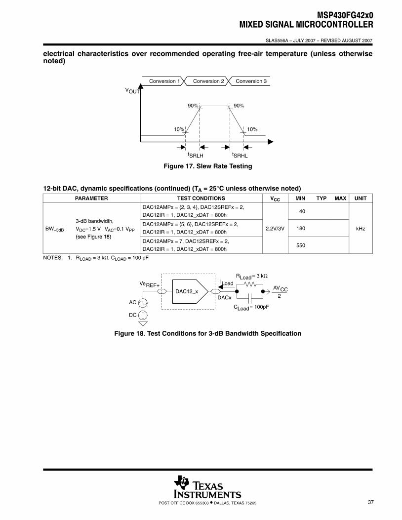
Figure 17. Slew Rate Testing
12-bit DAC, dynamic specifications (continued) (TA = 25°C unless otherwise noted)PARAMETER TEST CONDITIONS VCC MIN TYP MAX UNIT
3 dB b d idth
DAC12AMPx = {2, 3, 4}, DAC12SREFx = 2,
DAC12IR = 1, DAC12_xDAT = 800h40
BW−3dB
3-dB bandwidth,
VDC=1.5 V, VAC=0.1 VPP
(see Figure 18)
DAC12AMPx = {5, 6}, DAC12SREFx = 2,
DAC12IR = 1, DAC12_xDAT = 800h2.2V/3V 180 kHz
(see Figure 18)DAC12AMPx = 7, DAC12SREFx = 2,
DAC12IR = 1, DAC12_xDAT = 800h550
NOTES: 1. RLOAD = 3 kΩ, CLOAD = 100 pF
VeREF+
AC
DC
RLoad
AVCC
CLoad = 100pF
2
ILoad
DAC12_xDACx
= 3 kΩ
Figure 18. Test Conditions for 3-dB Bandwidth Specification
MSP430FG42x0MIXED SIGNAL MICROCONTROLLER
SLAS556A − JULY 2007 − REVISED AUGUST 2007
38 POST OFFICE BOX 655303 • DALLAS, TEXAS 75265
electrical characteristics over recommended operating free-air temperature (unless otherwisenoted)
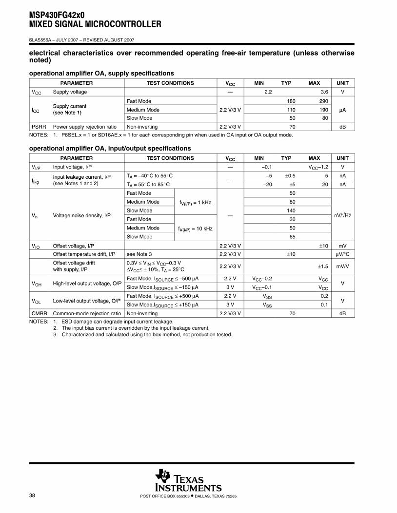
operational amplifier OA, supply specificationsPARAMETER TEST CONDITIONS VCC MIN TYP MAX UNIT
VCC Supply voltage — 2.2 3.6 V
Fast Mode 180 290S l t
Fast Mode 180 290
ISupply current
Medium Mode 2 2 V/3 V 110 190 AICCSupply current(see Note 1) Medium Mode 2.2 V/3 V 110 190 μAICC (see Note 1)
Slow Mode
2.2 V/3 V
50 80
μA
PSRR Power supply rejection ratio Non-inverting 2.2 V/3 V 70 dB
NOTES: 1. P6SEL.x = 1 or SD16AE.x = 1 for each corresponding pin when used in OA input or OA output mode.
operational amplifier OA, input/output specificationsPARAMETER TEST CONDITIONS VCC MIN TYP MAX UNIT
VI/P Input voltage, I/P — −0.1 VCC−1.2 V
IInput leakage current, I/P TA = −40�C to 55�C −5 ±0.5 5 nA
IIkgInput leakage current, I/P(see Notes 1 and 2) TA = 55�C to 85�C
—−20 ±5 20 nA
Fast Mode 50
Medium Mode fV(I/P) = 1 kHz 80
V Voltage noise density I/PSlow Mode
fV(I/P) 1 kHz
140nV/√HzVn Voltage noise density, I/P
Fast Mode—
30nV/√Hz
Medium Mode fV(I/P) = 10 kHz 50
Slow Mode
fV(I/P) 10 kHz
65
V Offset voltage I/P 2 2 V/3 V ±10 mVVIO Offset voltage, I/P 2.2 V/3 V ±10 mV
Offset temperature drift, I/P see Note 3 2.2 V/3 V ±10 μV/°C
Offset voltage driftwith supply, I/P
0.3V ≤ VIN ≤ VCC−0.3 VΔVCC≤ ± 10%, TA = 25°C 2.2 V/3 V ±1.5 mV/V
V High level output voltage O/PFast Mode, ISOURCE ≤ −500 μA 2.2 V VCC−0.2 VCC
VVOH High-level output voltage, O/PSlow Mode,ISOURCE ≤ −150 μA 3 V VCC−0.1 VCC
V
V Low level output voltage O/PFast Mode, ISOURCE ≤ +500 μA 2.2 V VSS 0.2
VVOL Low-level output voltage, O/PSlow Mode,ISOURCE ≤ +150 μA 3 V VSS 0.1
V
CMRR Common-mode rejection ratio Non-inverting 2.2 V/3 V 70 dB
NOTES: 1. ESD damage can degrade input current leakage.2. The input bias current is overridden by the input leakage current.3. Characterized and calculated using the box method, not production tested.
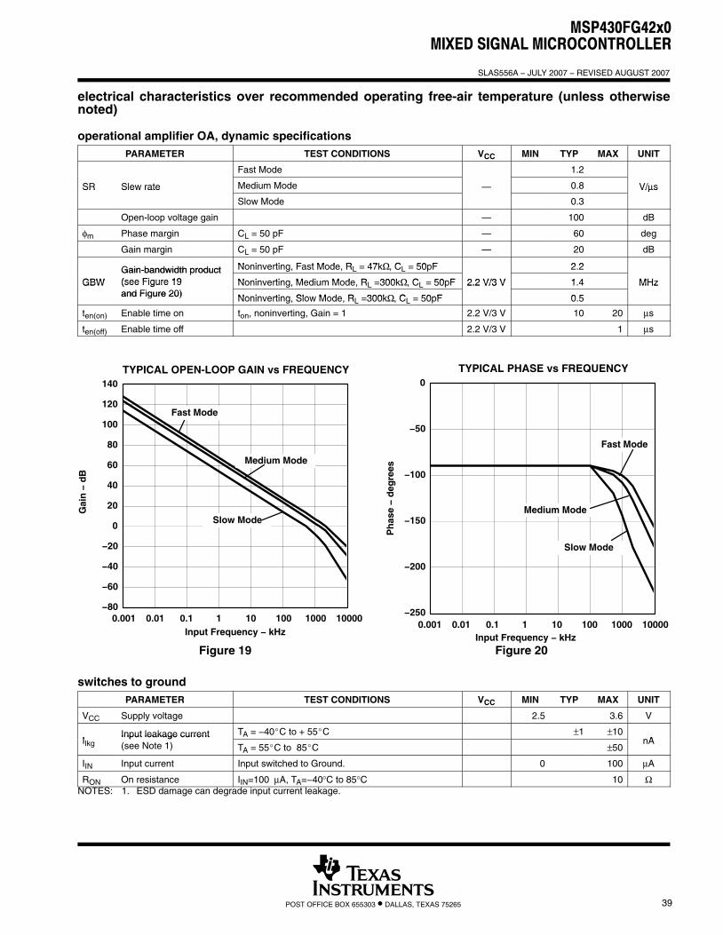
MSP430FG42x0MIXED SIGNAL MICROCONTROLLER
SLAS556A − JULY 2007 − REVISED AUGUST 2007
39POST OFFICE BOX 655303 • DALLAS, TEXAS 75265
electrical characteristics over recommended operating free-air temperature (unless otherwisenoted)
operational amplifier OA, dynamic specificationsPARAMETER TEST CONDITIONS VCC MIN TYP MAX UNIT
Fast Mode 1.2
SR Slew rate Medium Mode — 0.8 V/μsSR Slew rate
Slow Mode 0.3
V/μs
Open-loop voltage gain — 100 dB
φm Phase margin CL = 50 pF — 60 deg
Gain margin CL = 50 pF — 20 dB
Noninverting Fast Mode R 47kΩ C 50pF 2 2Gain-bandwidth product Noninverting, Fast Mode, RL = 47kΩ, CL = 50pF 2.2
GBWGain-bandwidth product(see Figure 19 Noninverting Medium Mode R 300kΩ C 50pF 2 2 V/3 V 1 4 MHzGBW (see Figure 19 Noninverting, Medium Mode, RL =300kΩ, CL = 50pF 2.2 V/3 V 1.4 MHzGBW (see Figure 19and Figure 20) Noninverting Slow Mode R 300kΩ C 50pF
2.2 V/3 V
0 5
MHzand Figure 20) Noninverting, Slow Mode, RL =300kΩ, CL = 50pF 0.5
ten(on) Enable time on ton, noninverting, Gain = 1 2.2 V/3 V 10 20 μs
ten(off) Enable time off 2.2 V/3 V 1 μs
Figure 19
Input Frequency − kHz
−80
−60
−40
−20
0
20
40
60
80
100
120
140TYPICAL OPEN-LOOP GAIN vs FREQUENCY
Slow Mode
Fast Mode
Gai
n −
dB
Medium Mode
0.001 0.01 0.1 1 10 100 1000 10000
Figure 20Input Frequency − kHz
−250
−200
−150
−100
−50
0TYPICAL PHASE vs FREQUENCY
Ph
ase
− d
egre
es
Slow Mode
Fast Mode
Medium Mode
0.001 0.01 0.1 1 10 100 1000 10000
switches to groundPARAMETER TEST CONDITIONS VCC MIN TYP MAX UNIT
VCC Supply voltage 2.5 3.6 V
IInput leakage current TA = −40�C to + 55�C ±1 ±10
nAIlkgInput leakage current(see Note 1) TA = 55�C to 85�C ±50
nA
IIN Input current Input switched to Ground. 0 100 μA
RON On resistance IIN=100 μA, TA=−40°C to 85°C 10 ΩNOTES: 1. ESD damage can degrade input current leakage.
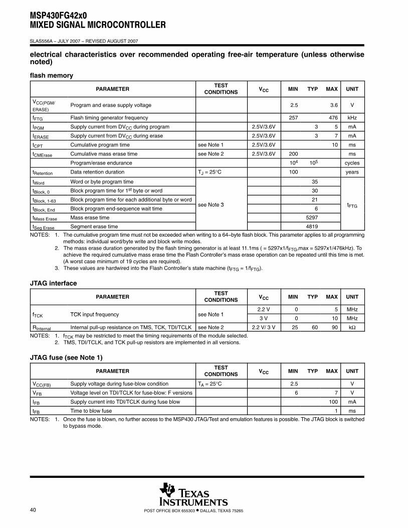
MSP430FG42x0MIXED SIGNAL MICROCONTROLLER
SLAS556A − JULY 2007 − REVISED AUGUST 2007
40 POST OFFICE BOX 655303 • DALLAS, TEXAS 75265
electrical characteristics over recommended operating free-air temperature (unless otherwisenoted)
flash memory
PARAMETERTEST
CONDITIONS VCC MIN TYP MAX UNIT
VCC(PGM/
ERASE)Program and erase supply voltage 2.5 3.6 V
fFTG Flash timing generator frequency 257 476 kHz
IPGM Supply current from DVCC during program 2.5V/3.6V 3 5 mA
IERASE Supply current from DVCC during erase 2.5V/3.6V 3 7 mA
tCPT Cumulative program time see Note 1 2.5V/3.6V 10 ms
tCMErase Cumulative mass erase time see Note 2 2.5V/3.6V 200 ms
Program/erase endurance 104 105 cycles
tRetention Data retention duration TJ = 25°C 100 years
tWord Word or byte program time 35
tBlock, 0 Block program time for 1st byte or word 30
tBlock, 1-63 Block program time for each additional byte or wordsee Note 3
21t
tBlock, End Block program end-sequence wait timesee Note 3
6tFTG
tMass Erase Mass erase time 5297
tSeg Erase Segment erase time 4819
NOTES: 1. The cumulative program time must not be exceeded when writing to a 64−byte flash block. This parameter applies to all programmingmethods: individual word/byte write and block write modes.
2. The mass erase duration generated by the flash timing generator is at least 11.1ms ( = 5297x1/fFTG,max = 5297x1/476kHz). Toachieve the required cumulative mass erase time the Flash Controller’s mass erase operation can be repeated until this time is met.(A worst case minimum of 19 cycles are required).
3. These values are hardwired into the Flash Controller’s state machine (tFTG = 1/fFTG).
JTAG interface
PARAMETERTEST
CONDITIONS VCC MIN TYP MAX UNIT
f TCK input frequency see Note 12.2 V 0 5 MHz
fTCK TCK input frequency see Note 13 V 0 10 MHz
RInternal Internal pull-up resistance on TMS, TCK, TDI/TCLK see Note 2 2.2 V/ 3 V 25 60 90 kΩNOTES: 1. fTCK may be restricted to meet the timing requirements of the module selected.
2. TMS, TDI/TCLK, and TCK pull-up resistors are implemented in all versions.
JTAG fuse (see Note 1)
PARAMETERTEST
CONDITIONS VCC MIN TYP MAX UNIT
VCC(FB) Supply voltage during fuse-blow condition TA = 25°C 2.5 V
VFB Voltage level on TDI/TCLK for fuse-blow: F versions 6 7 V
IFB Supply current into TDI/TCLK during fuse blow 100 mA
tFB Time to blow fuse 1 ms
NOTES: 1. Once the fuse is blown, no further access to the MSP430 JTAG/Test and emulation features is possible. The JTAG block is switchedto bypass mode.
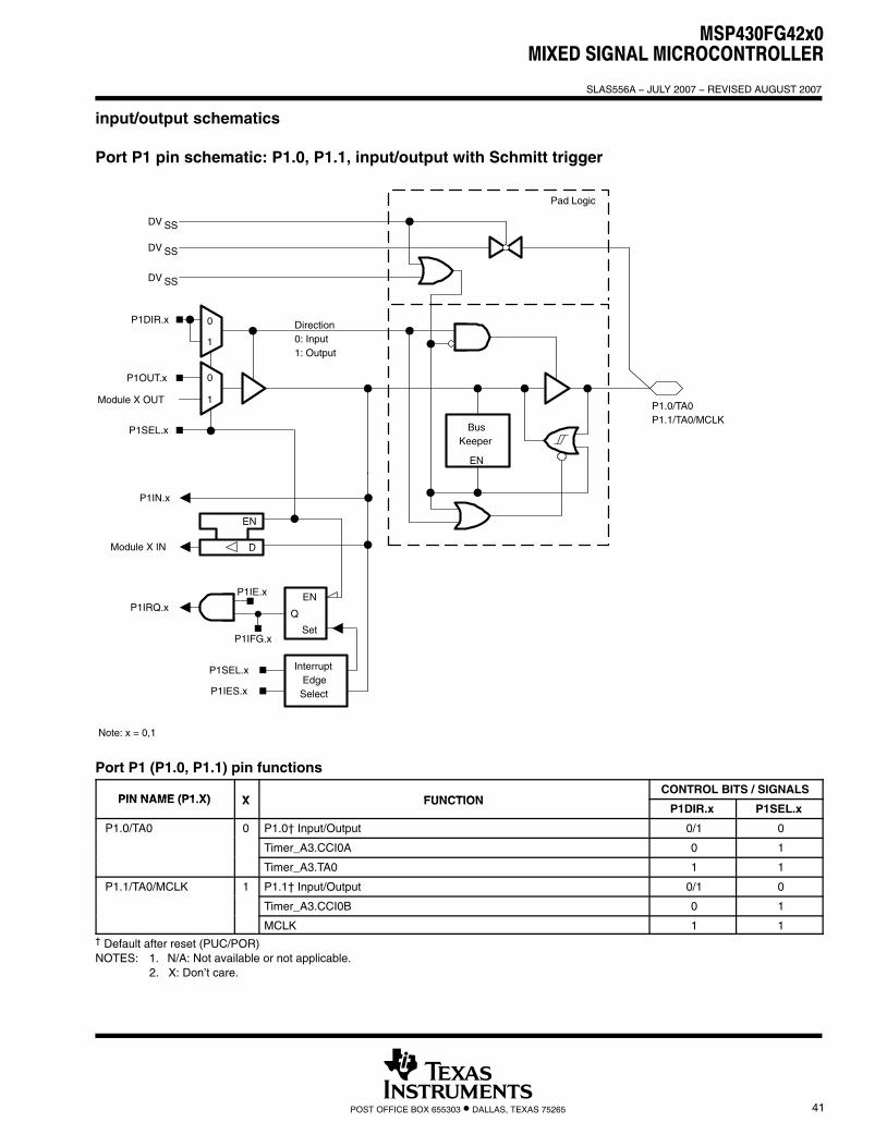
MSP430FG42x0MIXED SIGNAL MICROCONTROLLER
SLAS556A − JULY 2007 − REVISED AUGUST 2007
41POST OFFICE BOX 655303 • DALLAS, TEXAS 75265
input/output schematics
Port P1 pin schematic: P1.0, P1.1, input/output with Schmitt trigger
BusKeeper
EN
Direction0: Input1: Output
P1SEL.x
1
0P1DIR.x
P1IN.x
DV SS
DV SS
Pad Logic
DV SS
P1IRQ.x
D
EN
Module X IN
1
0
Module X OUT
P1OUT.x
Note: x = 0,1
P1.0/TA0P1.1/TA0/MCLK
InterruptEdgeSelect
Q
EN
Set
P1SEL.x
P1IES.x
P1IFG.x
P1IE.x
Port P1 (P1.0, P1.1) pin functions
PIN NAME (P1 X) X FUNCTIONCONTROL BITS / SIGNALS
PIN NAME (P1.X) X FUNCTIONP1DIR.x P1SEL.x
P1.0/TA0 0 P1.0† Input/Output 0/1 0
Timer_A3.CCI0A 0 1
Timer_A3.TA0 1 1
P1.1/TA0/MCLK 1 P1.1† Input/Output 0/1 0
Timer_A3.CCI0B 0 1
MCLK 1 1† Default after reset (PUC/POR)NOTES: 1. N/A: Not available or not applicable.
2. X: Don’t care.
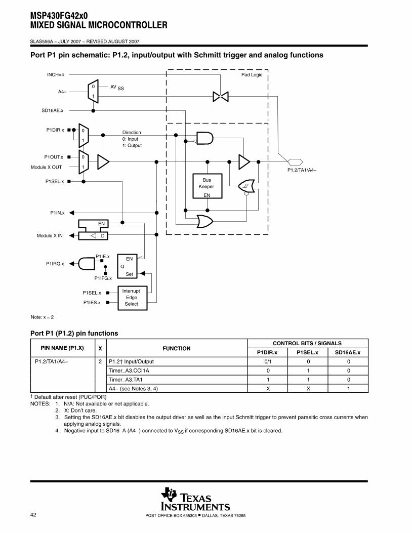
MSP430FG42x0MIXED SIGNAL MICROCONTROLLER
SLAS556A − JULY 2007 − REVISED AUGUST 2007
42 POST OFFICE BOX 655303 • DALLAS, TEXAS 75265
Port P1 pin schematic: P1.2, input/output with Schmitt trigger and analog functions
BusKeeper
EN
Direction0: Input1: Output
P1SEL.x
1
0P1DIR.x
P1IN.x
INCH=4
A4−
Pad Logic
SD16AE.x
P1IRQ.x
D
EN
Module X IN
1
0
Module X OUT
P1OUT.x
Note: x = 2
P1.2/TA1/A4−
1
0 AV SS
InterruptEdgeSelect
Q
EN
Set
P1SEL.x
P1IES.x
P1IFG.x
P1IE.x
Port P1 (P1.2) pin functions
PIN NAME (P1 X) X FUNCTIONCONTROL BITS / SIGNALS
PIN NAME (P1.X) X FUNCTIONP1DIR.x P1SEL.x SD16AE.x
P1.2/TA1/A4− 2 P1.2† Input/Output 0/1 0 0
Timer_A3.CCI1A 0 1 0
Timer_A3.TA1 1 1 0
A4− (see Notes 3, 4) X X 1† Default after reset (PUC/POR)NOTES: 1. N/A: Not available or not applicable.
2. X: Don’t care.3. Setting the SD16AE.x bit disables the output driver as well as the input Schmitt trigger to prevent parasitic cross currents when
applying analog signals.4. Negative input to SD16_A (A4−) connected to VSS if corresponding SD16AE.x bit is cleared.
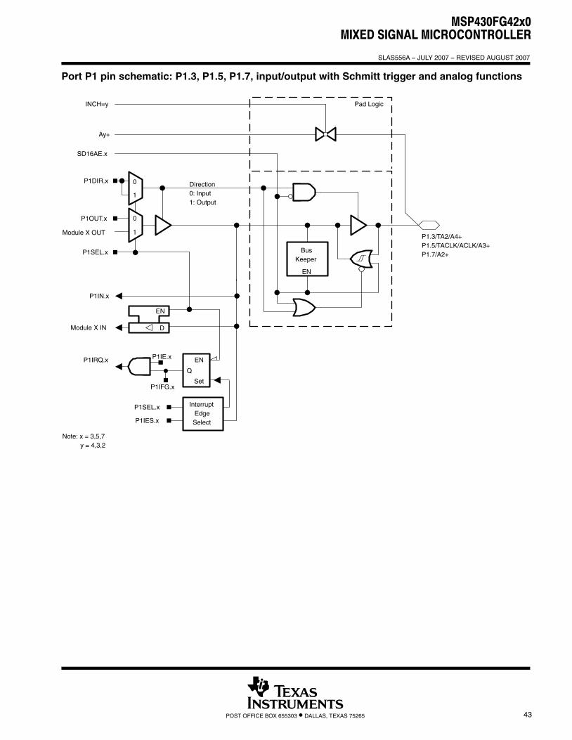
MSP430FG42x0MIXED SIGNAL MICROCONTROLLER
SLAS556A − JULY 2007 − REVISED AUGUST 2007
43POST OFFICE BOX 655303 • DALLAS, TEXAS 75265
Port P1 pin schematic: P1.3, P1.5, P1.7, input/output with Schmitt trigger and analog functions
BusKeeper
EN
Direction0: Input1: Output
P1SEL.x
1
0P1DIR.x
P1IN.x
INCH=y
Ay+
Pad Logic
SD16AE.x
P1IRQ.x
D
EN
Module X IN
1
0
Module X OUT
P1OUT.x
Note: x = 3,5,7 y = 4,3,2
P1.3/TA2/A4+P1.5/TACLK/ACLK/A3+P1.7/A2+
InterruptEdgeSelect
Q
EN
Set
P1SEL.x
P1IES.x
P1IFG.x
P1IE.x
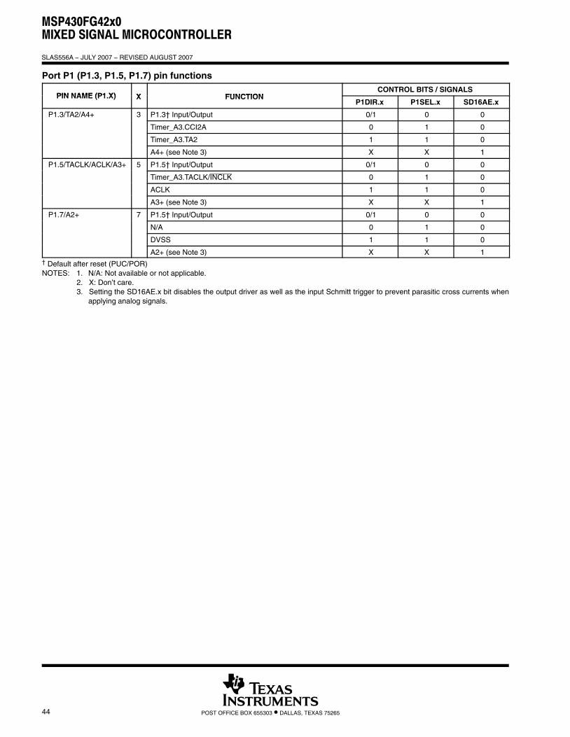
MSP430FG42x0MIXED SIGNAL MICROCONTROLLER
SLAS556A − JULY 2007 − REVISED AUGUST 2007
44 POST OFFICE BOX 655303 • DALLAS, TEXAS 75265
Port P1 (P1.3, P1.5, P1.7) pin functions
PIN NAME (P1 X) X FUNCTIONCONTROL BITS / SIGNALS
PIN NAME (P1.X) X FUNCTIONP1DIR.x P1SEL.x SD16AE.x
P1.3/TA2/A4+ 3 P1.3† Input/Output 0/1 0 0
Timer_A3.CCI2A 0 1 0
Timer_A3.TA2 1 1 0
A4+ (see Note 3) X X 1
P1.5/TACLK/ACLK/A3+ 5 P1.5† Input/Output 0/1 0 0
Timer_A3.TACLK/INCLK 0 1 0
ACLK 1 1 0
A3+ (see Note 3) X X 1
P1.7/A2+ 7 P1.5† Input/Output 0/1 0 0
N/A 0 1 0
DVSS 1 1 0
A2+ (see Note 3) X X 1† Default after reset (PUC/POR)NOTES: 1. N/A: Not available or not applicable.
2. X: Don’t care.3. Setting the SD16AE.x bit disables the output driver as well as the input Schmitt trigger to prevent parasitic cross currents when
applying analog signals.
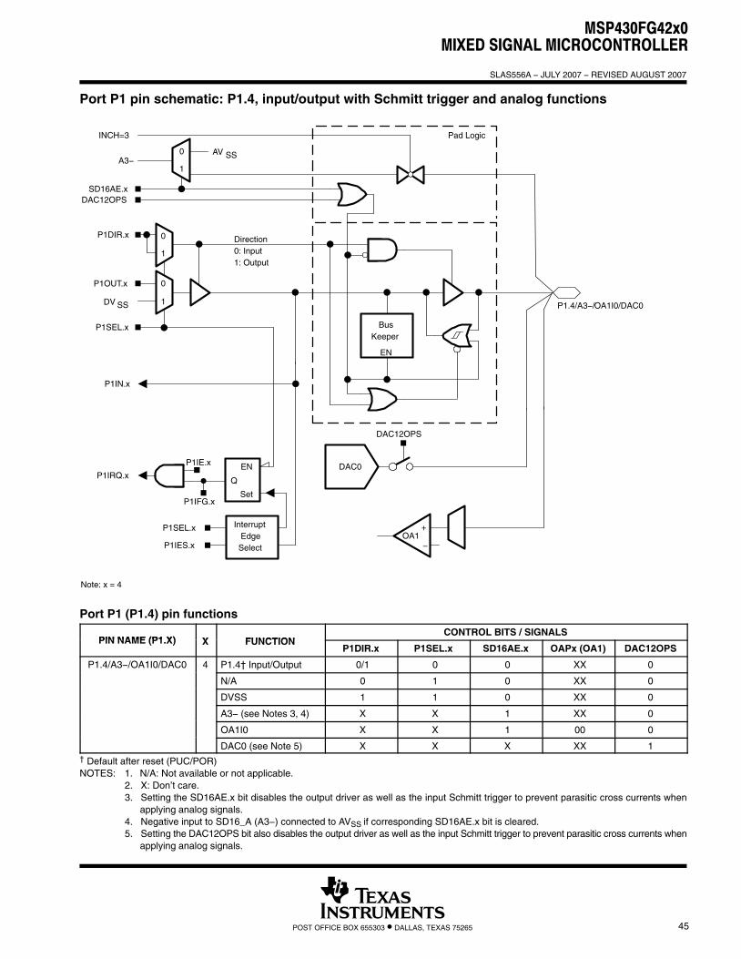
MSP430FG42x0MIXED SIGNAL MICROCONTROLLER
SLAS556A − JULY 2007 − REVISED AUGUST 2007
45POST OFFICE BOX 655303 • DALLAS, TEXAS 75265
Port P1 pin schematic: P1.4, input/output with Schmitt trigger and analog functions
BusKeeper
EN
Direction0: Input1: Output
P1SEL.x
1
0P1DIR.x
P1IN.x
INCH=3
A3−
Pad Logic
SD16AE.x
InterruptEdgeSelect
Q
EN
Set
P1SEL.x
P1IES.x
P1IFG.x
P1IE.x
P1IRQ.x
1
0P1OUT.x
Note: x = 4
P1.4/A3−/OA1I0/DAC0
1
0 AV SS
DAC12OPS
DAC12OPS
DAC0
OA1−
+
DV SS
Port P1 (P1.4) pin functions
PIN NAME (P1 X) X FUNCTIONCONTROL BITS / SIGNALS
PIN NAME (P1.X) X FUNCTIONP1DIR.x P1SEL.x SD16AE.x OAPx (OA1) DAC12OPS
P1.4/A3−/OA1I0/DAC0 4 P1.4† Input/Output 0/1 0 0 XX 0
N/A 0 1 0 XX 0
DVSS 1 1 0 XX 0
A3− (see Notes 3, 4) X X 1 XX 0
OA1I0 X X 1 00 0
DAC0 (see Note 5) X X X XX 1† Default after reset (PUC/POR)NOTES: 1. N/A: Not available or not applicable.
2. X: Don’t care.3. Setting the SD16AE.x bit disables the output driver as well as the input Schmitt trigger to prevent parasitic cross currents when
applying analog signals.4. Negative input to SD16_A (A3−) connected to AVSS if corresponding SD16AE.x bit is cleared.5. Setting the DAC12OPS bit also disables the output driver as well as the input Schmitt trigger to prevent parasitic cross currents when
applying analog signals.
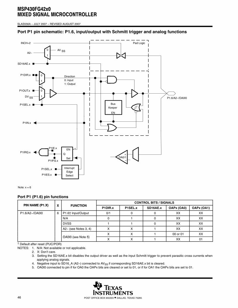
MSP430FG42x0MIXED SIGNAL MICROCONTROLLER
SLAS556A − JULY 2007 − REVISED AUGUST 2007
46 POST OFFICE BOX 655303 • DALLAS, TEXAS 75265
Port P1 pin schematic: P1.6, input/output with Schmitt trigger and analog functions
BusKeeper
EN
Direction0: Input1: Output
P1SEL.x
1
0P1DIR.x
P1IN.x
INCH=2
A2−
Pad Logic
SD16AE.x
InterruptEdgeSelect
Q
EN
Set
P1SEL.x
P1IES.x
P1IFG.x
P1IE.x
P1IRQ.x
1
0P1OUT.x
Note: x = 6
P1.6/A2−/OA0I0
1
0 AV SS
−
+OA0/1
DV SS
Port P1 (P1.6) pin functions
PIN NAME (P1 X) X FUNCTIONCONTROL BITS / SIGNALS
PIN NAME (P1.X) X FUNCTIONP1DIR.x P1SEL.x SD16AE.x OAPx (OA0) OAPx (OA1)
P1.6/A2−/OA0I0 6 P1.6† Input/Output 0/1 0 0 XX XX
N/A 0 1 0 XX XX
DVSS 1 1 0 XX XX
A2− (see Notes 3, 4) X X 1 XX XX
OA0I0 (see Note 5)X X 1 00 or 01 XX
OA0I0 (see Note 5)X X 1 XX 01
† Default after reset (PUC/POR)NOTES: 1. N/A: Not available or not applicable.
2. X: Don’t care.3. Setting the SD16AE.x bit disables the output driver as well as the input Schmitt trigger to prevent parasitic cross currents when
applying analog signals.4. Negative input to SD16_A (A2−) connected to AVSS if corresponding SD16AE.x bit is cleared.5. OA0I0 connected to pin if for OA0 the OAPx bits are cleared or set to 01, or if for OA1 the OAPx bits are set to 01.
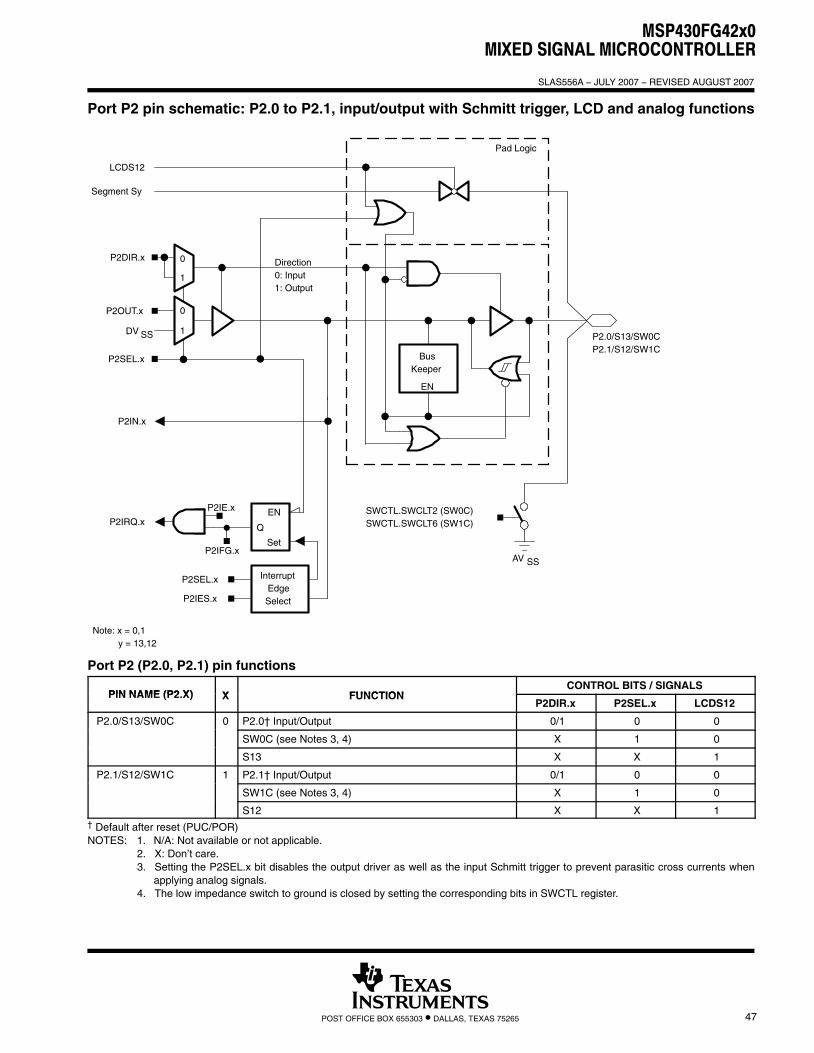
MSP430FG42x0MIXED SIGNAL MICROCONTROLLER
SLAS556A − JULY 2007 − REVISED AUGUST 2007
47POST OFFICE BOX 655303 • DALLAS, TEXAS 75265
Port P2 pin schematic: P2.0 to P2.1, input/output with Schmitt trigger, LCD and analog functions
BusKeeper
EN
Direction0: Input1: Output
P2SEL.x
1
0P2DIR.x
P2IN.x
LCDS12
Segment Sy
Pad Logic
P2IRQ.x
1
0P2OUT.x
Note: x = 0,1 y = 13,12
P2.0/S13/SW0CP2.1/S12/SW1C
InterruptEdgeSelect
Q
EN
Set
P2SEL.x
P2IES.x
P2IFG.x
P2IE.x SWCTL.SWCLT2 (SW0C)SWCTL.SWCLT6 (SW1C)
AV SS
DV SS
Port P2 (P2.0, P2.1) pin functions
PIN NAME (P2 X) X FUNCTIONCONTROL BITS / SIGNALS
PIN NAME (P2.X) X FUNCTIONP2DIR.x P2SEL.x LCDS12
P2.0/S13/SW0C 0 P2.0† Input/Output 0/1 0 0
SW0C (see Notes 3, 4) X 1 0
S13 X X 1
P2.1/S12/SW1C 1 P2.1† Input/Output 0/1 0 0
SW1C (see Notes 3, 4) X 1 0
S12 X X 1† Default after reset (PUC/POR)NOTES: 1. N/A: Not available or not applicable.
2. X: Don’t care.3. Setting the P2SEL.x bit disables the output driver as well as the input Schmitt trigger to prevent parasitic cross currents when
applying analog signals.4. The low impedance switch to ground is closed by setting the corresponding bits in SWCTL register.
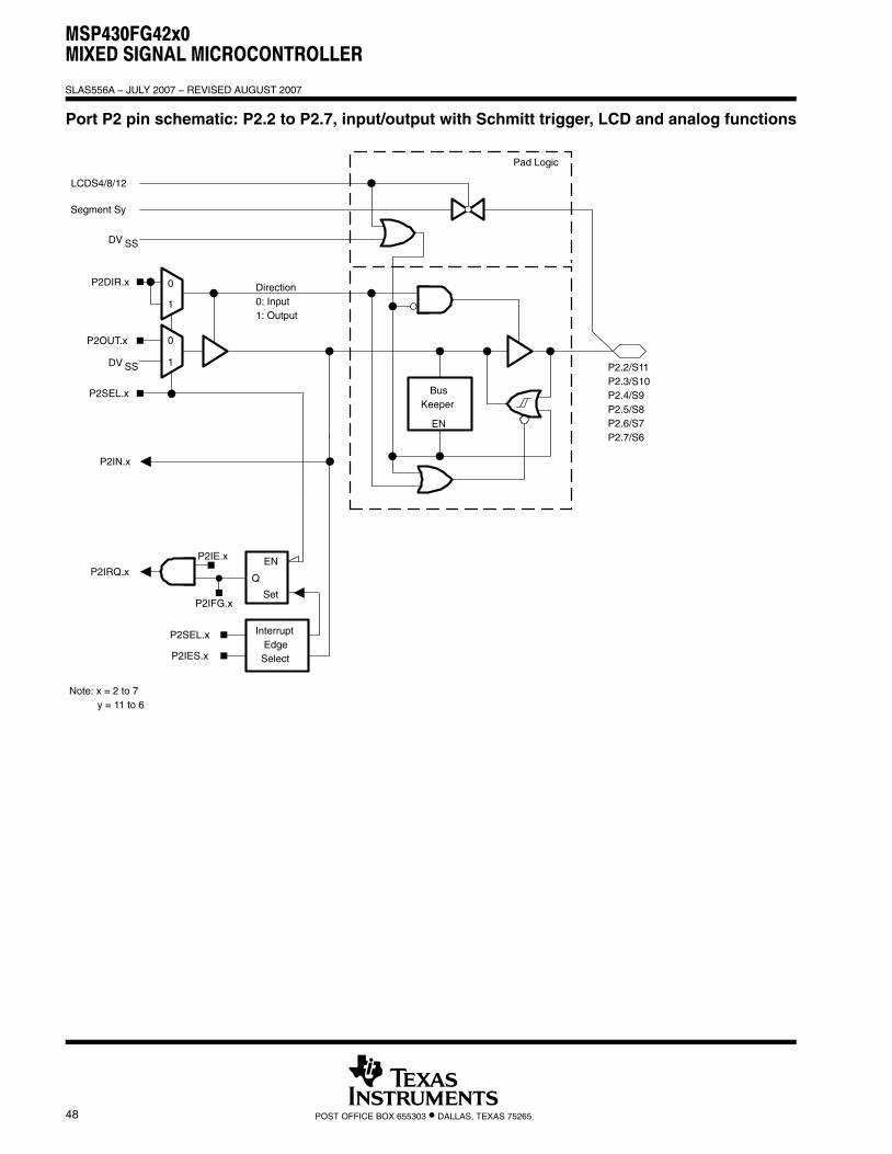
MSP430FG42x0MIXED SIGNAL MICROCONTROLLER
SLAS556A − JULY 2007 − REVISED AUGUST 2007
48 POST OFFICE BOX 655303 • DALLAS, TEXAS 75265
Port P2 pin schematic: P2.2 to P2.7, input/output with Schmitt trigger, LCD and analog functions
BusKeeper
EN
Direction0: Input1: Output
P2SEL.x
1
0P2DIR.x
P2IN.x
LCDS4/8/12
Segment Sy
Pad Logic
DV SS
P2IRQ.x
1
0P2OUT.x
Note: x = 2 to 7 y = 11 to 6
P2.2/S11P2.3/S10P2.4/S9P2.5/S8P2.6/S7P2.7/S6
InterruptEdgeSelect
Q
EN
Set
P2SEL.x
P2IES.x
P2IFG.x
P2IE.x
DV SS
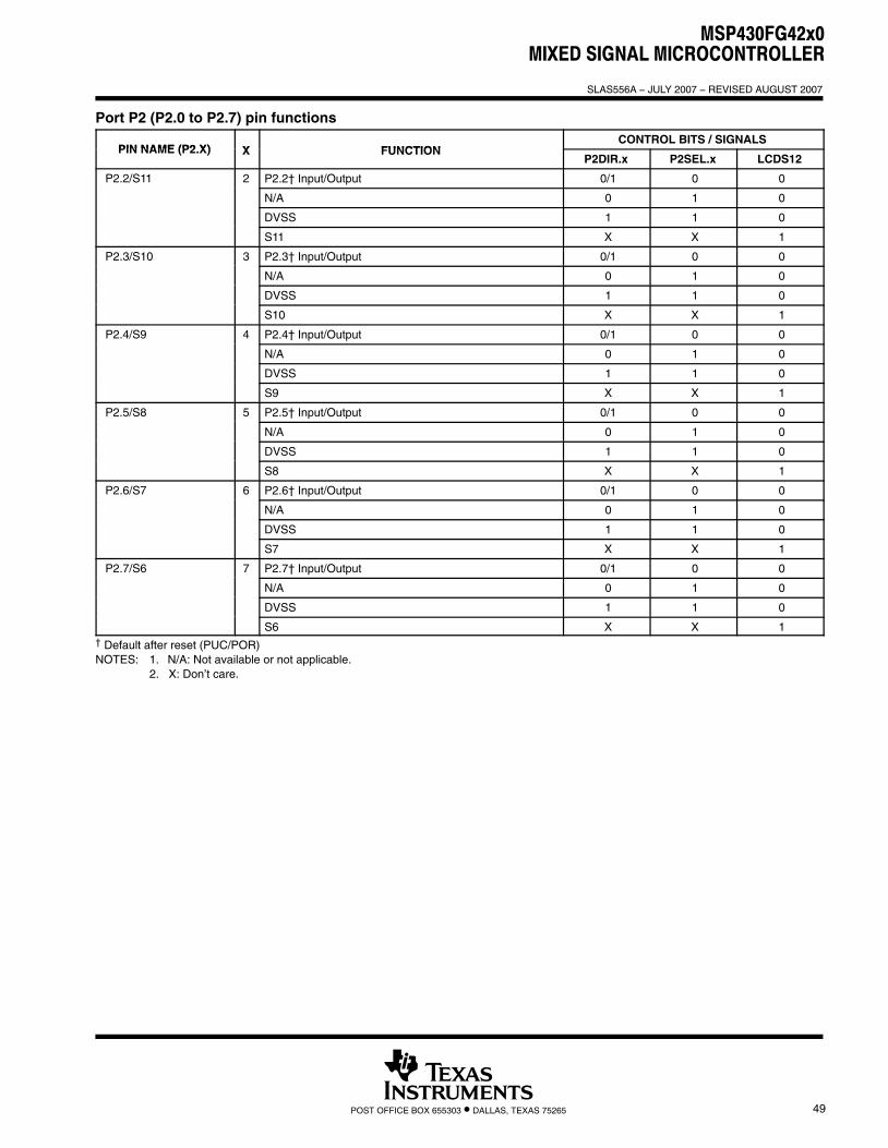
MSP430FG42x0MIXED SIGNAL MICROCONTROLLER
SLAS556A − JULY 2007 − REVISED AUGUST 2007
49POST OFFICE BOX 655303 • DALLAS, TEXAS 75265
Port P2 (P2.0 to P2.7) pin functions
PIN NAME (P2 X) X FUNCTIONCONTROL BITS / SIGNALS
PIN NAME (P2.X) X FUNCTIONP2DIR.x P2SEL.x LCDS12
P2.2/S11 2 P2.2† Input/Output 0/1 0 0
N/A 0 1 0
DVSS 1 1 0
S11 X X 1
P2.3/S10 3 P2.3† Input/Output 0/1 0 0
N/A 0 1 0
DVSS 1 1 0
S10 X X 1
P2.4/S9 4 P2.4† Input/Output 0/1 0 0
N/A 0 1 0
DVSS 1 1 0
S9 X X 1
P2.5/S8 5 P2.5† Input/Output 0/1 0 0
N/A 0 1 0
DVSS 1 1 0
S8 X X 1
P2.6/S7 6 P2.6† Input/Output 0/1 0 0
N/A 0 1 0
DVSS 1 1 0
S7 X X 1
P2.7/S6 7 P2.7† Input/Output 0/1 0 0
N/A 0 1 0
DVSS 1 1 0
S6 X X 1† Default after reset (PUC/POR)NOTES: 1. N/A: Not available or not applicable.
2. X: Don’t care.
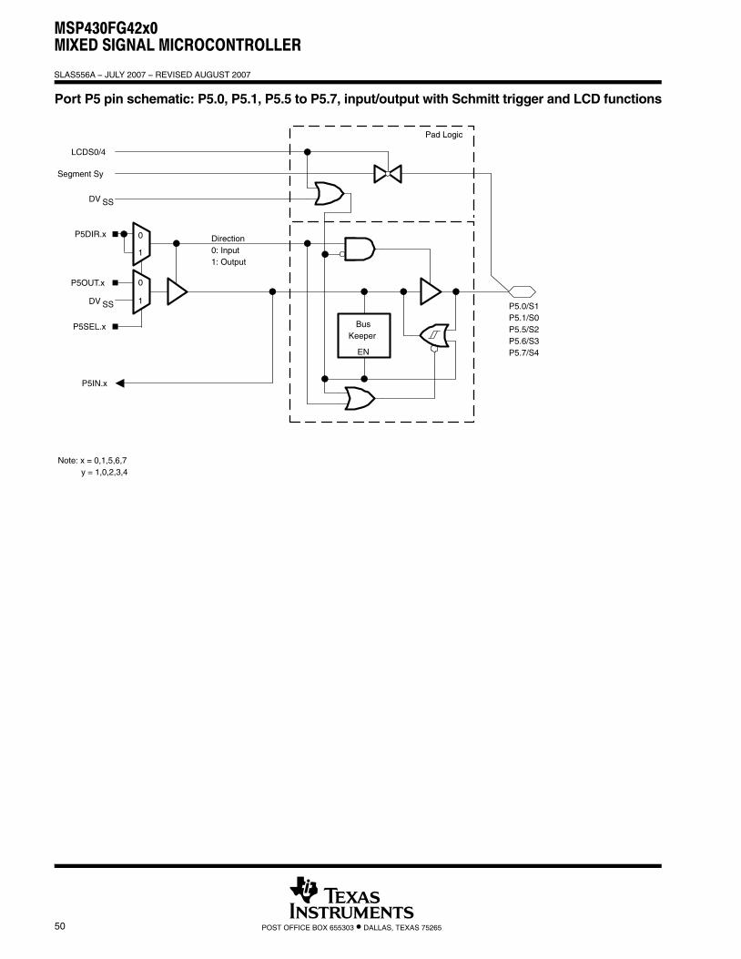
MSP430FG42x0MIXED SIGNAL MICROCONTROLLER
SLAS556A − JULY 2007 − REVISED AUGUST 2007
50 POST OFFICE BOX 655303 • DALLAS, TEXAS 75265
Port P5 pin schematic: P5.0, P5.1, P5.5 to P5.7, input/output with Schmitt trigger and LCD functions
BusKeeper
EN
Direction0: Input1: Output
P5SEL.x
1
0P5DIR.x
P5IN.x
LCDS0/4
Segment Sy
Pad Logic
DV SS
1
0P5OUT.x
Note: x = 0,1,5,6,7 y = 1,0,2,3,4
P5.0/S1P5.1/S0P5.5/S2P5.6/S3P5.7/S4
DV SS
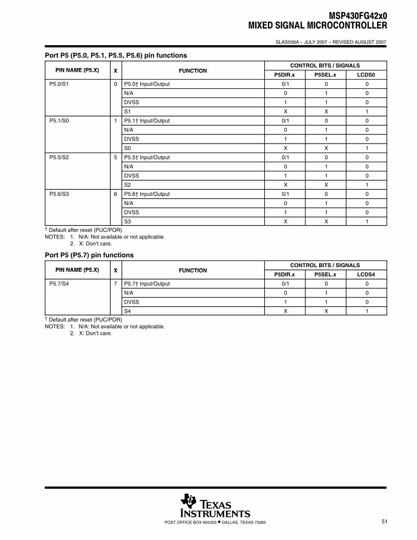
MSP430FG42x0MIXED SIGNAL MICROCONTROLLER
SLAS556A − JULY 2007 − REVISED AUGUST 2007
51POST OFFICE BOX 655303 • DALLAS, TEXAS 75265
Port P5 (P5.0, P5.1, P5.5, P5.6) pin functions
PIN NAME (P5 X) X FUNCTIONCONTROL BITS / SIGNALS
PIN NAME (P5.X) X FUNCTIONP5DIR.x P5SEL.x LCDS0
P5.0/S1 0 P5.0† Input/Output 0/1 0 0
N/A 0 1 0
DVSS 1 1 0
S1 X X 1
P5.1/S0 1 P5.1† Input/Output 0/1 0 0
N/A 0 1 0
DVSS 1 1 0
S0 X X 1
P5.5/S2 5 P5.5† Input/Output 0/1 0 0
N/A 0 1 0
DVSS 1 1 0
S2 X X 1
P5.6/S3 6 P5.6† Input/Output 0/1 0 0
N/A 0 1 0
DVSS 1 1 0
S3 X X 1† Default after reset (PUC/POR)NOTES: 1. N/A: Not available or not applicable.
2. X: Don’t care.
Port P5 (P5.7) pin functions
PIN NAME (P5 X) X FUNCTIONCONTROL BITS / SIGNALS
PIN NAME (P5.X) X FUNCTIONP5DIR.x P5SEL.x LCDS4
P5.7/S4 7 P5.7† Input/Output 0/1 0 0
N/A 0 1 0
DVSS 1 1 0
S4 X X 1† Default after reset (PUC/POR)NOTES: 1. N/A: Not available or not applicable.
2. X: Don’t care.
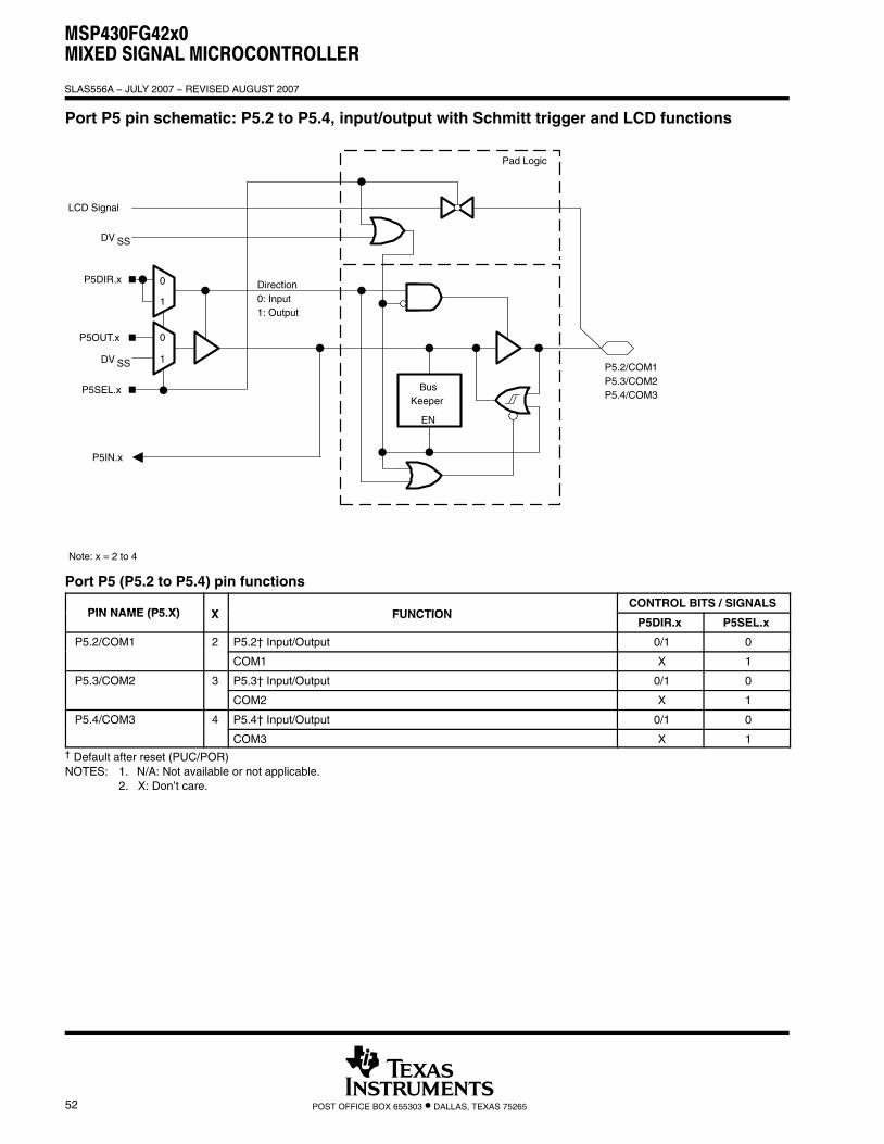
MSP430FG42x0MIXED SIGNAL MICROCONTROLLER
SLAS556A − JULY 2007 − REVISED AUGUST 2007
52 POST OFFICE BOX 655303 • DALLAS, TEXAS 75265
Port P5 pin schematic: P5.2 to P5.4, input/output with Schmitt trigger and LCD functions
BusKeeper
EN
Direction0: Input1: Output
P5SEL.x
1
0P5DIR.x
P5IN.x
LCD Signal
Pad Logic
DV SS
1
0P5OUT.x
Note: x = 2 to 4
P5.2/COM1P5.3/COM2P5.4/COM3
DV SS
Port P5 (P5.2 to P5.4) pin functions
PIN NAME (P5 X) X FUNCTIONCONTROL BITS / SIGNALS
PIN NAME (P5.X) X FUNCTIONP5DIR.x P5SEL.x
P5.2/COM1 2 P5.2† Input/Output 0/1 0
COM1 X 1
P5.3/COM2 3 P5.3† Input/Output 0/1 0
COM2 X 1
P5.4/COM3 4 P5.4† Input/Output 0/1 0
COM3 X 1† Default after reset (PUC/POR)NOTES: 1. N/A: Not available or not applicable.
2. X: Don’t care.
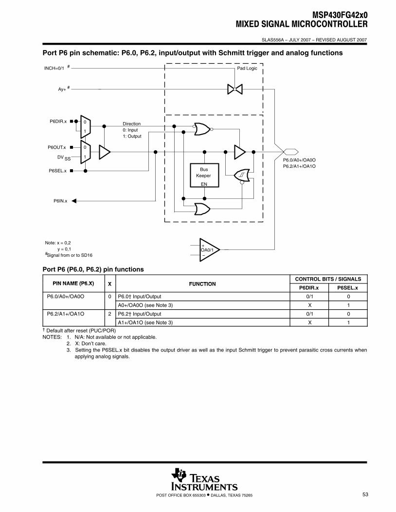
MSP430FG42x0MIXED SIGNAL MICROCONTROLLER
SLAS556A − JULY 2007 − REVISED AUGUST 2007
53POST OFFICE BOX 655303 • DALLAS, TEXAS 75265
Port P6 pin schematic: P6.0, P6.2, input/output with Schmitt trigger and analog functions
BusKeeper
EN
Direction0: Input1: Output
P6SEL.x
1
0P6DIR.x
P6IN.x
INCH=0/1 #
Ay+ #
Pad Logic
1
0
DV SS
P6OUT.x
Note: x = 0,2 y = 0,1#Signal from or to SD16
P6.0/A0+/OA0OP6.2/A1+/OA1O
−
+OA0/1
Port P6 (P6.0, P6.2) pin functions
PIN NAME (P6 X) X FUNCTIONCONTROL BITS / SIGNALS
PIN NAME (P6.X) X FUNCTIONP6DIR.x P6SEL.x
P6.0/A0+/OA0O 0 P6.0† Input/Output 0/1 0
A0+/OA0O (see Note 3) X 1
P6.2/A1+/OA1O 2 P6.2† Input/Output 0/1 0
A1+/OA1O (see Note 3) X 1† Default after reset (PUC/POR)NOTES: 1. N/A: Not available or not applicable.
2. X: Don’t care.3. Setting the P6SEL.x bit disables the output driver as well as the input Schmitt trigger to prevent parasitic cross currents when
applying analog signals.
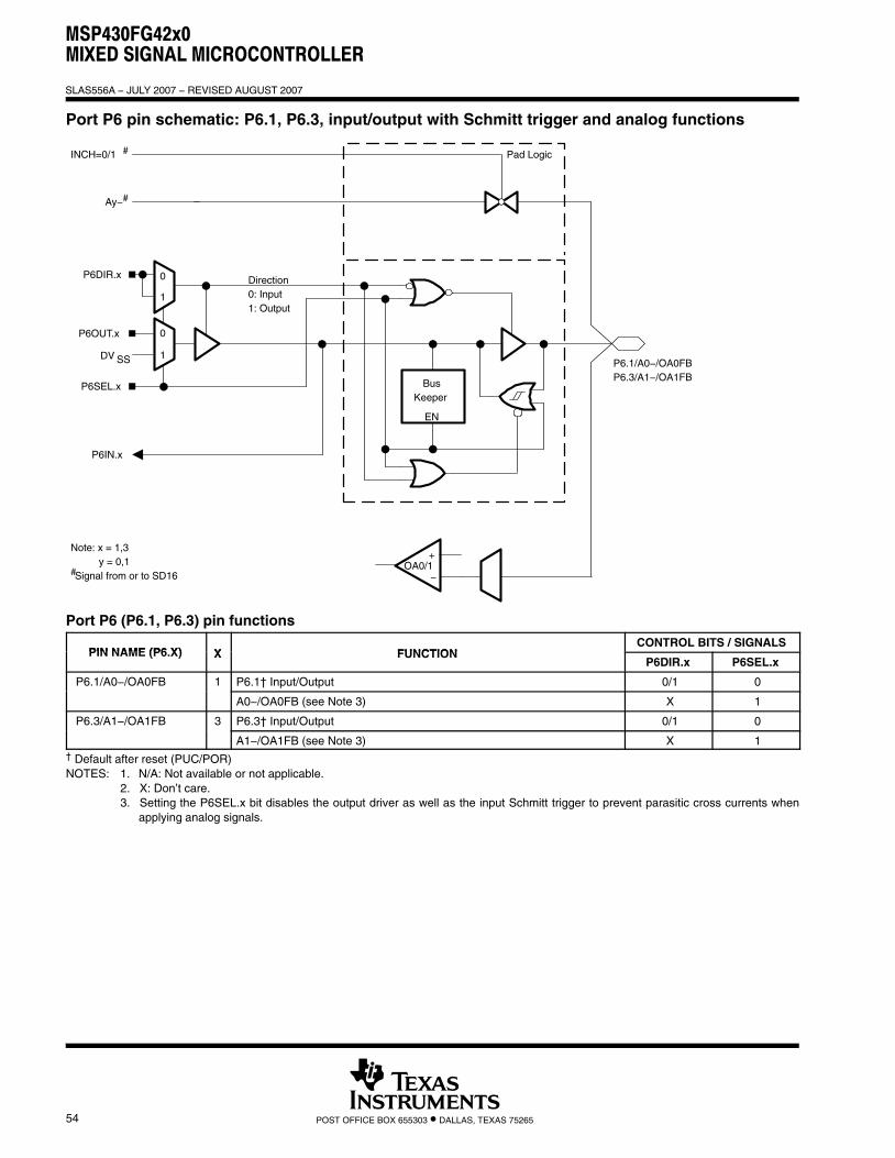
MSP430FG42x0MIXED SIGNAL MICROCONTROLLER
SLAS556A − JULY 2007 − REVISED AUGUST 2007
54 POST OFFICE BOX 655303 • DALLAS, TEXAS 75265
Port P6 pin schematic: P6.1, P6.3, input/output with Schmitt trigger and analog functions
BusKeeper
EN
Direction0: Input1: Output
P6SEL.x
1
0P6DIR.x
P6IN.x
INCH=0/1 #
Ay−#
Pad Logic
1
0
DV SS
P6OUT.x
Note: x = 1,3 y = 0,1#Signal from or to SD16
P6.1/A0−/OA0FBP6.3/A1−/OA1FB
−
+OA0/1
Port P6 (P6.1, P6.3) pin functions
PIN NAME (P6 X) X FUNCTIONCONTROL BITS / SIGNALS
PIN NAME (P6.X) X FUNCTIONP6DIR.x P6SEL.x
P6.1/A0−/OA0FB 1 P6.1† Input/Output 0/1 0
A0−/OA0FB (see Note 3) X 1
P6.3/A1−/OA1FB 3 P6.3† Input/Output 0/1 0
A1−/OA1FB (see Note 3) X 1† Default after reset (PUC/POR)NOTES: 1. N/A: Not available or not applicable.
2. X: Don’t care.3. Setting the P6SEL.x bit disables the output driver as well as the input Schmitt trigger to prevent parasitic cross currents when
applying analog signals.
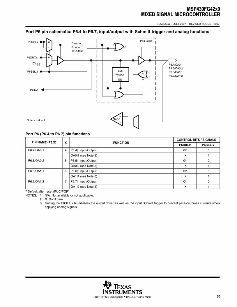
MSP430FG42x0MIXED SIGNAL MICROCONTROLLER
SLAS556A − JULY 2007 − REVISED AUGUST 2007
55POST OFFICE BOX 655303 • DALLAS, TEXAS 75265
Port P6 pin schematic: P6.4 to P6.7, input/output with Schmitt trigger and analog functions
BusKeeper
EN
Direction0: Input1: Output
P6SEL.x
1
0P6DIR.x
P6IN.x
1
0
DV SS
P6OUT.x
Note: x = 4 to 7
P6.4/OA0I1P6.5/OA0I2P6.6/OA1I1P6.7/OA1I2
−
+OA0/1
Pad Logic
Port P6 (P6.4 to P6.7) pin functions
PIN NAME (P6 X) X FUNCTIONCONTROL BITS / SIGNALS
PIN NAME (P6.X) X FUNCTIONP6DIR.x P6SEL.x
P6.4/OA0I1 4 P6.4† Input/Output 0/1 0
OA0I1 (see Note 3) X 1
P6.5/OA0I2 5 P6.5† Input/Output 0/1 0
OA0I2 (see Note 3) X 1
P6.6/OA1I1 6 P6.6† Input/Output 0/1 0
OA1I1 (see Note 3) X 1
P6.7/OA1I2 7 P6.7† Input/Output 0/1 0
OA1I2 (see Note 3) X 1† Default after reset (PUC/POR)NOTES: 1. N/A: Not available or not applicable.
2. X: Don’t care.3. Setting the P6SEL.x bit disables the output driver as well as the input Schmitt trigger to prevent parasitic cross currents when
applying analog signals.
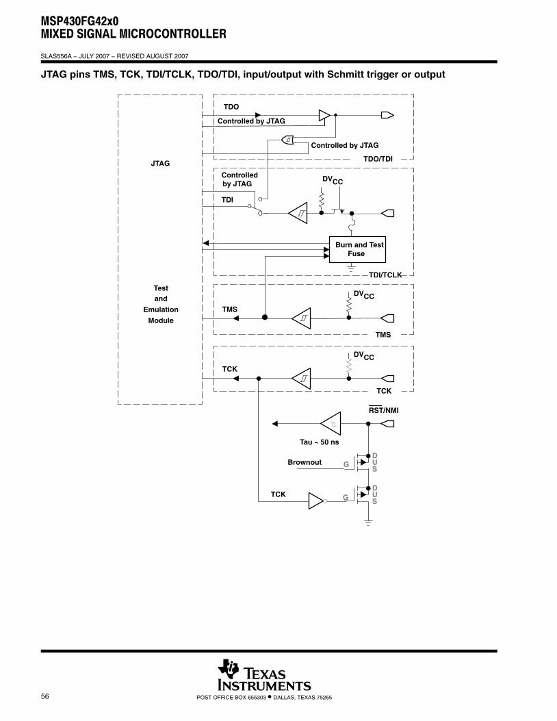
MSP430FG42x0MIXED SIGNAL MICROCONTROLLER
SLAS556A − JULY 2007 − REVISED AUGUST 2007
56 POST OFFICE BOX 655303 • DALLAS, TEXAS 75265
JTAG pins TMS, TCK, TDI/TCLK, TDO/TDI, input/output with Schmitt trigger or output
TDI
TDO
TMS
TDI/TCLK
TDO/TDI
Controlledby JTAG
TCK
TMS
TCK
DVCC
Controlled by JTAG
Test
JTAG
and
Emulation
Module
DVCC
DVCC
Burn and TestFuse
RST/NMI
GD
SU
GD
SUTCK
Tau ~ 50 ns
Brownout
Controlled by JTAG
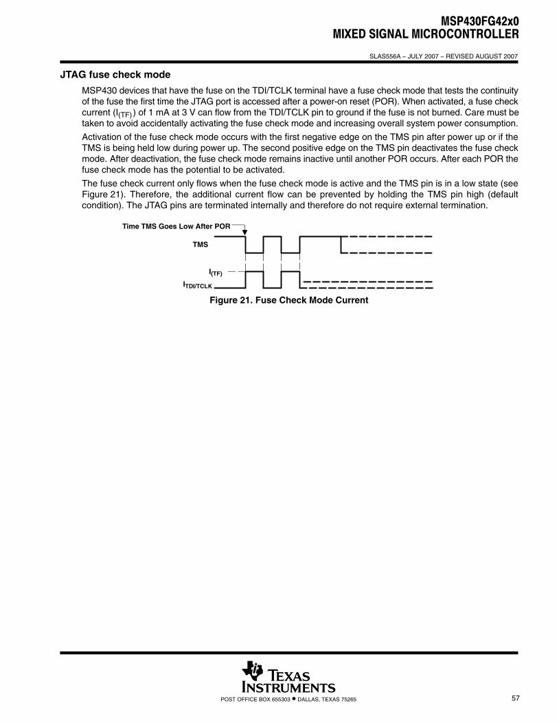
MSP430FG42x0MIXED SIGNAL MICROCONTROLLER
SLAS556A − JULY 2007 − REVISED AUGUST 2007
57POST OFFICE BOX 655303 • DALLAS, TEXAS 75265
JTAG fuse check mode
MSP430 devices that have the fuse on the TDI/TCLK terminal have a fuse check mode that tests the continuityof the fuse the first time the JTAG port is accessed after a power-on reset (POR). When activated, a fuse checkcurrent (I(TF)) of 1 mA at 3 V can flow from the TDI/TCLK pin to ground if the fuse is not burned. Care must betaken to avoid accidentally activating the fuse check mode and increasing overall system power consumption.
Activation of the fuse check mode occurs with the first negative edge on the TMS pin after power up or if theTMS is being held low during power up. The second positive edge on the TMS pin deactivates the fuse checkmode. After deactivation, the fuse check mode remains inactive until another POR occurs. After each POR thefuse check mode has the potential to be activated.
The fuse check current only flows when the fuse check mode is active and the TMS pin is in a low state (seeFigure 21). Therefore, the additional current flow can be prevented by holding the TMS pin high (defaultcondition). The JTAG pins are terminated internally and therefore do not require external termination.
Time TMS Goes Low After POR
TMS
I(TF)
ITDI/TCLK
Figure 21. Fuse Check Mode Current
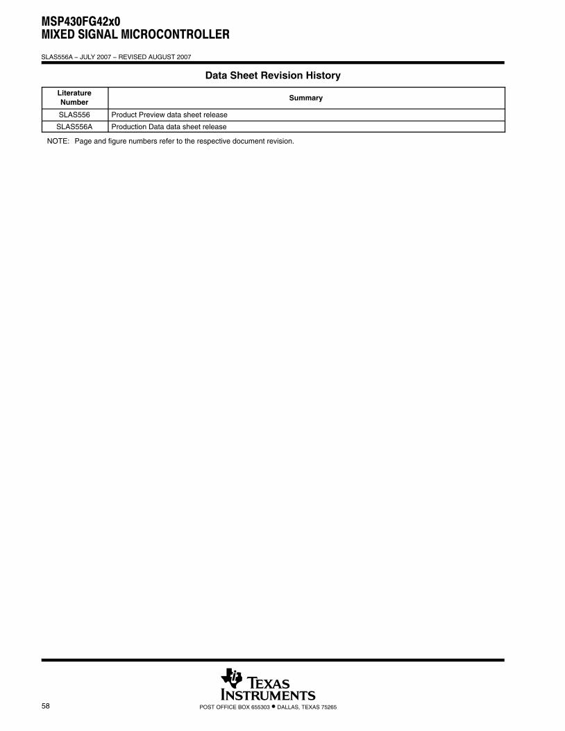
MSP430FG42x0MIXED SIGNAL MICROCONTROLLER
SLAS556A − JULY 2007 − REVISED AUGUST 2007
58 POST OFFICE BOX 655303 • DALLAS, TEXAS 75265
Data Sheet Revision History
LiteratureNumber Summary
SLAS556 Product Preview data sheet release
SLAS556A Production Data data sheet release
NOTE: Page and figure numbers refer to the respective document revision.
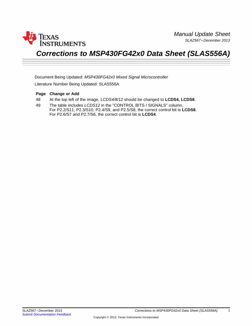
Manual Update SheetSLAZ567–December 2013
Corrections to MSP430FG42x0 Data Sheet (SLAS556A)
Document Being Updated: MSP430FG42x0 Mixed Signal Microcontroller
Literature Number Being Updated: SLAS556A
Page Change or Add48 At the top left of the image, LCDS4/8/12 should be changed to LCDS4, LCDS8.49 The table includes LCDS12 in the "CONTROL BITS / SIGNALS" column.
For P2.2/S11, P2.3/S10, P2.4/S9, and P2.5/S8, the correct control bit is LCDS8.For P2.6/S7 and P2.7/S6, the correct control bit is LCDS4.
1SLAZ567–December 2013 Corrections to MSP430FG42x0 Data Sheet (SLAS556A)Submit Documentation Feedback
Copyright © 2013, Texas Instruments Incorporated

PACKAGE OPTION ADDENDUM
www.ti.com 28-Apr-2015
Addendum-Page 1
PACKAGING INFORMATION
Orderable Device Status(1)
Package Type PackageDrawing
Pins PackageQty
Eco Plan(2)
Lead/Ball Finish(6)
MSL Peak Temp(3)
Op Temp (°C) Device Marking(4/5)
Samples
MSP430FG4250IDL ACTIVE SSOP DL 48 25 Green (RoHS& no Sb/Br)
CU NIPDAU Level-2-260C-1 YEAR -40 to 85 M430FG4250
MSP430FG4250IDLR ACTIVE SSOP DL 48 1000 Green (RoHS& no Sb/Br)
CU NIPDAU Level-2-260C-1 YEAR -40 to 85 M430FG4250
MSP430FG4250IRGZR ACTIVE VQFN RGZ 48 2500 Green (RoHS& no Sb/Br)
CU NIPDAU Level-3-260C-168 HR -40 to 85 M430FG4250
MSP430FG4250IRGZT NRND VQFN RGZ 48 250 Green (RoHS& no Sb/Br)
CU NIPDAU Level-3-260C-168 HR -40 to 85 M430FG4250
MSP430FG4260IDL ACTIVE SSOP DL 48 25 Green (RoHS& no Sb/Br)
CU NIPDAU Level-2-260C-1 YEAR -40 to 85 M430FG4260
MSP430FG4260IDLR ACTIVE SSOP DL 48 1000 Green (RoHS& no Sb/Br)
CU NIPDAU Level-2-260C-1 YEAR -40 to 85 M430FG4260
MSP430FG4260IRGZR ACTIVE VQFN RGZ 48 2500 Green (RoHS& no Sb/Br)
CU NIPDAU Level-3-260C-168 HR -40 to 85 M430FG4260
MSP430FG4270IDL ACTIVE SSOP DL 48 25 Green (RoHS& no Sb/Br)
CU NIPDAU Level-2-260C-1 YEAR -40 to 85 M430FG4270
MSP430FG4270IDLR ACTIVE SSOP DL 48 1000 Green (RoHS& no Sb/Br)
CU NIPDAU Level-2-260C-1 YEAR -40 to 85 M430FG4270
MSP430FG4270IRGZR ACTIVE VQFN RGZ 48 2500 Green (RoHS& no Sb/Br)
CU NIPDAU Level-3-260C-168 HR -40 to 85 M430FG4270
MSP430FG4270IRGZT ACTIVE VQFN RGZ 48 250 Green (RoHS& no Sb/Br)
CU NIPDAU Level-3-260C-168 HR -40 to 85 M430FG4270
(1) The marketing status values are defined as follows:ACTIVE: Product device recommended for new designs.LIFEBUY: TI has announced that the device will be discontinued, and a lifetime-buy period is in effect.NRND: Not recommended for new designs. Device is in production to support existing customers, but TI does not recommend using this part in a new design.PREVIEW: Device has been announced but is not in production. Samples may or may not be available.OBSOLETE: TI has discontinued the production of the device.
(2) Eco Plan - The planned eco-friendly classification: Pb-Free (RoHS), Pb-Free (RoHS Exempt), or Green (RoHS & no Sb/Br) - please check http://www.ti.com/productcontent for the latest availabilityinformation and additional product content details.TBD: The Pb-Free/Green conversion plan has not been defined.Pb-Free (RoHS): TI's terms "Lead-Free" or "Pb-Free" mean semiconductor products that are compatible with the current RoHS requirements for all 6 substances, including the requirement thatlead not exceed 0.1% by weight in homogeneous materials. Where designed to be soldered at high temperatures, TI Pb-Free products are suitable for use in specified lead-free processes.
PACKAGE OPTION ADDENDUM
www.ti.com 28-Apr-2015
Addendum-Page 2
Pb-Free (RoHS Exempt): This component has a RoHS exemption for either 1) lead-based flip-chip solder bumps used between the die and package, or 2) lead-based die adhesive used betweenthe die and leadframe. The component is otherwise considered Pb-Free (RoHS compatible) as defined above.Green (RoHS & no Sb/Br): TI defines "Green" to mean Pb-Free (RoHS compatible), and free of Bromine (Br) and Antimony (Sb) based flame retardants (Br or Sb do not exceed 0.1% by weightin homogeneous material)
(3) MSL, Peak Temp. - The Moisture Sensitivity Level rating according to the JEDEC industry standard classifications, and peak solder temperature.
(4) There may be additional marking, which relates to the logo, the lot trace code information, or the environmental category on the device.
(5) Multiple Device Markings will be inside parentheses. Only one Device Marking contained in parentheses and separated by a "~" will appear on a device. If a line is indented then it is a continuationof the previous line and the two combined represent the entire Device Marking for that device.
(6) Lead/Ball Finish - Orderable Devices may have multiple material finish options. Finish options are separated by a vertical ruled line. Lead/Ball Finish values may wrap to two lines if the finishvalue exceeds the maximum column width.
Important Information and Disclaimer:The information provided on this page represents TI's knowledge and belief as of the date that it is provided. TI bases its knowledge and belief on informationprovided by third parties, and makes no representation or warranty as to the accuracy of such information. Efforts are underway to better integrate information from third parties. TI has taken andcontinues to take reasonable steps to provide representative and accurate information but may not have conducted destructive testing or chemical analysis on incoming materials and chemicals.TI and TI suppliers consider certain information to be proprietary, and thus CAS numbers and other limited information may not be available for release.
In no event shall TI's liability arising out of such information exceed the total purchase price of the TI part(s) at issue in this document sold by TI to Customer on an annual basis.
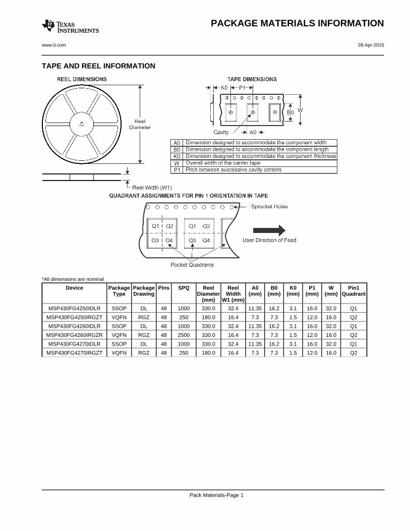
TAPE AND REEL INFORMATION
*All dimensions are nominal
Device PackageType
PackageDrawing
Pins SPQ ReelDiameter
(mm)
ReelWidth
W1 (mm)
A0(mm)
B0(mm)
K0(mm)
P1(mm)
W(mm)
Pin1Quadrant
MSP430FG4250IDLR SSOP DL 48 1000 330.0 32.4 11.35 16.2 3.1 16.0 32.0 Q1
MSP430FG4250IRGZT VQFN RGZ 48 250 180.0 16.4 7.3 7.3 1.5 12.0 16.0 Q2
MSP430FG4260IDLR SSOP DL 48 1000 330.0 32.4 11.35 16.2 3.1 16.0 32.0 Q1
MSP430FG4260IRGZR VQFN RGZ 48 2500 330.0 16.4 7.3 7.3 1.5 12.0 16.0 Q2
MSP430FG4270IDLR SSOP DL 48 1000 330.0 32.4 11.35 16.2 3.1 16.0 32.0 Q1
MSP430FG4270IRGZT VQFN RGZ 48 250 180.0 16.4 7.3 7.3 1.5 12.0 16.0 Q2
PACKAGE MATERIALS INFORMATION
www.ti.com 28-Apr-2015
Pack Materials-Page 1
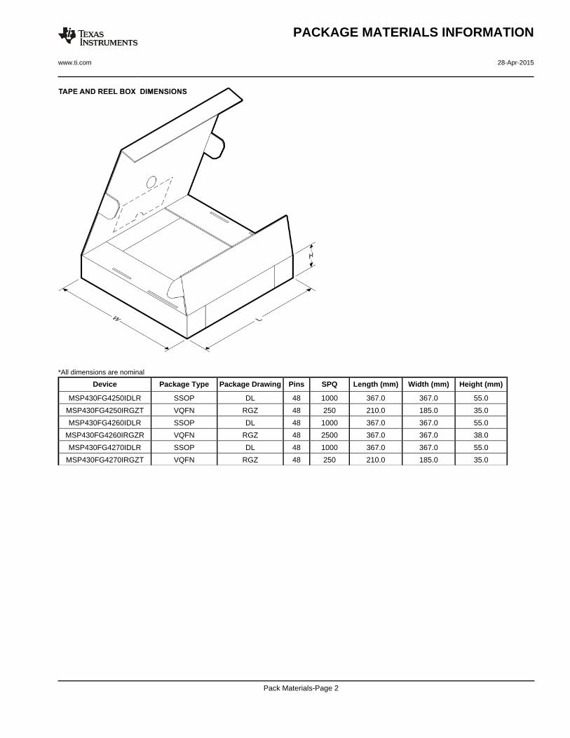
*All dimensions are nominal
Device Package Type Package Drawing Pins SPQ Length (mm) Width (mm) Height (mm)
MSP430FG4250IDLR SSOP DL 48 1000 367.0 367.0 55.0
MSP430FG4250IRGZT VQFN RGZ 48 250 210.0 185.0 35.0
MSP430FG4260IDLR SSOP DL 48 1000 367.0 367.0 55.0
MSP430FG4260IRGZR VQFN RGZ 48 2500 367.0 367.0 38.0
MSP430FG4270IDLR SSOP DL 48 1000 367.0 367.0 55.0
MSP430FG4270IRGZT VQFN RGZ 48 250 210.0 185.0 35.0
PACKAGE MATERIALS INFORMATION
www.ti.com 28-Apr-2015
Pack Materials-Page 2
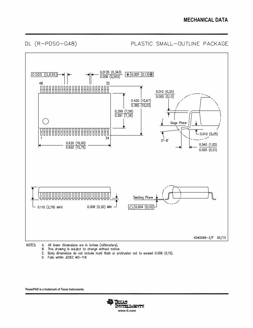
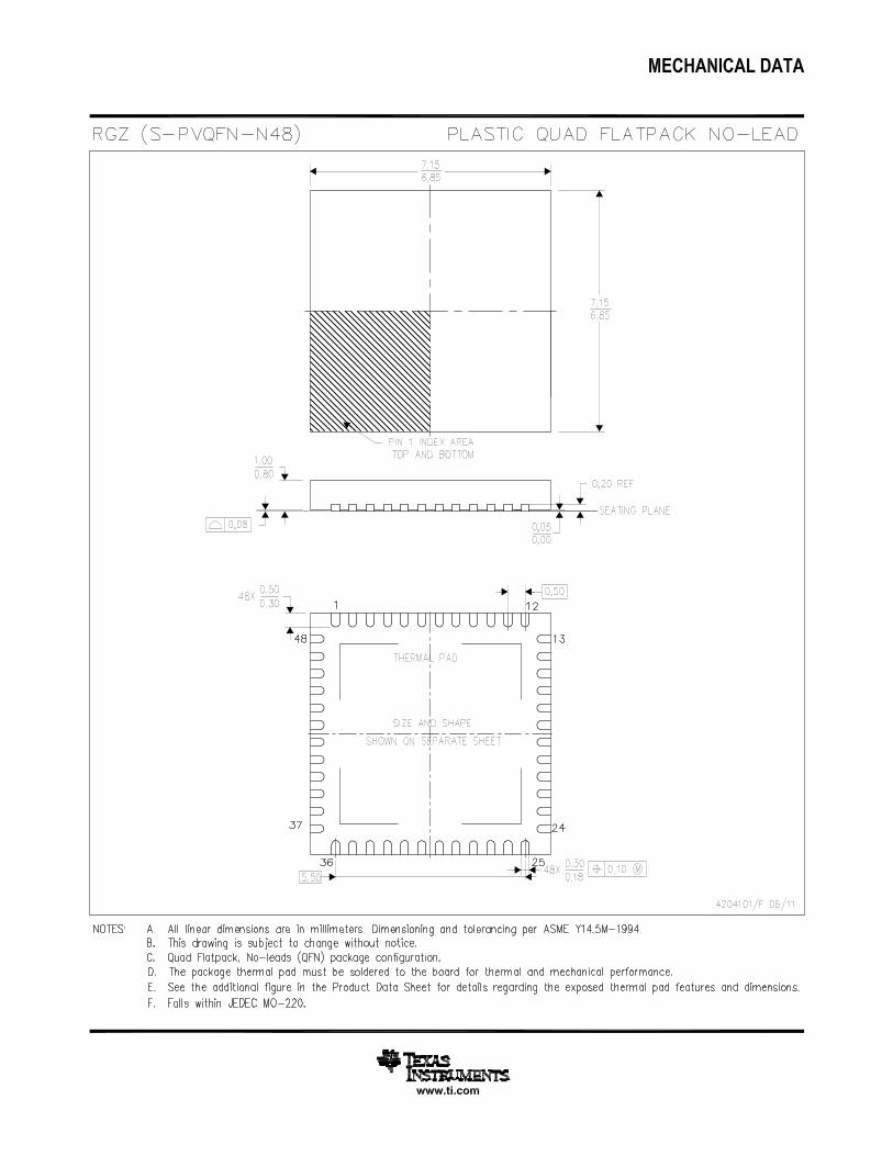

IMPORTANT NOTICE
Texas Instruments Incorporated and its subsidiaries (TI) reserve the right to make corrections, enhancements, improvements and otherchanges to its semiconductor products and services per JESD46, latest issue, and to discontinue any product or service per JESD48, latestissue. Buyers should obtain the latest relevant information before placing orders and should verify that such information is current andcomplete. All semiconductor products (also referred to herein as “components”) are sold subject to TI’s terms and conditions of salesupplied at the time of order acknowledgment.TI warrants performance of its components to the specifications applicable at the time of sale, in accordance with the warranty in TI’s termsand conditions of sale of semiconductor products. Testing and other quality control techniques are used to the extent TI deems necessaryto support this warranty. Except where mandated by applicable law, testing of all parameters of each component is not necessarilyperformed.TI assumes no liability for applications assistance or the design of Buyers’ products. Buyers are responsible for their products andapplications using TI components. To minimize the risks associated with Buyers’ products and applications, Buyers should provideadequate design and operating safeguards.TI does not warrant or represent that any license, either express or implied, is granted under any patent right, copyright, mask work right, orother intellectual property right relating to any combination, machine, or process in which TI components or services are used. Informationpublished by TI regarding third-party products or services does not constitute a license to use such products or services or a warranty orendorsement thereof. Use of such information may require a license from a third party under the patents or other intellectual property of thethird party, or a license from TI under the patents or other intellectual property of TI.Reproduction of significant portions of TI information in TI data books or data sheets is permissible only if reproduction is without alterationand is accompanied by all associated warranties, conditions, limitations, and notices. TI is not responsible or liable for such altereddocumentation. Information of third parties may be subject to additional restrictions.Resale of TI components or services with statements different from or beyond the parameters stated by TI for that component or servicevoids all express and any implied warranties for the associated TI component or service and is an unfair and deceptive business practice.TI is not responsible or liable for any such statements.Buyer acknowledges and agrees that it is solely responsible for compliance with all legal, regulatory and safety-related requirementsconcerning its products, and any use of TI components in its applications, notwithstanding any applications-related information or supportthat may be provided by TI. Buyer represents and agrees that it has all the necessary expertise to create and implement safeguards whichanticipate dangerous consequences of failures, monitor failures and their consequences, lessen the likelihood of failures that might causeharm and take appropriate remedial actions. Buyer will fully indemnify TI and its representatives against any damages arising out of the useof any TI components in safety-critical applications.In some cases, TI components may be promoted specifically to facilitate safety-related applications. With such components, TI’s goal is tohelp enable customers to design and create their own end-product solutions that meet applicable functional safety standards andrequirements. Nonetheless, such components are subject to these terms.No TI components are authorized for use in FDA Class III (or similar life-critical medical equipment) unless authorized officers of the partieshave executed a special agreement specifically governing such use.Only those TI components which TI has specifically designated as military grade or “enhanced plastic” are designed and intended for use inmilitary/aerospace applications or environments. Buyer acknowledges and agrees that any military or aerospace use of TI componentswhich have not been so designated is solely at the Buyer's risk, and that Buyer is solely responsible for compliance with all legal andregulatory requirements in connection with such use.TI has specifically designated certain components as meeting ISO/TS16949 requirements, mainly for automotive use. In any case of use ofnon-designated products, TI will not be responsible for any failure to meet ISO/TS16949.
Products ApplicationsAudio www.ti.com/audio Automotive and Transportation www.ti.com/automotiveAmplifiers amplifier.ti.com Communications and Telecom www.ti.com/communicationsData Converters dataconverter.ti.com Computers and Peripherals www.ti.com/computersDLP® Products www.dlp.com Consumer Electronics www.ti.com/consumer-appsDSP dsp.ti.com Energy and Lighting www.ti.com/energyClocks and Timers www.ti.com/clocks Industrial www.ti.com/industrialInterface interface.ti.com Medical www.ti.com/medicalLogic logic.ti.com Security www.ti.com/securityPower Mgmt power.ti.com Space, Avionics and Defense www.ti.com/space-avionics-defenseMicrocontrollers microcontroller.ti.com Video and Imaging www.ti.com/videoRFID www.ti-rfid.comOMAP Applications Processors www.ti.com/omap TI E2E Community e2e.ti.comWireless Connectivity www.ti.com/wirelessconnectivity
Mailing Address: Texas Instruments, Post Office Box 655303, Dallas, Texas 75265Copyright © 2016, Texas Instruments Incorporated