MSP430F22x2, MSP430F22x4 Mixed Signal Microcontroller (Rev. B
87
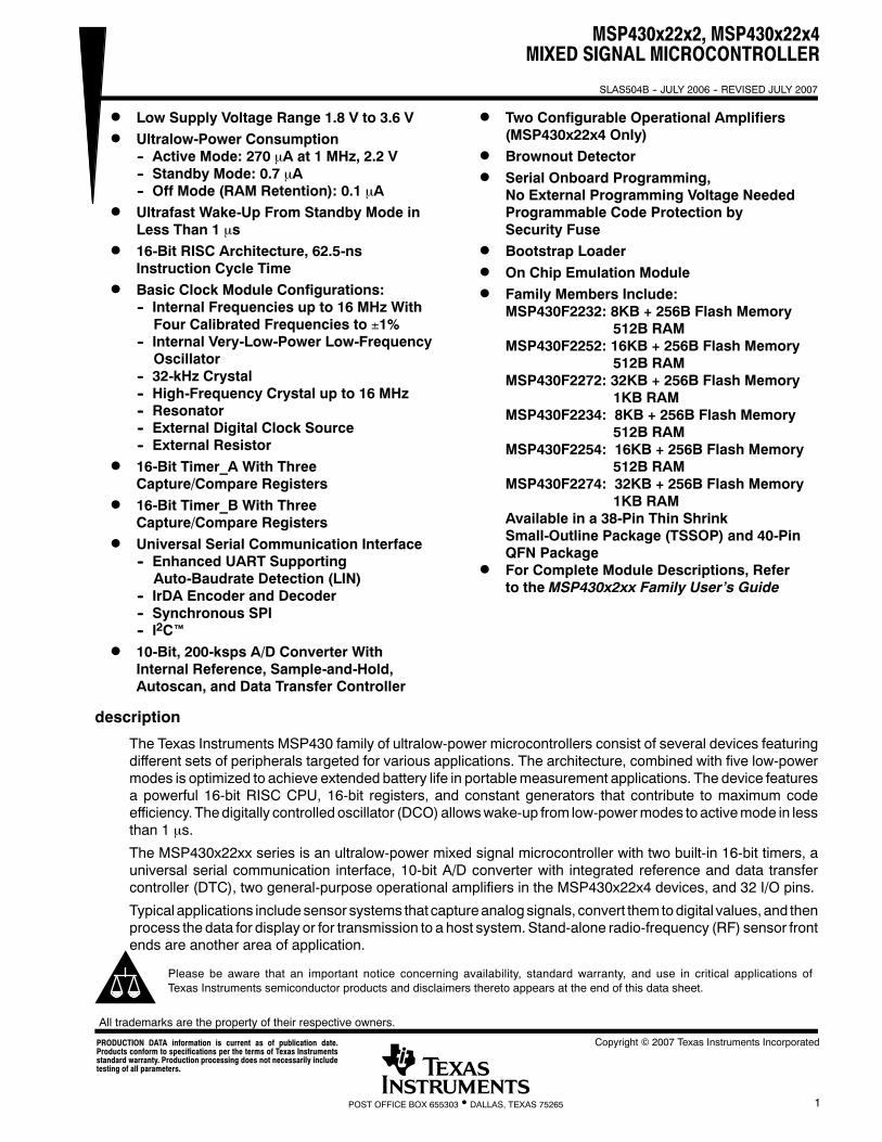
MSP430x22x2, MSP430x22x4 MIXED SIGNAL MICROCONTROLLER SLAS504B -- JULY 2006 -- REVISED JULY 2007 1 POST OFFICE BOX 655303 • DALLAS, TEXAS 75265 D Low Supply Voltage Range 1.8 V to 3.6 V D Ultralow-Power Consumption -- Active Mode: 270 μA at 1 MHz, 2.2 V -- Standby Mode: 0.7 μA -- Off Mode (RAMRetention): 0.1 μA D Ultrafast Wake-Up From Standby Mode in Less Than 1 μs D 16-Bit RISC Architecture, 62.5-ns Instruction Cycle Time D Basic Clock Module Configurations: -- InternalFrequencies up to 16 MHz With Four Calibrated Frequencies to ±1% -- Internal Very-Low-Power Low-Frequency Oscillator -- 32-kHz Crystal -- High-Frequency Crystalup to 16 MHz -- Resonator -- External Digital Clock Source -- External Resistor D 16-Bit Timer_A With Three Capture/Compare Registers D 16-Bit Timer_B With Three Capture/Compare Registers D Universal Serial Communication Interface -- Enhanced UART Supporting Auto-Baudrate Detection (LIN) -- IrDA Encoder and Decoder -- Synchronous SPI -- I 2 C™ D 10-Bit, 200-ksps A/D Converter With Internal Reference, Sample-and-Hold, Autoscan, and Data Transfer Controller D Two Configurable Operational Amplifiers (MSP430x22x4 Only) D Brownout Detector D Serial Onboard Programming, No External Programming Voltage Needed Programmable Code Protection by Security Fuse D Bootstrap Loader D On Chip Emulation Module D Family Members Include: MSP430F2232: 8KB + 256B Flash Memory 512B RAM MSP430F2252: 16KB + 256B Flash Memory 512B RAM MSP430F2272: 32KB + 256B Flash Memory 1KB RAM MSP430F2234: 8KB + 256B Flash Memory 512B RAM MSP430F2254: 16KB + 256B Flash Memory 512B RAM MSP430F2274: 32KB + 256B Flash Memory 1KB RAM Available in a 38-Pin Thin Shrink Small-Outline Package (TSSOP) and 40-Pin QFN Package D For Complete Module Descriptions, Refer to the MSP430x2xx Family User’s Guide description The Texas Instruments MSP430 family of ultralow-power microcontrollers consist of several devices featuring different sets of peripherals targeted for various applications. The architecture, combined with five low-power modes is optimized to achieve extended battery life in portable measurement applications. The device features a powerful 16-bit RISC CPU, 16-bit registers, and constant generators that contribute to maximum code efficiency. The digitally controlled oscillator (DCO) allows wake-up from low-power modes to active mode in less than 1 μs. The MSP430x22xx series is an ultralow-power mixed signal microcontroller with two built-in 16-bit timers, a universal serial communication interface, 10-bit A/D converter with integrated reference and data transfer controller (DTC), two general-purpose operational amplifiers in the MSP430x22x4 devices, and 32 I/O pins. Typical applications include sensor systems that capture analog signals, convert them to digital values, and then process the data for display or for transmission to a host system. Stand-alone radio-frequency (RF) sensor front ends are another area of application. Please be aware that an important notice concerning availability, standard warranty, and use in critical applications of Texas Instruments semiconductor products and disclaimers thereto appears at the end of this data sheet. Copyright © 2007 Texas Instruments Incorporated PRODUCTION DATA information is current as of publication date. Products conform to specifications per the terms of Texas Instruments standard warranty. Production processing does not necessarily include testing of all parameters. All trademarks are the property of their respective owners.
Transcript of MSP430F22x2, MSP430F22x4 Mixed Signal Microcontroller (Rev. B
MSP430x22x2, MSP430x22x4MIXED SIGNAL MICROCONTROLLER
SLAS504B -- JULY 2006 -- REVISED JULY 2007
1POST OFFICE BOX 655303 • DALLAS, TEXAS 75265
D Low Supply Voltage Range 1.8 V to 3.6 VD Ultralow-Power Consumption
-- Active Mode: 270 μA at 1 MHz, 2.2 V-- Standby Mode: 0.7 μA-- Off Mode (RAM Retention): 0.1 μA
D Ultrafast Wake-Up From Standby Mode inLess Than 1 μs
D 16-Bit RISC Architecture, 62.5-nsInstruction Cycle Time
D Basic Clock Module Configurations:-- Internal Frequencies up to 16 MHz WithFour Calibrated Frequencies to ±1%
-- Internal Very-Low-Power Low-FrequencyOscillator
-- 32-kHz Crystal-- High-Frequency Crystal up to 16 MHz-- Resonator-- External Digital Clock Source-- External Resistor
D 16-Bit Timer_A With ThreeCapture/Compare Registers
D 16-Bit Timer_B With ThreeCapture/Compare Registers
D Universal Serial Communication Interface-- Enhanced UART SupportingAuto-Baudrate Detection (LIN)
-- IrDA Encoder and Decoder-- Synchronous SPI-- I2C™
D 10-Bit, 200-ksps A/D Converter WithInternal Reference, Sample-and-Hold,Autoscan, and Data Transfer Controller
D Two Configurable Operational Amplifiers(MSP430x22x4 Only)
D Brownout DetectorD Serial Onboard Programming,
No External Programming Voltage NeededProgrammable Code Protection bySecurity Fuse
D Bootstrap LoaderD On Chip Emulation ModuleD Family Members Include:
MSP430F2232: 8KB + 256B Flash Memory512B RAM
MSP430F2252: 16KB + 256B Flash Memory512B RAM
MSP430F2272: 32KB + 256B Flash Memory1KB RAM
MSP430F2234: 8KB + 256B Flash Memory512B RAM
MSP430F2254: 16KB + 256B Flash Memory512B RAM
MSP430F2274: 32KB + 256B Flash Memory1KB RAM
Available in a 38-Pin Thin ShrinkSmall-Outline Package (TSSOP) and 40-PinQFN Package
D For Complete Module Descriptions, Referto the MSP430x2xx Family User’s Guide
description
The Texas Instruments MSP430 family of ultralow-power microcontrollers consist of several devices featuringdifferent sets of peripherals targeted for various applications. The architecture, combined with five low-powermodes is optimized to achieve extended battery life in portablemeasurement applications. The device featuresa powerful 16-bit RISC CPU, 16-bit registers, and constant generators that contribute to maximum codeefficiency.Thedigitally controlled oscillator (DCO) allowswake-up from low-powermodes to activemode in lessthan 1 μs.
The MSP430x22xx series is an ultralow-power mixed signal microcontroller with two built-in 16-bit timers, auniversal serial communication interface, 10-bit A/D converter with integrated reference and data transfercontroller (DTC), two general-purpose operational amplifiers in the MSP430x22x4 devices, and 32 I/O pins.
Typical applications includesensor systems that captureanalogsignals, convert them todigital values, and thenprocess the data for display or for transmission to a host system.Stand-alone radio-frequency (RF) sensor frontends are another area of application.
Please be aware that an important notice concerning availability, standard warranty, and use in critical applications ofTexas Instruments semiconductor products and disclaimers thereto appears at the end of this data sheet.
Copyright © 2007 Texas Instruments IncorporatedPRODUCTION DATA information is current as of publication date.Products conform to specifications per the terms of Texas Instrumentsstandard warranty. Production processing does not necessarily includetesting of all parameters.
All trademarks are the property of their respective owners.
MSP430x22x2, MSP430x22x4MIXED SIGNAL MICROCONTROLLER
SLAS504B -- JULY 2006 -- REVISED JULY 2007
2 POST OFFICE BOX 655303 • DALLAS, TEXAS 75265
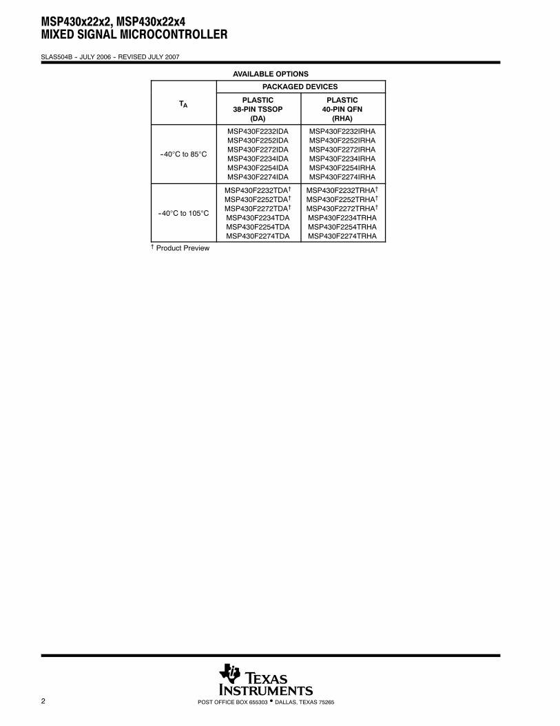
AVAILABLE OPTIONS
PACKAGED DEVICES
TAPLASTIC
38-PIN TSSOP(DA)
PLASTIC40-PIN QFN
(RHA)
--40°C to 85°C
MSP430F2232IDAMSP430F2252IDAMSP430F2272IDAMSP430F2234IDAMSP430F2254IDAMSP430F2274IDA
MSP430F2232IRHAMSP430F2252IRHAMSP430F2272IRHAMSP430F2234IRHAMSP430F2254IRHAMSP430F2274IRHA
--40°C to 105°C
MSP430F2232TDA†
MSP430F2252TDA†
MSP430F2272TDA†
MSP430F2234TDAMSP430F2254TDAMSP430F2274TDA
MSP430F2232TRHA†
MSP430F2252TRHA†
MSP430F2272TRHA†
MSP430F2234TRHAMSP430F2254TRHAMSP430F2274TRHA
† Product Preview
MSP430x22x2, MSP430x22x4MIXED SIGNAL MICROCONTROLLER
SLAS504B -- JULY 2006 -- REVISED JULY 2007
3POST OFFICE BOX 655303 • DALLAS, TEXAS 75265
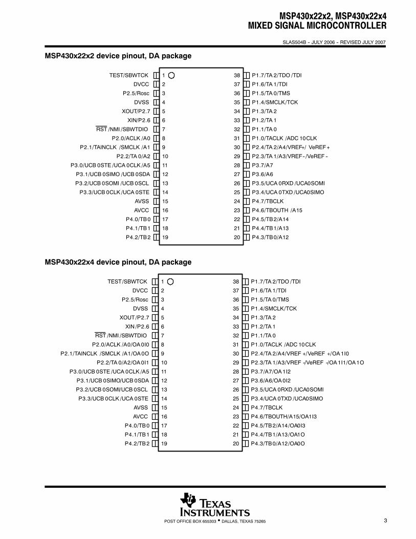
MSP430x22x2 device pinout, DA package
1TEST/SBWTCK
2DVCC
3P2.5/Rosc
4
XOUT/P2.7 5
XIN/P2.6 6
RST /NMI /SBWTDIO 7
P2.0/ACLK /A0 8
P2.1/TAINCLK /SMCLK /A1 9
P2.2/TA 0/A2 10
P3.0/UCB 0STE /UCA 0CLK /A5 11
P3.1/UCB 0SIMO /UCB 0SDA 12
P3.2/UCB 0SOMI /UCB 0SCL 13
P3.3/UCB 0CLK /UCA 0STE 14
P4.0/TB0
15
P4.1/TB1
16
P4.2/TB2
17
P4.3/TB0/A12
18 P4.4/TB1/A13
19
38 P1.7/TA 2/TDO /TDI
37 P1.6/TA 1/TDI
36 P1.5/TA 0/TMS
35 P1.4/SMCLK/TCK
34 P1.3/TA 2
33 P1.2/TA 1
32 P1.1/TA 0
31 P1.0/TACLK /ADC 10CLK
30 P2.4/TA 2/A4/VREF+/ VeREF+
29 P2.3/TA 1/A3/VREF--/VeREF --
28 P3.7/A7
27 P3.6/A6
26 P3.5/UCA 0RXD /UCA0SOMI
25 P3.4/UCA 0TXD /UCA0SIMO
24
23AVCC
22
AVSS
21
P4.7/TBCLK
20
P4.6/TBOUTH /A15
DVSS
P4.5/TB2/A14
MSP430x22x4 device pinout, DA package
1TEST/SBWTCK
2DVCC
3P2.5/Rosc
4
XOUT/P2.7 5
XIN /P2.6 6
RST /NMI /SBWTDIO 7
P2.0/ACLK /A0/OA0I0 8
P2.1/TAINCLK /SMCLK /A1/OA0O 9
P2.2/TA 0/A2/OA0I1 10
P3.0/UCB 0STE /UCA 0CLK /A5 11
P3.1/UCB 0SIMO/UCB 0SDA 12
P3.2/UCB 0SOMI/UCB 0SCL 13
P3.3/UCB 0CLK /UCA 0STE 14
P4.0/TB0
15
P4.1/TB1
16
P4.2/TB2
17
P4.3/TB0/A12/OA0O
18 P4.4/TB1/A13/OA1O
19
38 P1.7/TA 2/TDO /TDI
37 P1.6/TA 1/TDI
36 P1.5/TA 0/TMS
35 P1.4/SMCLK/TCK
34 P1.3/TA 2
33 P1.2/TA 1
32 P1.1/TA 0
31 P1.0/TACLK /ADC 10CLK
30 P2.4/TA 2/A4/VREF +/VeREF +/OA1I0
29 P2.3/TA 1/A3/VREF --/VeREF --/OA1I1/OA1O
28 P3.7/A7/OA1I2
27 P3.6/A6/OA0I2
26 P3.5/UCA 0RXD /UCA0SOMI
25 P3.4/UCA 0TXD /UCA0SIMO
24
23AVCC
22
AVSS
21
P4.7/TBCLK
20
P4.6/TBOUTH/A15/OA1I3
DVSS
P4.5/TB2/A14/OA0I3
MSP430x22x2, MSP430x22x4MIXED SIGNAL MICROCONTROLLER
SLAS504B -- JULY 2006 -- REVISED JULY 2007
4 POST OFFICE BOX 655303 • DALLAS, TEXAS 75265
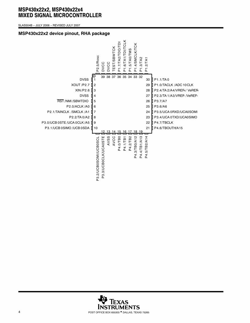
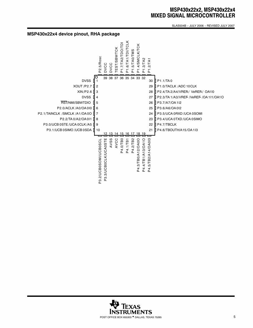
MSP430x22x2 device pinout, RHA package
1DVSS
P1.5/TA0/TMS
P1.0/TACLK /ADC 10CLK
P1.1/TA 0
P1.2/TA1
P1.3/TA2
P1.4/SMCLK/TCK
13
P2.4/TA 2/A4/VREF+/ VeREF+
P2.5/Rosc
DVCC
TEST/SBWTCK
P1.6/TA1/TDI/TCLK
2
3
4
5
6
7
8
10
9
12 14 15 16 17 18 19
30
29
28
27
26
25
24
23
21
22
3839 37 36 35 34 33 32
XOUT /P2.7
XIN /P2.6
DVSS
RST /NMI /SBWTDIO
P2.0/ACLK /A0
P2.1/TAINCLK /SMCLK /A1
P2.2/TA 0/A2
P3.0/UCB 0STE /UCA 0CLK /A5
P3.1/UCB 0SIMO /UCB 0SDA
DVCC
P1.7/TA2/TDO/TDI
P2.3/TA 1/A3/VREF-- /VeREF--
P3.7/A7
P3.6/A6
P3.5/UCA 0RXD/UCA0SOMI
P3.4/UCA 0TXD/UCA0SIMOAVCC
AVSS
P3.2/UCB0SOMI/UCB0SCL
P3.3/UCB0CLK/UCA0STE
P4.0/TB0
P4.1/TB1
P4.2/TB2
P4.3/TB0/A12
P4.4/TB1/A13
P4.5/TB2/A14
P4.6/TBOUTH/A15
P4.7/TBCLK
MSP430x22x2, MSP430x22x4MIXED SIGNAL MICROCONTROLLER
SLAS504B -- JULY 2006 -- REVISED JULY 2007
5POST OFFICE BOX 655303 • DALLAS, TEXAS 75265
MSP430x22x4 device pinout, RHA package
1DVSS
P1.5/TA0/TMS
P1.0/TACLK /ADC 10CLK
P1.1/TA 0
P1.2/TA1
P1.3/TA2
P1.4/SMCLK/TCK
13
P2.4/TA 2/A4/VREF+/ VeREF+/ OA1I0
P2.5/Rosc
DVCC
TEST/SBWTCK
P1.6/TA1/TDI/TCLK
2
3
4
5
6
7
8
10
9
12 14 15 16 17 18 19
30
29
28
27
26
25
24
23
21
22
3839 37 36 35 34 33 32
XOUT /P2.7
XIN /P2.6
DVSS
RST/NMI/SBWTDIO
P2.0/ACLK /A0/OA0I0
P2.1/TAINCLK /SMCLK /A1/OA0O
P2.2/TA 0/A2/OA0I1
P3.0/UCB 0STE /UCA 0CLK /A5
P3.1/UCB 0SIMO /UCB 0SDA
DVCC
P1.7/TA2/TDO/TDI
P2.3/TA 1/A3/VREF-- /VeREF-- /OA1I1/OA1O
P3.7/A7/OA1I2
P3.6/A6/OA0I2
P3.5/UCA 0RXD /UCA 0SOMI
P3.4/UCA 0TXD /UCA 0SIMOAVCC
AVSS
P3.2/UCB0SOMI/UCB0SCL
P3.3/UCB0CLK/UCA0STE
P4.0/TB0
P4.1/TB1
P4.2/TB2
P4.3/TB0/A12/OA0O
P4.4/TB1/A13/OA1O
P4.5/TB2/A14/OA0I3
P4.6/TBOUTH/A15/OA1I3
P4.7/TBCLK
MSP430x22x2, MSP430x22x4MIXED SIGNAL MICROCONTROLLER
SLAS504B -- JULY 2006 -- REVISED JULY 2007
6 POST OFFICE BOX 655303 • DALLAS, TEXAS 75265
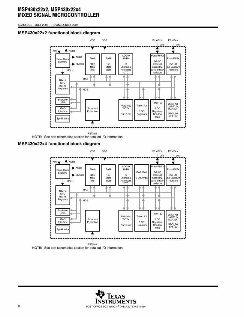
MSP430x22x2 functional block diagram
Basic ClockSystem+
RAM
1kB512B512B
BrownoutProtection
RST/NMI
VCC VSS
MCLK
SMCLK
WatchdogWDT+
15/16--Bit
Timer_A3
3 CCRegisters
16MHzCPUincl. 16Registers
Emulation(2BP)
XOUT
JTAGInterface
Flash
32kB16kB8kB
ACLK
XIN
MDB
MAB
Spy--Bi Wire
Timer_B3
3 CCRegisters,ShadowReg
USCI_A0:UART/LIN,IrDA, SPI
USCI_B0:SPI, I2C
ADC1010--Bit
12Channels,Autoscan,DTC
Ports P1/P2
2x8 I/OInterruptcapability,pull--up/downresistors
Ports P3/P4
2x8 I/Opull--up/downresistors
P1.x/P2.x
2x8
P3.x/P4.x
2x8
NOTE: See port schematics section for detailed I/O information.
MSP430x22x4 functional block diagram
Basic ClockSystem+
RAM
1kB512B512B
BrownoutProtection
RST/NMI
VCC VSS
MCLK
SMCLK
WatchdogWDT+
15/16--Bit
Timer_A3
3 CCRegisters
16MHzCPUincl. 16Registers
Emulation(2BP)
XOUT
JTAGInterface
Flash
32kB16kB8kB
ACLK
XIN
MDB
MAB
Spy--Bi Wire
Timer_B3
3 CCRegisters,ShadowReg
USCI_A0:UART/LIN,IrDA, SPI
USCI_B0:SPI, I2C
OA0, OA1
2 Op Amps
ADC1010--Bit
12Channels,Autoscan,DTC
Ports P1/P2
2x8 I/OInterruptcapability,pull--up/downresistors
Ports P3/P4
2x8 I/Opull--up/downresistors
P1.x/P2.x
2x8
P3.x/P4.x
2x8
NOTE: See port schematics section for detailed I/O information.
MSP430x22x2, MSP430x22x4MIXED SIGNAL MICROCONTROLLER
SLAS504B -- JULY 2006 -- REVISED JULY 2007
7POST OFFICE BOX 655303 • DALLAS, TEXAS 75265
Terminal Functions, MSP430x22x2
TERMINAL
NAMEDA RHA
I/ODESCRIPTION
NAMENO. NO.
I/ODESCRIPTION
P1.0/TACLK/ADC10CLK
31 29 I/O General-purpose digital I/O pinTimer_A, clock signal TACLK inputADC10, conversion clock
P1.1/TA0 32 30 I/O General-purpose digital I/O pinTimer_A, capture: CCI0A input, compare: OUT0 output/BSL transmit
P1.2/TA1 33 31 I/O General-purpose digital I/O pinTimer_A, capture: CCI1A input, compare: OUT1 output
P1.3/TA2 34 32 I/O General-purpose digital I/O pinTimer_A, capture: CCI2A input, compare: OUT2 output
P1.4/SMCLK/TCK
35 33 I/O General-purpose digital I/O pin / SMCLK signal outputTest Clock input for device programming and test
P1.5/TA0/TMS
36 34 I/O General-purpose digital I/O pin / Timer_A, compare: OUT0 outputTest Mode Select input for device programming and test
P1.6/TA1/TDI/TCLK
37 35 I/O General-purpose digital I/O pin / Timer_A, compare: OUT1 outputTest Data Input or Test Clock Input for programming and test
P1.7/TA2/TDO/TDI†
38 36 I/O General-purpose digital I/O pin / Timer_A, compare: OUT2 outputTest Data Output or Test Data Input for programming and test
P2.0/ACLK/A0 8 6 I/O General-purpose digital I/O pin / ACLK outputADC10, analog input A0
P2.1/TAINCLK/SMCLK/A1 9 7 I/O General-purpose digital I/O pinTimer_A, clock signal at INCLK, SMCLK signal outputADC10, analog input A1
P2.2/TA0/A2 10 8 I/O General-purpose digital I/O pinTimer_A, capture: CCI0B input/BSL receive, compare: OUT0 outputADC10, analog input A2
P2.3/TA1/A3/VREF--/VeREF--
29 27 I/O General-purpose digital I/O pinTimer_A, capture CCI1B input, compare: OUT1 outputADC10, analog input A3 / negative reference voltage output/input
P2.4/TA2/A4/VREF+/VeREF+
30 28 I/O General-purpose digital I/O pin / Timer_A, compare: OUT2 outputADC10, analog input A4 / positive reference voltage output/input
P2.5/ROSC
3 40 I/O General-purpose digital I/O pinInput for external DCO resistor to define DCO frequency
XIN/P2.6 6 3 I/O Input terminal of crystal oscillatorGeneral-purpose digital I/O pin
XOUT/P2.7 5 2 I/O Output terminal of crystal oscillatorGeneral-purpose digital I/O pin
P3.0/UCB0STE/UCA0CLK/A5
11 9 I/O General-purpose digital I/O pinUSCI_B0 slave transmit enable / USCI_A0 clock input/outputADC10, analog input A5
P3.1/UCB0SIMO/UCB0SDA
12 10 I/O General-purpose digital I/O pinUSCI_B0 slave in/master out in SPI mode, SDA I2C data in I2C mode
P3.2/UCB0SOMI/UCB0SCL
13 11 I/O General-purpose digital I/O pinUSCI_B0 slave out/master in in SPI mode, SCL I2C clock in I2C mode
P3.3/UCB0CLK/UCA0STE
14 12 I/O General-purpose digital I/O pinUSCI_B0 clock input/output / USCI_A0 slave transmit enable
P3.4/UCA0TXD/UCA0SIMO
25 23 I/O General-purpose digital I/O pinUSCI_A0 transmit dataoutput inUARTmode, slave in/master out inSPImode

MSP430x22x2, MSP430x22x4MIXED SIGNAL MICROCONTROLLER
SLAS504B -- JULY 2006 -- REVISED JULY 2007
8 POST OFFICE BOX 655303 • DALLAS, TEXAS 75265
Terminal Functions, MSP430x22x2 (Continued)
TERMINAL
NAMEDA RHA
I/ODESCRIPTION
NAMENO. NO.
I/ODESCRIPTION
P3.5/UCA0RXD/UCA0SOMI
26 24 I/O General-purpose digital I/O pinUSCI_A0 receive data input in UART mode, slave out/master in in SPI mode
P3.6/A6 27 25 I/O General-purpose digital I/O pinADC10 analog input A6
P3.7/A7 28 26 I/O General-purpose digital I/O pinADC10 analog input A7
P4.0/TB0 17 15 I/O General-purpose digital I/O pinTimer_B, capture: CCI0A input, compare: OUT0 output
P4.1/TB1 18 16 I/O General-purpose digital I/O pinTimer_B, capture: CCI1A input, compare: OUT1 output
P4.2/TB2 19 17 I/O General-purpose digital I/O pinTimer_B, capture: CCI2A input, compare: OUT2 output
P4.3/TB0/A12
20 18 I/O General-purpose digital I/O pinTimer_B, capture: CCI0B input, compare: OUT0 outputADC10 analog input A12
P4.4/TB1A13
21 19 I/O General-purpose digital I/O pinTimer_B, capture: CCI1B input, compare: OUT1 outputADC10 analog input A13
P4.5/TB2A14
22 20 I/O General-purpose digital I/O pinTimer_B, compare: OUT2 outputADC10 analog input A14
P4.6/TBOUTHA15
23 21 I/O General-purpose digital I/O pinTimer_B, switch all TB0 to TB3 outputs to high impedanceADC10 analog input A15
P4.7/TBCLK 24 22 I/O General-purpose digital I/O pinTimer_B, clock signal TBCLK input
RST/NMI/SBWTDIO 7 5 I Reset or nonmaskable interrupt inputSpy-Bi-Wire test data input/output during programming and test
TEST/SBWTCK 1 37 I Selects test mode for JTAG pins on Port1. The device protection fuse isconnected to TEST.Spy-Bi-Wire test clock input during programming and test
DVCC 2 38, 39 Digital supply voltage
AVCC 16 14 Analog supply voltage
DVSS 4 1, 4 Digital ground reference
AVSS 15 13 Analog ground reference
QFN Pad NA PackagePad
NA QFN package pad; connection to DVSS recommended.
† TDO or TDI is selected via JTAG instruction.
NOTE: If XOUT/P2.7/CA7 is usedasan input, excess currentwill flowuntil P2SEL.7 is cleared.This is due to theoscillator output driver connectionto this pad after reset.
MSP430x22x2, MSP430x22x4MIXED SIGNAL MICROCONTROLLER
SLAS504B -- JULY 2006 -- REVISED JULY 2007
9POST OFFICE BOX 655303 • DALLAS, TEXAS 75265
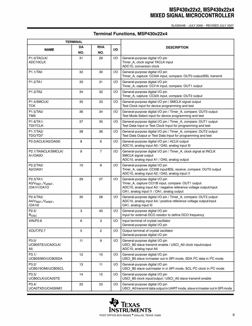
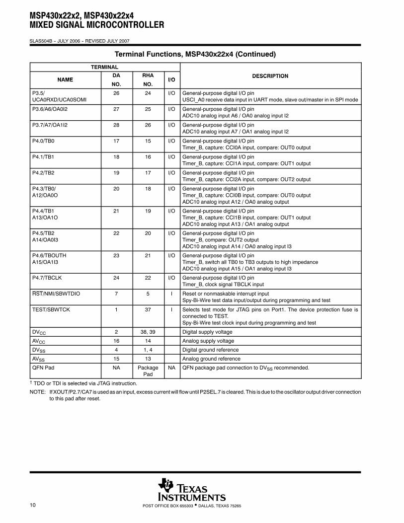
Terminal Functions, MSP430x22x4
TERMINAL
NAMEDA RHA
I/ODESCRIPTION
NAMENO. NO.
I/ODESCRIPTION
P1.0/TACLK/ADC10CLK
31 29 I/O General-purpose digital I/O pinTimer_A, clock signal TACLK inputADC10, conversion clock
P1.1/TA0 32 30 I/O General-purpose digital I/O pinTimer_A, capture: CCI0A input, compare: OUT0 output/BSL transmit
P1.2/TA1 33 31 I/O General-purpose digital I/O pinTimer_A, capture: CCI1A input, compare: OUT1 output
P1.3/TA2 34 32 I/O General-purpose digital I/O pinTimer_A, capture: CCI2A input, compare: OUT2 output
P1.4/SMCLK/TCK
35 33 I/O General-purpose digital I/O pin / SMCLK signal outputTest Clock input for device programming and test
P1.5/TA0/TMS
36 34 I/O General-purpose digital I/O pin / Timer_A, compare: OUT0 outputTest Mode Select input for device programming and test
P1.6/TA1/TDI/TCLK
37 35 I/O General-purpose digital I/O pin / Timer_A, compare: OUT1 outputTest Data Input or Test Clock Input for programming and test
P1.7/TA2/TDO/TDI†
38 36 I/O General-purpose digital I/O pin / Timer_A, compare: OUT2 outputTest Data Output or Test Data Input for programming and test
P2.0/ACLK/A0/OA0I0 8 6 I/O General-purpose digital I/O pin / ACLK outputADC10, analog input A0 / OA0, analog input I0
P2.1/TAINCLK/SMCLK/A1/OA0O
9 7 I/O General-purpose digital I/O pin / Timer_A, clock signal at INCLKSMCLK signal outputADC10, analog input A1 / OA0, analog output
P2.2/TA0/A2/OA0I1
10 8 I/O General-purpose digital I/O pinTimer_A, capture: CCI0B input/BSL receive, compare: OUT0 outputADC10, analog input A2 / OA0, analog input I1
P2.3/TA1/A3/VREF--/VeREF--/OA1I1/OA1O
29 27 I/O General-purpose digital I/O pinTimer_A, capture CCI1B input, compare: OUT1 outputADC10, analog input A3 / negative reference voltage output/inputOA1, analog input I1 / OA1, analog output
P2.4/TA2/A4/VREF+/VeREF+/OA1I0
30 28 I/O General-purpose digital I/O pin / Timer_A, compare: OUT2 outputADC10, analog input A4 / positive reference voltage output/inputOA1, analog input I0
P2.5/ROSC
3 40 I/O General-purpose digital I/O pinInput for external DCO resistor to define DCO frequency
XIN/P2.6 6 3 I/O Input terminal of crystal oscillatorGeneral-purpose digital I/O pin
XOUT/P2.7 5 2 I/O Output terminal of crystal oscillatorGeneral-purpose digital I/O pin
P3.0/UCB0STE/UCA0CLK/A5
11 9 I/O General-purpose digital I/O pinUSCI_B0 slave transmit enable / USCI_A0 clock input/outputADC10, analog input A5
P3.1/UCB0SIMO/UCB0SDA
12 10 I/O General-purpose digital I/O pinUSCI_B0 slave in/master out in SPI mode, SDA I2C data in I2C mode
P3.2/UCB01SOMI/UCB0SCL
13 11 I/O General-purpose digital I/O pinUSCI_B0 slave out/master in in SPI mode, SCL I2C clock in I2C mode
P3.3/UCB0CLK/UCA0STE
14 12 I/O General-purpose digital I/O pinUSCI_B0 clock input/output / USCI_A0 slave transmit enable
P3.4/UCA0TXD/UCA0SIMO
25 23 I/O General-purpose digital I/O pinUSCI_A0 transmit dataoutput inUARTmode, slave in/master out inSPImode
MSP430x22x2, MSP430x22x4MIXED SIGNAL MICROCONTROLLER
SLAS504B -- JULY 2006 -- REVISED JULY 2007
10 POST OFFICE BOX 655303 • DALLAS, TEXAS 75265
Terminal Functions, MSP430x22x4 (Continued)
TERMINAL
NAMEDA RHA
I/ODESCRIPTION
NAMENO. NO.
I/ODESCRIPTION
P3.5/UCA0RXD/UCA0SOMI
26 24 I/O General-purpose digital I/O pinUSCI_A0 receive data input in UART mode, slave out/master in in SPI mode
P3.6/A6/OA0I2 27 25 I/O General-purpose digital I/O pinADC10 analog input A6 / OA0 analog input I2
P3.7/A7/OA1I2 28 26 I/O General-purpose digital I/O pinADC10 analog input A7 / OA1 analog input I2
P4.0/TB0 17 15 I/O General-purpose digital I/O pinTimer_B, capture: CCI0A input, compare: OUT0 output
P4.1/TB1 18 16 I/O General-purpose digital I/O pinTimer_B, capture: CCI1A input, compare: OUT1 output
P4.2/TB2 19 17 I/O General-purpose digital I/O pinTimer_B, capture: CCI2A input, compare: OUT2 output
P4.3/TB0/A12/OA0O
20 18 I/O General-purpose digital I/O pinTimer_B, capture: CCI0B input, compare: OUT0 outputADC10 analog input A12 / OA0 analog output
P4.4/TB1A13/OA1O
21 19 I/O General-purpose digital I/O pinTimer_B, capture: CCI1B input, compare: OUT1 outputADC10 analog input A13 / OA1 analog output
P4.5/TB2A14/OA0I3
22 20 I/O General-purpose digital I/O pinTimer_B, compare: OUT2 outputADC10 analog input A14 / OA0 analog input I3
P4.6/TBOUTHA15/OA1I3
23 21 I/O General-purpose digital I/O pinTimer_B, switch all TB0 to TB3 outputs to high impedanceADC10 analog input A15 / OA1 analog input I3
P4.7/TBCLK 24 22 I/O General-purpose digital I/O pinTimer_B, clock signal TBCLK input
RST/NMI/SBWTDIO 7 5 I Reset or nonmaskable interrupt inputSpy-Bi-Wire test data input/output during programming and test
TEST/SBWTCK 1 37 I Selects test mode for JTAG pins on Port1. The device protection fuse isconnected to TEST.Spy-Bi-Wire test clock input during programming and test
DVCC 2 38, 39 Digital supply voltage
AVCC 16 14 Analog supply voltage
DVSS 4 1, 4 Digital ground reference
AVSS 15 13 Analog ground reference
QFN Pad NA PackagePad
NA QFN package pad connection to DVSS recommended.
† TDO or TDI is selected via JTAG instruction.
NOTE: If XOUT/P2.7/CA7 is usedasan input, excess currentwill flowuntil P2SEL.7 is cleared.This is due to theoscillator output driver connectionto this pad after reset.
General-Purpose Register
Program Counter
Stack Pointer
Status Register
Constant Generator
General-Purpose Register
General-Purpose Register
General-Purpose Register
PC/R0
SP/R1
SR/CG1/R2
CG2/R3
R4
R5
R12
R13
General-Purpose Register
General-Purpose Register
R6
R7
General-Purpose Register
General-Purpose Register
R8
R9
General-Purpose Register
General-Purpose Register
R10
R11
General-Purpose Register
General-Purpose Register
R14
R15
MSP430x22x2, MSP430x22x4MIXED SIGNAL MICROCONTROLLER
SLAS504B -- JULY 2006 -- REVISED JULY 2007
11POST OFFICE BOX 655303 • DALLAS, TEXAS 75265
short-form description
CPU
TheMSP430 CPU has a 16-bit RISC architecturethat is highly transparent to the application. Alloperations, other than program-flow instructions,are performed as register operations inconjunction with seven addressing modes forsource operand and four addressing modes fordestination operand.
The CPU is integrated with 16 registers thatprovide reduced instruction execution time. Theregister-to-register operation execution time isone cycle of the CPU clock.
Four of the registers, R0 to R3, are dedicated asprogram counter, stack pointer, status register,and constant generator respectively. Theremaining registers are general-purposeregisters.
Peripherals are connected to the CPU using data,address, and control buses, and can be handledwith all instructions.
instruction set
The instruction set consists of 51 instructions withthree formats and seven address modes. Eachinstruction can operate on word and byte data.Table 1 shows examples of the three types ofinstruction formats; the address modes are listedin Table 2.
Table 1. Instruction Word Formats
Dual operands, source-destination e.g., ADD R4,R5 R4 + R5 ------> R5
Single operands, destination only e.g., CALL R8 PC ----> (TOS), R8----> PC
Relative jump, un/conditional e.g., JNE Jump-on-equal bit = 0
Table 2. Address Mode Descriptions
ADDRESS MODE S D SYNTAX EXAMPLE OPERATION
Register F F MOV Rs,Rd MOV R10,R11 R10 ----> R11
Indexed F F MOV X(Rn),Y(Rm) MOV 2(R5),6(R6) M(2+R5)----> M(6+R6)
Symbolic (PC relative) F F MOV EDE,TONI M(EDE) ----> M(TONI)
Absolute F F MOV &MEM,&TCDAT M(MEM) ----> M(TCDAT)
Indirect F MOV @Rn,Y(Rm) MOV @R10,Tab(R6) M(R10) ----> M(Tab+R6)
Indirectautoincrement F MOV @Rn+,Rm MOV @R10+,R11
M(R10) ----> R11R10 + 2----> R10
Immediate F MOV #X,TONI MOV #45,TONI #45 ----> M(TONI)
NOTE: S = source D = destination
MSP430x22x2, MSP430x22x4MIXED SIGNAL MICROCONTROLLER
SLAS504B -- JULY 2006 -- REVISED JULY 2007
12 POST OFFICE BOX 655303 • DALLAS, TEXAS 75265
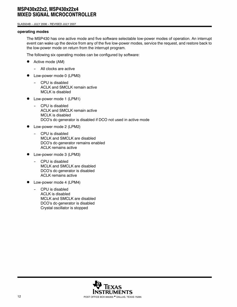
operating modes
The MSP430 has one active mode and five software selectable low-power modes of operation. An interruptevent can wake up the device from any of the five low-power modes, service the request, and restore back tothe low-power mode on return from the interrupt program.
The following six operating modes can be configured by software:
D Active mode (AM)
-- All clocks are active
D Low-power mode 0 (LPM0)
-- CPU is disabledACLK and SMCLK remain activeMCLK is disabled
D Low-power mode 1 (LPM1)
-- CPU is disabledACLK and SMCLK remain activeMCLK is disabledDCO’s dc-generator is disabled if DCO not used in active mode
D Low-power mode 2 (LPM2)
-- CPU is disabledMCLK and SMCLK are disabledDCO’s dc-generator remains enabledACLK remains active
D Low-power mode 3 (LPM3)
-- CPU is disabledMCLK and SMCLK are disabledDCO’s dc-generator is disabledACLK remains active
D Low-power mode 4 (LPM4)
-- CPU is disabledACLK is disabledMCLK and SMCLK are disabledDCO’s dc-generator is disabledCrystal oscillator is stopped
MSP430x22x2, MSP430x22x4MIXED SIGNAL MICROCONTROLLER
SLAS504B -- JULY 2006 -- REVISED JULY 2007
13POST OFFICE BOX 655303 • DALLAS, TEXAS 75265
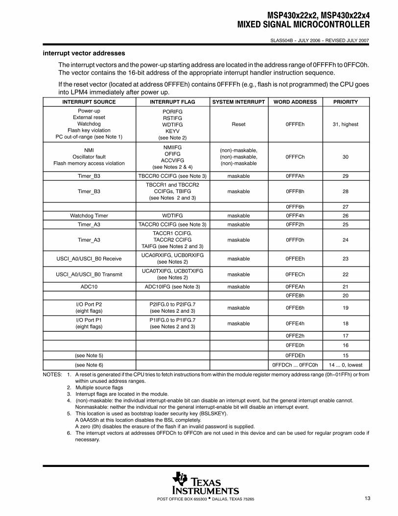
interrupt vector addresses
The interrupt vectors and the power-up starting address are located in the address range of 0FFFFh to 0FFC0h.The vector contains the 16-bit address of the appropriate interrupt handler instruction sequence.
If the reset vector (located at address 0FFFEh) contains 0FFFFh (e.g., flash is not programmed) the CPU goesinto LPM4 immediately after power up.INTERRUPT SOURCE INTERRUPT FLAG SYSTEM INTERRUPT WORD ADDRESS PRIORITY
Power-upExternal resetWatchdog
Flash key violationPC out-of-range (see Note 1)
PORIFGRSTIFGWDTIFGKEYV
(see Note 2)
Reset 0FFFEh 31, highest
NMIOscillator fault
Flash memory access violation
NMIIFGOFIFG
ACCVIFG(see Notes 2 & 4)
(non)-maskable,(non)-maskable,(non)-maskable
0FFFCh 30
Timer_B3 TBCCR0 CCIFG (see Note 3) maskable 0FFFAh 29
Timer_B3TBCCR1 and TBCCR2
CCIFGs, TBIFG(see Notes 2 and 3)
maskable 0FFF8h 28
0FFF6h 27
Watchdog Timer WDTIFG maskable 0FFF4h 26
Timer_A3 TACCR0 CCIFG (see Note 3) maskable 0FFF2h 25
Timer_A3TACCR1 CCIFG.TACCR2 CCIFG
TAIFG (see Notes 2 and 3)maskable 0FFF0h 24
USCI_A0/USCI_B0 ReceiveUCA0RXIFG, UCB0RXIFG
(see Notes 2) maskable 0FFEEh 23
USCI_A0/USCI_B0 TransmitUCA0TXIFG, UCB0TXIFG
(see Notes 2) maskable 0FFECh 22
ADC10 ADC10IFG (see Note 3) maskable 0FFEAh 21
0FFE8h 20
I/O Port P2(eight flags)
P2IFG.0 to P2IFG.7(see Notes 2 and 3) maskable 0FFE6h 19
I/O Port P1(eight flags)
P1IFG.0 to P1IFG.7(see Notes 2 and 3) maskable 0FFE4h 18
0FFE2h 17
0FFE0h 16
(see Note 5) 0FFDEh 15
(see Note 6) 0FFDCh ... 0FFC0h 14 ... 0, lowest
NOTES: 1. A reset is generated if the CPU tries to fetch instructions fromwithin themodule register memory address range (0h--01FFh) or fromwithin unused address ranges.
2. Multiple source flags3. Interrupt flags are located in the module.4. (non)-maskable: the individual interrupt-enable bit can disable an interrupt event, but the general interrupt enable cannot.
Nonmaskable: neither the individual nor the general interrupt-enable bit will disable an interrupt event.5. This location is used as bootstrap loader security key (BSLSKEY).
A 0AA55h at this location disables the BSL completely.A zero (0h) disables the erasure of the flash if an invalid password is supplied.
6. The interrupt vectors at addresses 0FFDCh to 0FFC0h are not used in this device and can be used for regular program code ifnecessary.
MSP430x22x2, MSP430x22x4MIXED SIGNAL MICROCONTROLLER
SLAS504B -- JULY 2006 -- REVISED JULY 2007
14 POST OFFICE BOX 655303 • DALLAS, TEXAS 75265
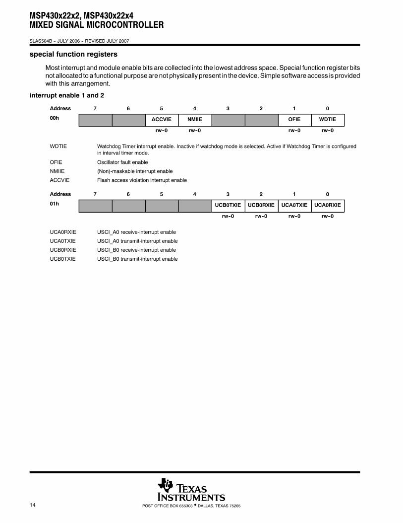
special function registers
Most interrupt andmodule enable bits are collected into the lowest address space. Special function register bitsnot allocated toa functional purposearenot physically present in thedevice.Simple softwareaccess is providedwith this arrangement.
interrupt enable 1 and 2
Address 7 6 5 4 3 2 1 0
00h ACCVIE NMIIE OFIE WDTIE
rw--0 rw--0 rw--0 rw--0
WDTIE Watchdog Timer interrupt enable. Inactive if watchdog mode is selected. Active if Watchdog Timer is configuredin interval timer mode.
OFIE Oscillator fault enable
NMIIE (Non)-maskable interrupt enable
ACCVIE Flash access violation interrupt enable
Address 7 6 5 4 3 2 1 0
01h UCB0TXIE UCB0RXIE UCA0TXIE UCA0RXIE
rw--0 rw--0 rw--0 rw--0
UCA0RXIE USCI_A0 receive-interrupt enable
UCA0TXIE USCI_A0 transmit-interrupt enable
UCB0RXIE USCI_B0 receive-interrupt enable
UCB0TXIE USCI_B0 transmit-interrupt enable
MSP430x22x2, MSP430x22x4MIXED SIGNAL MICROCONTROLLER
SLAS504B -- JULY 2006 -- REVISED JULY 2007
15POST OFFICE BOX 655303 • DALLAS, TEXAS 75265
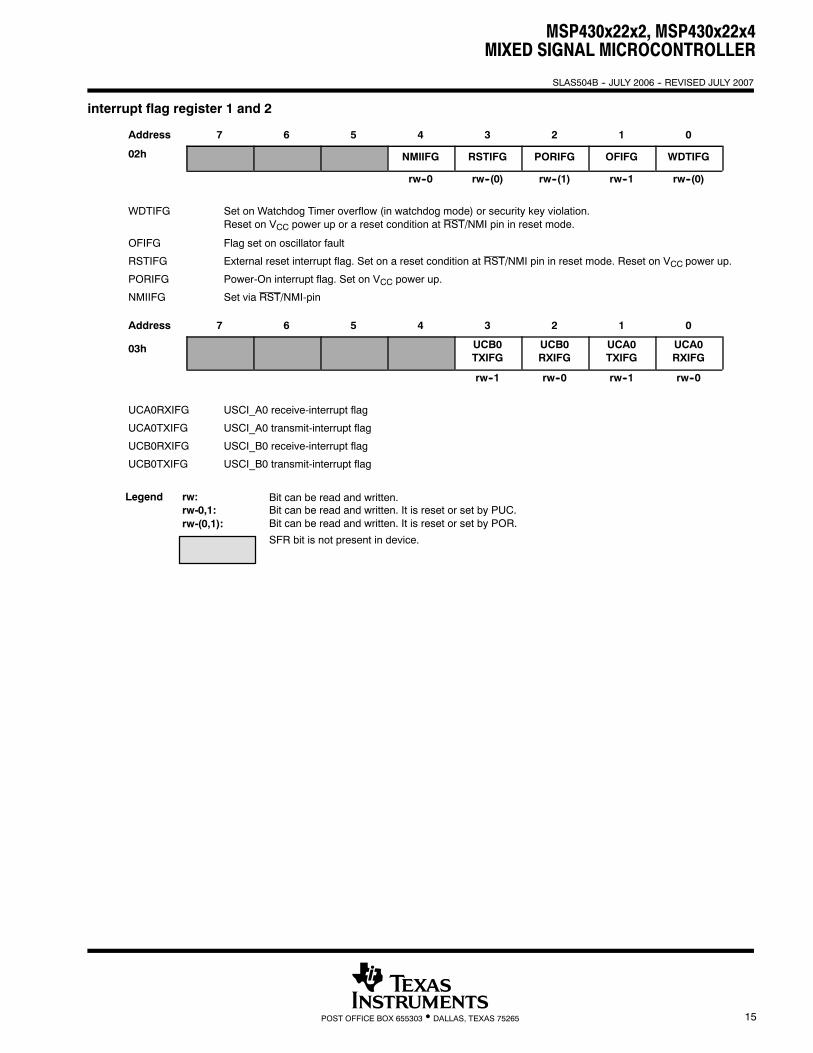
interrupt flag register 1 and 2
Address 7 6 5 4 3 2 1 0
02h NMIIFG RSTIFG PORIFG OFIFG WDTIFG
rw--0 rw--(0) rw--(1) rw--1 rw--(0)
WDTIFG Set on Watchdog Timer overflow (in watchdog mode) or security key violation.Reset on VCC power up or a reset condition at RST/NMI pin in reset mode.
OFIFG Flag set on oscillator fault
RSTIFG External reset interrupt flag. Set on a reset condition at RST/NMI pin in reset mode. Reset on VCC power up.
PORIFG Power-On interrupt flag. Set on VCC power up.
NMIIFG Set via RST/NMI-pin
Address 7 6 5 4 3 2 1 0
03h UCB0TXIFG
UCB0RXIFG
UCA0TXIFG
UCA0RXIFG
rw--1 rw--0 rw--1 rw--0
UCA0RXIFG USCI_A0 receive-interrupt flag
UCA0TXIFG USCI_A0 transmit-interrupt flag
UCB0RXIFG USCI_B0 receive-interrupt flag
UCB0TXIFG USCI_B0 transmit-interrupt flag
Legend rw:rw-0,1:
Bit can be read and written.Bit can be read and written. It is reset or set by PUC.Bit can be read and written. It is reset or set by POR.rw-(0,1):
SFR bit is not present in device.
MSP430x22x2, MSP430x22x4MIXED SIGNAL MICROCONTROLLER
SLAS504B -- JULY 2006 -- REVISED JULY 2007
16 POST OFFICE BOX 655303 • DALLAS, TEXAS 75265
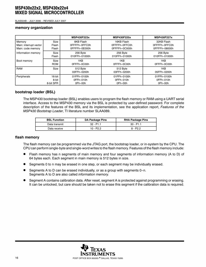
memory organization
MSP430F223x MSP430F225x MSP430F227x
MemoryMain: interrupt vectorMain: code memory
SizeFlashFlash
8KB Flash0FFFFh--0FFC0h0FFFFh--0E000h
16KB Flash0FFFFh--0FFC0h0FFFFh--0C000h
32KB Flash0FFFFh--0FFC0h0FFFFh--08000h
Information memory SizeFlash
256 Byte010FFh--01000h
256 Byte010FFh--01000h
256 Byte010FFh--01000h
Boot memory SizeROM
1KB0FFFh--0C00h
1KB0FFFh--0C00h
1KB0FFFh--0C00h
RAM Size 512 Byte03FFh--0200h
512 Byte03FFh--0200h
1KB05FFh--0200h
Peripherals 16-bit8-bit
8-bit SFR
01FFh--0100h0FFh--010h0Fh--00h
01FFh--0100h0FFh--010h0Fh--00h
01FFh--0100h0FFh--010h0Fh--00h
bootstrap loader (BSL)
The MSP430 bootstrap loader (BSL) enables users to program the flash memory or RAM using a UART serialinterface. Access to the MSP430 memory via the BSL is protected by user-defined password. For completedescription of the features of the BSL and its implementation, see the application report, Features of theMSP430 Bootstrap Loader, TI literature number SLAA089.
BSL Function DA Package Pins RHA Package Pins
Data transmit 32 - P1.1 30 - P1.1
Data receive 10 - P2.2 8 - P2.2
flash memory
The flash memory can be programmed via the JTAG port, the bootstrap loader, or in-system by the CPU. TheCPUcan performsingle-byte and single-wordwrites to the flashmemory. Features of the flashmemory include:
D Flash memory has n segments of main memory and four segments of information memory (A to D) of64 bytes each. Each segment in main memory is 512 bytes in size.
D Segments 0 to n may be erased in one step, or each segment may be individually erased.
D Segments A to D can be erased individually, or as a group with segments 0--n.Segments A to D are also called information memory.
D Segment A contains calibration data. After reset, segment A is protected against programming or erasing.It can be unlocked, but care should be taken not to erase this segment if the calibration data is required.
MSP430x22x2, MSP430x22x4MIXED SIGNAL MICROCONTROLLER
SLAS504B -- JULY 2006 -- REVISED JULY 2007
17POST OFFICE BOX 655303 • DALLAS, TEXAS 75265
peripherals
Peripherals are connected to the CPU through data, address, and control busses and can be handled usingall instructions. For complete module descriptions, refer to the MSP430x2xx Family User’s Guide.
oscillator and system clock
The clock system is supported by the basic clock module that includes support for a 32768-Hz watch crystaloscillator, an internal very low power, low frequency oscillator, an internal digitally-controlled oscillator (DCO),and a high frequency crystal oscillator. The basic clock module is designed to meet the requirements of bothlow system cost and low power consumption. The internal DCO provides a fast turn-on clock source andstabilizes in less than 1 μs. The basic clock module provides the following clock signals:
D Auxiliary clock (ACLK), sourced froma32768-Hzwatch crystal, a high frequency crystal, or the internal verylow power LF oscillator.
D Main clock (MCLK), the system clock used by the CPU.D Sub-Main clock (SMCLK), the sub-system clock used by the peripheral modules.
DCO Calibration Data (provided from factory in flash info memory segment A)
DCO Frequency Calibration Register Size Address
1 MHz CALBC1_1MHZ byte 010FFh
CALDCO_1MHZ byte 010FEh
8 MHz CALBC1_8MHZ byte 010FDh
CALDCO_8MHZ byte 010FCh
12 MHz CALBC1_12MHZ byte 010FBh
CALDCO_12MHZ byte 010FAh
16 MHz CALBC1_16MHZ byte 010F9h
CALDCO_16MHZ byte 010F8h
brownout
The brownout circuit is implemented to provide the proper internal reset signal to the device during power onand power off.
digital I/O
There are four 8-bit I/O ports implemented—ports P1, P2, P3, and P4:
D All individual I/O bits are independently programmable.D Any combination of input, output, and interrupt conditions is possible.D Edge-selectable interrupt input capability for all the eight bits of port P1 and P2.D Read/write access to port-control registers is supported by all instructions.D Each I/O has an individually programmable pullup/pulldown resistor.
watchdog timer (WDT+)
The primary function of the WDT+ module is to perform a controlled system restart after a software problemoccurs. If the selected time interval expires, a system reset is generated. If the watchdog function is not neededin an application, themodule can be configured as an interval timer and can generate interrupts at selected timeintervals.
MSP430x22x2, MSP430x22x4MIXED SIGNAL MICROCONTROLLER
SLAS504B -- JULY 2006 -- REVISED JULY 2007
18 POST OFFICE BOX 655303 • DALLAS, TEXAS 75265
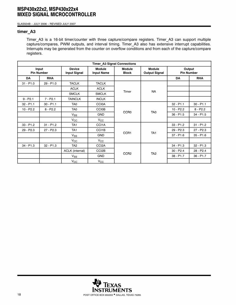
timer_A3
Timer_A3 is a 16-bit timer/counter with three capture/compare registers. Timer_A3 can support multiplecapture/compares, PWM outputs, and interval timing. Timer_A3 also has extensive interrupt capabilities.Interrupts may be generated from the counter on overflow conditions and from each of the capture/compareregisters.
Timer_A3 Signal Connections
InputPin Number
DeviceInput Signal
ModuleInput Name
ModuleBlock
ModuleOutput Signal
OutputPin Number
DA RHA DA RHA
31 - P1.0 29 - P1.0 TACLK TACLK
ACLK ACLKTimer NA
SMCLK SMCLKTimer NA
9 - P2.1 7 - P2.1 TAINCLK INCLK
32 - P1.1 30 - P1.1 TA0 CCI0A 32 - P1.1 30 - P1.1
10 - P2.2 8 - P2.2 TA0 CCI0BCCR0 TA0
10 - P2.2 8 - P2.2
VSS GNDCCR0 TA0
36 - P1.5 34 - P1.5
VCC VCC33 - P1.2 31 - P1.2 TA1 CCI1A 33 - P1.2 31 - P1.2
29 - P2.3 27 - P2.3 TA1 CCI1BCCR1 TA1
29 - P2.3 27 - P2.3
VSS GNDCCR1 TA1
37 - P1.6 35 - P1.6
VCC VCC34 - P1.3 32 - P1.3 TA2 CCI2A 34 - P1.3 32 - P1.3
ACLK (internal) CCI2BCCR2 TA2
30 - P2.4 28 - P2.4
VSS GNDCCR2 TA2
38 - P1.7 36 - P1.7
VCC VCC
MSP430x22x2, MSP430x22x4MIXED SIGNAL MICROCONTROLLER
SLAS504B -- JULY 2006 -- REVISED JULY 2007
19POST OFFICE BOX 655303 • DALLAS, TEXAS 75265
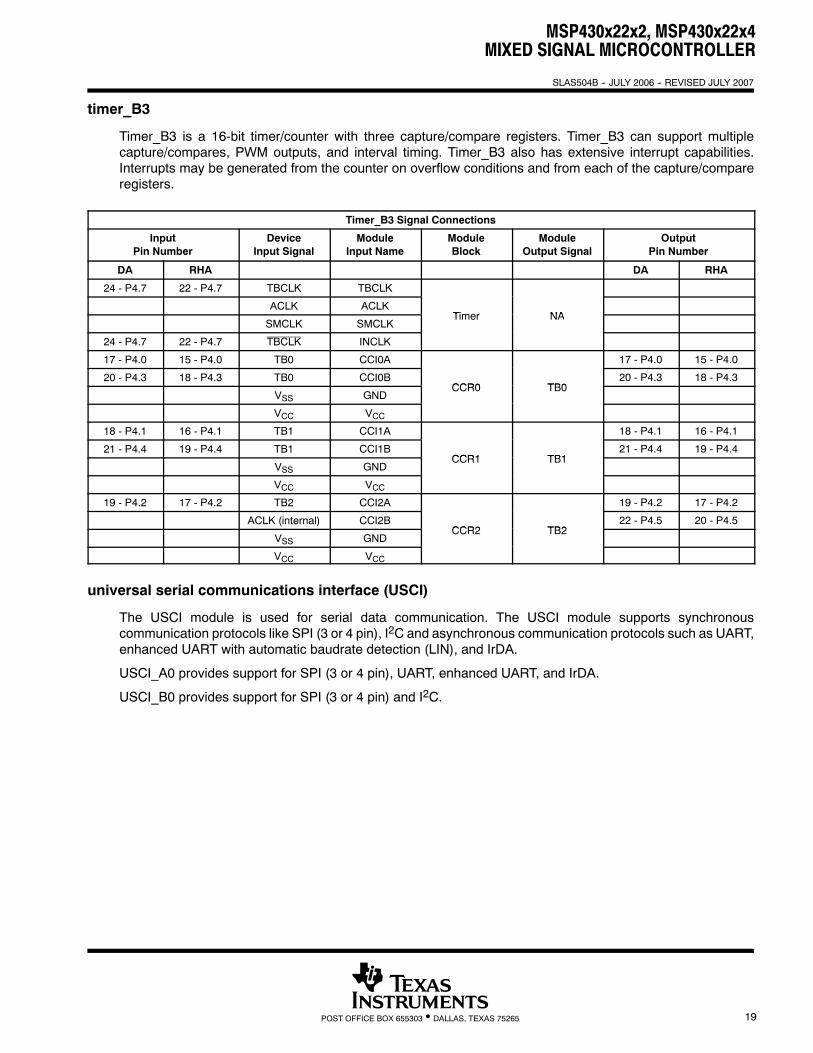
timer_B3
Timer_B3 is a 16-bit timer/counter with three capture/compare registers. Timer_B3 can support multiplecapture/compares, PWM outputs, and interval timing. Timer_B3 also has extensive interrupt capabilities.Interrupts may be generated from the counter on overflow conditions and from each of the capture/compareregisters.
Timer_B3 Signal Connections
InputPin Number
DeviceInput Signal
ModuleInput Name
ModuleBlock
ModuleOutput Signal
OutputPin Number
DA RHA DA RHA
24 - P4.7 22 - P4.7 TBCLK TBCLK
ACLK ACLKTimer NA
SMCLK SMCLKTimer NA
24 - P4.7 22 - P4.7 TBCLK INCLK
17 - P4.0 15 - P4.0 TB0 CCI0A 17 - P4.0 15 - P4.0
20 - P4.3 18 - P4.3 TB0 CCI0BCCR0 TB0
20 - P4.3 18 - P4.3
VSS GNDCCR0 TB0
VCC VCC18 - P4.1 16 - P4.1 TB1 CCI1A 18 - P4.1 16 - P4.1
21 - P4.4 19 - P4.4 TB1 CCI1BCCR1 TB1
21 - P4.4 19 - P4.4
VSS GNDCCR1 TB1
VCC VCC19 - P4.2 17 - P4.2 TB2 CCI2A 19 - P4.2 17 - P4.2
ACLK (internal) CCI2BCCR2 TB2
22 - P4.5 20 - P4.5
VSS GNDCCR2 TB2
VCC VCC
universal serial communications interface (USCI)
The USCI module is used for serial data communication. The USCI module supports synchronouscommunication protocols like SPI (3 or 4 pin), I2C and asynchronous communication protocols such as UART,enhanced UART with automatic baudrate detection (LIN), and IrDA.
USCI_A0 provides support for SPI (3 or 4 pin), UART, enhanced UART, and IrDA.
USCI_B0 provides support for SPI (3 or 4 pin) and I2C.
MSP430x22x2, MSP430x22x4MIXED SIGNAL MICROCONTROLLER
SLAS504B -- JULY 2006 -- REVISED JULY 2007
20 POST OFFICE BOX 655303 • DALLAS, TEXAS 75265
ADC10The ADC10 module supports fast, 10-bit analog-to-digital conversions. The module implements a 10-bit SARcore, sample select control, reference generator and data transfer controller, or DTC, for automatic conversionresult handling allowing ADC samples to be converted and stored without any CPU intervention.
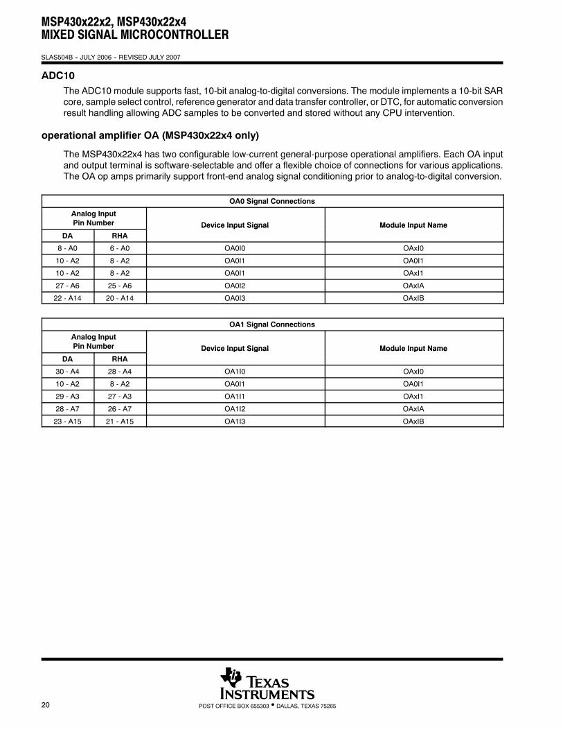
operational amplifier OA (MSP430x22x4 only)
The MSP430x22x4 has two configurable low-current general-purpose operational amplifiers. Each OA inputand output terminal is software-selectable and offer a flexible choice of connections for various applications.The OA op amps primarily support front-end analog signal conditioning prior to analog-to-digital conversion.
OA0 Signal Connections
Analog InputPin Number Device Input Signal Module Input Name
DA RHADevice Input Signal Module Input Name
8 - A0 6 - A0 OA0I0 OAxI0
10 - A2 8 - A2 OA0I1 OA0I1
10 - A2 8 - A2 OA0I1 OAxI1
27 - A6 25 - A6 OA0I2 OAxIA
22 - A14 20 - A14 OA0I3 OAxIB
OA1 Signal Connections
Analog InputPin Number Device Input Signal Module Input Name
DA RHADevice Input Signal Module Input Name
30 - A4 28 - A4 OA1I0 OAxI0
10 - A2 8 - A2 OA0I1 OA0I1
29 - A3 27 - A3 OA1I1 OAxI1
28 - A7 26 - A7 OA1I2 OAxIA
23 - A15 21 - A15 OA1I3 OAxIB
MSP430x22x2, MSP430x22x4MIXED SIGNAL MICROCONTROLLER
SLAS504B -- JULY 2006 -- REVISED JULY 2007
21POST OFFICE BOX 655303 • DALLAS, TEXAS 75265
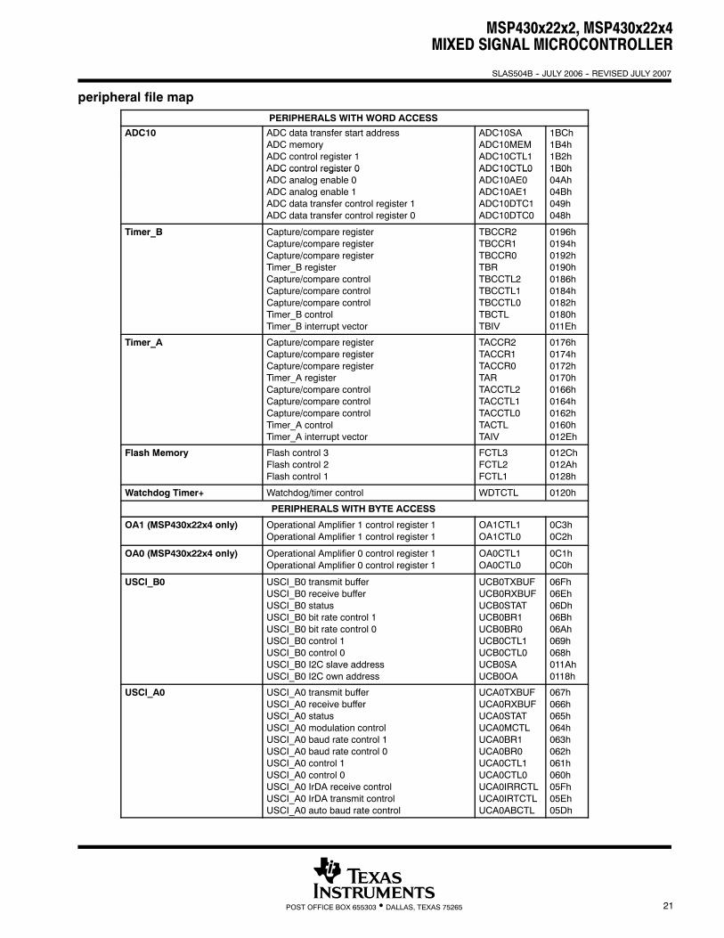
peripheral file map
PERIPHERALS WITH WORD ACCESS
ADC10 ADC data transfer start addressADC memoryADC control register 1ADC control register 0
ADC10SAADC10MEMADC10CTL1ADC10CTL0
1BCh1B4h1B2h1B0hADC control register 0
ADC analog enable 0ADC analog enable 1ADC data transfer control register 1ADC data transfer control register 0
ADC10CTL0ADC10AE0ADC10AE1ADC10DTC1ADC10DTC0
1B0h04Ah04Bh049h048h
Timer_B Capture/compare registerCapture/compare registerCapture/compare registerTimer_B registerCapture/compare controlCapture/compare controlCapture/compare controlTimer_B controlTimer_B interrupt vector
TBCCR2TBCCR1TBCCR0TBRTBCCTL2TBCCTL1TBCCTL0TBCTLTBIV
0196h0194h0192h0190h0186h0184h0182h0180h011Eh
Timer_A Capture/compare registerCapture/compare registerCapture/compare registerTimer_A registerCapture/compare controlCapture/compare controlCapture/compare controlTimer_A controlTimer_A interrupt vector
TACCR2TACCR1TACCR0TARTACCTL2TACCTL1TACCTL0TACTLTAIV
0176h0174h0172h0170h0166h0164h0162h0160h012Eh
Flash Memory Flash control 3Flash control 2Flash control 1
FCTL3FCTL2FCTL1
012Ch012Ah0128h
Watchdog Timer+ Watchdog/timer control WDTCTL 0120h
PERIPHERALS WITH BYTE ACCESS
OA1 (MSP430x22x4 only) Operational Amplifier 1 control register 1Operational Amplifier 1 control register 1
OA1CTL1OA1CTL0
0C3h0C2h
OA0 (MSP430x22x4 only) Operational Amplifier 0 control register 1Operational Amplifier 0 control register 1
OA0CTL1OA0CTL0
0C1h0C0h
USCI_B0 USCI_B0 transmit bufferUSCI_B0 receive bufferUSCI_B0 statusUSCI_B0 bit rate control 1USCI_B0 bit rate control 0USCI_B0 control 1USCI_B0 control 0USCI_B0 I2C slave addressUSCI_B0 I2C own address
UCB0TXBUFUCB0RXBUFUCB0STATUCB0BR1UCB0BR0UCB0CTL1UCB0CTL0UCB0SAUCB0OA
06Fh06Eh06Dh06Bh06Ah069h068h011Ah0118h
USCI_A0 USCI_A0 transmit bufferUSCI_A0 receive bufferUSCI_A0 statusUSCI_A0 modulation controlUSCI_A0 baud rate control 1USCI_A0 baud rate control 0USCI_A0 control 1USCI_A0 control 0USCI_A0 IrDA receive controlUSCI_A0 IrDA transmit controlUSCI_A0 auto baud rate control
UCA0TXBUFUCA0RXBUFUCA0STATUCA0MCTLUCA0BR1UCA0BR0UCA0CTL1UCA0CTL0UCA0IRRCTLUCA0IRTCTLUCA0ABCTL
067h066h065h064h063h062h061h060h05Fh05Eh05Dh
MSP430x22x2, MSP430x22x4MIXED SIGNAL MICROCONTROLLER
SLAS504B -- JULY 2006 -- REVISED JULY 2007
22 POST OFFICE BOX 655303 • DALLAS, TEXAS 75265
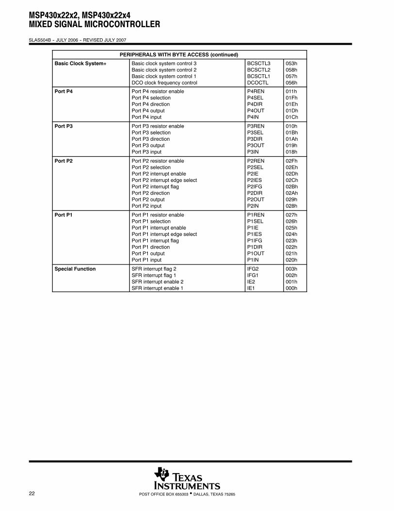
PERIPHERALS WITH BYTE ACCESS (continued)
Basic Clock System+ Basic clock system control 3Basic clock system control 2Basic clock system control 1DCO clock frequency control
BCSCTL3BCSCTL2BCSCTL1DCOCTL
053h058h057h056h
Port P4 Port P4 resistor enablePort P4 selectionPort P4 directionPort P4 outputPort P4 input
P4RENP4SELP4DIRP4OUTP4IN
011h01Fh01Eh01Dh01Ch
Port P3 Port P3 resistor enablePort P3 selectionPort P3 directionPort P3 outputPort P3 input
P3RENP3SELP3DIRP3OUTP3IN
010h01Bh01Ah019h018h
Port P2 Port P2 resistor enablePort P2 selectionPort P2 interrupt enablePort P2 interrupt edge selectPort P2 interrupt flagPort P2 directionPort P2 outputPort P2 input
P2RENP2SELP2IEP2IESP2IFGP2DIRP2OUTP2IN
02Fh02Eh02Dh02Ch02Bh02Ah029h028h
Port P1 Port P1 resistor enablePort P1 selectionPort P1 interrupt enablePort P1 interrupt edge selectPort P1 interrupt flagPort P1 directionPort P1 outputPort P1 input
P1RENP1SELP1IEP1IESP1IFGP1DIRP1OUTP1IN
027h026h025h024h023h022h021h020h
Special Function SFR interrupt flag 2SFR interrupt flag 1SFR interrupt enable 2SFR interrupt enable 1
IFG2IFG1IE2IE1
003h002h001h000h
MSP430x22x2, MSP430x22x4MIXED SIGNAL MICROCONTROLLER
SLAS504B -- JULY 2006 -- REVISED JULY 2007
23POST OFFICE BOX 655303 • DALLAS, TEXAS 75265
absolute maximum ratings (see Note 1)Voltage applied at VCC to VSS --0.3 V to 4.1 V. . . . . . . . . . . . . . . . . . . . . . . . . . . . . . . . . . . . . . . . . . . . . . . . . . . . . .Voltage applied to any pin (see Note 2) --0.3 V to VCC+0.3 V. . . . . . . . . . . . . . . . . . . . . . . . . . . . . . . . . . . . . . . .Diode current at any device terminal ±2 mA. . . . . . . . . . . . . . . . . . . . . . . . . . . . . . . . . . . . . . . . . . . . . . . . . . . . . . .Storage temperature range, Tstg (unprogrammed device, see Note 3) --55°C to 150°C. . . . . . . . . . . . . . . . . .Storage temperature range, Tstg (programmed device, see Note 3) --40°C to 105°C. . . . . . . . . . . . . . . . . . . .
NOTES: 1. Stresses beyond those listed under “absolute maximum ratings” may cause permanent damage to the device. These are stressratings only, and functional operation of the device at these or any other conditions beyond those indicated under “recommendedoperating conditions” is not implied. Exposure to absolute-maximum-rated conditions for extended periods may affect devicereliability.
2. All voltages referenced to VSS. The JTAG fuse-blow voltage, VFB, is allowed to exceed the absolute maximum rating. The voltageis applied to the TEST pin when blowing the JTAG fuse.
3. Higher temperature may be applied during board soldering process according to the current JEDEC J-STD-020 specification withpeak reflow temperatures not higher than classified on the device label on the shipping boxes or reels.
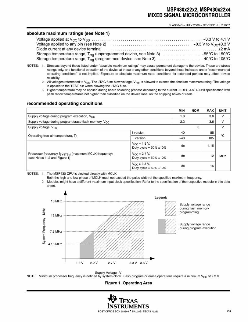
recommended operating conditions
MIN NOM MAX UNIT
Supply voltage during program execution, VCC 1.8 3.6 V
Supply voltage during program/erase flash memory, VCC 2.2 3.6 V
Supply voltage, VSS 0 V
Operating free air temperature TI version --40 85
°COperating free-air temperature, TA T version --40 105°C
VCC = 1.8 V,Duty cycle = 50% ±10% dc 4.15
Processor frequency fSYSTEM (maximum MCLK frequency)(see Notes 1, 2 and Figure 1)
VCC = 2.7 V,Duty cycle = 50% ±10% dc 12 MHz
VCC ≥ 3.3 V,Duty cycle = 50% ±10% dc 16
NOTES: 1. The MSP430 CPU is clocked directly with MCLK.Both the high and low phase of MCLK must not exceed the pulse width of the specified maximum frequency.
2. Modules might have a different maximum input clock specification. Refer to the specification of the respective module in this datasheet.
4.15 MHz
12 MHz
16 MHz
1.8 V 2.2 V 2.7 V 3.3 V 3.6 V
Supply Voltage --V
SystemFrequency--M
Hz
Supply voltage range,during flash memoryprogramming
Supply voltage range,during program execution
Legend:
7.5 MHz
NOTE: Minimum processor frequency is defined by system clock. Flash program or erase operations require a minimum VCC of 2.2 V.
Figure 1. Operating Area
MSP430x22x2, MSP430x22x4MIXED SIGNAL MICROCONTROLLER
SLAS504B -- JULY 2006 -- REVISED JULY 2007
24 POST OFFICE BOX 655303 • DALLAS, TEXAS 75265
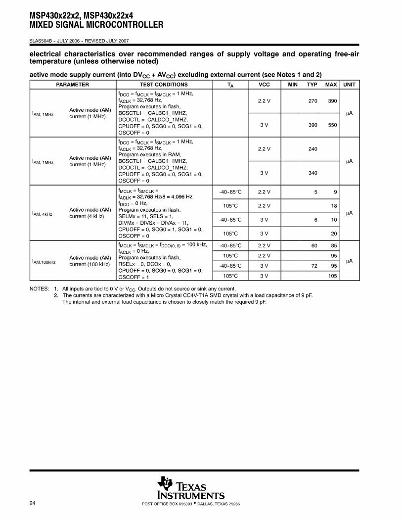
electrical characteristics over recommended ranges of supply voltage and operating free-airtemperature (unless otherwise noted)
active mode supply current (into DVCC + AVCC) excluding external current (see Notes 1 and 2)PARAMETER TEST CONDITIONS TA VCC MIN TYP MAX UNIT
I Active mode (AM)
fDCO = fMCLK = fSMCLK = 1 MHz,fACLK = 32,768 Hz,Program executes in flash,BCSCTL1 CALBC1 1MHZ
2.2 V 270 390
μAIAM, 1MHzActive mode (AM)current (1 MHz)
BCSCTL1 = CALBC1_1MHZ,DCOCTL = CALDCO_1MHZ,CPUOFF = 0, SCG0 = 0, SCG1 = 0,OSCOFF = 0
3 V 390 550
μA
I Active mode (AM)
fDCO = fMCLK = fSMCLK = 1 MHz,fACLK = 32,768 Hz,Program executes in RAM,BCSCTL1 CALBC1 1MHZ
2.2 V 240
μAIAM, 1MHzActive mode (AM)current (1 MHz)
BCSCTL1 = CALBC1_1MHZ,DCOCTL = CALDCO_1MHZ,CPUOFF = 0, SCG0 = 0, SCG1 = 0,OSCOFF = 0
3 V 340
μA
fMCLK = fSMCLK =fACLK = 32,768 Hz/8 = 4,096 Hz,
-40--85°C 2.2 V 5 9
I Active mode (AM)
fACLK = 32,768 Hz/8 = 4,096 Hz,fDCO = 0 Hz,Program executes in flash,
105°C 2.2 V 18μAIAM, 4kHz
Active mode (AM)current (4 kHz)
Program executes in flash,SELMx = 11, SELS = 1,DIVMx = DIVSx = DIVAx = 11, -40--85°C 3 V 6 10
μA
DIVMx DIVSx DIVAx 11,CPUOFF = 0, SCG0 = 1, SCG1 = 0,OSCOFF = 0 105°C 3 V 20
fMCLK = fSMCLK = fDCO(0, 0) ≈ 100 kHz,f 0 Hz
-40--85°C 2.2 V 60 85
I Active mode (AM)fACLK = 0 Hz,Program executes in flash, 105°C 2.2 V 95
μAIAM,100kHzActive mode (AM)current (100 kHz)
Program executes in flash,RSELx = 0, DCOx = 0,CPUOFF = 0 SCG0 = 0 SCG1 = 0
-40--85°C 3 V 72 95μA
CPUOFF = 0, SCG0 = 0, SCG1 = 0,OSCOFF = 1 105°C 3 V 105
NOTES: 1. All inputs are tied to 0 V or VCC. Outputs do not source or sink any current.2. The currents are characterized with a Micro Crystal CC4V-T1A SMD crystal with a load capacitance of 9 pF.
The internal and external load capacitance is chosen to closely match the required 9 pF.
MSP430x22x2, MSP430x22x4MIXED SIGNAL MICROCONTROLLER
SLAS504B -- JULY 2006 -- REVISED JULY 2007
25POST OFFICE BOX 655303 • DALLAS, TEXAS 75265
electrical characteristics over recommended ranges of supply voltage and operating free-airtemperature (unless otherwise noted) (continued)
typical characteristics -- active mode supply current (into DVCC + AVCC)
0.0
1.0
2.0
3.0
4.0
5.0
6.0
7.0
8.0
1.5 2.0 2.5 3.0 3.5 4.0
VCC -- Supply Voltage -- V
ActiveModeCurrent--mA
Figure 2. Active Mode Current vs VCC, TA = 25°C
fDCO = 1 MHz
fDCO = 8 MHz
fDCO = 12 MHz
fDCO = 16 MHz
0.0
1.0
2.0
3.0
4.0
5.0
0.0 4.0 8.0 12.0 16.0
fDCO -- DCO Frequency -- MHz
ActiveModeCurrent--mA
Figure 3. Active Mode Current vs DCO Frequency
TA = 25 °C
TA = 85 °C
VCC = 2.2 V
VCC = 3 V
TA = 25 °C
TA = 85 °C
MSP430x22x2, MSP430x22x4MIXED SIGNAL MICROCONTROLLER
SLAS504B -- JULY 2006 -- REVISED JULY 2007
26 POST OFFICE BOX 655303 • DALLAS, TEXAS 75265
electrical characteristics over recommended ranges of supply voltage and operating free-airtemperature (unless otherwise noted) (continued)
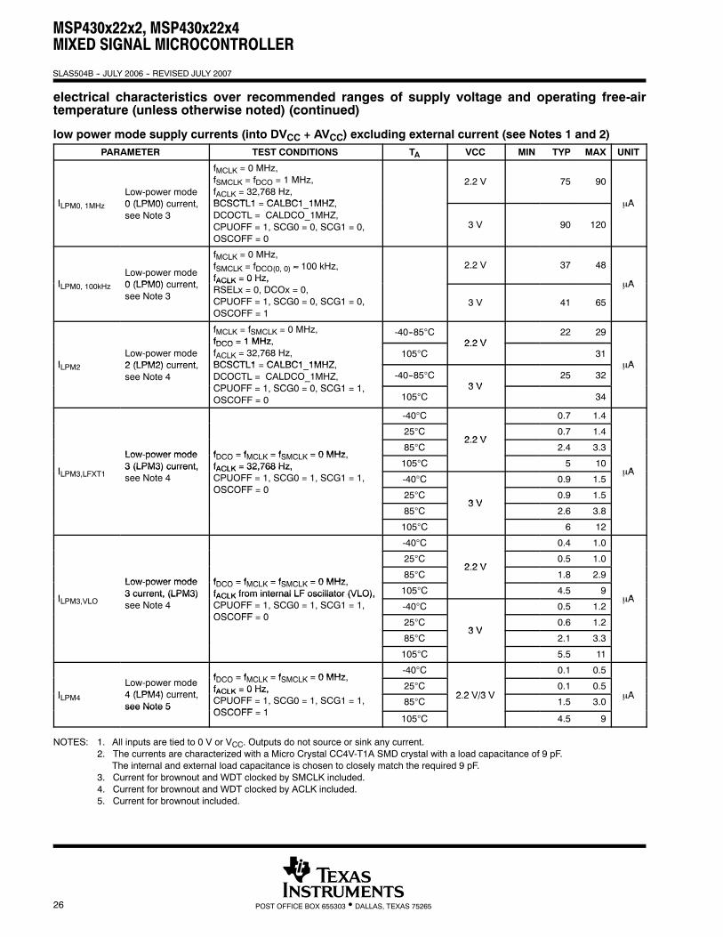
low power mode supply currents (into DVCC + AVCC) excluding external current (see Notes 1 and 2)PARAMETER TEST CONDITIONS TA VCC MIN TYP MAX UNIT
ILow-power mode0 (LPM0) current
fMCLK = 0 MHz,fSMCLK = fDCO = 1 MHz,fACLK = 32,768 Hz,BCSCTL1 CALBC1 1MHZ
2.2 V 75 90
μAILPM0, 1MHz 0 (LPM0) current,see Note 3
BCSCTL1 = CALBC1_1MHZ,DCOCTL = CALDCO_1MHZ,CPUOFF = 1, SCG0 = 0, SCG1 = 0,OSCOFF = 0
3 V 90 120
μA
ILow-power mode0 (LPM0) current
fMCLK = 0 MHz,fSMCLK = fDCO(0, 0) ≈ 100 kHz,fACLK = 0 Hz,
2.2 V 37 48
μAILPM0, 100kHz 0 (LPM0) current,see Note 3
fACLK = 0 Hz,RSELx = 0, DCOx = 0,CPUOFF = 1, SCG0 = 0, SCG1 = 0,OSCOFF = 1
3 V 41 65
μA
fMCLK = fSMCLK = 0 MHz,fDCO = 1 MHz
-40--85°C2 2 V
22 29
ILow-power mode2 (LPM2) current
fDCO = 1 MHz,fACLK = 32,768 Hz,BCSCTL1 CALBC1 1MHZ
105°C2.2 V
31μAILPM2 2 (LPM2) current,
see Note 4BCSCTL1 = CALBC1_1MHZ,DCOCTL = CALDCO_1MHZ,CPUOFF 1 SCG0 0 SCG1 1
-40--85°C3 V
25 32μA
_CPUOFF = 1, SCG0 = 0, SCG1 = 1,OSCOFF = 0 105°C
3 V34
-40°C 0.7 1.4
25°C2 2 V
0.7 1.4
Low-power mode fDCO = fMCLK = fSMCLK = 0 MHz85°C
2.2 V2.4 3.3
I
Low-power mode3 (LPM3) current,
fDCO = fMCLK = fSMCLK = 0 MHz,fACLK = 32,768 Hz, 105°C 5 10
μAILPM3,LFXT13 (LPM3) current,see Note 4
fACLK = 32,768 Hz,CPUOFF = 1, SCG0 = 1, SCG1 = 1,OSCOFF 0
-40°C 0.9 1.5μA
OSCOFF = 0 25°C3 V
0.9 1.5
85°C3 V
2.6 3.8
105°C 6 12
-40°C 0.4 1.0
25°C2 2 V
0.5 1.0
Low-power mode fDCO = fMCLK = fSMCLK = 0 MHz85°C
2.2 V1.8 2.9
I
Low-power mode3 current, (LPM3)
fDCO = fMCLK = fSMCLK = 0 MHz,fACLK from internal LF oscillator (VLO), 105°C 4.5 9
μAILPM3,VLO3 current, (LPM3)see Note 4
fACLK from internal LF oscillator (VLO),CPUOFF = 1, SCG0 = 1, SCG1 = 1,OSCOFF 0
-40°C 0.5 1.2μA
OSCOFF = 0 25°C3 V
0.6 1.2
85°C3 V
2.1 3.3
105°C 5.5 11
fDCO = fMCLK = fSMCLK = 0 MHz-40°C 0.1 0.5
ILow-power mode4 (LPM4) current
fDCO = fMCLK = fSMCLK = 0 MHz,fACLK = 0 Hz, 25°C
2 2 V/3 V0.1 0.5
AILPM4 4 (LPM4) current,see Note 5
fACLK = 0 Hz,CPUOFF = 1, SCG0 = 1, SCG1 = 1,OSCOFF 1
85°C2.2 V/3 V
1.5 3.0μA
see Note 5OSCOFF = 1
105°C 4.5 9
NOTES: 1. All inputs are tied to 0 V or VCC. Outputs do not source or sink any current.2. The currents are characterized with a Micro Crystal CC4V-T1A SMD crystal with a load capacitance of 9 pF.
The internal and external load capacitance is chosen to closely match the required 9 pF.3. Current for brownout and WDT clocked by SMCLK included.4. Current for brownout and WDT clocked by ACLK included.5. Current for brownout included.
MSP430x22x2, MSP430x22x4MIXED SIGNAL MICROCONTROLLER
SLAS504B -- JULY 2006 -- REVISED JULY 2007
27POST OFFICE BOX 655303 • DALLAS, TEXAS 75265
electrical characteristics over recommended ranges of supply voltage and operating free-airtemperature (unless otherwise noted) (continued)
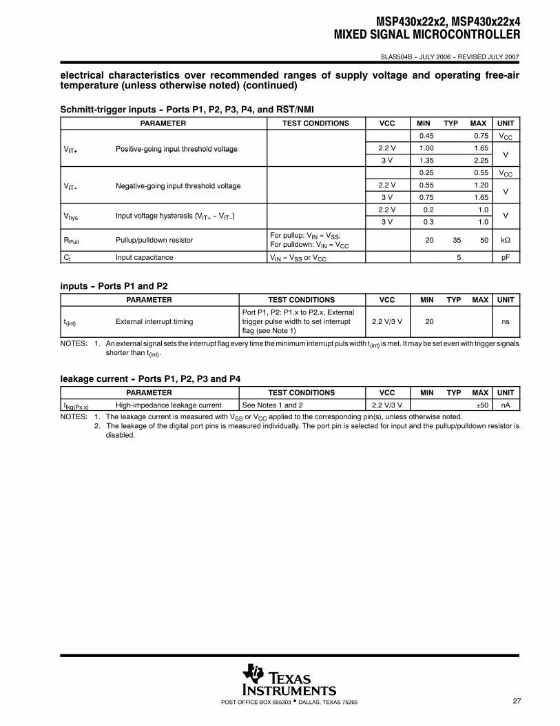
Schmitt-trigger inputs -- Ports P1, P2, P3, P4, and RST/NMIPARAMETER TEST CONDITIONS VCC MIN TYP MAX UNIT
0.45 0.75 VCC
VIT+ Positive-going input threshold voltage 2.2 V 1.00 1.65V
VIT+ Positive going input threshold voltage
3 V 1.35 2.25V
0.25 0.55 VCC
VIT-- Negative-going input threshold voltage 2.2 V 0.55 1.20V
VIT-- Negative going input threshold voltage
3 V 0.75 1.65V
V Input voltage hysteresis (V V )2.2 V 0.2 1.0
VVhys Input voltage hysteresis (VIT+ -- VIT--)3 V 0.3 1.0
V
RPull Pullup/pulldown resistorFor pullup: VIN = VSS;For pulldown: VIN = VCC
20 35 50 kΩ
CI Input capacitance VIN = VSS or VCC 5 pF
inputs -- Ports P1 and P2PARAMETER TEST CONDITIONS VCC MIN TYP MAX UNIT
t(int) External interrupt timingPort P1, P2: P1.x to P2.x, Externaltrigger pulse width to set interruptflag (see Note 1)
2.2 V/3 V 20 ns
NOTES: 1. Anexternal signal sets the interrupt flag every time theminimum interrupt pulswidth t(int) ismet. Itmay be set evenwith trigger signalsshorter than t(int).
leakage current -- Ports P1, P2, P3 and P4PARAMETER TEST CONDITIONS VCC MIN TYP MAX UNIT
Ilkg(Px.x) High-impedance leakage current See Notes 1 and 2 2.2 V/3 V ±50 nA
NOTES: 1. The leakage current is measured with VSS or VCC applied to the corresponding pin(s), unless otherwise noted.2. The leakage of the digital port pins is measured individually. The port pin is selected for input and the pullup/pulldown resistor is
disabled.
MSP430x22x2, MSP430x22x4MIXED SIGNAL MICROCONTROLLER
SLAS504B -- JULY 2006 -- REVISED JULY 2007
28 POST OFFICE BOX 655303 • DALLAS, TEXAS 75265
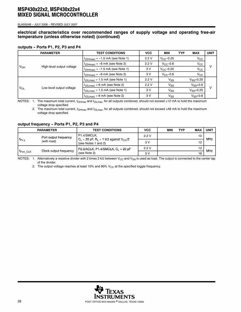
electrical characteristics over recommended ranges of supply voltage and operating free-airtemperature (unless otherwise noted) (continued)
outputs -- Ports P1, P2, P3 and P4PARAMETER TEST CONDITIONS VCC MIN TYP MAX UNIT
I(OHmax) = --1.5 mA (see Note 1) 2.2 V VCC--0.25 VCC
V High level output voltageI(OHmax) = --6 mA (see Note 2) 2.2 V VCC--0.6 VCC
VVOH High-level output voltageI(OHmax) = --1.5 mA (see Note 1) 3 V VCC--0.25 VCC
V
I(OHmax) = --6 mA (see Note 2) 3 V VCC--0.6 VCCI(OLmax) = 1.5 mA (see Note 1) 2.2 V VSS VSS+0.25
V Low level output voltageI(OLmax) = 6 mA (see Note 2) 2.2 V VSS VSS+0.6
VVOL Low-level output voltageI(OLmax) = 1.5 mA (see Note 1) 3 V VSS VSS+0.25
V
I(OLmax) = 6 mA (see Note 2) 3 V VSS VSS+0.6
NOTES: 1. The maximum total current, IOHmax and IOLmax, for all outputs combined, should not exceed ±12 mA to hold the maximumvoltage drop specified.
2. The maximum total current, IOHmax and IOLmax, for all outputs combined, should not exceed ±48 mA to hold the maximumvoltage drop specified.
output frequency -- Ports P1, P2, P3 and P4PARAMETER TEST CONDITIONS VCC MIN TYP MAX UNIT
f Port output frequency P1.4/SMCLK,C 20 pF R 1 kΩ against V /2
2.2 V 10MHzfPx.y
Port output frequency(with load) CL = 20 pF, RL = 1 kΩ against VCC/2
(see Notes 1 and 2) 3 V 12MHz
f Clock output frequency P2.0/ACLK, P1.4/SMCLK, CL = 20 pF 2.2 V 12MHzfPort_CLK Clock output frequency P2.0/ACLK, P1.4/SMCLK, CL = 20 pF
(see Note 2) 3 V 16MHz
NOTES: 1. Alternatively a resistive divider with 2 times 2 kΩ between VCC and VSS is used as load. The output is connected to the center tapof the divider.
2. The output voltage reaches at least 10% and 90% VCC at the specified toggle frequency.
MSP430x22x2, MSP430x22x4MIXED SIGNAL MICROCONTROLLER
SLAS504B -- JULY 2006 -- REVISED JULY 2007
29POST OFFICE BOX 655303 • DALLAS, TEXAS 75265
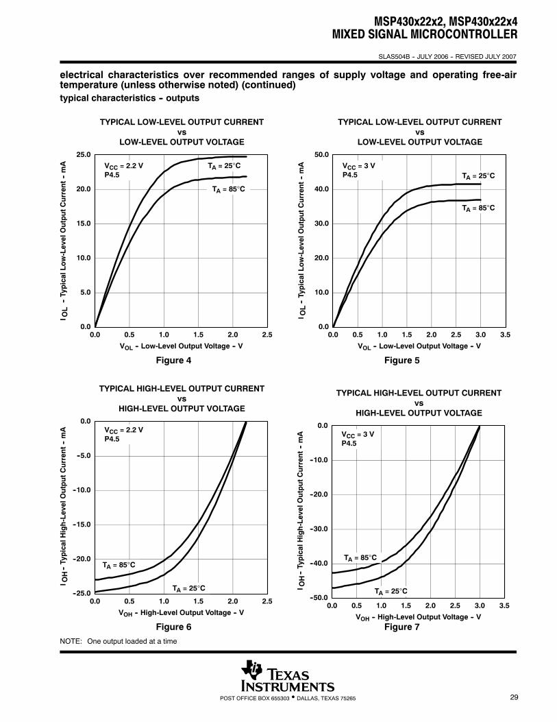
electrical characteristics over recommended ranges of supply voltage and operating free-airtemperature (unless otherwise noted) (continued)typical characteristics -- outputs
Figure 4
VOL -- Low-Level Output Voltage -- V
0.0
5.0
10.0
15.0
20.0
25.0
0.0 0.5 1.0 1.5 2.0 2.5
VCC = 2.2 VP4.5
TYPICAL LOW-LEVEL OUTPUT CURRENTvs
LOW-LEVEL OUTPUT VOLTAGE
TA = 25°C
TA = 85°C
OL
I--TypicalLow-LevelOutputCurrent--mA
Figure 5
VOL -- Low-Level Output Voltage -- V
0.0
10.0
20.0
30.0
40.0
50.0
0.0 0.5 1.0 1.5 2.0 2.5 3.0 3.5
VCC = 3 VP4.5
TYPICAL LOW-LEVEL OUTPUT CURRENTvs
LOW-LEVEL OUTPUT VOLTAGE
TA = 25°C
TA = 85°C
OL
I--TypicalLow-LevelOutputCurrent--mA
Figure 6
VOH -- High-Level Output Voltage -- V
--25.0
--20.0
--15.0
--10.0
--5.0
0.0
0.0 0.5 1.0 1.5 2.0 2.5
VCC = 2.2 VP4.5
TYPICAL HIGH-LEVEL OUTPUT CURRENTvs
HIGH-LEVEL OUTPUT VOLTAGE
TA = 25°C
TA = 85°C
OH
I--TypicalHigh-LevelOutputCurrent--mA
Figure 7VOH -- High-Level Output Voltage -- V
--50.0
--40.0
--30.0
--20.0
--10.0
0.0
0.0 0.5 1.0 1.5 2.0 2.5 3.0 3.5
VCC = 3 VP4.5
TYPICAL HIGH-LEVEL OUTPUT CURRENTvs
HIGH-LEVEL OUTPUT VOLTAGE
TA = 25°C
TA = 85°C
OH
I--TypicalHigh-LevelOutputCurrent--mA
NOTE: One output loaded at a time
MSP430x22x2, MSP430x22x4MIXED SIGNAL MICROCONTROLLER
SLAS504B -- JULY 2006 -- REVISED JULY 2007
30 POST OFFICE BOX 655303 • DALLAS, TEXAS 75265
electrical characteristics over recommended ranges of supply voltage and operating free-airtemperature (unless otherwise noted) (continued)
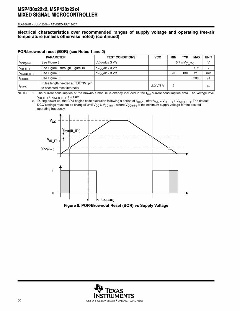
POR/brownout reset (BOR) (see Notes 1 and 2)PARAMETER TEST CONDITIONS VCC MIN TYP MAX UNIT
VCC(start) See Figure 8 dVCC/dt ≤ 3 V/s 0.7 × V(B_IT--) V
V(B_IT--) See Figure 8 through Figure 10 dVCC/dt ≤ 3 V/s 1.71 V
Vhys(B_IT--) See Figure 8 dVCC/dt ≤ 3 V/s 70 130 210 mV
td(BOR) See Figure 8 2000 μs
t(reset)Pulse length needed at RST/NMI pinto accepted reset internally
2.2 V/3 V 2 μs
NOTES: 1. The current consumption of the brownout module is already included in the ICC current consumption data. The voltage levelV(B_IT--) + Vhys(B_IT--) is ≤ 1.8V.
2. During power up, the CPU begins code execution following a period of td(BOR) after VCC = V(B_IT--) + Vhys(B_IT--). The defaultDCO settings must not be changed until VCC ≥ VCC(min), where VCC(min) is the minimum supply voltage for the desiredoperating frequency.
0
1
t d(BOR)
VCC
V(B_IT--)
Vhys(B_IT--)
VCC(start)
Figure 8. POR/Brownout Reset (BOR) vs Supply Voltage
MSP430x22x2, MSP430x22x4MIXED SIGNAL MICROCONTROLLER
SLAS504B -- JULY 2006 -- REVISED JULY 2007
31POST OFFICE BOX 655303 • DALLAS, TEXAS 75265
electrical characteristics over recommended ranges of supply voltage and operating free-airtemperature (unless otherwise noted) (continued)
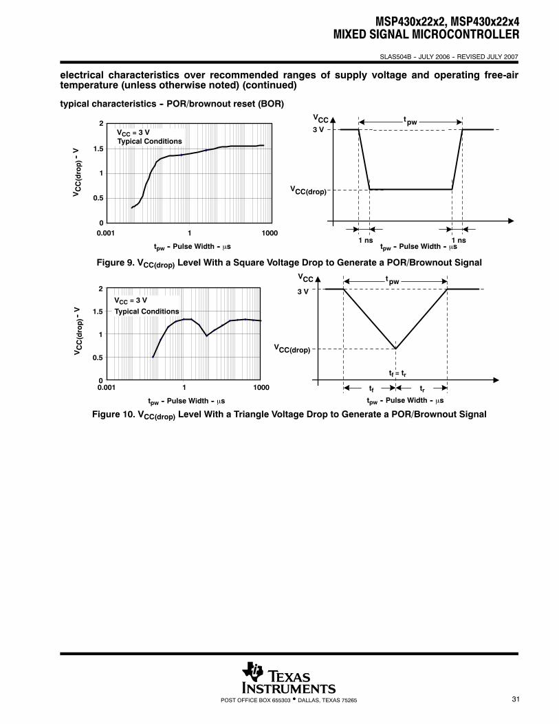
typical characteristics -- POR/brownout reset (BOR)
VCC(drop)
VCC3 V
tpw
0
0.5
1
1.5
2
0.001 1 1000
Typical Conditions
1 ns 1 nstpw -- Pulse Width -- μs
VCC(drop)--V
tpw -- Pulse Width -- μs
VCC = 3 V
Figure 9. VCC(drop) Level With a Square Voltage Drop to Generate a POR/Brownout SignalVCC
0
0.5
1
1.5
2
VCC(drop)
tpw
tpw -- Pulse Width -- μs
VCC(drop)--
V
3 V
0.001 1 1000 tf trtpw -- Pulse Width -- μs
tf = tr
Typical Conditions
VCC = 3 V
Figure 10. VCC(drop) Level With a Triangle Voltage Drop to Generate a POR/Brownout Signal
MSP430x22x2, MSP430x22x4MIXED SIGNAL MICROCONTROLLER
SLAS504B -- JULY 2006 -- REVISED JULY 2007
32 POST OFFICE BOX 655303 • DALLAS, TEXAS 75265
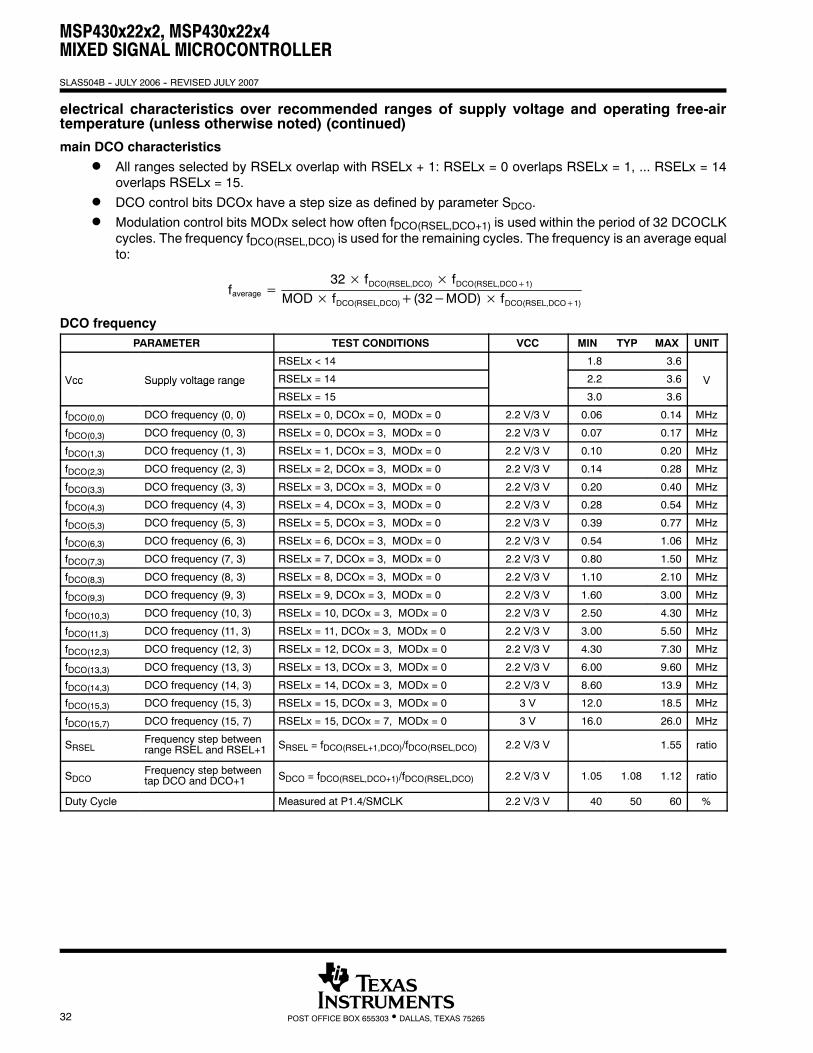
electrical characteristics over recommended ranges of supply voltage and operating free-airtemperature (unless otherwise noted) (continued)
main DCO characteristicsD All ranges selected by RSELx overlap with RSELx + 1: RSELx = 0 overlaps RSELx = 1, ... RSELx = 14
overlaps RSELx = 15.D DCO control bits DCOx have a step size as defined by parameter SDCO.D Modulation control bits MODx select how often fDCO(RSEL,DCO+1) is used within the period of 32 DCOCLK
cycles. The frequency fDCO(RSEL,DCO) is used for the remaining cycles. The frequency is an average equalto:
faverage=32× fDCO(RSEL,DCO)× fDCO(RSEL,DCO+1)
MOD× fDCO(RSEL,DCO)+(32−MOD)× fDCO(RSEL,DCO+1)
DCO frequencyPARAMETER TEST CONDITIONS VCC MIN TYP MAX UNIT
RSELx < 14 1.8 3.6
Vcc Supply voltage range RSELx = 14 2.2 3.6 VVcc Supply voltage range
RSELx = 15 3.0 3.6
V
fDCO(0,0) DCO frequency (0, 0) RSELx = 0, DCOx = 0, MODx = 0 2.2 V/3 V 0.06 0.14 MHz
fDCO(0,3) DCO frequency (0, 3) RSELx = 0, DCOx = 3, MODx = 0 2.2 V/3 V 0.07 0.17 MHz
fDCO(1,3) DCO frequency (1, 3) RSELx = 1, DCOx = 3, MODx = 0 2.2 V/3 V 0.10 0.20 MHz
fDCO(2,3) DCO frequency (2, 3) RSELx = 2, DCOx = 3, MODx = 0 2.2 V/3 V 0.14 0.28 MHz
fDCO(3,3) DCO frequency (3, 3) RSELx = 3, DCOx = 3, MODx = 0 2.2 V/3 V 0.20 0.40 MHz
fDCO(4,3) DCO frequency (4, 3) RSELx = 4, DCOx = 3, MODx = 0 2.2 V/3 V 0.28 0.54 MHz
fDCO(5,3) DCO frequency (5, 3) RSELx = 5, DCOx = 3, MODx = 0 2.2 V/3 V 0.39 0.77 MHz
fDCO(6,3) DCO frequency (6, 3) RSELx = 6, DCOx = 3, MODx = 0 2.2 V/3 V 0.54 1.06 MHz
fDCO(7,3) DCO frequency (7, 3) RSELx = 7, DCOx = 3, MODx = 0 2.2 V/3 V 0.80 1.50 MHz
fDCO(8,3) DCO frequency (8, 3) RSELx = 8, DCOx = 3, MODx = 0 2.2 V/3 V 1.10 2.10 MHz
fDCO(9,3) DCO frequency (9, 3) RSELx = 9, DCOx = 3, MODx = 0 2.2 V/3 V 1.60 3.00 MHz
fDCO(10,3) DCO frequency (10, 3) RSELx = 10, DCOx = 3, MODx = 0 2.2 V/3 V 2.50 4.30 MHz
fDCO(11,3) DCO frequency (11, 3) RSELx = 11, DCOx = 3, MODx = 0 2.2 V/3 V 3.00 5.50 MHz
fDCO(12,3) DCO frequency (12, 3) RSELx = 12, DCOx = 3, MODx = 0 2.2 V/3 V 4.30 7.30 MHz
fDCO(13,3) DCO frequency (13, 3) RSELx = 13, DCOx = 3, MODx = 0 2.2 V/3 V 6.00 9.60 MHz
fDCO(14,3) DCO frequency (14, 3) RSELx = 14, DCOx = 3, MODx = 0 2.2 V/3 V 8.60 13.9 MHz
fDCO(15,3) DCO frequency (15, 3) RSELx = 15, DCOx = 3, MODx = 0 3 V 12.0 18.5 MHz
fDCO(15,7) DCO frequency (15, 7) RSELx = 15, DCOx = 7, MODx = 0 3 V 16.0 26.0 MHz
SRSELFrequency step betweenrange RSEL and RSEL+1 SRSEL = fDCO(RSEL+1,DCO)/fDCO(RSEL,DCO) 2.2 V/3 V 1.55 ratio
SDCOFrequency step betweentap DCO and DCO+1 SDCO = fDCO(RSEL,DCO+1)/fDCO(RSEL,DCO) 2.2 V/3 V 1.05 1.08 1.12 ratio
Duty Cycle Measured at P1.4/SMCLK 2.2 V/3 V 40 50 60 %
MSP430x22x2, MSP430x22x4MIXED SIGNAL MICROCONTROLLER
SLAS504B -- JULY 2006 -- REVISED JULY 2007
33POST OFFICE BOX 655303 • DALLAS, TEXAS 75265
electrical characteristics over recommended ranges of supply voltage and operating free-airtemperature (unless otherwise noted) (continued)
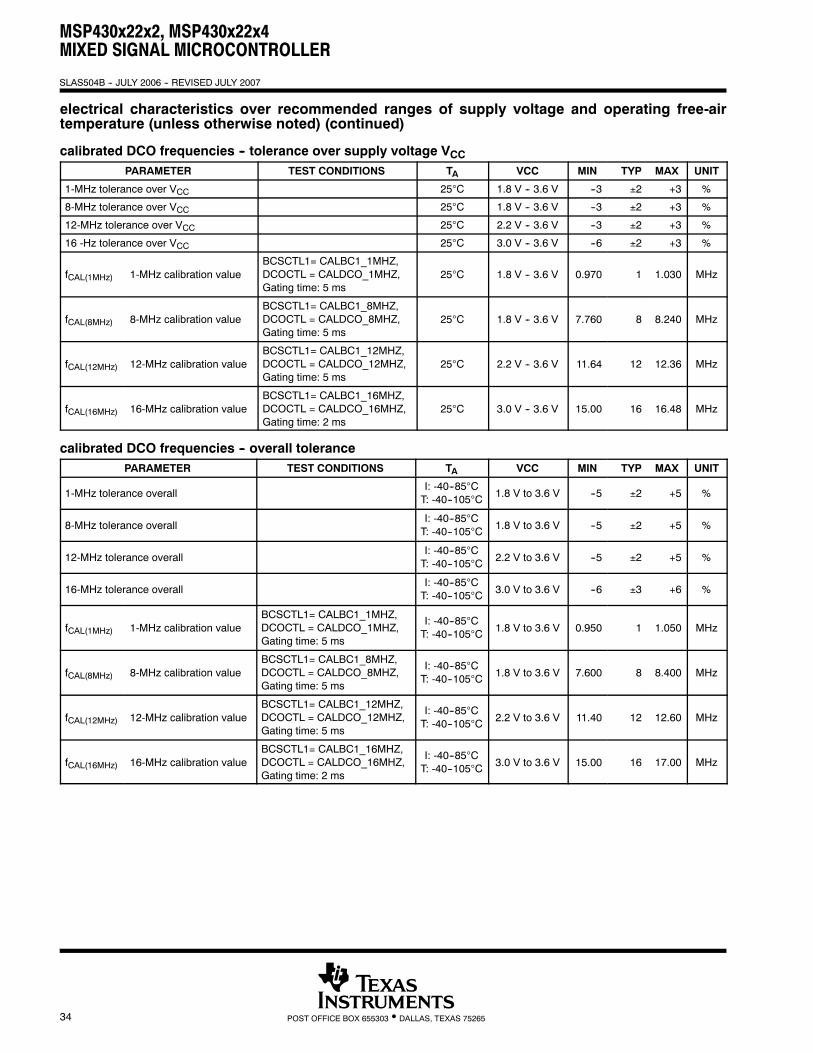
calibrated DCO frequencies -- tolerance at calibrationPARAMETER TEST CONDITIONS TA VCC MIN TYP MAX UNIT
Frequency tolerance at calibration 25°C 3 V --1 ±0.2 +1 %
fCAL(1MHz) 1-MHz calibration valueBCSCTL1= CALBC1_1MHZ,DCOCTL = CALDCO_1MHZ,Gating time: 5 ms
25°C 3 V 0.990 1 1.010 MHz
fCAL(8MHz) 8-MHz calibration valueBCSCTL1= CALBC1_8MHZ,DCOCTL = CALDCO_8MHZ,Gating time: 5 ms
25°C 3 V 7.920 8 8.080 MHz
fCAL(12MHz) 12-MHz calibration valueBCSCTL1= CALBC1_12MHZ,DCOCTL = CALDCO_12MHZ,Gating time: 5 ms
25°C 3 V 11.88 12 12.12 MHz
fCAL(16MHz) 16-MHz calibration valueBCSCTL1= CALBC1_16MHZ,DCOCTL = CALDCO_16MHZ,Gating time: 2 ms
25°C 3 V 15.84 16 16.16 MHz
calibrated DCO frequencies -- tolerance over temperature 0°C to +85°CPARAMETER TEST CONDITIONS TA VCC MIN TYP MAX UNIT
1-MHz tolerance over temperature 0--85°C 3.0 V --2.5 ±0.5 +2.5 %
8-MHz tolerance over temperature 0--85°C 3.0 V --2.5 ±1.0 +2.5 %
12-MHz tolerance over temperature 0--85°C 3.0 V --2.5 ±1.0 +2.5 %
16-MHz tolerance over temperature 0--85°C 3.0 V --3.0 ±2.0 +3.0 %
BCSCTL1= CALBC1 1MHZ, 2.2 V 0.970 1 1.030
fCAL(1MHz) 1-MHz calibration valueBCSCTL1= CALBC1_1MHZ,DCOCTL = CALDCO_1MHZ, 0--85°C 3.0 V 0.975 1 1.025 MHzfCAL(1MHz) 1 MHz calibration value DCOCTL CALDCO_1MHZ,Gating time: 5 ms
0 85 C
3.6 V 0.970 1 1.030
MHz
BCSCTL1= CALBC1 8MHZ, 2.2 V 7.760 8 8.400
fCAL(8MHz) 8-MHz calibration valueBCSCTL1= CALBC1_8MHZ,DCOCTL = CALDCO_8MHZ, 0--85°C 3.0 V 7.800 8 8.200 MHzfCAL(8MHz) 8 MHz calibration value DCOCTL CALDCO_8MHZ,Gating time: 5 ms
0 85 C
3.6 V 7.600 8 8.240
MHz
BCSCTL1= CALBC1 12MHZ, 2.2 V 11.70 12 12.30
fCAL(12MHz) 12-MHz calibration valueBCSCTL1= CALBC1_12MHZ,DCOCTL = CALDCO_12MHZ, 0--85°C 3.0 V 11.70 12 12.30 MHzfCAL(12MHz) 12 MHz calibration value DCOCTL CALDCO_12MHZ,Gating time: 5 ms
0 85 C
3.6 V 11.70 12 12.30
MHz
f 16 MHz calibration valueBCSCTL1= CALBC1_16MHZ,DCOCTL CALDCO 16MHZ 0 85°C
3.0 V 15.52 16 16.48MHzfCAL(16MHz) 16-MHz calibration value DCOCTL = CALDCO_16MHZ,
Gating time: 2 ms0--85°C
3.6 V 15.00 16 16.48MHz
MSP430x22x2, MSP430x22x4MIXED SIGNAL MICROCONTROLLER
SLAS504B -- JULY 2006 -- REVISED JULY 2007
34 POST OFFICE BOX 655303 • DALLAS, TEXAS 75265
electrical characteristics over recommended ranges of supply voltage and operating free-airtemperature (unless otherwise noted) (continued)
calibrated DCO frequencies -- tolerance over supply voltage VCCPARAMETER TEST CONDITIONS TA VCC MIN TYP MAX UNIT
1-MHz tolerance over VCC 25°C 1.8 V -- 3.6 V --3 ±2 +3 %
8-MHz tolerance over VCC 25°C 1.8 V -- 3.6 V --3 ±2 +3 %
12-MHz tolerance over VCC 25°C 2.2 V -- 3.6 V --3 ±2 +3 %
16 -Hz tolerance over VCC 25°C 3.0 V -- 3.6 V --6 ±2 +3 %
fCAL(1MHz) 1-MHz calibration valueBCSCTL1= CALBC1_1MHZ,DCOCTL = CALDCO_1MHZ,Gating time: 5 ms
25°C 1.8 V -- 3.6 V 0.970 1 1.030 MHz
fCAL(8MHz) 8-MHz calibration valueBCSCTL1= CALBC1_8MHZ,DCOCTL = CALDCO_8MHZ,Gating time: 5 ms
25°C 1.8 V -- 3.6 V 7.760 8 8.240 MHz
fCAL(12MHz) 12-MHz calibration valueBCSCTL1= CALBC1_12MHZ,DCOCTL = CALDCO_12MHZ,Gating time: 5 ms
25°C 2.2 V -- 3.6 V 11.64 12 12.36 MHz
fCAL(16MHz) 16-MHz calibration valueBCSCTL1= CALBC1_16MHZ,DCOCTL = CALDCO_16MHZ,Gating time: 2 ms
25°C 3.0 V -- 3.6 V 15.00 16 16.48 MHz
calibrated DCO frequencies -- overall tolerancePARAMETER TEST CONDITIONS TA VCC MIN TYP MAX UNIT
1-MHz tolerance overallI: -40--85°CT: -40--105°C 1.8 V to 3.6 V --5 ±2 +5 %
8-MHz tolerance overallI: -40--85°CT: -40--105°C 1.8 V to 3.6 V --5 ±2 +5 %
12-MHz tolerance overallI: -40--85°CT: -40--105°C 2.2 V to 3.6 V --5 ±2 +5 %
16-MHz tolerance overallI: -40--85°CT: -40--105°C 3.0 V to 3.6 V --6 ±3 +6 %
fCAL(1MHz) 1-MHz calibration valueBCSCTL1= CALBC1_1MHZ,DCOCTL = CALDCO_1MHZ,Gating time: 5 ms
I: -40--85°CT: -40--105°C 1.8 V to 3.6 V 0.950 1 1.050 MHz
fCAL(8MHz) 8-MHz calibration valueBCSCTL1= CALBC1_8MHZ,DCOCTL = CALDCO_8MHZ,Gating time: 5 ms
I: -40--85°CT: -40--105°C 1.8 V to 3.6 V 7.600 8 8.400 MHz
fCAL(12MHz) 12-MHz calibration valueBCSCTL1= CALBC1_12MHZ,DCOCTL = CALDCO_12MHZ,Gating time: 5 ms
I: -40--85°CT: -40--105°C 2.2 V to 3.6 V 11.40 12 12.60 MHz
fCAL(16MHz) 16-MHz calibration valueBCSCTL1= CALBC1_16MHZ,DCOCTL = CALDCO_16MHZ,Gating time: 2 ms
I: -40--85°CT: -40--105°C 3.0 V to 3.6 V 15.00 16 17.00 MHz
MSP430x22x2, MSP430x22x4MIXED SIGNAL MICROCONTROLLER
SLAS504B -- JULY 2006 -- REVISED JULY 2007
35POST OFFICE BOX 655303 • DALLAS, TEXAS 75265
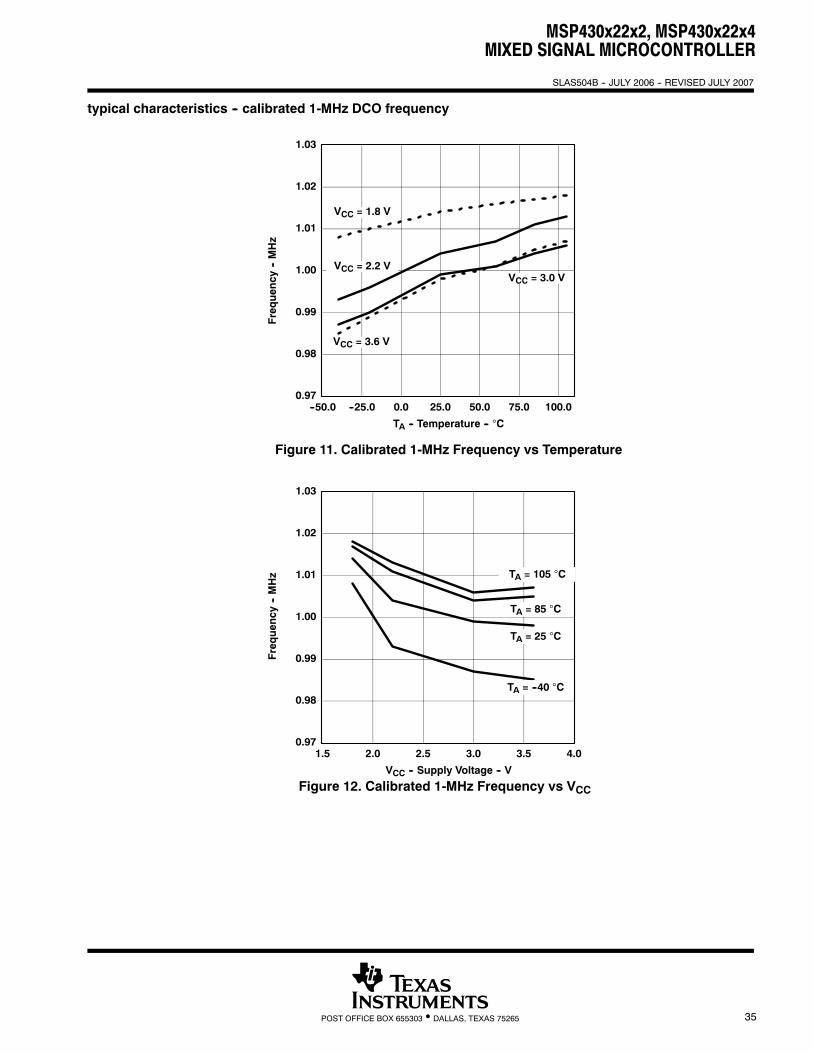
typical characteristics -- calibrated 1-MHz DCO frequency
TA -- Temperature -- °C
0.97
0.98
0.99
1.00
1.01
1.02
1.03
--50.0 --25.0 0.0 25.0 50.0 75.0 100.0
Frequency
--MHz
Figure 11. Calibrated 1-MHz Frequency vs Temperature
VCC = 1.8 V
VCC = 2.2 VVCC = 3.0 V
VCC = 3.6 V
VCC -- Supply Voltage -- V
0.97
0.98
0.99
1.00
1.01
1.02
1.03
1.5 2.0 2.5 3.0 3.5 4.0
Frequency
--MHz
Figure 12. Calibrated 1-MHz Frequency vs VCC
TA = --40 °C
TA = 25 °C
TA = 85 °C
TA = 105 °C
MSP430x22x2, MSP430x22x4MIXED SIGNAL MICROCONTROLLER
SLAS504B -- JULY 2006 -- REVISED JULY 2007
36 POST OFFICE BOX 655303 • DALLAS, TEXAS 75265
electrical characteristics over recommended ranges of supply voltage and operating free-airtemperature (unless otherwise noted) (continued)
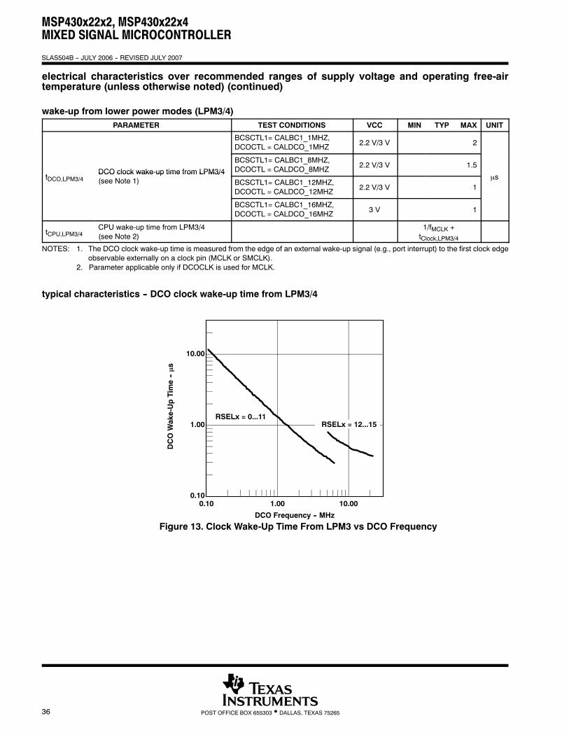
wake-up from lower power modes (LPM3/4)PARAMETER TEST CONDITIONS VCC MIN TYP MAX UNIT
BCSCTL1= CALBC1_1MHZ,DCOCTL = CALDCO_1MHZ 2.2 V/3 V 2
tDCO clock wake-up time from LPM3/4
BCSCTL1= CALBC1_8MHZ,DCOCTL = CALDCO_8MHZ 2.2 V/3 V 1.5
stDCO,LPM3/4DCO clock wake up time from LPM3/4(see Note 1) BCSCTL1= CALBC1_12MHZ,
DCOCTL = CALDCO_12MHZ 2.2 V/3 V 1μs
BCSCTL1= CALBC1_16MHZ,DCOCTL = CALDCO_16MHZ 3 V 1
tCPU,LPM3/4CPU wake-up time from LPM3/4(see Note 2)
1/fMCLK +tClock,LPM3/4
NOTES: 1. The DCO clock wake-up time is measured from the edge of an external wake-up signal (e.g., port interrupt) to the first clock edgeobservable externally on a clock pin (MCLK or SMCLK).
2. Parameter applicable only if DCOCLK is used for MCLK.
typical characteristics -- DCO clock wake-up time from LPM3/4
DCO Frequency -- MHz
0.10
1.00
10.00
0.10 1.00 10.00
Figure 13. Clock Wake-Up Time From LPM3 vs DCO Frequency
RSELx = 0...11RSELx = 12...15
DCOWake-UpTime--μs
MSP430x22x2, MSP430x22x4MIXED SIGNAL MICROCONTROLLER
SLAS504B -- JULY 2006 -- REVISED JULY 2007
37POST OFFICE BOX 655303 • DALLAS, TEXAS 75265
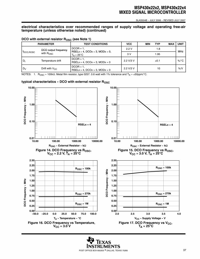
electrical characteristics over recommended ranges of supply voltage and operating free-airtemperature (unless otherwise noted) (continued)
DCO with external resistor ROSC (see Note 1)PARAMETER TEST CONDITIONS VCC MIN TYP MAX UNIT
f DCO output frequency DCOR = 1,RSELx 4 DCOx 3 MODx 0
2.2 V 1.8MHzfDCO,ROSC
DCO output frequencywith ROSC
RSELx = 4, DCOx = 3, MODx = 0,TA = 25°C 3 V 1.95
MHz
Dt Temperature driftDCOR = 1,RSELx = 4, DCOx = 3, MODx = 0 2.2 V/3 V ±0.1 %/°C
DV Drift with VCCDCOR = 1,RSELx = 4, DCOx = 3, MODx = 0 2.2 V/3 V 10 %/V
NOTES: 1. ROSC = 100kΩ. Metal film resistor, type 0257. 0.6 watt with 1% tolerance and TK = ±50ppm/°C.
typical characteristics -- DCO with external resistor ROSC
0.01
0.10
1.00
10.00
10.00 100.00 1000.00 10000.00
ROSC -- External Resistor -- kΩ
DCOFrequency
--MHz
Figure 14. DCO Frequency vs ROSC,VCC = 2.2 V, TA = 25°C
RSELx = 4
0.01
0.10
1.00
10.00
10.00 100.00 1000.00 10000.00
ROSC -- External Resistor -- kΩ
DCOFrequency
--MHz
Figure 15. DCO Frequency vs ROSC,VCC = 3.0 V, TA = 25°C
RSELx = 4
0.00
0.25
0.50
0.75
1.00
1.25
1.50
1.75
2.00
2.25
2.50
--50.0 --25.0 0.0 25.0 50.0 75.0 100.0
TA -- Temperature -- °C
DCOFrequency
--MHz
Figure 16. DCO Frequency vs Temperature,VCC = 3.0 V
ROSC = 100k
ROSC = 270k
ROSC = 1M
0.00
0.25
0.50
0.75
1.00
1.25
1.50
1.75
2.00
2.25
2.50
2.0 2.5 3.0 3.5 4.0
VCC -- Supply Voltage -- V
DCOFrequency
--MHz
Figure 17. DCO Frequency vs VCC,TA = 25°C
ROSC = 100k
ROSC = 270k
ROSC = 1M
MSP430x22x2, MSP430x22x4MIXED SIGNAL MICROCONTROLLER
SLAS504B -- JULY 2006 -- REVISED JULY 2007
38 POST OFFICE BOX 655303 • DALLAS, TEXAS 75265
electrical characteristics over recommended ranges of supply voltage and operating free-airtemperature (unless otherwise noted) (continued)
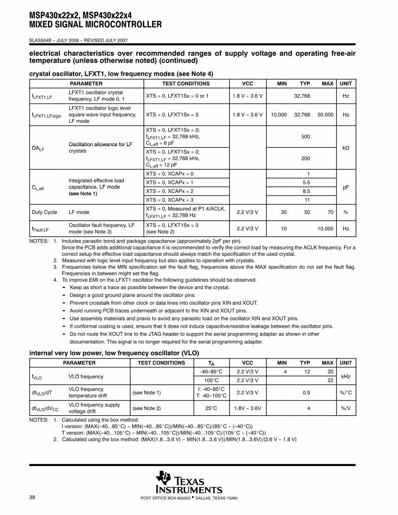
crystal oscillator, LFXT1, low frequency modes (see Note 4)PARAMETER TEST CONDITIONS VCC MIN TYP MAX UNIT
fLFXT1,LFLFXT1 oscillator crystalfrequency, LF mode 0, 1 XTS = 0, LFXT1Sx = 0 or 1 1.8 V -- 3.6 V 32,768 Hz
fLFXT1,LF,logicLFXT1 oscillator logic levelsquare wave input frequency,LF mode
XTS = 0, LFXT1Sx = 3 1.8 V -- 3.6 V 10,000 32,768 50,000 Hz
OAOscillation allowance for LF
XTS = 0, LFXT1Sx = 0;fLFXT1,LF = 32,768 kHz,CL,eff = 6 pF
500
kΩOALFOscillation allowance for LFcrystals XTS = 0, LFXT1Sx = 0;
fLFXT1,LF = 32,768 kHz,CL,eff = 12 pF
200
kΩ
XTS = 0, XCAPx = 0 1
CIntegrated effective loadcapacitance LF mode
XTS = 0, XCAPx = 1 5.5pFCL,eff capacitance, LF mode
(see Note 1) XTS = 0, XCAPx = 2 8.5pF
(see Note 1)XTS = 0, XCAPx = 3 11
Duty Cycle LF modeXTS = 0, Measured at P1.4/ACLK,fLFXT1,LF = 32,768 Hz
2.2 V/3 V 30 50 70 %
fFault,LFOscillator fault frequency, LFmode (see Note 3)
XTS = 0, LFXT1Sx = 3(see Note 2) 2.2 V/3 V 10 10,000 Hz
NOTES: 1. Includes parasitic bond and package capacitance (approximately 2pF per pin).Since the PCB adds additional capacitance it is recommended to verify the correct load by measuring the ACLK frequency. For acorrect setup the effective load capacitance should always match the specification of the used crystal.
2. Measured with logic level input frequency but also applies to operation with crystals.3. Frequencies below the MIN specification set the fault flag, frequencies above the MAX specification do not set the fault flag.
Frequencies in between might set the flag.4. To improve EMI on the LFXT1 oscillator the following guidelines should be observed.
-- Keep as short a trace as possible between the device and the crystal.-- Design a good ground plane around the oscillator pins.-- Prevent crosstalk from other clock or data lines into oscillator pins XIN and XOUT.-- Avoid running PCB traces underneath or adjacent to the XIN and XOUT pins.-- Use assembly materials and praxis to avoid any parasitic load on the oscillator XIN and XOUT pins.-- If conformal coating is used, ensure that it does not induce capacitive/resistive leakage between the oscillator pins.-- Do not route the XOUT line to the JTAG header to support the serial programming adapter as shown in other
documentation. This signal is no longer required for the serial programming adapter.
internal very low power, low frequency oscillator (VLO)PARAMETER TEST CONDITIONS TA VCC MIN TYP MAX UNIT
f VLO frequency-40--85°C 2.2 V/3 V 4 12 20
kHzfVLO VLO frequency105°C 2.2 V/3 V 22
kHz
dfVLO/dTVLO frequencytemperature drift (see Note 1)
I: -40--85°CT: -40--105°C 2.2 V/3 V 0.5 %/°C
dfVLO/dVCCVLO frequency supplyvoltage drift (see Note 2) 25°C 1.8V -- 3.6V 4 %/V
NOTES: 1. Calculated using the box method:I version: (MAX(--40...85_C) -- MIN(--40...85_C))/MIN(--40...85_C)/(85_C -- (--40_C))T version: (MAX(--40...105_C) -- MIN(--40...105_C))/MIN(--40...105_C)/(105_C -- (--40_C))
2. Calculated using the box method: (MAX(1.8...3.6 V) -- MIN(1.8...3.6 V))/MIN(1.8...3.6V)/(3.6 V -- 1.8 V)
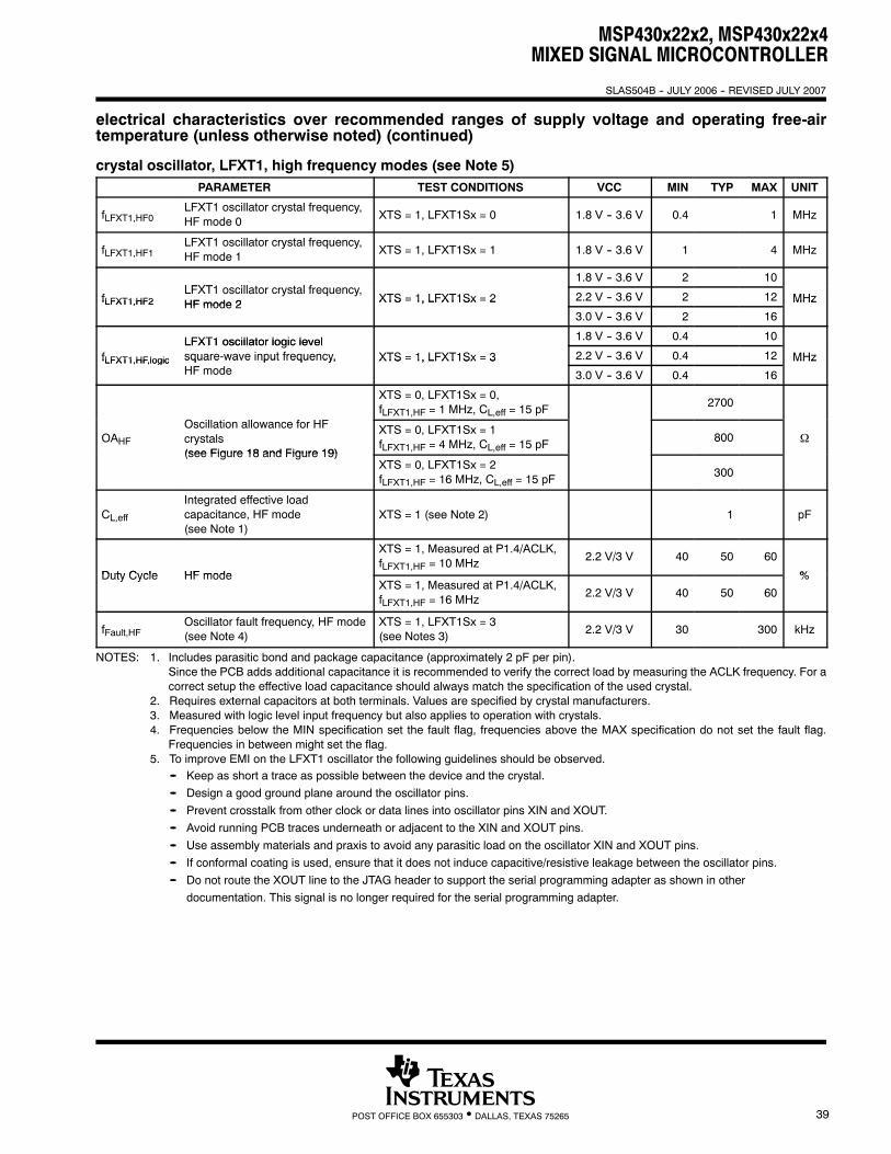
MSP430x22x2, MSP430x22x4MIXED SIGNAL MICROCONTROLLER
SLAS504B -- JULY 2006 -- REVISED JULY 2007
39POST OFFICE BOX 655303 • DALLAS, TEXAS 75265
electrical characteristics over recommended ranges of supply voltage and operating free-airtemperature (unless otherwise noted) (continued)
crystal oscillator, LFXT1, high frequency modes (see Note 5)PARAMETER TEST CONDITIONS VCC MIN TYP MAX UNIT
fLFXT1,HF0LFXT1 oscillator crystal frequency,HF mode 0 XTS = 1, LFXT1Sx = 0 1.8 V -- 3.6 V 0.4 1 MHz
fLFXT1,HF1LFXT1 oscillator crystal frequency,HF mode 1 XTS = 1, LFXT1Sx = 1 1.8 V -- 3.6 V 1 4 MHz
LFXT1 ill t t l f1.8 V -- 3.6 V 2 10
fLFXT1,HF2LFXT1 oscillator crystal frequency,HF mode 2 XTS = 1, LFXT1Sx = 2 2.2 V -- 3.6 V 2 12 MHzfLFXT1,HF2 HF mode 2 XTS 1, LFXT1Sx 2
3.0 V -- 3.6 V 2 16
MHz
LFXT1 oscillator logic level 1.8 V -- 3.6 V 0.4 10
fLFXT1,HF,logic
LFXT1 oscillator logic levelsquare-wave input frequency, XTS = 1, LFXT1Sx = 3 2.2 V -- 3.6 V 0.4 12 MHzfLFXT1,HF,logic square wave input frequency,HF mode
XTS 1, LFXT1Sx 3
3.0 V -- 3.6 V 0.4 16
MHz
XTS = 0, LFXT1Sx = 0,fLFXT1,HF = 1 MHz, CL,eff = 15 pF
2700
OAHFOscillation allowance for HFcrystals(see Figure 18 and Figure 19)
XTS = 0, LFXT1Sx = 1fLFXT1,HF = 4 MHz, CL,eff = 15 pF
800 Ω(see Figure 18 and Figure 19)
XTS = 0, LFXT1Sx = 2fLFXT1,HF = 16 MHz, CL,eff = 15 pF
300
CL,effIntegrated effective loadcapacitance, HF mode(see Note 1)
XTS = 1 (see Note 2) 1 pF
Duty Cycle HF mode
XTS = 1, Measured at P1.4/ACLK,fLFXT1,HF = 10 MHz
2.2 V/3 V 40 50 60
%Duty Cycle HF modeXTS = 1, Measured at P1.4/ACLK,fLFXT1,HF = 16 MHz
2.2 V/3 V 40 50 60%
fFault,HFOscillator fault frequency, HF mode(see Note 4)
XTS = 1, LFXT1Sx = 3(see Notes 3) 2.2 V/3 V 30 300 kHz
NOTES: 1. Includes parasitic bond and package capacitance (approximately 2 pF per pin).Since the PCB adds additional capacitance it is recommended to verify the correct load by measuring the ACLK frequency. For acorrect setup the effective load capacitance should always match the specification of the used crystal.
2. Requires external capacitors at both terminals. Values are specified by crystal manufacturers.3. Measured with logic level input frequency but also applies to operation with crystals.4. Frequencies below the MIN specification set the fault flag, frequencies above the MAX specification do not set the fault flag.
Frequencies in between might set the flag.5. To improve EMI on the LFXT1 oscillator the following guidelines should be observed.
-- Keep as short a trace as possible between the device and the crystal.-- Design a good ground plane around the oscillator pins.-- Prevent crosstalk from other clock or data lines into oscillator pins XIN and XOUT.-- Avoid running PCB traces underneath or adjacent to the XIN and XOUT pins.-- Use assembly materials and praxis to avoid any parasitic load on the oscillator XIN and XOUT pins.-- If conformal coating is used, ensure that it does not induce capacitive/resistive leakage between the oscillator pins.-- Do not route the XOUT line to the JTAG header to support the serial programming adapter as shown in other
documentation. This signal is no longer required for the serial programming adapter.
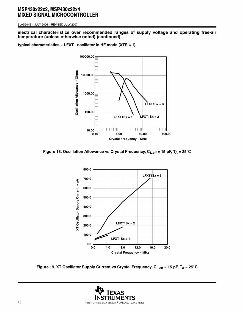
MSP430x22x2, MSP430x22x4MIXED SIGNAL MICROCONTROLLER
SLAS504B -- JULY 2006 -- REVISED JULY 2007
40 POST OFFICE BOX 655303 • DALLAS, TEXAS 75265
electrical characteristics over recommended ranges of supply voltage and operating free-airtemperature (unless otherwise noted) (continued)
typical characteristics -- LFXT1 oscillator in HF mode (XTS = 1)
Crystal Frequency -- MHz
10.00
100.00
1000.00
10000.00
100000.00
0.10 1.00 10.00 100.00
OscillationAllowance
--Ohms
LFXT1Sx = 1
LFXT1Sx = 3
LFXT1Sx = 2
Figure 18. Oscillation Allowance vs Crystal Frequency, CL,eff = 15 pF, TA = 25°C
0.0
100.0
200.0
300.0
400.0
500.0
600.0
700.0
800.0
0.0 4.0 8.0 12.0 16.0 20.0
Crystal Frequency -- MHz
XTOscillatorSupplyCurrent--uA
LFXT1Sx = 1
LFXT1Sx = 3
LFXT1Sx = 2
Figure 19. XT Oscillator Supply Current vs Crystal Frequency, CL,eff = 15 pF, TA = 25°C
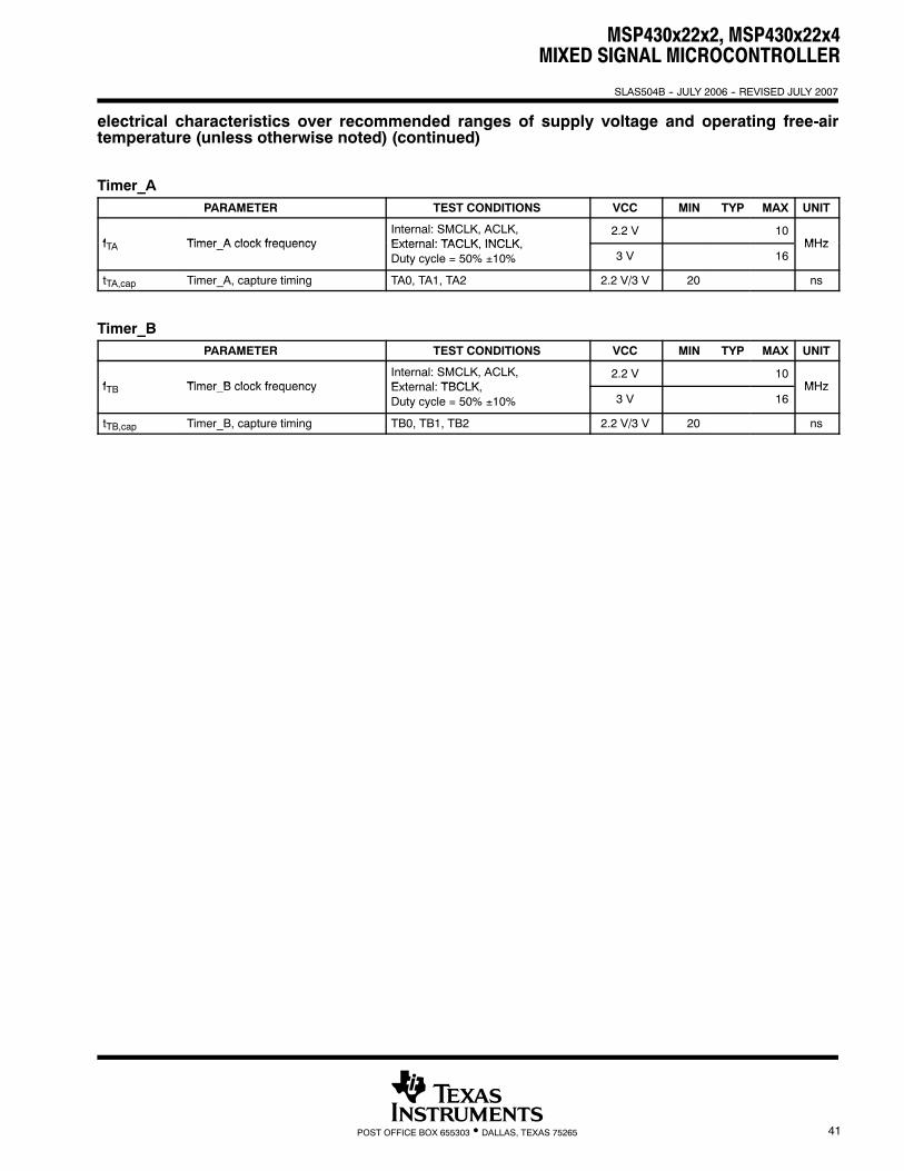
MSP430x22x2, MSP430x22x4MIXED SIGNAL MICROCONTROLLER
SLAS504B -- JULY 2006 -- REVISED JULY 2007
41POST OFFICE BOX 655303 • DALLAS, TEXAS 75265
electrical characteristics over recommended ranges of supply voltage and operating free-airtemperature (unless otherwise noted) (continued)
Timer_APARAMETER TEST CONDITIONS VCC MIN TYP MAX UNIT
f Timer A clock frequencyInternal: SMCLK, ACLK,External: TACLK INCLK
2.2 V 10MHzfTA Timer_A clock frequency External: TACLK, INCLK,
Duty cycle = 50% ±10% 3 V 16MHz
tTA,cap Timer_A, capture timing TA0, TA1, TA2 2.2 V/3 V 20 ns
Timer_BPARAMETER TEST CONDITIONS VCC MIN TYP MAX UNIT
f Timer B clock frequencyInternal: SMCLK, ACLK,External: TBCLK
2.2 V 10MHzfTB Timer_B clock frequency External: TBCLK,
Duty cycle = 50% ±10% 3 V 16MHz
tTB,cap Timer_B, capture timing TB0, TB1, TB2 2.2 V/3 V 20 ns
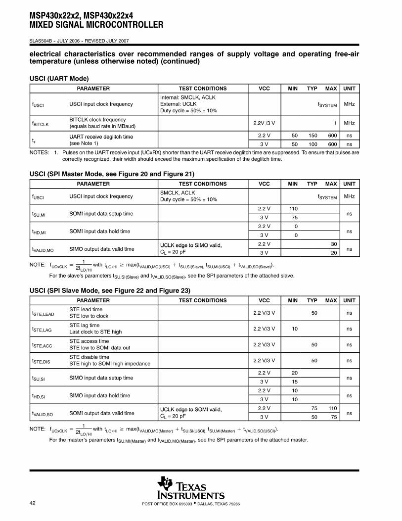
MSP430x22x2, MSP430x22x4MIXED SIGNAL MICROCONTROLLER
SLAS504B -- JULY 2006 -- REVISED JULY 2007
42 POST OFFICE BOX 655303 • DALLAS, TEXAS 75265
electrical characteristics over recommended ranges of supply voltage and operating free-airtemperature (unless otherwise noted) (continued)
USCI (UART Mode)PARAMETER TEST CONDITIONS VCC MIN TYP MAX UNIT
fUSCI USCI input clock frequencyInternal: SMCLK, ACLKExternal: UCLKDuty cycle = 50% ± 10%
fSYSTEM MHz
fBITCLKBITCLK clock frequency(equals baud rate in MBaud) 2.2V /3 V 1 MHz
tUART receive deglitch time 2.2 V 50 150 600 ns
tτUART receive deglitch time(see Note 1) 3 V 50 100 600 ns
NOTES: 1. Pulses on the UART receive input (UCxRX) shorter than the UART receive deglitch time are suppressed. To ensure that pulses arecorrectly recognized, their width should exceed the maximum specification of the deglitch time.
USCI (SPI Master Mode, see Figure 20 and Figure 21)PARAMETER TEST CONDITIONS VCC MIN TYP MAX UNIT
fUSCI USCI input clock frequencySMCLK, ACLKDuty cycle = 50% ± 10% fSYSTEM MHz
t SOMI input data setup time2.2 V 110
nstSU,MI SOMI input data setup time3 V 75
ns
t SOMI input data hold time2.2 V 0
nstHD,MI SOMI input data hold time3 V 0
ns
t SIMO output data valid timeUCLK edge to SIMO valid, 2.2 V 30
nstVALID,MO SIMO output data valid timeUCLK edge to SIMO valid,CL = 20 pF 3 V 20
ns
NOTE: fUCxCLK =1
2tLO∕HIwith tLO∕HI ≥ max(tVALID,MO(USCI)+ tSU,SI(Slave), tSU,MI(USCI)+ tVALID,SO(Slave)).
For the slave’s parameters tSU,SI(Slave) and tVALID,SO(Slave), see the SPI parameters of the attached slave.
USCI (SPI Slave Mode, see Figure 22 and Figure 23)PARAMETER TEST CONDITIONS VCC MIN TYP MAX UNIT
tSTE,LEADSTE lead timeSTE low to clock 2.2 V/3 V 50 ns
tSTE,LAGSTE lag timeLast clock to STE high 2.2 V/3 V 10 ns
tSTE,ACCSTE access timeSTE low to SOMI data out 2.2 V/3 V 50 ns
tSTE,DISSTE disable timeSTE high to SOMI high impedance 2.2 V/3 V 50 ns
t SIMO inp t data set p time2.2 V 20
nstSU,SI SIMO input data setup time3 V 15
ns
t SIMO inp t data hold time2.2 V 10
nstHD,SI SIMO input data hold time3 V 10
ns
t SOMI o tp t data alid timeUCLK edge to SOMI valid, 2.2 V 75 110
nstVALID,SO SOMI output data valid timeUCLK edge to SOMI valid,CL = 20 pF 3 V 50 75
ns
NOTE: fUCxCLK =1
2tLO∕HIwith tLO∕HI ≥ max(tVALID,MO(Master)+ tSU,SI(USCI), tSU,MI(Master)+ tVALID,SO(USCI)).
For the master’s parameters tSU,MI(Master) and tVALID,MO(Master), see the SPI parameters of the attached master.
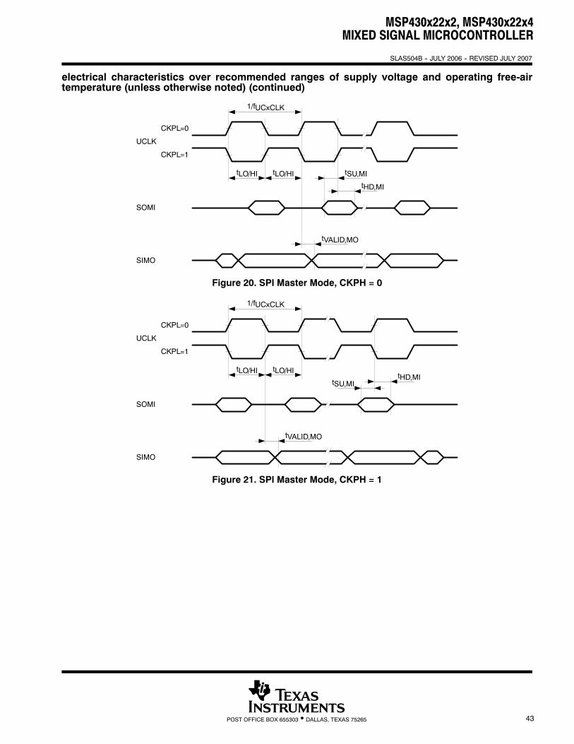
MSP430x22x2, MSP430x22x4MIXED SIGNAL MICROCONTROLLER
SLAS504B -- JULY 2006 -- REVISED JULY 2007
43POST OFFICE BOX 655303 • DALLAS, TEXAS 75265
electrical characteristics over recommended ranges of supply voltage and operating free-airtemperature (unless otherwise noted) (continued)
UCLK
CKPL=0
CKPL=1
SIMO
1/fUCxCLK
tLO/HI tLO/HI
SOMI
tSU,MI
tHD,MI
tVALID,MO
Figure 20. SPI Master Mode, CKPH = 0
UCLK
CKPL=0
CKPL=1
SIMO
1/fUCxCLK
tLO/HI tLO/HI
SOMI
tSU,MItHD,MI
tVALID,MO
Figure 21. SPI Master Mode, CKPH = 1
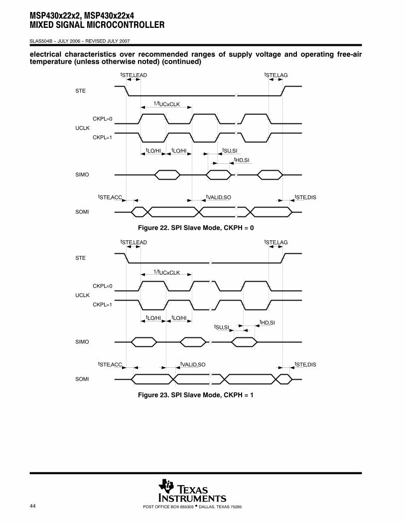
MSP430x22x2, MSP430x22x4MIXED SIGNAL MICROCONTROLLER
SLAS504B -- JULY 2006 -- REVISED JULY 2007
44 POST OFFICE BOX 655303 • DALLAS, TEXAS 75265
electrical characteristics over recommended ranges of supply voltage and operating free-airtemperature (unless otherwise noted) (continued)
STE
UCLK
CKPL=0
CKPL=1
SOMI
tSTE,ACC tSTE,DIS
1/fUCxCLK
tLO/HI tLO/HI
SIMO
tSU,SI
tHD,SI
tVALID,SO
tSTE,LEAD tSTE,LAG
Figure 22. SPI Slave Mode, CKPH = 0
STE
UCLK
CKPL=0
CKPL=1
tSTE,LEAD tSTE,LAG
tSTE,ACC tSTE,DIS
tLO/HI tLO/HI
tSU,SItHD,SI
tVALID,SO
SOMI
SIMO
1/fUCxCLK
Figure 23. SPI Slave Mode, CKPH = 1
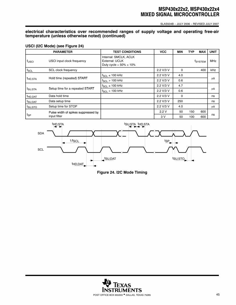
MSP430x22x2, MSP430x22x4MIXED SIGNAL MICROCONTROLLER
SLAS504B -- JULY 2006 -- REVISED JULY 2007
45POST OFFICE BOX 655303 • DALLAS, TEXAS 75265
electrical characteristics over recommended ranges of supply voltage and operating free-airtemperature (unless otherwise noted) (continued)
USCI (I2C Mode) (see Figure 24)PARAMETER TEST CONDITIONS VCC MIN TYP MAX UNIT
fUSCI USCI input clock frequencyInternal: SMCLK, ACLKExternal: UCLKDuty cycle = 50% ± 10%
fSYSTEM MHz
fSCL SCL clock frequency 2.2 V/3 V 0 400 kHz
t Hold time (repeated) STARTfSCL ≤ 100 kHz 2.2 V/3 V 4.0
stHD,STA Hold time (repeated) STARTfSCL > 100 kHz 2.2 V/3 V 0.6
μs
t Set p time for a repeated STARTfSCL ≤ 100 kHz 2.2 V/3 V 4.7
stSU,STA Setup time for a repeated STARTfSCL > 100 kHz 2.2 V/3 V 0.6
μs
tHD,DAT Data hold time 2.2 V/3 V 0 ns
tSU,DAT Data setup time 2.2 V/3 V 250 ns
tSU,STO Setup time for STOP 2.2 V/3 V 4.0 μs
tPulse width of spikes suppressed by 2.2 V 50 150 600
nstSPPulse width of spikes suppressed byinput filter 3 V 50 100 600
ns
SDA
SCL
1/fSCL
tHD,DAT
tSU,DAT
tHD,STA tSU,STA tHD,STA
tSU,STO
tSP
Figure 24. I2C Mode Timing
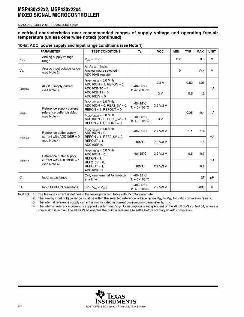
MSP430x22x2, MSP430x22x4MIXED SIGNAL MICROCONTROLLER
SLAS504B -- JULY 2006 -- REVISED JULY 2007
46 POST OFFICE BOX 655303 • DALLAS, TEXAS 75265
electrical characteristics over recommended ranges of supply voltage and operating free-airtemperature (unless otherwise noted) (continued)
10-bit ADC, power supply and input range conditions (see Note 1)PARAMETER TEST CONDITIONS TA VCC MIN TYP MAX UNIT
VCCAnalog supply voltagerange VSS = 0 V 2.2 3.6 V
VAxAnalog input voltage range(see Note 2)
All Ax terminals.Analog inputs selected inADC10AE register
0 VCC V
IADC10 supply current
fADC10CLK = 5.0 MHzADC10ON = 1, REFON = 0,ADC10SHT0 1
I: -40--85°C2.2 V 0.52 1.05
mAIADC10ADC10 supply current(see Note 3) ADC10SHT0 = 1,
ADC10SHT1 = 0,ADC10DIV = 0
I: 40 85 CT: -40--105°C
3 V 0.6 1.2
mA
IReference supply current,reference buffer disabled
fADC10CLK = 5.0 MHz,ADC10ON = 0, REF2_5V = 0,REFON = 1, REFOUT = 0
I: -40--85°CT: -40--105°C 2.2 V/3 V
0 25 0 4 mAIREF+ reference buffer disabled(see Note 4) fADC10CLK = 5.0 MHz,
ADC10ON = 0, REF2_5V = 1,REFON = 1, REFOUT = 0
I: -40--85°CT: -40--105°C 3 V
0.25 0.4 mA
IReference buffer supplycurrent with ADC10SR 0
fADC10CLK = 5.0 MHz,ADC10ON = 0,REFON 1 REF2 5V 0
-40--85°C 2.2 V/3 V 1.1 1.4
mAIREFB,0 current with ADC10SR = 0(see Note 4)
REFON = 1, REF2_5V = 0,REFOUT = 1,ADC10SR=0
105°C 2.2 V/3 V 1.8
mA
IReference buffer supplycurrent with ADC10SR 1
fADC10CLK = 5.0 MHz,ADC10ON = 0,REFON = 1,
-40--85°C 2.2 V/3 V 0.5 0.7
mAIREFB,1 current with ADC10SR = 1(see Note 4)
REFON = 1,REF2_5V = 0,REFOUT = 1,ADC10SR=1
105°C 2.2 V/3 V 0.8
mA
CI Input capacitanceOnly one terminal Ax selectedat a time
I: -40--85°CT: -40--105°C 27 pF
RI Input MUX ON resistance 0V ≤ VAx ≤ VCCI: -40--85°CT: -40--105°C 2.2 V/3 V 2000 Ω
NOTES: 1. The leakage current is defined in the leakage current table with Px.x/Ax parameter.2. The analog input voltage range must be within the selected reference voltage range VR+ to VR-- for valid conversion results.3. The internal reference supply current is not included in current consumption parameter IADC10.4. The internal reference current is supplied via terminal VCC. Consumption is independent of the ADC10ON control bit, unless a
conversion is active. The REFON bit enables the built-in reference to settle before starting an A/D conversion.
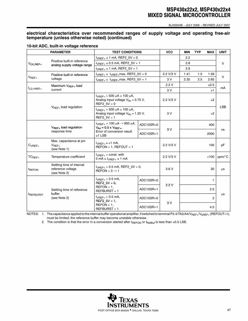
MSP430x22x2, MSP430x22x4MIXED SIGNAL MICROCONTROLLER
SLAS504B -- JULY 2006 -- REVISED JULY 2007
47POST OFFICE BOX 655303 • DALLAS, TEXAS 75265
electrical characteristics over recommended ranges of supply voltage and operating free-airtemperature (unless otherwise noted) (continued)
10-bit ADC, built-in voltage referencePARAMETER TEST CONDITIONS VCC MIN TYP MAX UNIT
P iti b ilt i fIVREF+ ≤ 1 mA, REF2_5V = 0 2.2
VCC,REF+Positive built-in referenceanalog supply voltage range
IVREF+ ≤ 0.5 mA, REF2_5V = 1 2.8 VVCC,REF+ analog supply voltage rangeIVREF+ ≤ 1 mA, REF2_5V = 1 2.9
V
VPositive built-in reference IVREF+ ≤ IVREF+max, REF2_5V = 0 2.2 V/3 V 1.41 1.5 1.59
VVREF+Positive built in referencevoltage IVREF+ ≤ IVREF+max, REF2_5V = 1 3 V 2.35 2.5 2.65
V
IMaximum VREF+ load 2.2 V ±0.5
mAILD,VREF+Maximum VREF+ loadcurrent 3 V ±1
mA
V load reg lation
IVREF+ = 500 μA ± 100 μA,Analog input voltage VAx ≈ 0.75 V,REF2_5V = 0
2.2 V/3 V ±2
LSBVREF+ load regulation IVREF+ = 500 μA ± 100 μA,Analog input voltage VAx ≈ 1.25 V,REF2_5V = 1
3 V ±2
LSB
VREF+ load regulationIVREF+ = 100 μA→ 900 μA,VAx ≈ 0.5 x VREF+,
ADC10SR=03 V
400ns
VREF+ load regulationresponse time
VAx ≈ 0.5 x VREF+,Error of conversion result≤1 LSB ADC10SR=1
3 V2000
ns
CVREF+Max. capacitance at pinVREF+(see Note 1)
IVREF+ ≤ ±1 mA,REFON = 1, REFOUT = 1 2.2 V/3 V 100 pF
TCREF+ Temperature coefficientIVREF+ = const. with0 mA ≤ IVREF+ ≤ 1 mA
2.2 V/3 V ±100 ppm/°C
tREFONSettling time of internalreference voltage(see Note 2)
IVREF+ = 0.5 mA, REF2_5V = 0,REFON = 0→ 1 3.6 V 30 μs
IVREF+ = 0.5 mA,REF2 5V = 0,
ADC10SR=02 2 V
1
tSettling time of referencebuffer
REF2_5V = 0,REFON = 1,REFBURST = 1 ADC10SR=1
2.2 V2.5
stREFBURST buffer(see Note 2) IVREF+ = 0.5 mA,
REF2 5V = 1,ADC10SR=0
3 V2
μs
REF2_5V = 1,REFON = 1,REFBURST = 1 ADC10SR=1
3 V4.5
NOTES: 1. Thecapacitanceapplied to the internal buffer operational amplifier, if switched to terminal P2.4/TA2/A4/VREF+/VeREF+ (REFOUT=1),must be limited; the reference buffer may become unstable otherwise.
2. The condition is that the error in a conversion started after tREFON or tRefBuf is less than ±0.5 LSB.
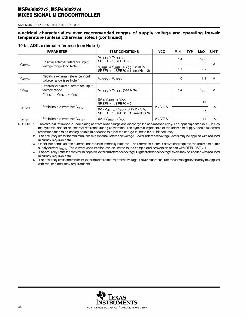
MSP430x22x2, MSP430x22x4MIXED SIGNAL MICROCONTROLLER
SLAS504B -- JULY 2006 -- REVISED JULY 2007
48 POST OFFICE BOX 655303 • DALLAS, TEXAS 75265
electrical characteristics over recommended ranges of supply voltage and operating free-airtemperature (unless otherwise noted) (continued)
10-bit ADC, external reference (see Note 1)PARAMETER TEST CONDITIONS VCC MIN TYP MAX UNIT
VPositive external reference input
VeREF+ > VeREF--,SREF1 = 1, SREF0 = 0 1.4 VCC
VVeREF+Positive external reference inputvoltage range (see Note 2) VeREF-- ≤ VeREF+ ≤ VCC -- 0.15 V,
SREF1 = 1, SREF0 = 1 (see Note 3) 1.4 3.0V
VeREF--Negative external reference inputvoltage range (see Note 4) VeREF+ > VeREF-- 0 1.2 V
∆VeREFDifferential external reference inputvoltage range∆VeREF = VeREF+ -- VeREF--
VeREF+ > VeREF-- (see Note 5) 1.4 VCC V
I Static input current into V
0V ≤ VeREF+ ≤ VCC,SREF1 = 1, SREF0 = 0
2 2 V/3 V
±1
AIVeREF+ Static input current into VeREF+ 0V ≤VeREF+ ≤ VCC -- 0.15 V ≤ 3 V,SREF1 = 1, SREF0 = 1 (see Note 3)
2.2 V/3 V0
μA
IVeREF-- Static input current into VeREF-- 0V ≤ VeREF-- ≤ VCC 2.2 V/3 V ±1 μA
NOTES: 1. The external reference is used during conversion to charge and discharge the capacitance array. The input capacitance, CI, is alsothe dynamic load for an external reference during conversion. The dynamic impedance of the reference supply should follow therecommendations on analog-source impedance to allow the charge to settle for 10-bit accuracy.
2. The accuracy limits the minimum positive external reference voltage. Lower reference voltage levels may be applied with reducedaccuracy requirements.
3. Under this condition, the external reference is internally buffered. The reference buffer is active and requires the reference buffersupply current IREFB. The current consumption can be limited to the sample and conversion period with REBURST = 1.
4. The accuracy limits themaximumnegative external reference voltage. Higher reference voltage levelsmay be appliedwith reducedaccuracy requirements.
5. The accuracy limits the minimum external differential reference voltage. Lower differential reference voltage levels may be appliedwith reduced accuracy requirements.
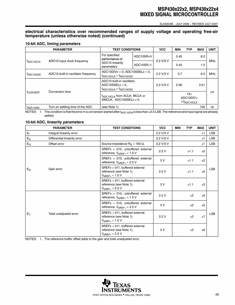
MSP430x22x2, MSP430x22x4MIXED SIGNAL MICROCONTROLLER
SLAS504B -- JULY 2006 -- REVISED JULY 2007
49POST OFFICE BOX 655303 • DALLAS, TEXAS 75265
electrical characteristics over recommended ranges of supply voltage and operating free-airtemperature (unless otherwise noted) (continued)
10-bit ADC, timing parametersPARAMETER TEST CONDITIONS VCC MIN TYP MAX UNIT
f ADC10 inp t clock freq enc
For specifiedperformance of
ADC10SR=02 2 V/3 V
0.45 6.3MHfADC10CLK ADC10 input clock frequency
performance ofADC10 linearityparameters ADC10SR=1
2.2 V/3 V0.45 1.5
MHz
fADC10OSC ADC10 built-in oscillator frequencyADC10DIVx = 0, ADC10SSELx = 0,fADC10CLK = fADC10OSC
2.2 V/3 V 3.7 6.3 MHz
t Con ersion time
ADC10 built-in oscillator,ADC10SSELx = 0,fADC10CLK = fADC10OSC
2.2 V/3 V 2.06 3.51
stCONVERT Conversion timefADC10CLK from ACLK, MCLK orSMCLK, ADC10SSELx ≠ 0
13×ADC10DIV×1/fADC10CLK
μs
tADC10ON Turn on settling time of the ADC (see Note 1) 100 ns
NOTES: 1. The condition is that the error in a conversion started after tADC10ON is less than ±0.5 LSB. The reference and input signal are alreadysettled.
10-bit ADC, linearity parametersPARAMETER TEST CONDITIONS VCC MIN TYP MAX UNIT
EI Integral linearity error 2.2 V/3 V ±1 LSB
ED Differential linearity error 2.2 V/3 V ±1 LSB
EO Offset error Source impedance RS < 100 Ω, 2.2 V/3 V ±1 LSB
SREFx = 010, unbuffered externalreference, VeREF+ = 1.5 V
2.2 V ±1.1 ±2
SREFx = 010, unbuffered externalreference, VeREF+ = 2.5 V
3 V ±1.1 ±2
EG Gain error SREFx = 011, buffered externalreference (see Note 1),VeREF+ = 1.5 V
2.2 V ±1.1 ±4LSB
SREFx = 011, buffered externalreference (see Note 1),VeREF+ = 2.5 V
3 V ±1.1 ±3
SREFx = 010, unbuffered externalreference, VeREF+ = 1.5 V
2.2 V ±2 ±5
SREFx = 010, unbuffered externalreference, VeREF+ = 2.5 V
3 V ±2 ±5
ET Total unadjusted error SREFx = 011, buffered externalreference (see Note 1),VeREF+ = 1.5 V
2.2 V ±2 ±7LSB
SREFx = 011, buffered externalreference (see Note 1),VeREF+ = 2.5 V
3 V ±2 ±6
NOTES: 1. The reference buffer offset adds to the gain and total unadjusted error.
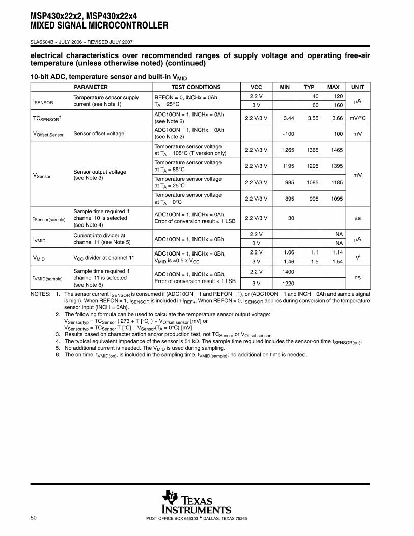
MSP430x22x2, MSP430x22x4MIXED SIGNAL MICROCONTROLLER
SLAS504B -- JULY 2006 -- REVISED JULY 2007
50 POST OFFICE BOX 655303 • DALLAS, TEXAS 75265
electrical characteristics over recommended ranges of supply voltage and operating free-airtemperature (unless otherwise noted) (continued)
10-bit ADC, temperature sensor and built-in VMIDPARAMETER TEST CONDITIONS VCC MIN TYP MAX UNIT
ITemperature sensor supply REFON = 0, INCHx = 0Ah, 2.2 V 40 120
AISENSORTemperature sensor supplycurrent (see Note 1)
REFON = 0, INCHx = 0Ah,TA = 25_C 3 V 60 160
μA
TCSENSOR†ADC10ON = 1, INCHx = 0Ah(see Note 2) 2.2 V/3 V 3.44 3.55 3.66 mV/°C
VOffset,Sensor Sensor offset voltageADC10ON = 1, INCHx = 0Ah(see Note 2) --100 100 mV
Temperature sensor voltageat TA = 105°C (T version only) 2.2 V/3 V 1265 1365 1465
V Sensor output voltage
Temperature sensor voltageat TA = 85°C
2.2 V/3 V 1195 1295 1395
mVVSensorSensor output voltage(see Note 3) Temperature sensor voltage
at TA = 25°C2.2 V/3 V 985 1085 1185
mV
Temperature sensor voltageat TA = 0°C
2.2 V/3 V 895 995 1095
tSensor(sample)Sample time required ifchannel 10 is selected(see Note 4)
ADC10ON = 1, INCHx = 0Ah,Error of conversion result ≤ 1 LSB 2.2 V/3 V 30 μs
ICurrent into divider at
ADC10ON 1 INCHx 0Bh2.2 V NA
AIVMIDCurrent into divider atchannel 11 (see Note 5) ADC10ON = 1, INCHx = 0Bh
3 V NAμA
V V divider at channel 11ADC10ON = 1, INCHx = 0Bh, 2.2 V 1.06 1.1 1.14
VVMID VCC divider at channel 11ADC10ON = 1, INCHx = 0Bh,VMID is ≈0.5 x VCC 3 V 1.46 1.5 1.54
V
tSample time required ifchannel 11 is selected
ADC10ON = 1, INCHx = 0Bh, 2.2 V 1400nstVMID(sample) channel 11 is selected
(see Note 6)
ADC10ON = 1, INCHx = 0Bh,Error of conversion result ≤ 1 LSB 3 V 1220
ns
NOTES: 1. The sensor current ISENSOR is consumed if (ADC10ON = 1 and REFON = 1), or (ADC10ON = 1 and INCH = 0Ah and sample signalis high). When REFON = 1, ISENSOR is included in IREF+. When REFON = 0, ISENSOR applies during conversion of the temperaturesensor input (INCH = 0Ah).
2. The following formula can be used to calculate the temperature sensor output voltage:VSensor,typ = TCSensor ( 273 + T [°C] ) + VOffset,sensor [mV] orVSensor,typ = TCSensor T [°C] + VSensor(TA = 0°C) [mV]
3. Results based on characterization and/or production test, not TCSensor or VOffset,sensor.4. The typical equivalent impedance of the sensor is 51 kΩ. The sample time required includes the sensor-on time tSENSOR(on).5. No additional current is needed. The VMID is used during sampling.6. The on time, tVMID(on), is included in the sampling time, tVMID(sample); no additional on time is needed.
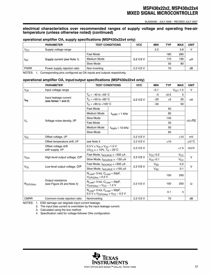
MSP430x22x2, MSP430x22x4MIXED SIGNAL MICROCONTROLLER
SLAS504B -- JULY 2006 -- REVISED JULY 2007
51POST OFFICE BOX 655303 • DALLAS, TEXAS 75265
electrical characteristics over recommended ranges of supply voltage and operating free-airtemperature (unless otherwise noted) (continued)
operational amplifier OA, supply specifications (MSP430x22x4 only)PARAMETER TEST CONDITIONS VCC MIN TYP MAX UNIT
VCC Supply voltage range 2.2 3.6 V
Fast Mode 180 290
ICC Supply current (see Note 1) Medium Mode 2.2 V/3 V 110 190 μAICC Supply current (see Note 1)
Slow Mode
2.2 V/3 V
50 80
μA
PSRR Power supply rejection ratio Non-inverting 2.2 V/3 V 70 dB
NOTES: 1. Corresponding pins configured as OA inputs and outputs respectively.
operational amplifier OA, input/output specifications (MSP430x22x4 only)PARAMETER TEST CONDITIONS VCC MIN TYP MAX UNIT
VI/P Input voltage range --0.1 VCC--1.2 V
I t l k tTA = --40 to +55_C --5 ±0.5 5
IIkgInput leakage current(see Notes 1 and 2)
TA = +55 to +85_C 2.2 V/3 V --20 ±5 20 nAIIkg (see Notes 1 and 2)TA = +85 to +105_C
2.2 V/3 V
--50 50
nA
Fast Mode 50
Medium Mode fV(I/P) = 1 kHz 80
V Voltage noise densit I/PSlow Mode
fV(I/P) 1 kHz
140nV/√HVn Voltage noise density, I/P
Fast Mode 30nV/√Hz
Medium Mode fV(I/P) = 10 kHz 50
Slow Mode
fV(I/P) 10 kHz
65
VIO Offset voltage, I/P 2.2 V/3 V ±10 mV
Offset temperature drift, I/P see Note 3 2.2 V/3 V ±10 μV/°C
Offset voltage driftwith supply, I/P
0.3 V ≤ VIN ≤ VCC--1.0 V∆VCC ≤ ± 10%, TA = 25°C
2.2 V/3 V ±1.5 mV/V
V High level output voltage O/PFast Mode, ISOURCE ≤ --500 μA
2 2 V/3 VVCC--0.2 VCC
VVOH High-level output voltage, O/PSlow Mode, ISOURCE ≤ --150 μA
2.2 V/3 VVCC--0.1 VCC
V
V Low level output voltage O/PFast Mode, ISOURCE ≤ +500 μA
2 2 V/3 VVSS 0.2
VVOL Low-level output voltage, O/PSlow Mode, ISOURCE ≤ +150 μA
2.2 V/3 VVSS 0.1
V
RLoad= 3 kΩ, CLoad = 50pF,VO/P(OAx) < 0.2 V
150 250
RO/P(OAx)Output resistance(see Figure 25 and Note 4)
RLoad= 3 kΩ, CLoad = 50pF,VO/P(OAx) > VCC -- 1.2 V 2.2 V/3 V 150 250 Ω
RLoad= 3 kΩ, CLoad = 50pF,0.2 V ≤ VO/P(OAx) ≤ VCC -- 0.2 V 0.1 4
CMRR Common-mode rejection ratio Noninverting 2.2 V/3 V 70 dB
NOTES: 1. ESD damage can degrade input current leakage.2. The input bias current is overridden by the input leakage current.3. Calculated using the box method4. Specification valid for voltage-follower OAx configuration
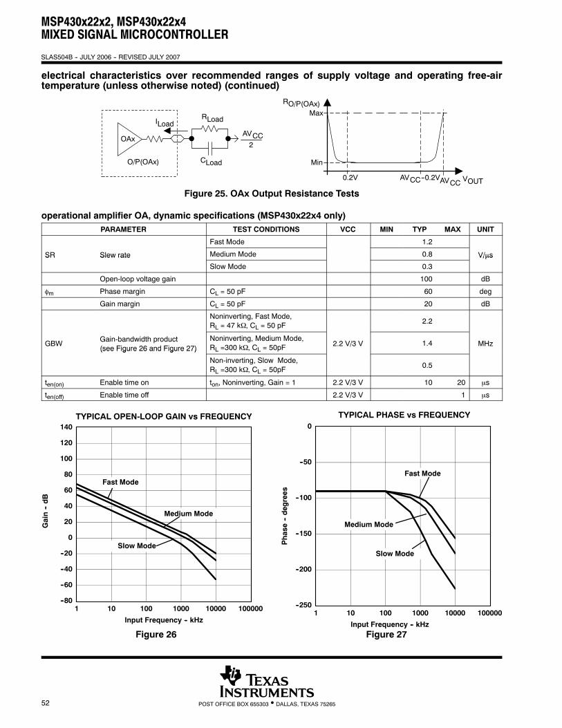
MSP430x22x2, MSP430x22x4MIXED SIGNAL MICROCONTROLLER
SLAS504B -- JULY 2006 -- REVISED JULY 2007
52 POST OFFICE BOX 655303 • DALLAS, TEXAS 75265
electrical characteristics over recommended ranges of supply voltage and operating free-airtemperature (unless otherwise noted) (continued)
RO/P(OAx)Max
0.2V AVCCAVCC--0.2V VOUT
Min
RLoad
AVCC
CLoad
2
ILoad
OAx
O/P(OAx)
Figure 25. OAx Output Resistance Tests
operational amplifier OA, dynamic specifications (MSP430x22x4 only)PARAMETER TEST CONDITIONS VCC MIN TYP MAX UNIT
Fast Mode 1.2
SR Slew rate Medium Mode 0.8 V/μsSR Slew rate
Slow Mode 0.3
V/μs
Open-loop voltage gain 100 dB
φm Phase margin CL = 50 pF 60 deg
Gain margin CL = 50 pF 20 dB
Noninverting, Fast Mode,RL = 47 kΩ, CL = 50 pF
2.2
GBW Gain-bandwidth product(see Figure 26 and Figure 27)
Noninverting, Medium Mode,RL =300 kΩ, CL = 50pF
2.2 V/3 V 1.4 MHz(see Figure 26 and Figure 27)
Non-inverting, Slow Mode,RL =300 kΩ, CL = 50pF
0.5
ten(on) Enable time on ton, Noninverting, Gain = 1 2.2 V/3 V 10 20 μs
ten(off) Enable time off 2.2 V/3 V 1 μs
Figure 26
Input Frequency -- kHz
--80
--60
--40
--20
0
20
40
60
80
100
120
140
1 10 100 1000 10000 100000
TYPICAL OPEN-LOOP GAIN vs FREQUENCY
Slow Mode
Fast Mode
Gain--dB
Medium Mode
Figure 27Input Frequency -- kHz
--250
--200
--150
--100
--50
0
1 10 100 1000 10000 100000
TYPICAL PHASE vs FREQUENCY
Phase--degrees
Slow Mode
Fast Mode
Medium Mode
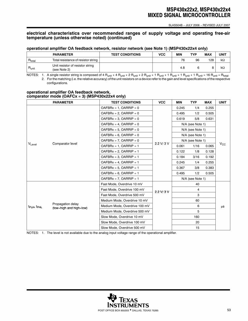
MSP430x22x2, MSP430x22x4MIXED SIGNAL MICROCONTROLLER
SLAS504B -- JULY 2006 -- REVISED JULY 2007
53POST OFFICE BOX 655303 • DALLAS, TEXAS 75265
electrical characteristics over recommended ranges of supply voltage and operating free-airtemperature (unless otherwise noted) (continued)
operational amplifier OA feedback network, resistor network (see Note 1) (MSP430x22x4 only)PARAMETER TEST CONDITIONS VCC MIN TYP MAX UNIT
Rtotal Total resistance of resistor string 76 96 128 kΩ
RunitUnit resistor of resistor string(see Note 2) 4.8 6 8 kΩ
NOTES: 1. A single resistor string is composed of 4 Runit + 4 Runit + 2 Runit + 2 Runit + 1 Runit + 1 Runit + 1 Runit + 1 Runit = 16 Runit = Rtotal.2. For thematching (i.e. the relative accuracy) of the unit resistors on a device refer to the gain and level specifications of the respective
configurations.
operational amplifier OA feedback network,comparator mode (OAFCx = 3) (MSP430x22x4 only)
PARAMETER TEST CONDITIONS VCC MIN TYP MAX UNIT
OAFBRx = 1, OARRIP = 0 0.245 1/4 0.255
OAFBRx = 2, OARRIP = 0 0.495 1/2 0.505
OAFBRx = 3, OARRIP = 0 0.619 5/8 0.631
OAFBRx = 4, OARRIP = 0 N/A (see Note 1)
OAFBRx = 5, OARRIP = 0 N/A (see Note 1)
OAFBRx = 6, OARRIP = 0 N/A (see Note 1)
V Comparator levelOAFBRx = 7, OARRIP = 0
2 2 V/ 3 VN/A (see Note 1)
VVLevel Comparator levelOAFBRx = 1, OARRIP = 1
2.2 V/ 3 V0.061 1/16 0.065
VCC
OAFBRx = 2, OARRIP = 1 0.122 1/8 0.128
OAFBRx = 3, OARRIP = 1 0.184 3/16 0.192
OAFBRx = 4, OARRIP = 1 0.245 1/4 0.255
OAFBRx = 5, OARRIP = 1 0.367 3/8 0.383
OAFBRx = 6, OARRIP = 1 0.495 1/2 0.505
OAFBRx = 7, OARRIP = 1 N/A (see Note 1)
Fast Mode, Overdrive 10 mV 40
Fast Mode, Overdrive 100 mV2 2 V/ 3 V
4
Fast Mode, Overdrive 500 mV2.2 V/ 3 V
3
P ti d lMedium Mode, Overdrive 10 mV 60
tPLH, tPHLPropagation delay(low--high and high--low)
Medium Mode, Overdrive 100 mV 6 μstPLH, tPHL (low--high and high--low)Medium Mode, Overdrive 500 mV 5
μs
Slow Mode, Overdrive 10 mV 160
Slow Mode, Overdrive 100 mV 20
Slow Mode, Overdrive 500 mV 15
NOTES: 1. The level is not available due to the analog input voltage range of the operational amplifier.
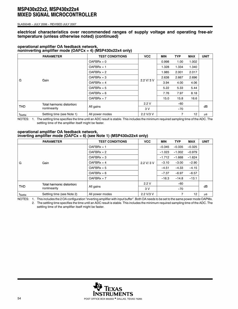
MSP430x22x2, MSP430x22x4MIXED SIGNAL MICROCONTROLLER
SLAS504B -- JULY 2006 -- REVISED JULY 2007
54 POST OFFICE BOX 655303 • DALLAS, TEXAS 75265
electrical characteristics over recommended ranges of supply voltage and operating free-airtemperature (unless otherwise noted) (continued)
operational amplifier OA feedback network,noninverting amplifier mode (OAFCx = 4) (MSP430x22x4 only)
PARAMETER TEST CONDITIONS VCC MIN TYP MAX UNIT
OAFBRx = 0 0.998 1.00 1.002
OAFBRx = 1 1.328 1.334 1.340
OAFBRx = 2 1.985 2.001 2.017
G GainOAFBRx = 3
2 2 V/ 3 V2.638 2.667 2.696
G GainOAFBRx = 4
2.2 V/ 3 V3.94 4.00 4.06
OAFBRx = 5 5.22 5.33 5.44
OAFBRx = 6 7.76 7.97 8.18
OAFBRx = 7 15.0 15.8 16.6
THDTotal harmonic distortion/
All gains2.2 V --60
dBTHDTotal harmonic distortion/nonlinearity All gains
3 V --70dB
tSettle Settling time (see Note 1) All power modes 2.2 V/3 V 7 12 μs
NOTES: 1. The settling time specifies the time until an ADC result is stable. This includes the minimum required sampling time of the ADC. Thesettling time of the amplifier itself might be faster.
operational amplifier OA feedback network,inverting amplifier mode (OAFCx = 6) (see Note 1) (MSP430x22x4 only)
PARAMETER TEST CONDITIONS VCC MIN TYP MAX UNIT
OAFBRx = 1 --0.345 --0.335 --0.325
OAFBRx = 2 --1.023 --1.002 --0.979
OAFBRx = 3 --1.712 --1.668 --1.624
G Gain OAFBRx = 4 2.2 V/ 3 V --3.10 --3.00 --2.90G Gain
OAFBRx = 5
2.2 V/ 3 V
--4.51 --4.33 --4.15
OAFBRx = 6 --7.37 --6.97 --6.57
OAFBRx = 7 --16.3 --14.8 --13.1
THDTotal harmonic distortion/
All gains2.2 V --60
dBTHDTotal harmonic distortion/nonlinearity All gains
3 V --70dB
tSettle Settling time (see Note 2) All power modes 2.2 V/3 V 7 12 μs
NOTES: 1. This includes the 2OAconfiguration “inverting amplifierwith input buffer”. BothOAneeds to be set to the samepowermodeOAPMx.2. The settling time specifies the time until an ADC result is stable. This includes the minimum required sampling time of the ADC. The
settling time of the amplifier itself might be faster.
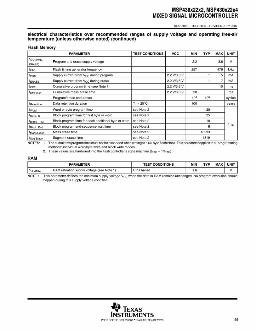
MSP430x22x2, MSP430x22x4MIXED SIGNAL MICROCONTROLLER
SLAS504B -- JULY 2006 -- REVISED JULY 2007
55POST OFFICE BOX 655303 • DALLAS, TEXAS 75265
electrical characteristics over recommended ranges of supply voltage and operating free-airtemperature (unless otherwise noted) (continued)
Flash MemoryPARAMETER TEST CONDITIONS VCC MIN TYP MAX UNIT
VCC(PGM/ERASE)
Program and erase supply voltage 2.2 3.6 V
fFTG Flash timing generator frequency 257 476 kHz
IPGM Supply current from VCC during program 2.2 V/3.6 V 1 5 mA
IERASE Supply current from VCC during erase 2.2 V/3.6 V 1 7 mA
tCPT Cumulative program time (see Note 1) 2.2 V/3.6 V 10 ms
tCMErase Cumulative mass erase time 2.2 V/3.6 V 20 ms
Program/erase endurance 104 105 cycles
tRetention Data retention duration TJ = 25°C 100 years
tWord Word or byte program time see Note 2 30
tBlock, 0 Block program time for first byte or word see Note 2 25
tBlock, 1-63 Block program time for each additional byte or word see Note 2 18t
tBlock, End Block program end-sequence wait time see Note 2 6tFTG
tMass Erase Mass erase time see Note 2 10593
tSeg Erase Segment erase time see Note 2 4819
NOTES: 1. The cumulative program timemust not be exceededwhenwriting to a 64-byte flash block. This parameter applies to all programmingmethods: individual word/byte write and block write modes.
2. These values are hardwired into the flash controller’s state machine (tFTG = 1/fFTG).
RAMPARAMETER TEST CONDITIONS MIN TYP MAX UNIT
V(RAMh) RAM retention supply voltage (see Note 1) CPU halted 1.6 V
NOTE 1: This parameter defines the minimum supply voltage VCC when the data in RAM remains unchanged. No program execution shouldhappen during this supply voltage condition.
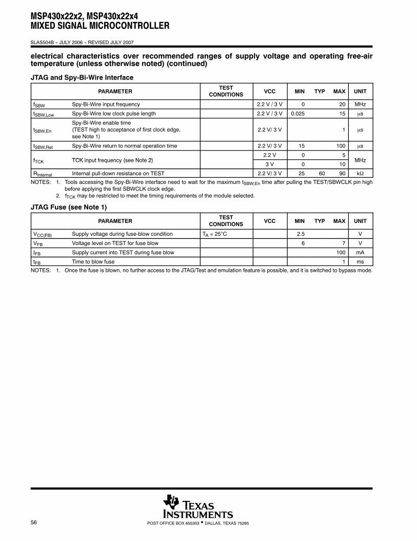
MSP430x22x2, MSP430x22x4MIXED SIGNAL MICROCONTROLLER
SLAS504B -- JULY 2006 -- REVISED JULY 2007
56 POST OFFICE BOX 655303 • DALLAS, TEXAS 75265
electrical characteristics over recommended ranges of supply voltage and operating free-airtemperature (unless otherwise noted) (continued)
JTAG and Spy-Bi-Wire Interface
PARAMETERTEST
CONDITIONS VCC MIN TYP MAX UNIT
fSBW Spy-Bi-Wire input frequency 2.2 V / 3 V 0 20 MHz
tSBW,Low Spy-Bi-Wire low clock pulse length 2.2 V / 3 V 0.025 15 μs
tSBW,EnSpy-Bi-Wire enable time(TEST high to acceptance of first clock edge,see Note 1)
2.2 V/ 3 V 1 μs
tSBW,Ret Spy-Bi-Wire return to normal operation time 2.2 V/ 3 V 15 100 μs
f TCK inp t freq enc (see Note 2)2.2 V 0 5
MHfTCK TCK input frequency (see Note 2)3 V 0 10
MHz
RInternal Internal pull-down resistance on TEST 2.2 V/ 3 V 25 60 90 kΩ
NOTES: 1. Tools accessing the Spy-Bi-Wire interface need to wait for the maximum tSBW,En time after pulling the TEST/SBWCLK pin highbefore applying the first SBWCLK clock edge.
2. fTCK may be restricted to meet the timing requirements of the module selected.
JTAG Fuse (see Note 1)
PARAMETERTEST
CONDITIONS VCC MIN TYP MAX UNIT
VCC(FB) Supply voltage during fuse-blow condition TA = 25°C 2.5 V
VFB Voltage level on TEST for fuse blow 6 7 V
IFB Supply current into TEST during fuse blow 100 mA
tFB Time to blow fuse 1 ms
NOTES: 1. Once the fuse is blown, no further access to the JTAG/Test and emulation feature is possible, and it is switched to bypass mode.
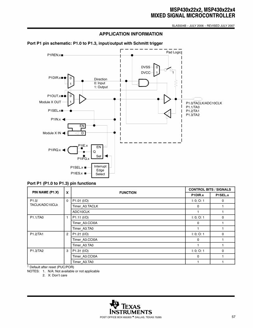
MSP430x22x2, MSP430x22x4MIXED SIGNAL MICROCONTROLLER
SLAS504B -- JULY 2006 -- REVISED JULY 2007
57POST OFFICE BOX 655303 • DALLAS, TEXAS 75265
APPLICATION INFORMATION
Port P1 pin schematic: P1.0 to P1.3, input/output with Schmitt trigger
Direction0: Input1: Output
P1SEL.x
1
0P1DIR.x
P1IN.x
P1IRQ.x
D
EN
Module X IN
1
0
Module X OUT
P1OUT.x
InterruptEdgeSelect
QEN
Set
P1SEL.x
P1IES.x
P1IFG.x
P1IE.x
P1.0/TACLK/ADC10CLKP1.1/TA0P1.2/TA1P1.3/TA2
1
0DVSS
DVCC
P1REN.xPad Logic
1
Port P1 (P1.0 to P1.3) pin functions
PIN NAME (P1 X) X FUNCTIONCONTROL BITS / SIGNALS
PIN NAME (P1.X) X FUNCTIONP1DIR.x P1SEL.x
P1.0/ 0 P1.0† (I/O) I: 0; O: 1 0/TACLK/ADC10CLk Timer_A3.TACLK 0 1
ADC10CLK 1 1
P1.1/TA0 1 P1.1† (I/O) I: 0; O: 1 0/
Timer_A3.CCI0A 0 1
Timer_A3.TA0 1 1
P1.2/TA1 2 P1.2† (I/O) I: 0; O: 1 0/
Timer_A3.CCI0A 0 1
Timer_A3.TA0 1 1
P1.3/TA2 3 P1.3† (I/O) I: 0; O: 1 0/
Timer_A3.CCI0A 0 1
Timer_A3.TA0 1 1† Default after reset (PUC/POR)NOTES: 1. N/A: Not available or not applicable
2. X: Don’t care
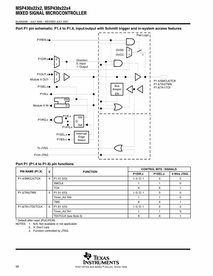
MSP430x22x2, MSP430x22x4MIXED SIGNAL MICROCONTROLLER
SLAS504B -- JULY 2006 -- REVISED JULY 2007
58 POST OFFICE BOX 655303 • DALLAS, TEXAS 75265
Port P1 pin schematic: P1.4 to P1.6, input/output with Schmitt trigger and in-system access features
BusKeeper
EN
Direction0: Input1: Output
P1SEL.x
1
0P1DIR.x
P1IN.x
P1IRQ.x
D
EN
Module X IN
1
0
Module X OUT
P1OUT.x
InterruptEdgeSelect
QEN
Set
P1SEL.x
P1IES.x
P1IFG.x
P1IE.x
P1.4/SMCLK/TCKP1.5/TA0/TMSP1.6/TA1/TDI
1
0DVSS
DVCC
P1REN.x
To JTAG
From JTAG
1
Pad Logic
Port P1 (P1.4 to P1.6) pin functions
PIN NAME (P1 X) X FUNCTIONCONTROL BITS / SIGNALS
PIN NAME (P1.X) X FUNCTIONP1DIR.x P1SEL.x 4-Wire JTAG
P1.4/SMCLK/TCK 4 P1.4† (I/O) I: 0; O: 1 0 0/ /
SMCLK 1 1 0
TCK X X 1
P1.5/TA0/TMS 5 P1.5† (I/O) I: 0; O: 1 0 0/ /
Timer_A3.TA0 1 1 0
TMS X X 1
P1.6/TA1/TDI/TCLK 6 P1.6† (I/O) I: 0; O: 1 0 0/ / /
Timer_A3.TA1 1 1 0
TDI/TCLK (see Note 3) X X 1† Default after reset (PUC/POR)NOTES: 1. N/A: Not available or not applicable
2. X: Don’t care3. Function controlled by JTAG.
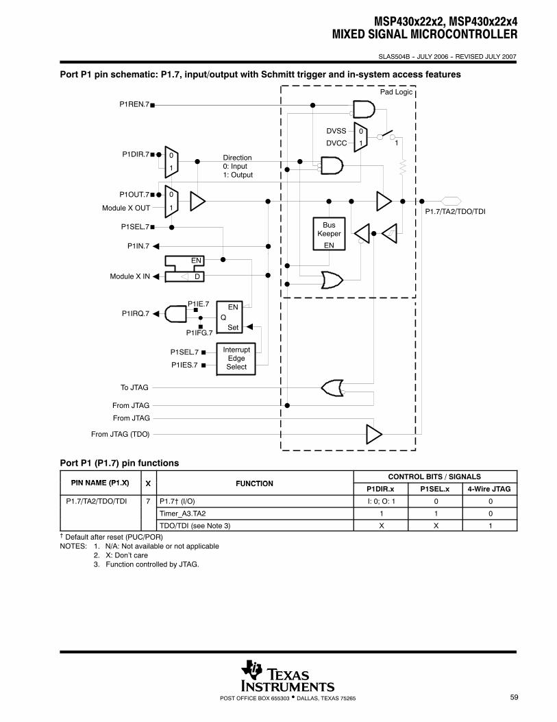
MSP430x22x2, MSP430x22x4MIXED SIGNAL MICROCONTROLLER
SLAS504B -- JULY 2006 -- REVISED JULY 2007
59POST OFFICE BOX 655303 • DALLAS, TEXAS 75265
Port P1 pin schematic: P1.7, input/output with Schmitt trigger and in-system access features
From JTAG
From JTAG (TDO)
BusKeeper
EN
Direction0: Input1: Output
P1SEL.7
1
0P1DIR.7
P1IN.7
P1IRQ.7
D
EN
Module X IN
1
0
Module X OUT
P1OUT.7
InterruptEdgeSelect
QEN
Set
P1SEL.7
P1IES.7
P1IFG.7
P1IE.7
P1.7/TA2/TDO/TDI
1
0DVSS
DVCC
P1REN.7
To JTAG
From JTAG
1
Pad Logic
Port P1 (P1.7) pin functions
PIN NAME (P1 X) X FUNCTIONCONTROL BITS / SIGNALS
PIN NAME (P1.X) X FUNCTIONP1DIR.x P1SEL.x 4-Wire JTAG
P1.7/TA2/TDO/TDI 7 P1.7† (I/O) I: 0; O: 1 0 0/ / /
Timer_A3.TA2 1 1 0
TDO/TDI (see Note 3) X X 1† Default after reset (PUC/POR)NOTES: 1. N/A: Not available or not applicable
2. X: Don’t care3. Function controlled by JTAG.
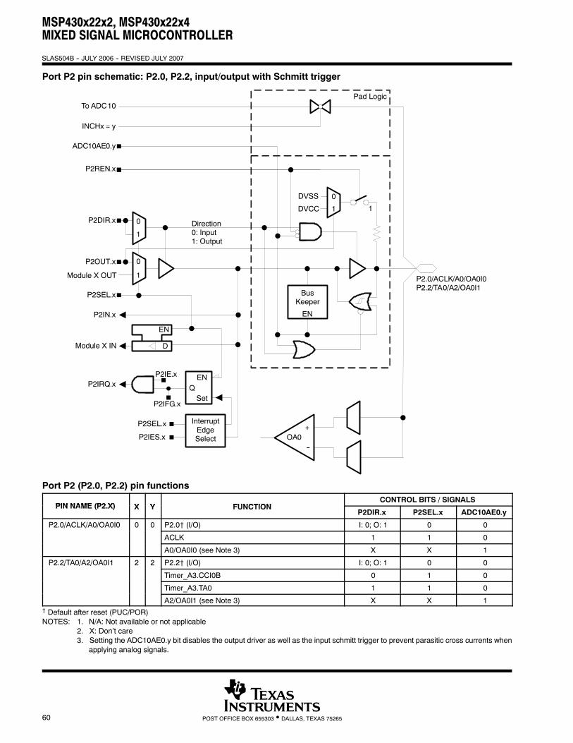
MSP430x22x2, MSP430x22x4MIXED SIGNAL MICROCONTROLLER
SLAS504B -- JULY 2006 -- REVISED JULY 2007
60 POST OFFICE BOX 655303 • DALLAS, TEXAS 75265
Port P2 pin schematic: P2.0, P2.2, input/output with Schmitt trigger
BusKeeper
EN
Direction0: Input1: Output
P2SEL.x
1
0P2DIR.x
P2IN.x
P2IRQ.x
D
EN
Module X IN
1
0
Module X OUT
P2OUT.x
InterruptEdgeSelect
QEN
Set
P2SEL.x
P2IES.x
P2IFG.x
P2IE.x
P2.0/ACLK/A0/OA0I0P2.2/TA0/A2/OA0I1
1
0DVSS
DVCC
P2REN.x
ADC10AE0.y
Pad Logic
INCHx = y
To ADC10
1
OA0+
--
Port P2 (P2.0, P2.2) pin functions
PIN NAME (P2 X) X Y FUNCTIONCONTROL BITS / SIGNALS
PIN NAME (P2.X) X Y FUNCTIONP2DIR.x P2SEL.x ADC10AE0.y
P2.0/ACLK/A0/OA0I0 0 0 P2.0† (I/O) I: 0; O: 1 0 0/ / /
ACLK 1 1 0
A0/OA0I0 (see Note 3) X X 1
P2.2/TA0/A2/OA0I1 2 2 P2.2† (I/O) I: 0; O: 1 0 0/ / /
Timer_A3.CCI0B 0 1 0
Timer_A3.TA0 1 1 0
A2/OA0I1 (see Note 3) X X 1† Default after reset (PUC/POR)NOTES: 1. N/A: Not available or not applicable
2. X: Don’t care3. Setting the ADC10AE0.y bit disables the output driver as well as the input schmitt trigger to prevent parasitic cross currents when
applying analog signals.
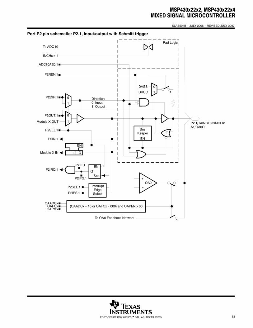
MSP430x22x2, MSP430x22x4MIXED SIGNAL MICROCONTROLLER
SLAS504B -- JULY 2006 -- REVISED JULY 2007
61POST OFFICE BOX 655303 • DALLAS, TEXAS 75265
Port P2 pin schematic: P2.1, input/output with Schmitt trigger
1
OAFCxOAPMx
OAADCx
To OA0 Feedback Network1
(OAADCx = 10 or OAFCx = 000) and OAPMx> 00
BusKeeper
EN
Direction0: Input1: Output
P2SEL.1
1
0P2DIR.1
P2IN.1
P2IRQ.1
D
EN
Module X IN
1
0
Module X OUT
P2OUT.1
InterruptEdgeSelect
QEN
Set
P2SEL.1
P2IES.1
P2IFG.1
P2IE.1
P2.1/TAINCLK/SMCLK/A1/OA0O
1
0DVSS
DVCC
P2REN.1
ADC10AE0.1
Pad Logic
INCHx = 1
To ADC10
1
OA0+
--
1
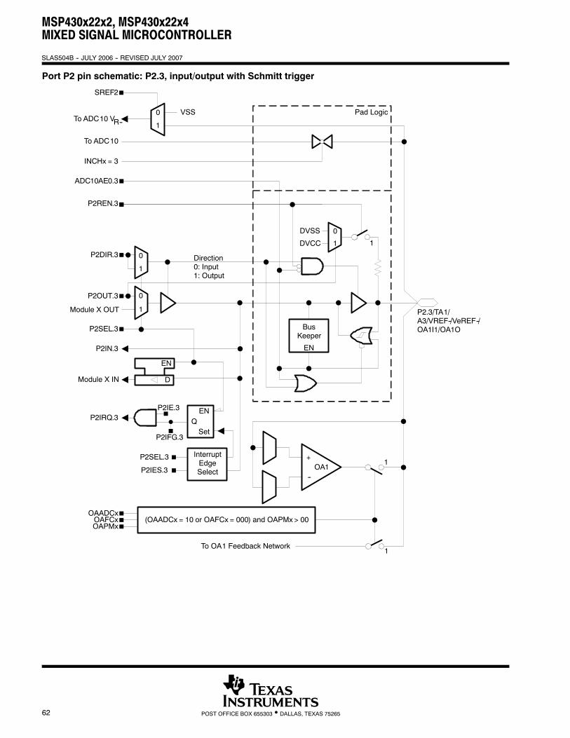
MSP430x22x2, MSP430x22x4MIXED SIGNAL MICROCONTROLLER
SLAS504B -- JULY 2006 -- REVISED JULY 2007
62 POST OFFICE BOX 655303 • DALLAS, TEXAS 75265
Port P2 pin schematic: P2.3, input/output with Schmitt trigger
BusKeeper
EN
Direction0: Input1: Output
P2SEL.3
1
0P2DIR.3
P2IN.3
P2IRQ.3
D
EN
Module X IN
1
0
Module X OUT
P2OUT.3
InterruptEdgeSelect
QEN
Set
P2SEL.3
P2IES.3
P2IFG.3
P2IE.3
1
0DVSS
DVCC
P2REN.3
ADC10AE0.3
Pad Logic
INCHx = 3
To ADC10
1
OA1+
--
1
OAFCxOAPMx
OAADCx
To OA1 Feedback Network
To ADC10 VR-- 1
0
SREF2
VSS
P2.3/TA1/A3/VREF--/VeREF--/OA1I1/OA1O
1
(OAADCx = 10 or OAFCx = 000) and OAPMx> 00
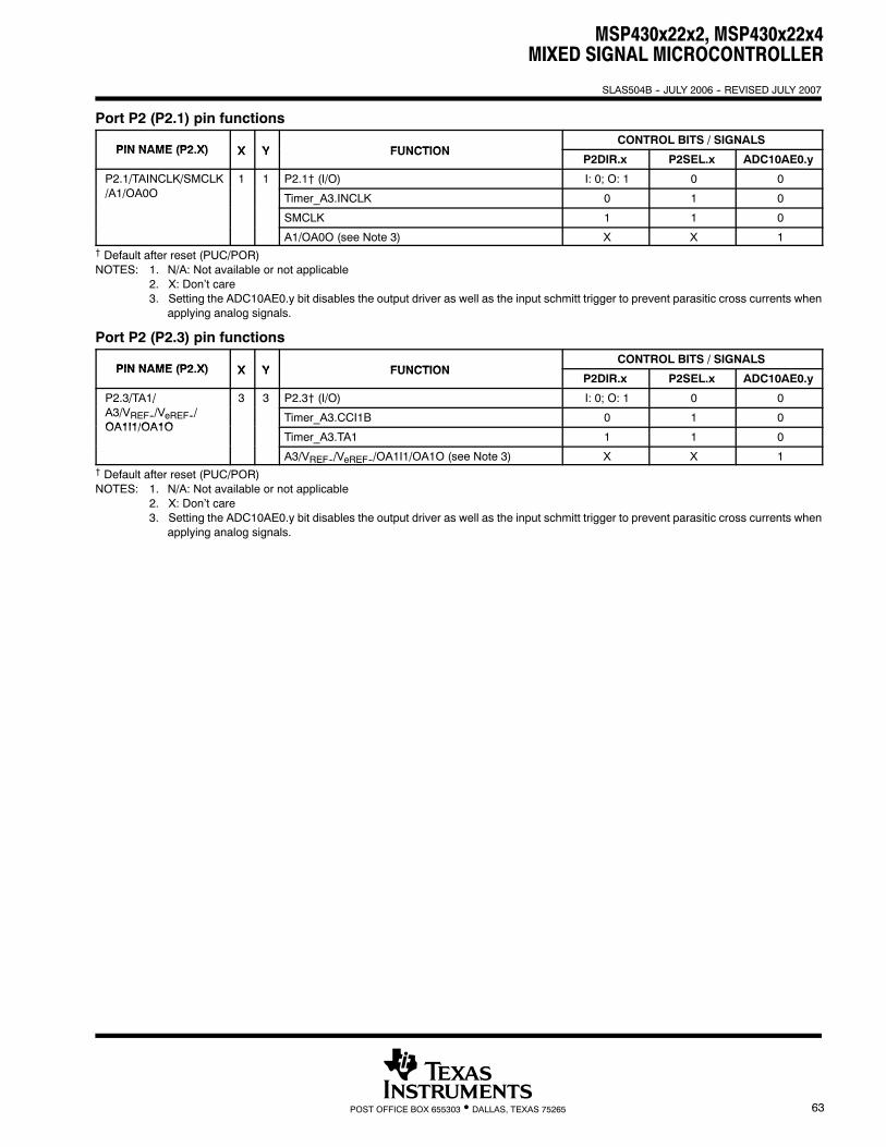
MSP430x22x2, MSP430x22x4MIXED SIGNAL MICROCONTROLLER
SLAS504B -- JULY 2006 -- REVISED JULY 2007
63POST OFFICE BOX 655303 • DALLAS, TEXAS 75265
Port P2 (P2.1) pin functions
PIN NAME (P2 X) X Y FUNCTIONCONTROL BITS / SIGNALS
PIN NAME (P2.X) X Y FUNCTIONP2DIR.x P2SEL.x ADC10AE0.y
P2.1/TAINCLK/SMCLK 1 1 P2.1† (I/O) I: 0; O: 1 0 0/ //A1/OA0O Timer_A3.INCLK 0 1 0
SMCLK 1 1 0
A1/OA0O (see Note 3) X X 1† Default after reset (PUC/POR)NOTES: 1. N/A: Not available or not applicable
2. X: Don’t care3. Setting the ADC10AE0.y bit disables the output driver as well as the input schmitt trigger to prevent parasitic cross currents when
applying analog signals.
Port P2 (P2.3) pin functions
PIN NAME (P2 X) X Y FUNCTIONCONTROL BITS / SIGNALS
PIN NAME (P2.X) X Y FUNCTIONP2DIR.x P2SEL.x ADC10AE0.y
P2.3/TA1/ 3 3 P2.3† (I/O) I: 0; O: 1 0 0/ /A3/VREF--/VeREF--/OA1I1/OA1O
Timer_A3.CCI1B 0 1 0OA1I1/OA1O
Timer_A3.TA1 1 1 0
A3/VREF--/VeREF--/OA1I1/OA1O (see Note 3) X X 1† Default after reset (PUC/POR)NOTES: 1. N/A: Not available or not applicable
2. X: Don’t care3. Setting the ADC10AE0.y bit disables the output driver as well as the input schmitt trigger to prevent parasitic cross currents when
applying analog signals.
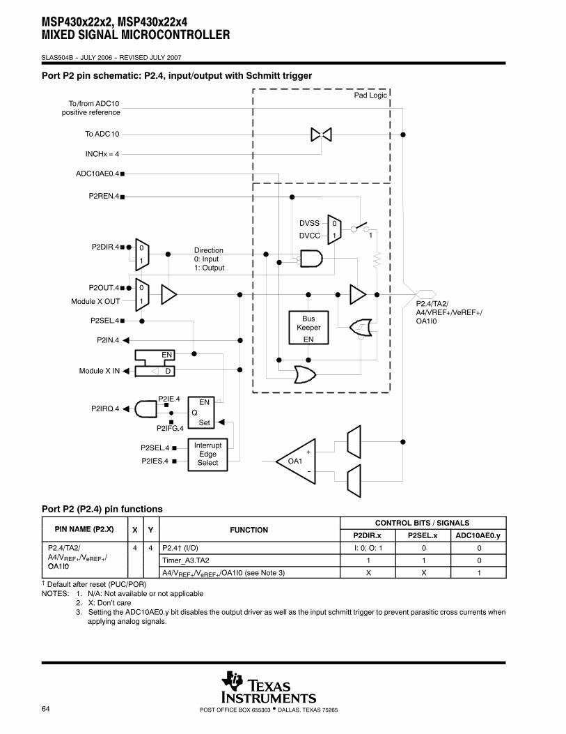
MSP430x22x2, MSP430x22x4MIXED SIGNAL MICROCONTROLLER
SLAS504B -- JULY 2006 -- REVISED JULY 2007
64 POST OFFICE BOX 655303 • DALLAS, TEXAS 75265
Port P2 pin schematic: P2.4, input/output with Schmitt trigger
BusKeeper
EN
Direction0: Input1: Output
P2SEL.4
1
0P2DIR.4
P2IN.4
P2IRQ.4
D
EN
Module X IN
1
0
Module X OUT
P2OUT.4
InterruptEdgeSelect
QEN
Set
P2SEL.4
P2IES.4
P2IFG.4
P2IE.4
P2.4/TA2/A4/VREF+/VeREF+/OA1I0
1
0DVSS
DVCC
P2REN.4
ADC10AE0.4
Pad Logic
INCHx = 4
To ADC10
1
To/from ADC10positive reference
OA1+
--
Port P2 (P2.4) pin functions
PIN NAME (P2 X) X Y FUNCTIONCONTROL BITS / SIGNALS
PIN NAME (P2.X) X Y FUNCTIONP2DIR.x P2SEL.x ADC10AE0.y
P2.4/TA2/ 4 4 P2.4† (I/O) I: 0; O: 1 0 0/ /A4/VREF+/VeREF+/OA1I0
Timer_A3.TA2 1 1 0OA1I0
A4/VREF+/VeREF+/OA1I0 (see Note 3) X X 1† Default after reset (PUC/POR)NOTES: 1. N/A: Not available or not applicable
2. X: Don’t care3. Setting the ADC10AE0.y bit disables the output driver as well as the input schmitt trigger to prevent parasitic cross currents when
applying analog signals.
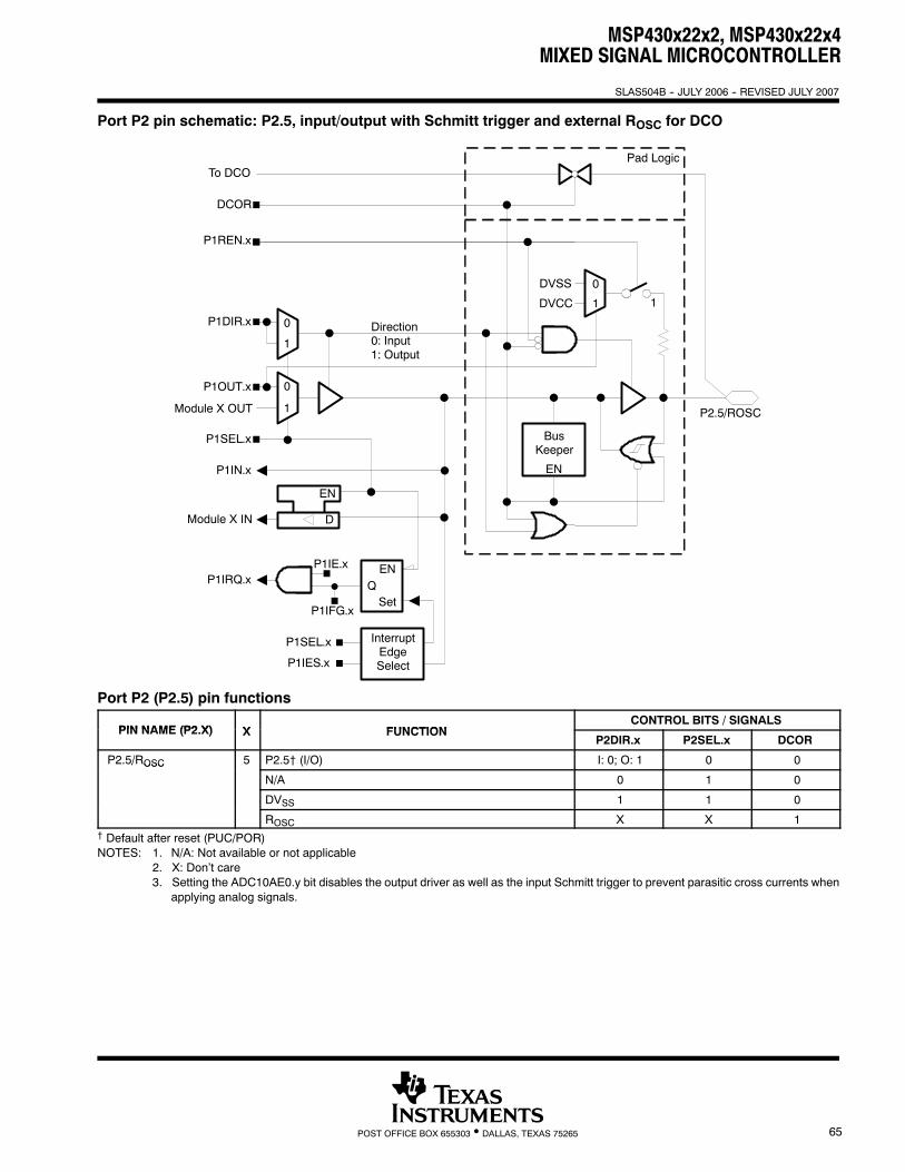
MSP430x22x2, MSP430x22x4MIXED SIGNAL MICROCONTROLLER
SLAS504B -- JULY 2006 -- REVISED JULY 2007
65POST OFFICE BOX 655303 • DALLAS, TEXAS 75265
Port P2 pin schematic: P2.5, input/output with Schmitt trigger and external ROSC for DCO
BusKeeper
EN
Direction0: Input1: Output
P1SEL.x
1
0P1DIR.x
P1IN.x
P1IRQ.x
D
EN
Module X IN
1
0
Module X OUT
P1OUT.x
InterruptEdgeSelect
QEN
Set
P1SEL.x
P1IES.x
P1IFG.x
P1IE.x
P2.5/ROSC
1
0DVSS
DVCC
P1REN.x
DCOR
Pad LogicTo DCO
1
Port P2 (P2.5) pin functions
PIN NAME (P2 X) X FUNCTIONCONTROL BITS / SIGNALS
PIN NAME (P2.X) X FUNCTIONP2DIR.x P2SEL.x DCOR
P2.5/ROSC 5 P2.5† (I/O) I: 0; O: 1 0 0/ OSC
N/A 0 1 0
DVSS 1 1 0
ROSC X X 1† Default after reset (PUC/POR)NOTES: 1. N/A: Not available or not applicable
2. X: Don’t care3. Setting the ADC10AE0.y bit disables the output driver as well as the input Schmitt trigger to prevent parasitic cross currents when
applying analog signals.
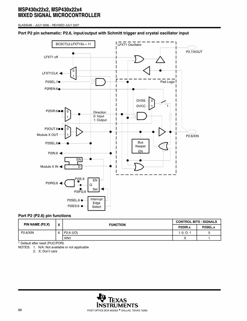
MSP430x22x2, MSP430x22x4MIXED SIGNAL MICROCONTROLLER
SLAS504B -- JULY 2006 -- REVISED JULY 2007
66 POST OFFICE BOX 655303 • DALLAS, TEXAS 75265
Port P2 pin schematic: P2.6, input/output with Schmitt trigger and crystal oscillator input
LFXT1 off
P2SEL.7
BusKeeper
EN
Direction0: Input1: Output
P2SEL.6
1
0P2DIR.6
P2IN.6
P2IRQ.6
D
EN
Module X IN
1
0
Module X OUT
P2OUT.6
InterruptEdgeSelect
QEN
Set
P2SEL.6
P2IES.6
P2IFG.6
P2IE.6
P2.6/XIN
1
0DVSS
DVCC
P2REN.6
Pad Logic
LFXT1 OscillatorBCSCTL3.LFXT1Sx = 11
P2.7/XOUT
0
1
1
LFXT1CLK
Port P2 (P2.6) pin functions
PIN NAME (P2 X) X FUNCTIONCONTROL BITS / SIGNALS
PIN NAME (P2.X) X FUNCTIONP2DIR.x P2SEL.x
P2.6/XIN 6 P2.6 (I/O) I: 0; O: 1 0/
XIN† X 1† Default after reset (PUC/POR)NOTES: 1. N/A: Not available or not applicable
2. X: Don’t care
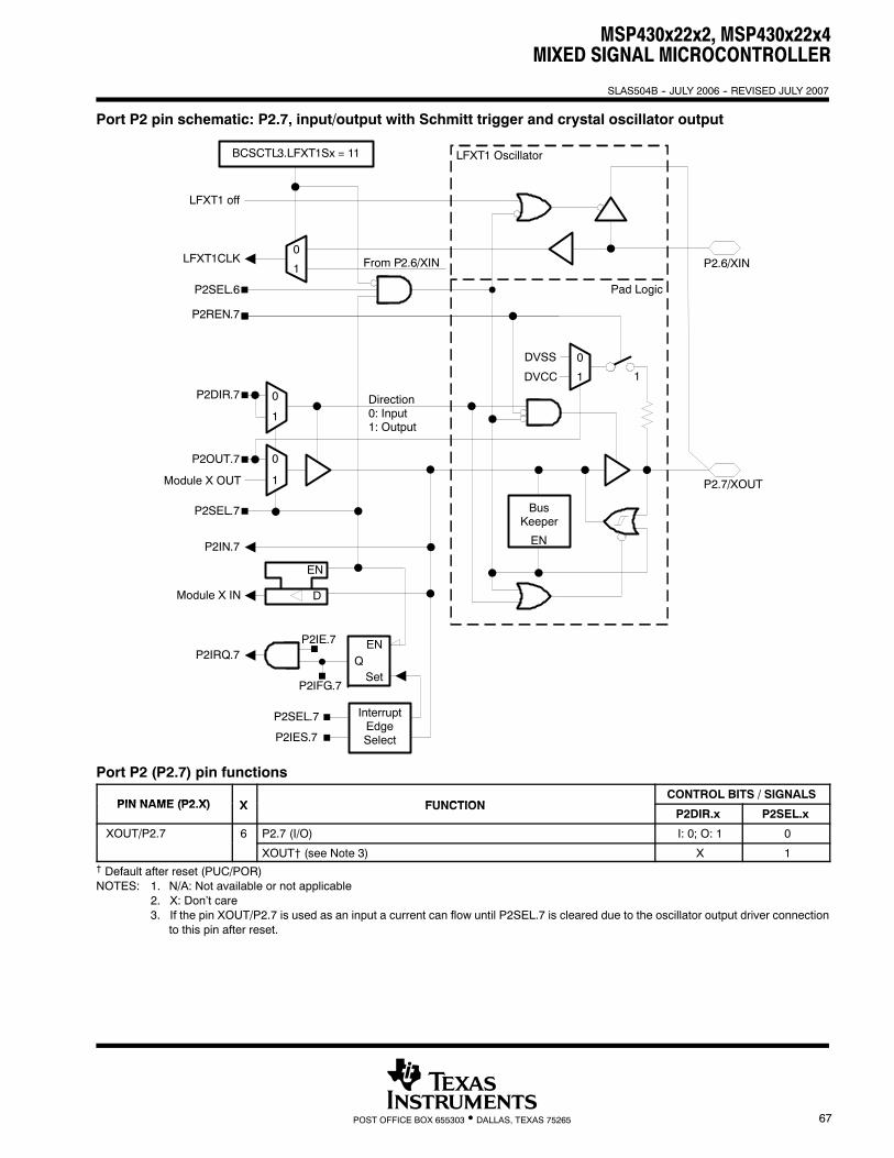
MSP430x22x2, MSP430x22x4MIXED SIGNAL MICROCONTROLLER
SLAS504B -- JULY 2006 -- REVISED JULY 2007
67POST OFFICE BOX 655303 • DALLAS, TEXAS 75265
Port P2 pin schematic: P2.7, input/output with Schmitt trigger and crystal oscillator output
LFXT1 off
P2SEL.6
BusKeeper
EN
Direction0: Input1: Output
P2SEL.7
1
0P2DIR.7
P2IN.7
P2IRQ.7
D
EN
Module X IN
1
0
Module X OUT
P2OUT.7
InterruptEdgeSelect
QEN
Set
P2SEL.7
P2IES.7
P2IFG.7
P2IE.7
P2.7/XOUT
1
0DVSS
DVCC
P2REN.7
Pad Logic
LFXT1 OscillatorBCSCTL3.LFXT1Sx = 11
0
1
1
LFXT1CLK From P2.6/XIN P2.6/XIN
Port P2 (P2.7) pin functions
PIN NAME (P2 X) X FUNCTIONCONTROL BITS / SIGNALS
PIN NAME (P2.X) X FUNCTIONP2DIR.x P2SEL.x
XOUT/P2.7 6 P2.7 (I/O) I: 0; O: 1 0/
XOUT† (see Note 3) X 1† Default after reset (PUC/POR)NOTES: 1. N/A: Not available or not applicable
2. X: Don’t care3. If the pin XOUT/P2.7 is used as an input a current can flow until P2SEL.7 is cleared due to the oscillator output driver connection
to this pin after reset.
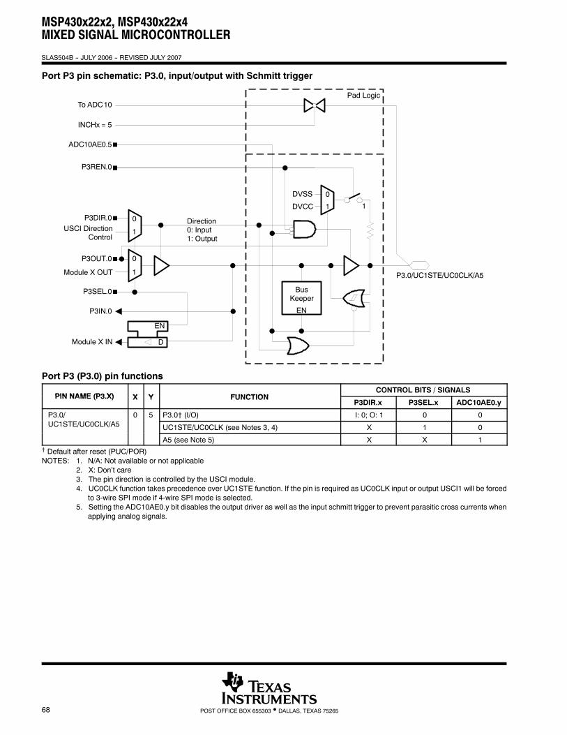
MSP430x22x2, MSP430x22x4MIXED SIGNAL MICROCONTROLLER
SLAS504B -- JULY 2006 -- REVISED JULY 2007
68 POST OFFICE BOX 655303 • DALLAS, TEXAS 75265
Port P3 pin schematic: P3.0, input/output with Schmitt trigger
BusKeeper
EN
Direction0: Input1: Output
P3SEL.0
1
0P3DIR.0
P3IN.0
D
EN
Module X IN
1
0
Module X OUT
P3OUT.0
P3.0/UC1STE/UC0CLK/A5
1
0DVSS
DVCC
P3REN.0
ADC10AE0.5
Pad Logic
INCHx = 5
To ADC10
1
USCI DirectionControl
Port P3 (P3.0) pin functions
PIN NAME (P3 X) X Y FUNCTIONCONTROL BITS / SIGNALS
PIN NAME (P3.X) X Y FUNCTIONP3DIR.x P3SEL.x ADC10AE0.y
P3.0/ 0 5 P3.0† (I/O) I: 0; O: 1 0 0/UC1STE/UC0CLK/A5 UC1STE/UC0CLK (see Notes 3, 4) X 1 0
A5 (see Note 5) X X 1† Default after reset (PUC/POR)NOTES: 1. N/A: Not available or not applicable
2. X: Don’t care3. The pin direction is controlled by the USCI module.4. UC0CLK function takes precedence over UC1STE function. If the pin is required as UC0CLK input or output USCI1 will be forced
to 3-wire SPI mode if 4-wire SPI mode is selected.5. Setting the ADC10AE0.y bit disables the output driver as well as the input schmitt trigger to prevent parasitic cross currents when
applying analog signals.
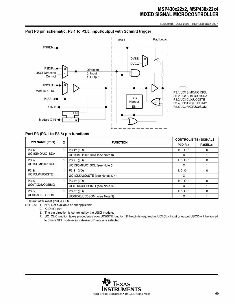
MSP430x22x2, MSP430x22x4MIXED SIGNAL MICROCONTROLLER
SLAS504B -- JULY 2006 -- REVISED JULY 2007
69POST OFFICE BOX 655303 • DALLAS, TEXAS 75265
Port P3 pin schematic: P3.1 to P3.5, input/output with Schmitt trigger
BusKeeper
EN
Direction0: Input1: Output
P3SEL.x
1
0P3DIR.x
P3IN.x
D
EN
Module X IN
1
0
Module X OUT
P3OUT.x
P3.1/UC1SIMO/UC1SCLP3.2/UC1SOMI/UC1SDAP3.3/UC1CLK/UC0STEP3.4/UC0TXD/UC0SIMOP3.5/UC0RXD/UC0SOMI
1
0DVSS
DVCC
P3REN.x
Pad Logic
1
USCI DirectionControl
DVSS
Port P3 (P3.1 to P3.5) pin functions
PIN NAME (P3 X) X FUNCTIONCONTROL BITS / SIGNALS
PIN NAME (P3.X) X FUNCTIONP3DIR.x P3SEL.x
P3.1/ 1 P3.1† (I/O) I: 0; O: 1 0/UC1SIMO/UC1SDA UC1SIMO/UC1SDA (see Note 3) X 1
P3.2/ 1 P3.2† (I/O) I: 0; O: 1 0/UC1SOMI/UC1SCL UC1SOMI/UC1SCL (see Note 3) X 1
P3.3/ 1 P3.3† (I/O) I: 0; O: 1 0/UC1CLK/UC0STE UC1CLK/UC0STE (see Notes 3, 4) X 1
P3.4/ 1 P3.4† (I/O) I: 0; O: 1 0/UC0TXD/UC0SIMO UC0TXD/UC0SIMO (see Note 3) X 1
P3.5/ 1 P3.5† (I/O) I: 0; O: 1 0/UC0RXD/UC0SOMI UC0RXD/UC0SOMI (see Note 3) X 1
† Default after reset (PUC/POR)NOTES: 1. N/A: Not available or not applicable
2. X: Don’t care3. The pin direction is controlled by the USCI module.4. UC1CLK function takes precedence over UC0STE function. If the pin is required as UC1CLK input or output USCI0 will be forced
to 3-wire SPI mode even if 4-wire SPI mode is selected.
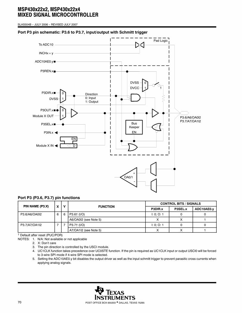
MSP430x22x2, MSP430x22x4MIXED SIGNAL MICROCONTROLLER
SLAS504B -- JULY 2006 -- REVISED JULY 2007
70 POST OFFICE BOX 655303 • DALLAS, TEXAS 75265
Port P3 pin schematic: P3.6 to P3.7, input/output with Schmitt trigger
BusKeeper
EN
Direction0: Input1: Output
P3SEL.x
1
0P3DIR.x
P3IN.x
D
EN
Module X IN
1
0
Module X OUT
P3OUT.x
P3.6/A6/OA0I2P3.7/A7/OA1I2
1
0DVSS
DVCC
P3REN.x
ADC10AE0.y
Pad Logic
INCHx = y
To ADC10
1
OA0/1+
--
DVSS
Port P3 (P3.6, P3.7) pin functions
PIN NAME (P3 X) X Y FUNCTIONCONTROL BITS / SIGNALS
PIN NAME (P3.X) X Y FUNCTIONP3DIR.x P3SEL.x ADC10AE0.y
P3.6/A6/OA0I2 6 6 P3.6† (I/O) I: 0; O: 1 0 0/ /
A6/OA0I2 (see Note 5) X X 1
P3.7/A7/OA1I2 7 7 P3.7† (I/O) I: 0; O: 1 0 0/ /
A7/OA1I2 (see Note 5) X X 1† Default after reset (PUC/POR)NOTES: 1. N/A: Not available or not applicable
2. X: Don’t care3. The pin direction is controlled by the USCI module.4. UC1CLK function takes precedence over UC0STE function. If the pin is required as UC1CLK input or output USCI0 will be forced
to 3-wire SPI mode if 4-wire SPI mode is selected.5. Setting the ADC10AE0.y bit disables the output driver as well as the input schmitt trigger to prevent parasitic cross currents when
applying analog signals.
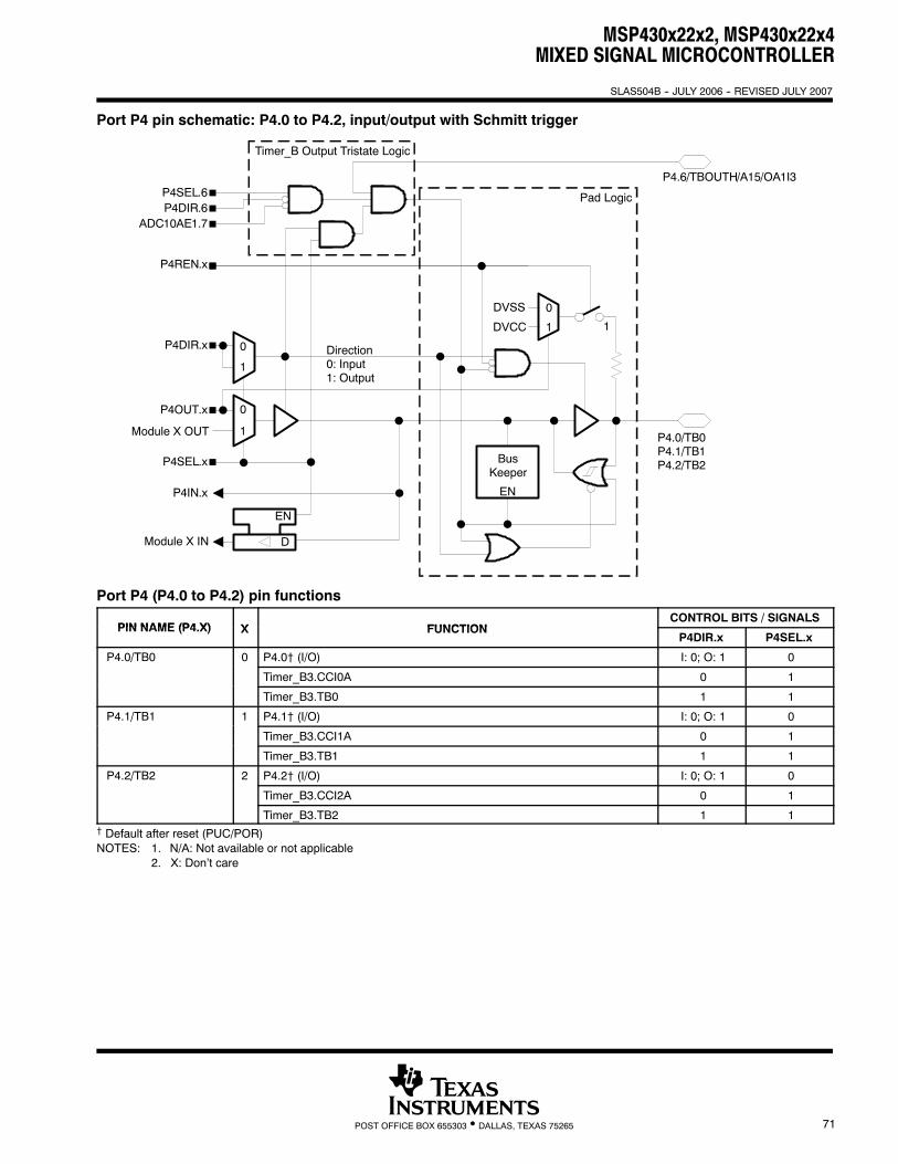
MSP430x22x2, MSP430x22x4MIXED SIGNAL MICROCONTROLLER
SLAS504B -- JULY 2006 -- REVISED JULY 2007
71POST OFFICE BOX 655303 • DALLAS, TEXAS 75265
Port P4 pin schematic: P4.0 to P4.2, input/output with Schmitt trigger
BusKeeper
EN
Direction0: Input1: Output
P4SEL.x
1
0P4DIR.x
P4IN.x
D
EN
Module X IN
1
0
Module X OUT
P4OUT.x
P4.0/TB0P4.1/TB1P4.2/TB2
1
0DVSS
DVCC
P4REN.x
Pad Logic
1
P4DIR.6P4SEL.6
ADC10AE1.7
P4.6/TBOUTH/A15/OA1I3
Timer_B Output Tristate Logic
Port P4 (P4.0 to P4.2) pin functions
PIN NAME (P4 X) X FUNCTIONCONTROL BITS / SIGNALS
PIN NAME (P4.X) X FUNCTIONP4DIR.x P4SEL.x
P4.0/TB0 0 P4.0† (I/O) I: 0; O: 1 0/
Timer_B3.CCI0A 0 1
Timer_B3.TB0 1 1
P4.1/TB1 1 P4.1† (I/O) I: 0; O: 1 0/
Timer_B3.CCI1A 0 1
Timer_B3.TB1 1 1
P4.2/TB2 2 P4.2† (I/O) I: 0; O: 1 0/
Timer_B3.CCI2A 0 1
Timer_B3.TB2 1 1† Default after reset (PUC/POR)NOTES: 1. N/A: Not available or not applicable
2. X: Don’t care
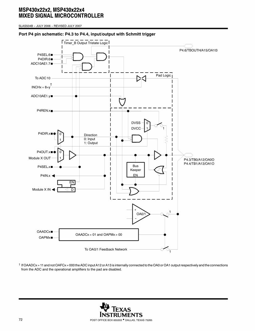
MSP430x22x2, MSP430x22x4MIXED SIGNAL MICROCONTROLLER
SLAS504B -- JULY 2006 -- REVISED JULY 2007
72 POST OFFICE BOX 655303 • DALLAS, TEXAS 75265
Port P4 pin schematic: P4.3 to P4.4, input/output with Schmitt trigger
OAPMx
OAADCx
To OA0/1 Feedback Network1
OAADCx = 01 and OAPMx> 00
BusKeeper
EN
Direction0: Input1: Output
P4SEL.x
1
0P4DIR.x
P4IN.x
D
EN
Module X IN
1
0
Module X OUT
P4OUT.x
P4.3/TB0/A12/OA0OP4.4/TB1/A13/OA1O
1
0DVSS
DVCC
P4REN.x
ADC10AE1.y
Pad Logic
INCHx = 8+y
To ADC10
1
OA0/1+
--
1
P4DIR.6P4SEL.6
ADC10AE1.7
P4.6/TBOUTH/A15/OA1I3
Timer_B Output Tristate Logic
†
† IfOAADCx=11andnotOAFCx=000 theADC inputA12orA13 is internally connected to theOA0orOA1output respectively and theconnectionsfrom the ADC and the operational amplifiers to the pad are disabled.
MSP430x22x2, MSP430x22x4MIXED SIGNAL MICROCONTROLLER
SLAS504B -- JULY 2006 -- REVISED JULY 2007
73POST OFFICE BOX 655303 • DALLAS, TEXAS 75265
Port P4 (P4.3 to P4.4) pin functions
PIN NAME (P4 X) X Y FUNCTIONCONTROL BITS / SIGNALS
PIN NAME (P4.X) X Y FUNCTIONP4DIR.x P4SEL.x ADC10AE1.y
P4.3/TB0/A12/OA0O 3 4 P4.3† (I/O) I: 0; O: 1 0 0/ / /
Timer_B3.CCI0B 0 1 0
Timer_B3.TB0 1 1 0
A12/OA0O (see Note 3) X X 1
P4.4/TB1/A13/OA1O 4 5 P4.4† (I/O) I: 0; O: 1 0 0/ / /
Timer_B3.CCI1B 0 1 0
Timer_B3.TB1 1 1 0
A13/OA1O (see Note 3) X X 1† Default after reset (PUC/POR)NOTES: 1. N/A: Not available or not applicable
2. X: Don’t care3. Setting the ADC10AE1.y bit disables the output driver as well as the input schmitt trigger to prevent parasitic cross currents when
applying analog signals.
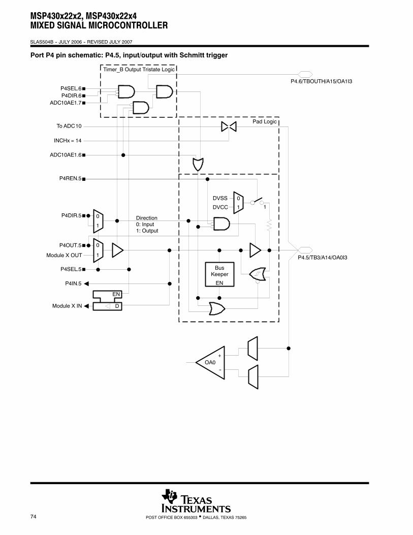
MSP430x22x2, MSP430x22x4MIXED SIGNAL MICROCONTROLLER
SLAS504B -- JULY 2006 -- REVISED JULY 2007
74 POST OFFICE BOX 655303 • DALLAS, TEXAS 75265
Port P4 pin schematic: P4.5, input/output with Schmitt trigger
BusKeeper
EN
Direction0: Input1: Output
P4SEL.5
1
0P4DIR.5
P4IN.5
D
EN
Module X IN
1
0
Module X OUT
P4OUT.5
P4.5/TB3/A14/OA0I3
1
0DVSS
DVCC
P4REN.5
ADC10AE1.6
Pad Logic
INCHx = 14
To ADC10
1
P4DIR.6P4SEL.6
ADC10AE1.7
P4.6/TBOUTH/A15/OA1I3
Timer_B Output Tristate Logic
OA0+
--
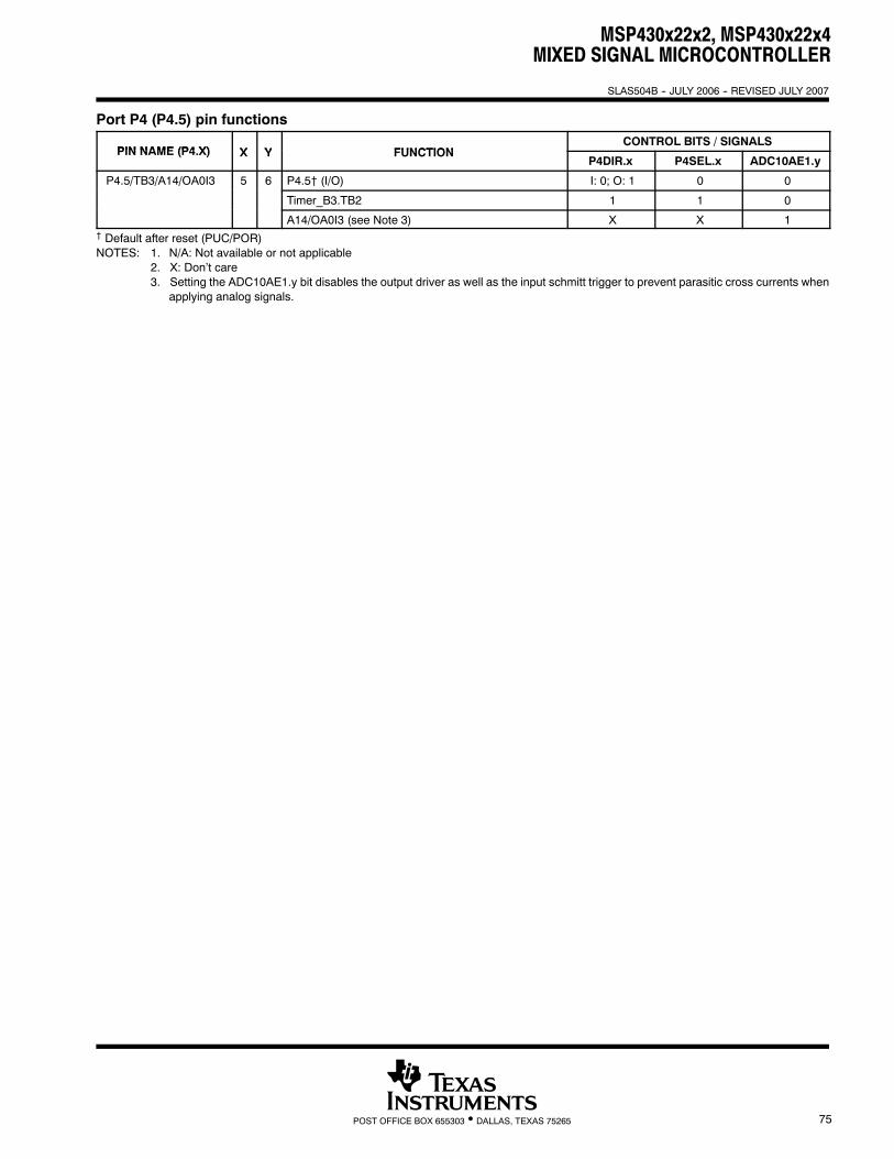
MSP430x22x2, MSP430x22x4MIXED SIGNAL MICROCONTROLLER
SLAS504B -- JULY 2006 -- REVISED JULY 2007
75POST OFFICE BOX 655303 • DALLAS, TEXAS 75265
Port P4 (P4.5) pin functions
PIN NAME (P4 X) X Y FUNCTIONCONTROL BITS / SIGNALS
PIN NAME (P4.X) X Y FUNCTIONP4DIR.x P4SEL.x ADC10AE1.y
P4.5/TB3/A14/OA0I3 5 6 P4.5† (I/O) I: 0; O: 1 0 0/ / /
Timer_B3.TB2 1 1 0
A14/OA0I3 (see Note 3) X X 1† Default after reset (PUC/POR)NOTES: 1. N/A: Not available or not applicable
2. X: Don’t care3. Setting the ADC10AE1.y bit disables the output driver as well as the input schmitt trigger to prevent parasitic cross currents when
applying analog signals.
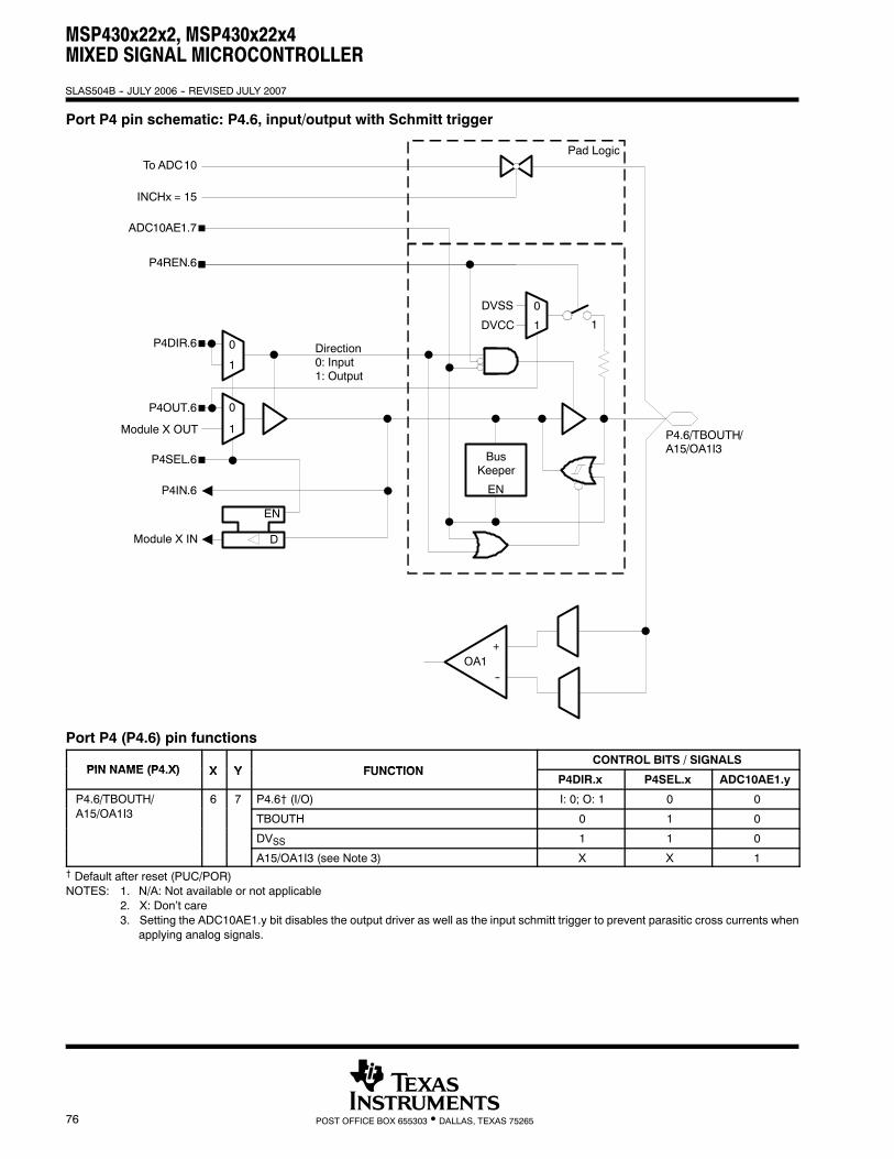
MSP430x22x2, MSP430x22x4MIXED SIGNAL MICROCONTROLLER
SLAS504B -- JULY 2006 -- REVISED JULY 2007
76 POST OFFICE BOX 655303 • DALLAS, TEXAS 75265
Port P4 pin schematic: P4.6, input/output with Schmitt trigger
BusKeeper
EN
Direction0: Input1: Output
P4SEL.6
1
0P4DIR.6
P4IN.6
D
EN
Module X IN
1
0
Module X OUT
P4OUT.6
1
0DVSS
DVCC
P4REN.6
ADC10AE1.7
Pad Logic
INCHx = 15
To ADC10
1
OA1+
--
P4.6/TBOUTH/A15/OA1I3
Port P4 (P4.6) pin functions
PIN NAME (P4 X) X Y FUNCTIONCONTROL BITS / SIGNALS
PIN NAME (P4.X) X Y FUNCTIONP4DIR.x P4SEL.x ADC10AE1.y
P4.6/TBOUTH/ 6 7 P4.6† (I/O) I: 0; O: 1 0 0/ /A15/OA1I3 TBOUTH 0 1 0
DVSS 1 1 0
A15/OA1I3 (see Note 3) X X 1† Default after reset (PUC/POR)NOTES: 1. N/A: Not available or not applicable
2. X: Don’t care3. Setting the ADC10AE1.y bit disables the output driver as well as the input schmitt trigger to prevent parasitic cross currents when
applying analog signals.
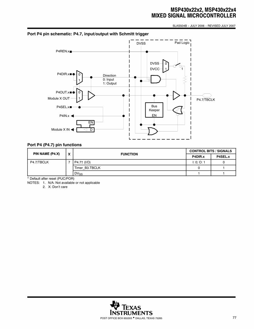
MSP430x22x2, MSP430x22x4MIXED SIGNAL MICROCONTROLLER
SLAS504B -- JULY 2006 -- REVISED JULY 2007
77POST OFFICE BOX 655303 • DALLAS, TEXAS 75265
Port P4 pin schematic: P4.7, input/output with Schmitt trigger
BusKeeper
EN
Direction0: Input1: Output
P4SEL.x
1
0P4DIR.x
P4IN.x
D
EN
Module X IN
1
0
Module X OUT
P4OUT.x
P4.7/TBCLK
1
0DVSS
DVCC
P4REN.x
Pad Logic
1
DVSS
Port P4 (P4.7) pin functions
PIN NAME (P4 X) X FUNCTIONCONTROL BITS / SIGNALS
PIN NAME (P4.X) X FUNCTIONP4DIR.x P4SEL.x
P4.7/TBCLK 7 P4.7† (I/O) I: 0; O: 1 0/
Timer_B3.TBCLK 0 1
DVSS 1 1† Default after reset (PUC/POR)NOTES: 1. N/A: Not available or not applicable
2. X: Don’t care
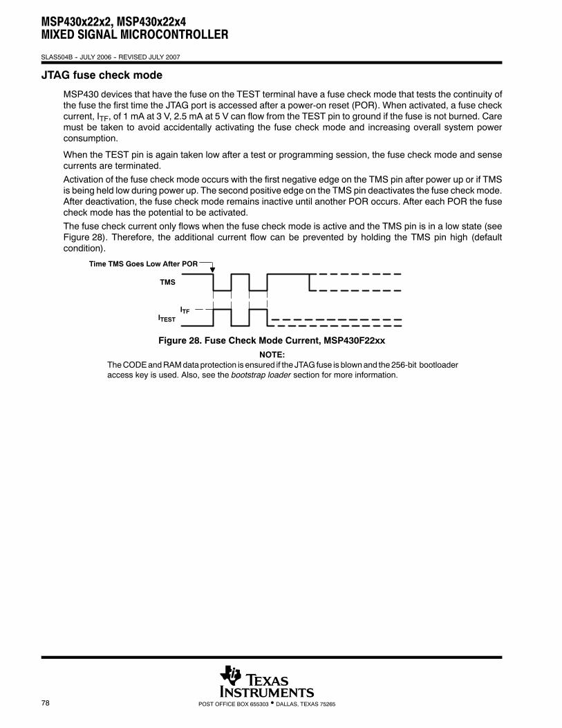
MSP430x22x2, MSP430x22x4MIXED SIGNAL MICROCONTROLLER
SLAS504B -- JULY 2006 -- REVISED JULY 2007
78 POST OFFICE BOX 655303 • DALLAS, TEXAS 75265
JTAG fuse check mode
MSP430 devices that have the fuse on the TEST terminal have a fuse check mode that tests the continuity ofthe fuse the first time the JTAG port is accessed after a power-on reset (POR). When activated, a fuse checkcurrent, ITF, of 1 mA at 3 V, 2.5 mA at 5 V can flow from the TEST pin to ground if the fuse is not burned. Caremust be taken to avoid accidentally activating the fuse check mode and increasing overall system powerconsumption.
When the TEST pin is again taken low after a test or programming session, the fuse check mode and sensecurrents are terminated.Activation of the fuse check mode occurs with the first negative edge on the TMS pin after power up or if TMSis being held low during power up. The second positive edge on the TMS pin deactivates the fuse check mode.After deactivation, the fuse check mode remains inactive until another POR occurs. After each POR the fusecheck mode has the potential to be activated.The fuse check current only flows when the fuse check mode is active and the TMS pin is in a low state (seeFigure 28). Therefore, the additional current flow can be prevented by holding the TMS pin high (defaultcondition).
Time TMS Goes Low After POR
TMS
ITFITEST
Figure 28. Fuse Check Mode Current, MSP430F22xx
NOTE:TheCODEandRAMdataprotection is ensured if the JTAG fuse is blownand the256-bit bootloaderaccess key is used. Also, see the bootstrap loader section for more information.
MSP430x22x2, MSP430x22x4MIXED SIGNAL MICROCONTROLLER
SLAS504B -- JULY 2006 -- REVISED JULY 2007
79POST OFFICE BOX 655303 • DALLAS, TEXAS 75265
Data Sheet Revision History
LiteratureNumber Summary
SLAS504 Preliminary data sheet release.
SLAS504AProduction data sheet release.Updated specification and added characterization graphs.Updated/corrected port pin schematics.
SLAS504BMaximum low-power mode supply current limits decreased.Added note concerning fUCxCLK to USCI SPI parameters.
NOTE: The referring page and figure numbers are referred to the respective document revision.
PACKAGING INFORMATION
Orderable Device Status (1) PackageType
PackageDrawing
Pins PackageQty
Eco Plan (2) Lead/Ball Finish MSL Peak Temp (3)
MSP430F2232IDA ACTIVE TSSOP DA 38 40 Green (RoHS &no Sb/Br)
CU NIPDAU Level-2-260C-1 YEAR
MSP430F2232IDAR ACTIVE TSSOP DA 38 2000 Green (RoHS &no Sb/Br)
CU NIPDAU Level-2-260C-1 YEAR
MSP430F2232IRHAR ACTIVE QFN RHA 40 2500 Green (RoHS &no Sb/Br)
CU NIPDAU Level-3-260C-168 HR
MSP430F2232IRHAT ACTIVE QFN RHA 40 250 Green (RoHS &no Sb/Br)
CU NIPDAU Level-3-260C-168 HR
MSP430F2232TDA ACTIVE TSSOP DA 38 40 Green (RoHS &no Sb/Br)
CU NIPDAU Level-2-260C-1 YEAR
MSP430F2232TDAR ACTIVE TSSOP DA 38 2000 Green (RoHS &no Sb/Br)
CU NIPDAU Level-2-260C-1 YEAR
MSP430F2232TRHAR ACTIVE QFN RHA 40 2500 Green (RoHS &no Sb/Br)
CU NIPDAU Level-3-260C-168 HR
MSP430F2232TRHAT ACTIVE QFN RHA 40 250 Green (RoHS &no Sb/Br)
CU NIPDAU Level-3-260C-168 HR
MSP430F2234IDA ACTIVE TSSOP DA 38 40 Green (RoHS &no Sb/Br)
CU NIPDAU Level-2-260C-1 YEAR
MSP430F2234IDAR ACTIVE TSSOP DA 38 2000 Green (RoHS &no Sb/Br)
CU NIPDAU Level-2-260C-1 YEAR
MSP430F2234IRHAR ACTIVE QFN RHA 40 2500 Green (RoHS &no Sb/Br)
CU NIPDAU Level-3-260C-168 HR
MSP430F2234IRHAT ACTIVE QFN RHA 40 250 Green (RoHS &no Sb/Br)
CU NIPDAU Level-3-260C-168 HR
MSP430F2234TDA ACTIVE TSSOP DA 38 40 Green (RoHS &no Sb/Br)
CU NIPDAU Level-2-260C-1 YEAR
MSP430F2234TDAR ACTIVE TSSOP DA 38 2000 Green (RoHS &no Sb/Br)
CU NIPDAU Level-2-260C-1 YEAR
MSP430F2234TRHAR ACTIVE QFN RHA 40 2500 Green (RoHS &no Sb/Br)
CU NIPDAU Level-3-260C-168 HR
MSP430F2234TRHAT ACTIVE QFN RHA 40 250 Green (RoHS &no Sb/Br)
CU NIPDAU Level-3-260C-168 HR
MSP430F2252IDA ACTIVE TSSOP DA 38 40 Green (RoHS &no Sb/Br)
CU NIPDAU Level-2-260C-1 YEAR
MSP430F2252IDAR ACTIVE TSSOP DA 38 2000 Green (RoHS &no Sb/Br)
CU NIPDAU Level-2-260C-1 YEAR
MSP430F2252IRHAR ACTIVE QFN RHA 40 2500 Green (RoHS &no Sb/Br)
CU NIPDAU Level-3-260C-168 HR
MSP430F2252IRHAT ACTIVE QFN RHA 40 250 Green (RoHS &no Sb/Br)
CU NIPDAU Level-3-260C-168 HR
MSP430F2252TDA ACTIVE TSSOP DA 38 40 Green (RoHS &no Sb/Br)
CU NIPDAU Level-2-260C-1 YEAR
MSP430F2252TDAR ACTIVE TSSOP DA 38 2000 Green (RoHS &no Sb/Br)
CU NIPDAU Level-2-260C-1 YEAR
MSP430F2252TRHAR ACTIVE QFN RHA 40 2500 Green (RoHS &no Sb/Br)
CU NIPDAU Level-3-260C-168 HR
MSP430F2252TRHAT ACTIVE QFN RHA 40 250 Green (RoHS &no Sb/Br)
CU NIPDAU Level-3-260C-168 HR
MSP430F2254IDA ACTIVE TSSOP DA 38 40 Green (RoHS &no Sb/Br)
CU NIPDAU Level-2-260C-1 YEAR
PACKAGE OPTION ADDENDUM
www.ti.com 18-Sep-2008
Addendum-Page 1
Orderable Device Status (1) PackageType
PackageDrawing
Pins PackageQty
Eco Plan (2) Lead/Ball Finish MSL Peak Temp (3)
MSP430F2254IDAR ACTIVE TSSOP DA 38 2000 Green (RoHS &no Sb/Br)
CU NIPDAU Level-2-260C-1 YEAR
MSP430F2254IRHAR ACTIVE QFN RHA 40 2500 Green (RoHS &no Sb/Br)
CU NIPDAU Level-3-260C-168 HR
MSP430F2254IRHAT ACTIVE QFN RHA 40 250 Green (RoHS &no Sb/Br)
CU NIPDAU Level-3-260C-168 HR
MSP430F2254TDA ACTIVE TSSOP DA 38 40 Green (RoHS &no Sb/Br)
CU NIPDAU Level-2-260C-1 YEAR
MSP430F2254TDAR ACTIVE TSSOP DA 38 2000 Green (RoHS &no Sb/Br)
CU NIPDAU Level-2-260C-1 YEAR
MSP430F2254TRHAR ACTIVE QFN RHA 40 2500 Green (RoHS &no Sb/Br)
CU NIPDAU Level-3-260C-168 HR
MSP430F2254TRHAT ACTIVE QFN RHA 40 250 Green (RoHS &no Sb/Br)
CU NIPDAU Level-3-260C-168 HR
MSP430F2272IDA ACTIVE TSSOP DA 38 40 Green (RoHS &no Sb/Br)
CU NIPDAU Level-2-260C-1 YEAR
MSP430F2272IDAR ACTIVE TSSOP DA 38 2000 Green (RoHS &no Sb/Br)
CU NIPDAU Level-2-260C-1 YEAR
MSP430F2272IRHAR ACTIVE QFN RHA 40 2500 Green (RoHS &no Sb/Br)
CU NIPDAU Level-3-260C-168 HR
MSP430F2272IRHAT ACTIVE QFN RHA 40 250 Green (RoHS &no Sb/Br)
CU NIPDAU Level-3-260C-168 HR
MSP430F2272TDA ACTIVE TSSOP DA 38 40 Green (RoHS &no Sb/Br)
CU NIPDAU Level-2-260C-1 YEAR
MSP430F2272TDAR ACTIVE TSSOP DA 38 2000 Green (RoHS &no Sb/Br)
CU NIPDAU Level-2-260C-1 YEAR
MSP430F2272TRHAR ACTIVE QFN RHA 40 2500 Green (RoHS &no Sb/Br)
CU NIPDAU Level-3-260C-168 HR
MSP430F2272TRHAT ACTIVE QFN RHA 40 250 Green (RoHS &no Sb/Br)
CU NIPDAU Level-3-260C-168 HR
MSP430F2274IDA ACTIVE TSSOP DA 38 40 Green (RoHS &no Sb/Br)
CU NIPDAU Level-2-260C-1 YEAR
MSP430F2274IDAR ACTIVE TSSOP DA 38 2000 Green (RoHS &no Sb/Br)
CU NIPDAU Level-2-260C-1 YEAR
MSP430F2274IRHAR ACTIVE QFN RHA 40 2500 Green (RoHS &no Sb/Br)
CU NIPDAU Level-3-260C-168 HR
MSP430F2274IRHAT ACTIVE QFN RHA 40 250 Green (RoHS &no Sb/Br)
CU NIPDAU Level-3-260C-168 HR
MSP430F2274TDA ACTIVE TSSOP DA 38 40 Green (RoHS &no Sb/Br)
CU NIPDAU Level-2-260C-1 YEAR
MSP430F2274TDAR ACTIVE TSSOP DA 38 2000 Green (RoHS &no Sb/Br)
CU NIPDAU Level-2-260C-1 YEAR
MSP430F2274TRHAR ACTIVE QFN RHA 40 2500 Green (RoHS &no Sb/Br)
CU NIPDAU Level-3-260C-168 HR
MSP430F2274TRHAT ACTIVE QFN RHA 40 250 Green (RoHS &no Sb/Br)
CU NIPDAU Level-3-260C-168 HR
(1) The marketing status values are defined as follows:ACTIVE: Product device recommended for new designs.LIFEBUY: TI has announced that the device will be discontinued, and a lifetime-buy period is in effect.NRND: Not recommended for new designs. Device is in production to support existing customers, but TI does not recommend using this part ina new design.PREVIEW: Device has been announced but is not in production. Samples may or may not be available.
PACKAGE OPTION ADDENDUM
www.ti.com 18-Sep-2008
Addendum-Page 2

OBSOLETE: TI has discontinued the production of the device.
(2) Eco Plan - The planned eco-friendly classification: Pb-Free (RoHS), Pb-Free (RoHS Exempt), or Green (RoHS & no Sb/Br) - please checkhttp://www.ti.com/productcontent for the latest availability information and additional product content details.TBD: The Pb-Free/Green conversion plan has not been defined.Pb-Free (RoHS): TI's terms "Lead-Free" or "Pb-Free" mean semiconductor products that are compatible with the current RoHS requirementsfor all 6 substances, including the requirement that lead not exceed 0.1% by weight in homogeneous materials. Where designed to be solderedat high temperatures, TI Pb-Free products are suitable for use in specified lead-free processes.Pb-Free (RoHS Exempt): This component has a RoHS exemption for either 1) lead-based flip-chip solder bumps used between the die andpackage, or 2) lead-based die adhesive used between the die and leadframe. The component is otherwise considered Pb-Free (RoHScompatible) as defined above.Green (RoHS & no Sb/Br): TI defines "Green" to mean Pb-Free (RoHS compatible), and free of Bromine (Br) and Antimony (Sb) based flameretardants (Br or Sb do not exceed 0.1% by weight in homogeneous material)
(3) MSL, Peak Temp. -- The Moisture Sensitivity Level rating according to the JEDEC industry standard classifications, and peak soldertemperature.
Important Information and Disclaimer:The information provided on this page represents TI's knowledge and belief as of the date that it isprovided. TI bases its knowledge and belief on information provided by third parties, and makes no representation or warranty as to theaccuracy of such information. Efforts are underway to better integrate information from third parties. TI has taken and continues to takereasonable steps to provide representative and accurate information but may not have conducted destructive testing or chemical analysis onincoming materials and chemicals. TI and TI suppliers consider certain information to be proprietary, and thus CAS numbers and other limitedinformation may not be available for release.
In no event shall TI's liability arising out of such information exceed the total purchase price of the TI part(s) at issue in this document sold by TIto Customer on an annual basis.
OTHER QUALIFIED VERSIONS OF MSP430F2274 :
• Enhanced Product: MSP430F2274-EP
NOTE: Qualified Version Definitions:
• Enhanced Product - Supports Defense, Aerospace and Medical Applications
PACKAGE OPTION ADDENDUM
www.ti.com 18-Sep-2008
Addendum-Page 3
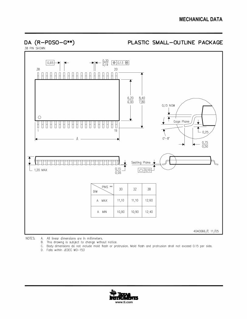
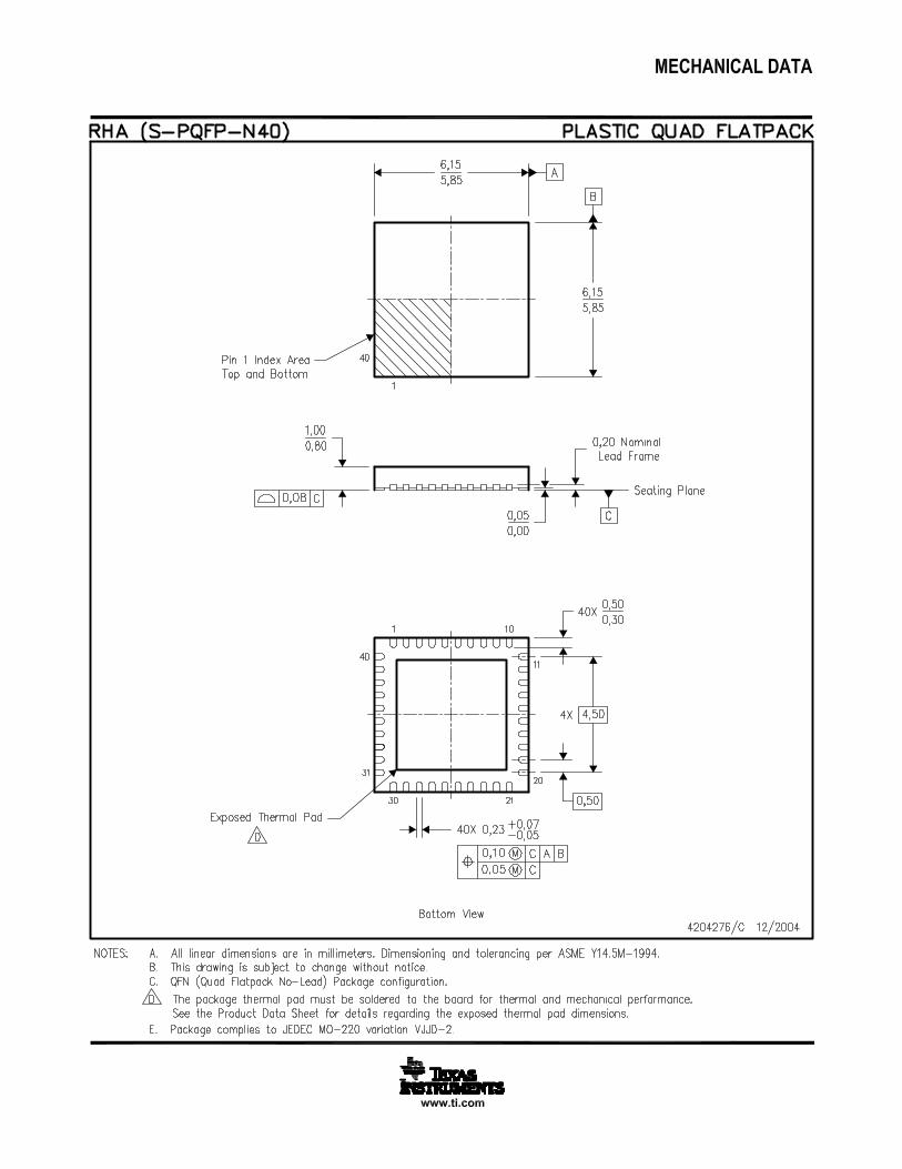
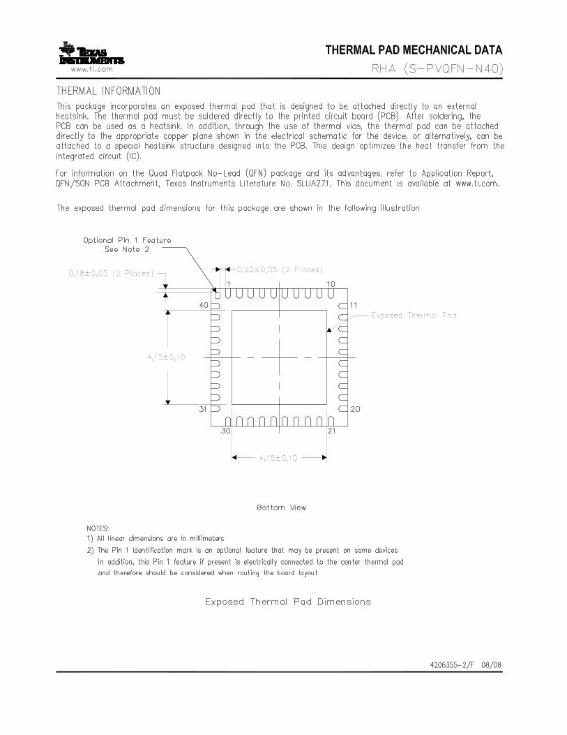
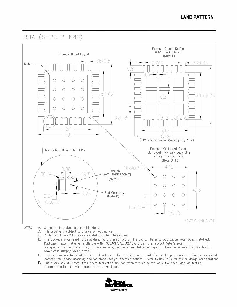
IMPORTANT NOTICETexas Instruments Incorporated and its subsidiaries (TI) reserve the right to make corrections, modifications, enhancements, improvements,and other changes to its products and services at any time and to discontinue any product or service without notice. Customers shouldobtain the latest relevant information before placing orders and should verify that such information is current and complete. All products aresold subject to TI’s terms and conditions of sale supplied at the time of order acknowledgment.TI warrants performance of its hardware products to the specifications applicable at the time of sale in accordance with TI’s standardwarranty. Testing and other quality control techniques are used to the extent TI deems necessary to support this warranty. Except wheremandated by government requirements, testing of all parameters of each product is not necessarily performed.TI assumes no liability for applications assistance or customer product design. Customers are responsible for their products andapplications using TI components. To minimize the risks associated with customer products and applications, customers should provideadequate design and operating safeguards.TI does not warrant or represent that any license, either express or implied, is granted under any TI patent right, copyright, mask work right,or other TI intellectual property right relating to any combination, machine, or process in which TI products or services are used. Informationpublished by TI regarding third-party products or services does not constitute a license from TI to use such products or services or awarranty or endorsement thereof. Use of such information may require a license from a third party under the patents or other intellectualproperty of the third party, or a license from TI under the patents or other intellectual property of TI.Reproduction of TI information in TI data books or data sheets is permissible only if reproduction is without alteration and is accompaniedby all associated warranties, conditions, limitations, and notices. Reproduction of this information with alteration is an unfair and deceptivebusiness practice. TI is not responsible or liable for such altered documentation. Information of third parties may be subject to additionalrestrictions.Resale of TI products or services with statements different from or beyond the parameters stated by TI for that product or service voids allexpress and any implied warranties for the associated TI product or service and is an unfair and deceptive business practice. TI is notresponsible or liable for any such statements.TI products are not authorized for use in safety-critical applications (such as life support) where a failure of the TI product would reasonablybe expected to cause severe personal injury or death, unless officers of the parties have executed an agreement specifically governingsuch use. Buyers represent that they have all necessary expertise in the safety and regulatory ramifications of their applications, andacknowledge and agree that they are solely responsible for all legal, regulatory and safety-related requirements concerning their productsand any use of TI products in such safety-critical applications, notwithstanding any applications-related information or support that may beprovided by TI. Further, Buyers must fully indemnify TI and its representatives against any damages arising out of the use of TI products insuch safety-critical applications.TI products are neither designed nor intended for use in military/aerospace applications or environments unless the TI products arespecifically designated by TI as military-grade or "enhanced plastic." Only products designated by TI as military-grade meet militaryspecifications. Buyers acknowledge and agree that any such use of TI products which TI has not designated as military-grade is solely atthe Buyer's risk, and that they are solely responsible for compliance with all legal and regulatory requirements in connection with such use.TI products are neither designed nor intended for use in automotive applications or environments unless the specific TI products aredesignated by TI as compliant with ISO/TS 16949 requirements. Buyers acknowledge and agree that, if they use any non-designatedproducts in automotive applications, TI will not be responsible for any failure to meet such requirements.Following are URLs where you can obtain information on other Texas Instruments products and application solutions:Products ApplicationsAmplifiers amplifier.ti.com Audio www.ti.com/audioData Converters dataconverter.ti.com Automotive www.ti.com/automotiveDSP dsp.ti.com Broadband www.ti.com/broadbandClocks and Timers www.ti.com/clocks Digital Control www.ti.com/digitalcontrolInterface interface.ti.com Medical www.ti.com/medicalLogic logic.ti.com Military www.ti.com/militaryPower Mgmt power.ti.com Optical Networking www.ti.com/opticalnetworkMicrocontrollers microcontroller.ti.com Security www.ti.com/securityRFID www.ti-rfid.com Telephony www.ti.com/telephonyRF/IF and ZigBee® Solutions www.ti.com/lprf Video & Imaging www.ti.com/video
Wireless www.ti.com/wireless
Mailing Address: Texas Instruments, Post Office Box 655303, Dallas, Texas 75265Copyright © 2008, Texas Instruments Incorporated