Modulo Sequencial ate 256 Canais - Manual Sonigate
14
1/13 November 2003 STP6NK90Z - STP6NK90ZFP STB6NK90Z - STW7NK90Z N-CHANNEL 900V - 1.56Ω - 5.8A TO-220/FP/D 2 PAK/TO-247 Zener-Protected SuperMESH™Power MOSFET ■ TYPICAL R DS (on) = 1.56 Ω ■ EXTREMELY HIGH dv/dt CAPABILITY ■ 100% AVALANCHE TESTED ■ GATE CHARGE MINIMIZED ■ VERY LOW INTRINSIC CAPACITANCES ■ VERY GOOD MANUFACTURING REPEATIBILITY DESCRIPTION The SuperMESH™ series is obtained through an extreme optimization of ST’s well established strip- based PowerMESH™ layout. In addition to pushing on-resistance significantly down, special care is tak- en to ensure a very good dv/dt capability for the most demanding applications. Such series comple- ments ST full range of high voltage MOSFETs in- cluding revolutionary MDmesh™ products. APPLICATIONS ■ HIGH CURRENT, HIGH SPEED SWITCHING ■ IDEAL FOR OFF-LINE POWER SUPPLIES, ADAPTORS AND PFC ■ LIGHTING ORDERING INFORMATION TYPE V DSS R DS(on) I D Pw STP6NK90Z STP6NK90ZFP STB6NK90Z STW7NK90Z 900 V 900 V 900 V 900 V <2 Ω <2 Ω <2 Ω <2 Ω 5.8 A 5.8 A 5.8 A 5.8 A 140 W 30 W 140 W 140 W SALES TYPE MARKING PACKAGE PACKAGING STP6NK90Z P6NK90Z TO-220 TUBE STP6NK90ZFP P6NK90ZFP TO-220FP TUBE STB6NK90ZT4 B6NK90Z D 2 PAK TAPE & REEL STW7NK90Z W7NK90Z TO-247 TUBE TO-220 1 2 3 1 3 1 2 3 TO-247 TO-220FP D 2 PAK INTERNAL SCHEMATIC DIAGRAM
description
DESCRIPTION TheSuperMESH™seriesisobtainedthroughan extremeoptimizationofST’swellestablishedstrip- basedPowerMESH™layout.Inadditiontopushing on-resistancesignificantlydown,specialcareistak- entoensureaverygooddv/dtcapabilityforthe mostdemandingapplications.Suchseriescomple- mentsSTfullrangeofhighvoltageMOSFETsin- cludingrevolutionaryMDmesh™products. INTERNALSCHEMATICDIAGRAM ORDERINGINFORMATION 140W 30W 140W 140W D 2 PAK TO-220FP TO-247 TO-220 900V 900V 900V 900V 5.8A 5.8A 5.8A 5.8A 1 2
Transcript of Modulo Sequencial ate 256 Canais - Manual Sonigate
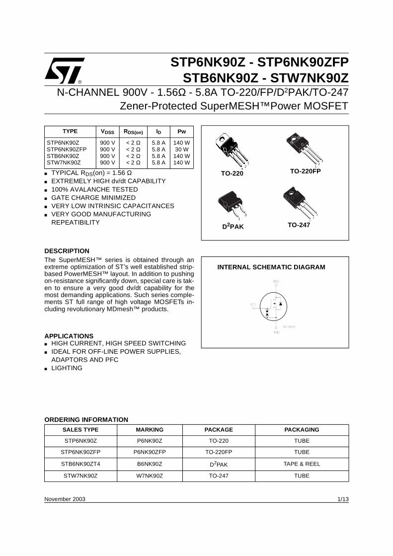
1/13November 2003
STP6NK90Z - STP6NK90ZFPSTB6NK90Z - STW7NK90Z
N-CHANNEL 900V - 1.56Ω - 5.8A TO-220/FP/D2PAK/TO-247Zener-Protected SuperMESH™Power MOSFET
TYPICAL RDS(on) = 1.56 Ω EXTREMELY HIGH dv/dt CAPABILITY 100% AVALANCHE TESTED GATE CHARGE MINIMIZED VERY LOW INTRINSIC CAPACITANCES VERY GOOD MANUFACTURING
REPEATIBILITY
DESCRIPTIONThe SuperMESH™ series is obtained through anextreme optimization of ST’s well established strip-based PowerMESH™ layout. In addition to pushingon-resistance significantly down, special care is tak-en to ensure a very good dv/dt capability for themost demanding applications. Such series comple-ments ST full range of high voltage MOSFETs in-cluding revolutionary MDmesh™ products.
APPLICATIONS HIGH CURRENT, HIGH SPEED SWITCHING IDEAL FOR OFF-LINE POWER SUPPLIES,
ADAPTORS AND PFC LIGHTING
ORDERING INFORMATION
TYPE VDSS RDS(on) ID Pw
STP6NK90ZSTP6NK90ZFPSTB6NK90ZSTW7NK90Z
900 V900 V900 V900 V
< 2 Ω< 2 Ω< 2 Ω< 2 Ω
5.8 A5.8 A5.8 A5.8 A
140 W30 W
140 W140 W
SALES TYPE MARKING PACKAGE PACKAGING
STP6NK90Z P6NK90Z TO-220 TUBE
STP6NK90ZFP P6NK90ZFP TO-220FP TUBE
STB6NK90ZT4 B6NK90Z D2PAK TAPE & REEL
STW7NK90Z W7NK90Z TO-247 TUBE
TO-2201
23
13
12
3
TO-247
TO-220FP
D2PAK
INTERNAL SCHEMATIC DIAGRAM
STP6NK90Z - STP6NK90ZFP - STB6NK90Z - STW7NK90Z
2/13
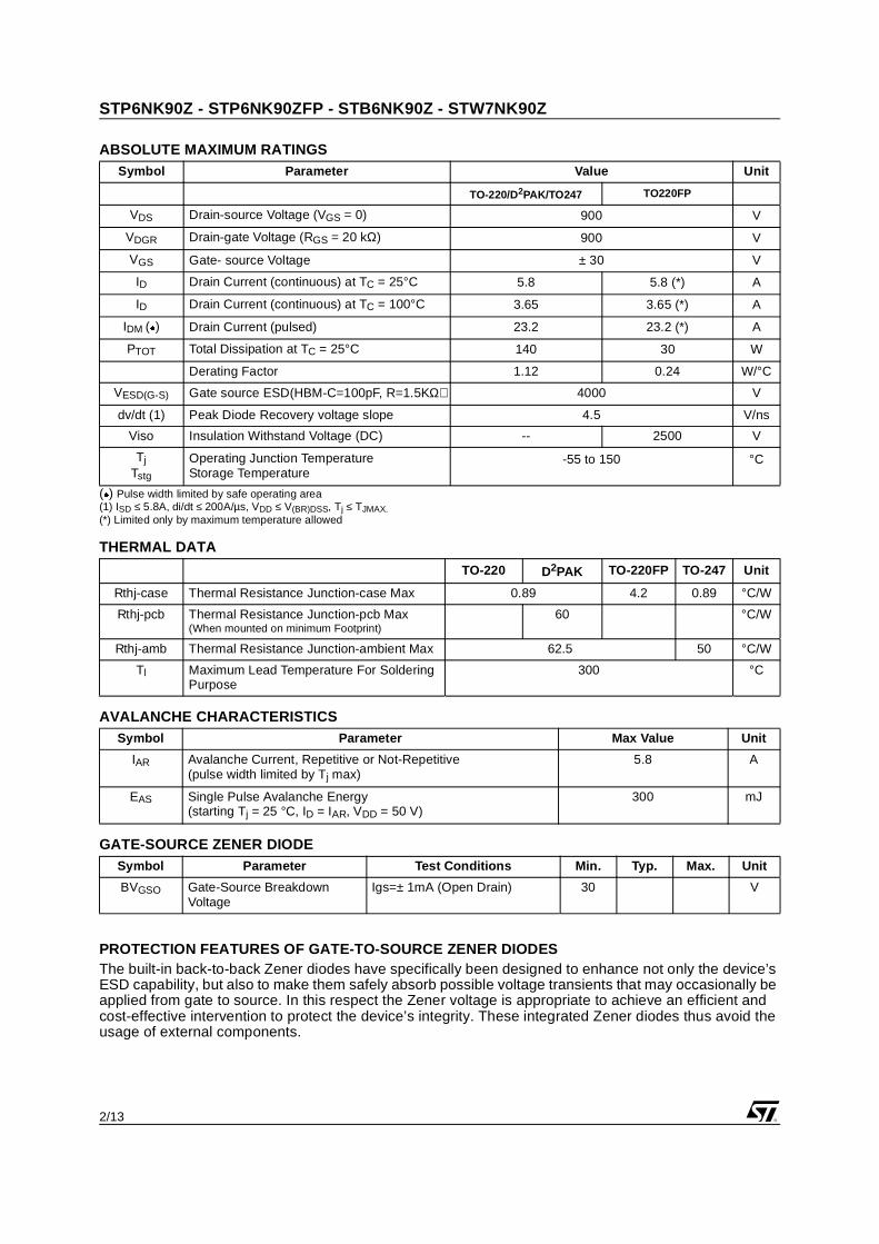
ABSOLUTE MAXIMUM RATINGS
() Pulse width limited by safe operating area(1) ISD ≤ 5.8A, di/dt ≤ 200A/µs, VDD ≤ V(BR)DSS, Tj ≤ TJMAX.(*) Limited only by maximum temperature allowed
THERMAL DATA
AVALANCHE CHARACTERISTICS
GATE-SOURCE ZENER DIODE
PROTECTION FEATURES OF GATE-TO-SOURCE ZENER DIODESThe built-in back-to-back Zener diodes have specifically been designed to enhance not only the device’sESD capability, but also to make them safely absorb possible voltage transients that may occasionally beapplied from gate to source. In this respect the Zener voltage is appropriate to achieve an efficient andcost-effective intervention to protect the device’s integrity. These integrated Zener diodes thus avoid theusage of external components.
Symbol Parameter Value Unit
TO-220/D2PAK/TO247 TO220FP
VDS Drain-source Voltage (VGS = 0) 900 V
VDGR Drain-gate Voltage (RGS = 20 kΩ) 900 V
VGS Gate- source Voltage ± 30 V
ID Drain Current (continuous) at TC = 25°C 5.8 5.8 (*) A
ID Drain Current (continuous) at TC = 100°C 3.65 3.65 (*) A
IDM () Drain Current (pulsed) 23.2 23.2 (*) A
PTOT Total Dissipation at TC = 25°C 140 30 W
Derating Factor 1.12 0.24 W/°C
VESD(G-S) Gate source ESD(HBM-C=100pF, R=1.5KΩ) 4000 V
dv/dt (1) Peak Diode Recovery voltage slope 4.5 V/ns
Viso Insulation Withstand Voltage (DC) -- 2500 V
TjTstg
Operating Junction TemperatureStorage Temperature
-55 to 150 °C
TO-220 D2PAK TO-220FP TO-247 Unit
Rthj-case Thermal Resistance Junction-case Max 0.89 4.2 0.89 °C/W
Rthj-pcb Thermal Resistance Junction-pcb Max(When mounted on minimum Footprint)
60 °C/W
Rthj-amb Thermal Resistance Junction-ambient Max 62.5 50 °C/W
Tl Maximum Lead Temperature For SolderingPurpose
300 °C
Symbol Parameter Max Value Unit
IAR Avalanche Current, Repetitive or Not-Repetitive(pulse width limited by Tj max)
5.8 A
EAS Single Pulse Avalanche Energy(starting Tj = 25 °C, ID = IAR, VDD = 50 V)
300 mJ
Symbol Parameter Test Conditions Min. Typ. Max. Unit
BVGSO Gate-Source BreakdownVoltage
Igs=± 1mA (Open Drain) 30 V
3/13
STP6NK90Z - STP6NK90ZFP - STB6NK90Z - STW7NK90Z
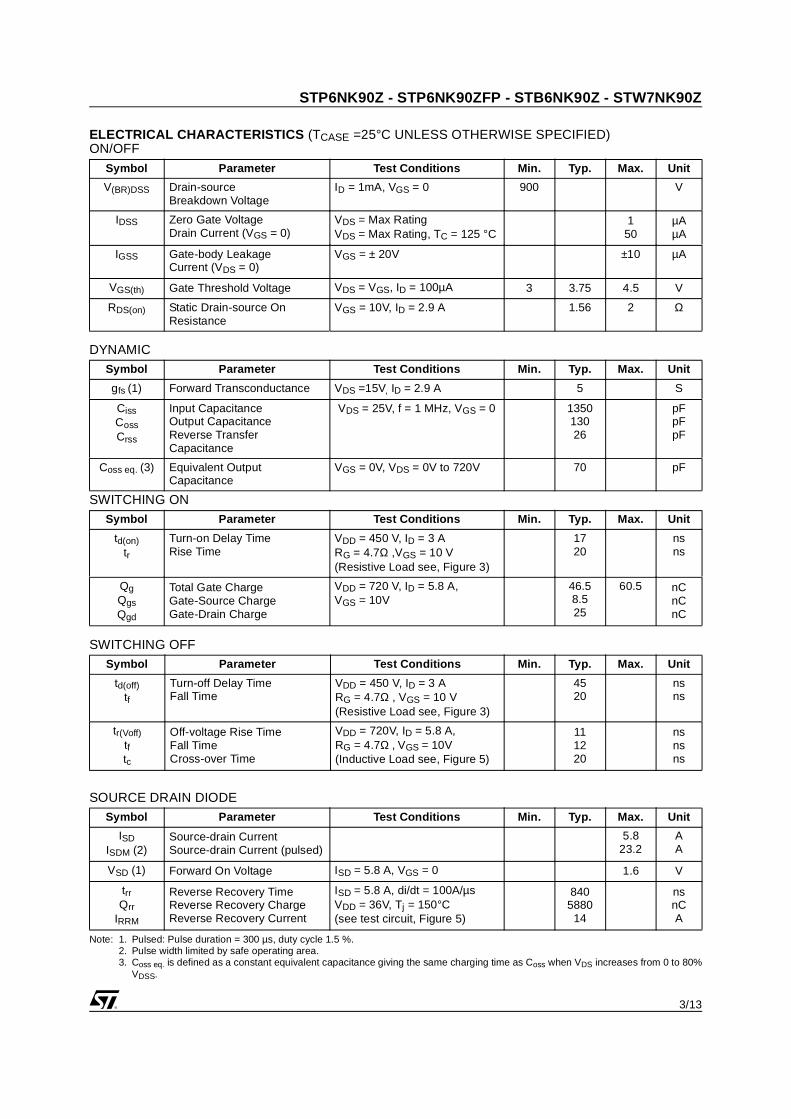
ELECTRICAL CHARACTERISTICS (TCASE =25°C UNLESS OTHERWISE SPECIFIED)ON/OFF
DYNAMIC
SWITCHING ON
SWITCHING OFF
SOURCE DRAIN DIODE
Note: 1. Pulsed: Pulse duration = 300 µs, duty cycle 1.5 %.2. Pulse width limited by safe operating area.3. Coss eq. is defined as a constant equivalent capacitance giving the same charging time as Coss when VDS increases from 0 to 80%
VDSS.
Symbol Parameter Test Conditions Min. Typ. Max. Unit
V(BR)DSS Drain-sourceBreakdown Voltage
ID = 1mA, VGS = 0 900 V
IDSS Zero Gate VoltageDrain Current (VGS = 0)
VDS = Max RatingVDS = Max Rating, TC = 125 °C
150
µAµA
IGSS Gate-body LeakageCurrent (VDS = 0)
VGS = ± 20V ±10 µA
VGS(th) Gate Threshold Voltage VDS = VGS, ID = 100µA 3 3.75 4.5 V
RDS(on) Static Drain-source OnResistance
VGS = 10V, ID = 2.9 A 1.56 2 Ω
Symbol Parameter Test Conditions Min. Typ. Max. Unit
gfs (1) Forward Transconductance VDS =15V, ID = 2.9 A 5 S
CissCossCrss
Input CapacitanceOutput CapacitanceReverse TransferCapacitance
VDS = 25V, f = 1 MHz, VGS = 0 135013026
pFpFpF
Coss eq. (3) Equivalent OutputCapacitance
VGS = 0V, VDS = 0V to 720V 70 pF
Symbol Parameter Test Conditions Min. Typ. Max. Unit
td(on)tr
Turn-on Delay TimeRise Time
VDD = 450 V, ID = 3 ARG = 4.7Ω ,VGS = 10 V(Resistive Load see, Figure 3)
1720
nsns
QgQgsQgd
Total Gate ChargeGate-Source ChargeGate-Drain Charge
VDD = 720 V, ID = 5.8 A,VGS = 10V
46.58.525
60.5 nCnCnC
Symbol Parameter Test Conditions Min. Typ. Max. Unit
td(off)tf
Turn-off Delay TimeFall Time
VDD = 450 V, ID = 3 ARG = 4.7Ω , VGS = 10 V(Resistive Load see, Figure 3)
4520
nsns
tr(Voff)tftc
Off-voltage Rise TimeFall TimeCross-over Time
VDD = 720V, ID = 5.8 A,RG = 4.7Ω , VGS = 10V(Inductive Load see, Figure 5)
111220
nsnsns
Symbol Parameter Test Conditions Min. Typ. Max. Unit
ISDISDM (2)
Source-drain CurrentSource-drain Current (pulsed)
5.823.2
AA
VSD (1) Forward On Voltage ISD = 5.8 A, VGS = 0 1.6 V
trrQrr
IRRM
Reverse Recovery TimeReverse Recovery ChargeReverse Recovery Current
ISD = 5.8 A, di/dt = 100A/µsVDD = 36V, Tj = 150°C(see test circuit, Figure 5)
8405880
14
nsnCA

STP6NK90Z - STP6NK90ZFP - STB6NK90Z - STW7NK90Z
4/13
Thermal Impedance For TO-247
Thermal Impedance For TO-220FP
Thermal Impedance For TO-220/D2PAKSafe Operating Area For TO-220/D2PAK
Safe Operating Area For TO-220FP
Safe Operating Area For TO-247
5/13
STP6NK90Z - STP6NK90ZFP - STB6NK90Z - STW7NK90Z
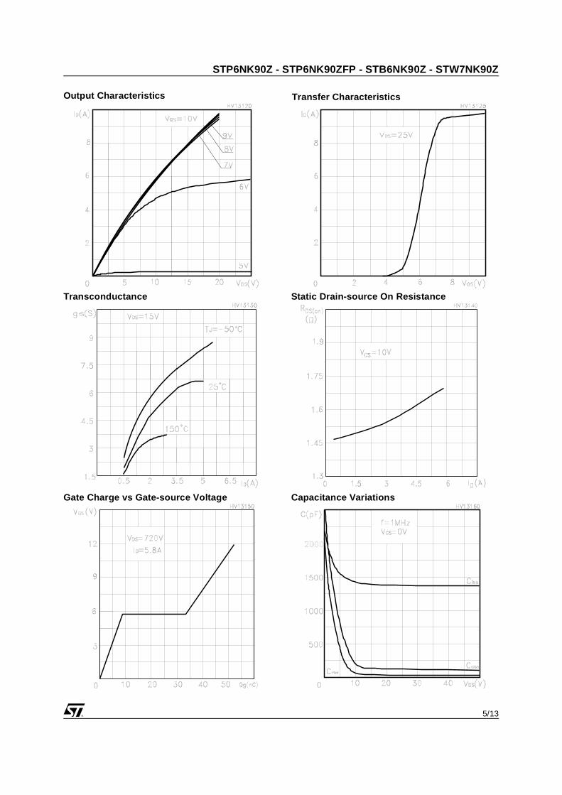
Transfer CharacteristicsOutput Characteristics
Capacitance VariationsGate Charge vs Gate-source Voltage
Static Drain-source On ResistanceTransconductance
STP6NK90Z - STP6NK90ZFP - STB6NK90Z - STW7NK90Z
6/13
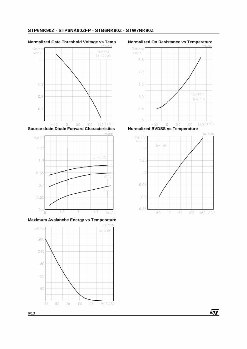
Normalized On Resistance vs TemperatureNormalized Gate Threshold Voltage vs Temp.
Maximum Avalanche Energy vs Temperature
Source-drain Diode Forward Characteristics Normalized BVDSS vs Temperature
7/13
STP6NK90Z - STP6NK90ZFP - STB6NK90Z - STW7NK90Z
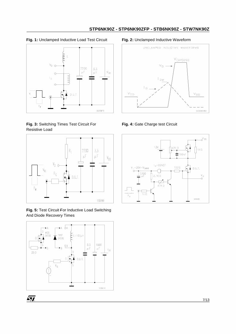
Fig. 5: Test Circuit For Inductive Load SwitchingAnd Diode Recovery Times
Fig. 4: Gate Charge test Circuit
Fig. 2: Unclamped Inductive WaveformFig. 1: Unclamped Inductive Load Test Circuit
Fig. 3: Switching Times Test Circuit ForResistive Load
STP6NK90Z - STP6NK90ZFP - STB6NK90Z - STW7NK90Z
8/13
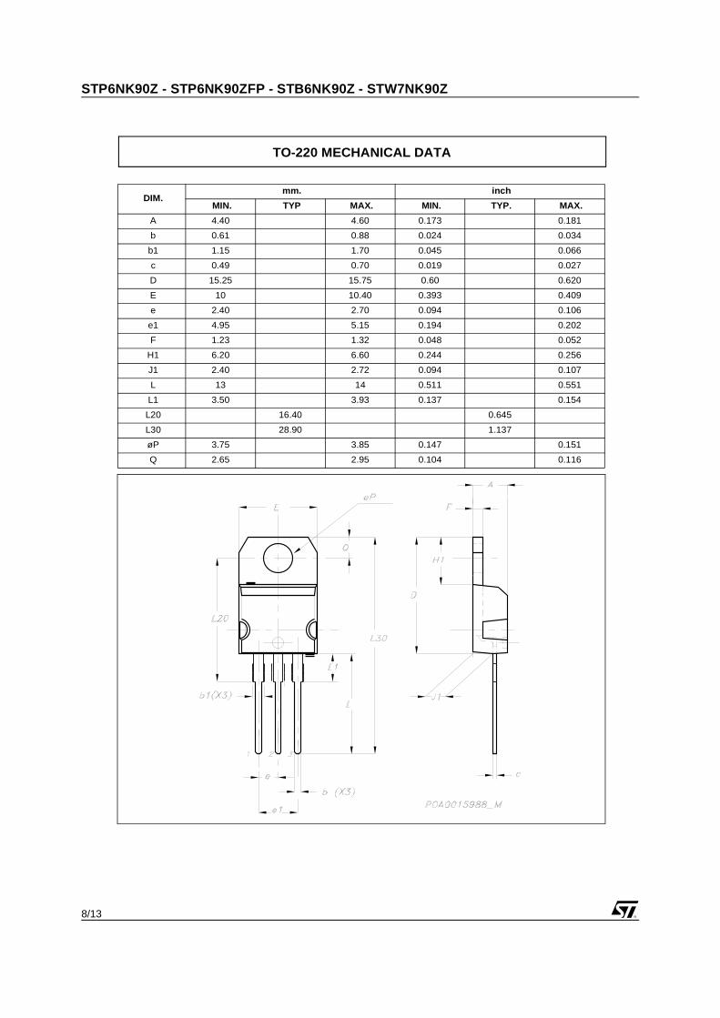
DIM.mm. inch
MIN. TYP MAX. MIN. TYP. MAX.
A 4.40 4.60 0.173 0.181
b 0.61 0.88 0.024 0.034
b1 1.15 1.70 0.045 0.066
c 0.49 0.70 0.019 0.027
D 15.25 15.75 0.60 0.620
E 10 10.40 0.393 0.409
e 2.40 2.70 0.094 0.106
e1 4.95 5.15 0.194 0.202
F 1.23 1.32 0.048 0.052
H1 6.20 6.60 0.244 0.256
J1 2.40 2.72 0.094 0.107
L 13 14 0.511 0.551
L1 3.50 3.93 0.137 0.154
L20 16.40 0.645
L30 28.90 1.137
øP 3.75 3.85 0.147 0.151
Q 2.65 2.95 0.104 0.116
TO-220 MECHANICAL DATA
9/13
STP6NK90Z - STP6NK90ZFP - STB6NK90Z - STW7NK90Z
L2
A
B
D
E
H G
L6
¯ F
L3
G1
1 2 3
F2
F1
L7
L4L5
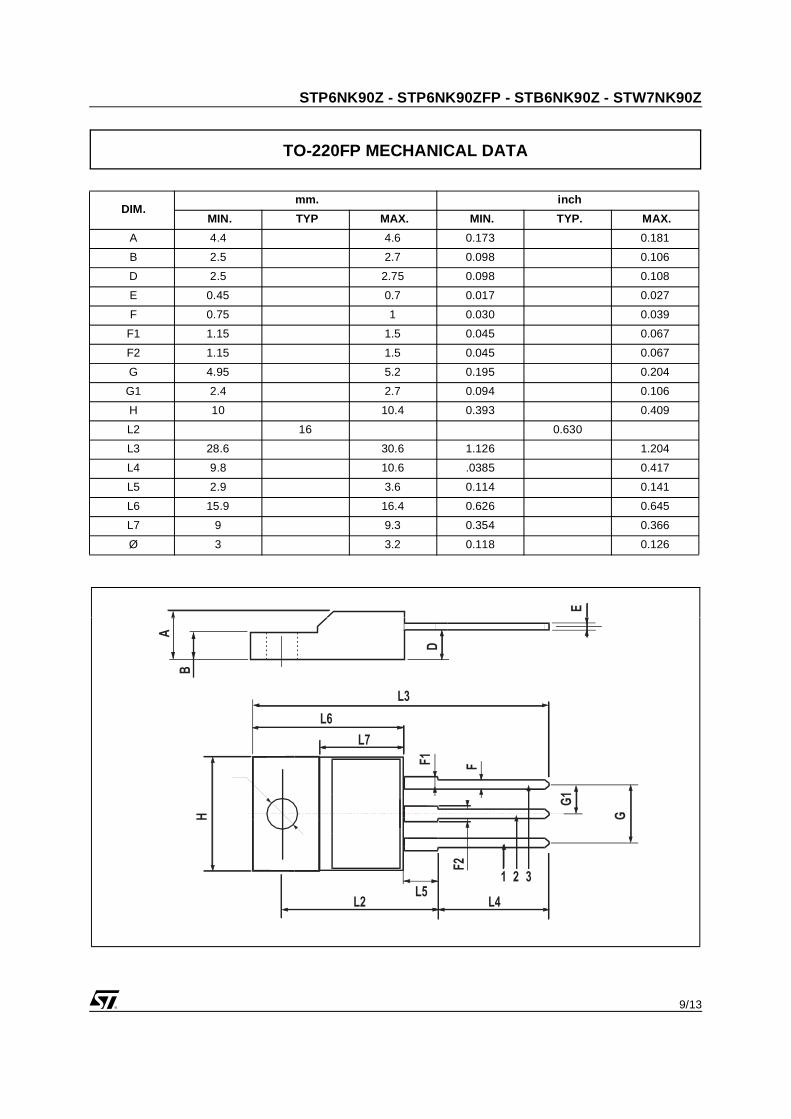
DIM.mm. inch
MIN. TYP MAX. MIN. TYP. MAX.
A 4.4 4.6 0.173 0.181
B 2.5 2.7 0.098 0.106
D 2.5 2.75 0.098 0.108
E 0.45 0.7 0.017 0.027
F 0.75 1 0.030 0.039
F1 1.15 1.5 0.045 0.067
F2 1.15 1.5 0.045 0.067
G 4.95 5.2 0.195 0.204
G1 2.4 2.7 0.094 0.106
H 10 10.4 0.393 0.409
L2 16 0.630
L3 28.6 30.6 1.126 1.204
L4 9.8 10.6 .0385 0.417
L5 2.9 3.6 0.114 0.141
L6 15.9 16.4 0.626 0.645
L7 9 9.3 0.354 0.366
Ø 3 3.2 0.118 0.126
TO-220FP MECHANICAL DATA
STP6NK90Z - STP6NK90ZFP - STB6NK90Z - STW7NK90Z
10/131
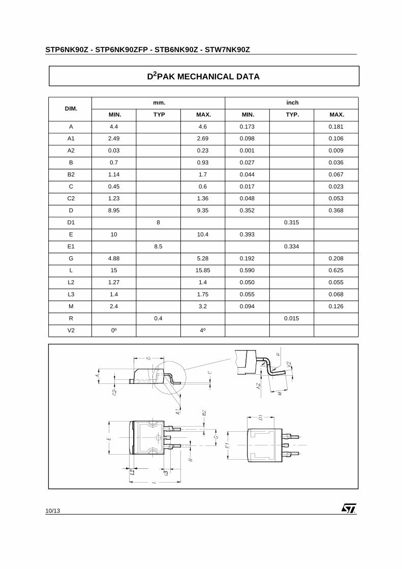
DIM.mm. inch
MIN. TYP MAX. MIN. TYP. MAX.
A 4.4 4.6 0.173 0.181
A1 2.49 2.69 0.098 0.106
A2 0.03 0.23 0.001 0.009
B 0.7 0.93 0.027 0.036
B2 1.14 1.7 0.044 0.067
C 0.45 0.6 0.017 0.023
C2 1.23 1.36 0.048 0.053
D 8.95 9.35 0.352 0.368
D1 8 0.315
E 10 10.4 0.393
E1 8.5 0.334
G 4.88 5.28 0.192 0.208
L 15 15.85 0.590 0.625
L2 1.27 1.4 0.050 0.055
L3 1.4 1.75 0.055 0.068
M 2.4 3.2 0.094 0.126
R 0.4 0.015
V2 0º 4º
D2PAK MECHANICAL DATA
3
11/13
STP6NK90Z - STP6NK90ZFP - STB6NK90Z - STW7NK90Z
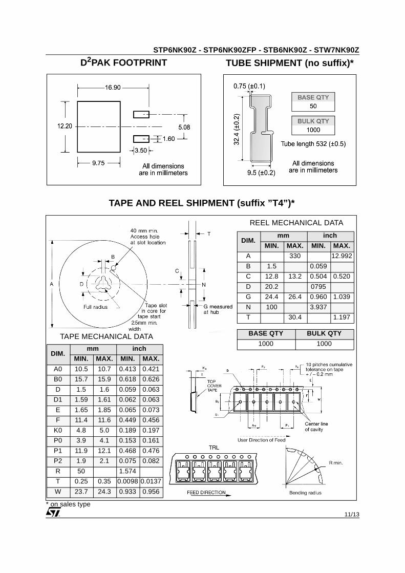
TAPE AND REEL SHIPMENT (suffix ”T4”)*
TUBE SHIPMENT (no suffix)*D2PAK FOOTPRINT
* on sales type
DIM.mm inch
MIN. MAX. MIN. MAX.
A 330 12.992
B 1.5 0.059
C 12.8 13.2 0.504 0.520
D 20.2 0795
G 24.4 26.4 0.960 1.039
N 100 3.937
T 30.4 1.197
BASE QTY BULK QTY
1000 1000
REEL MECHANICAL DATA
DIM.mm inch
MIN. MAX. MIN. MAX.
A0 10.5 10.7 0.413 0.421
B0 15.7 15.9 0.618 0.626
D 1.5 1.6 0.059 0.063
D1 1.59 1.61 0.062 0.063
E 1.65 1.85 0.065 0.073
F 11.4 11.6 0.449 0.456
K0 4.8 5.0 0.189 0.197
P0 3.9 4.1 0.153 0.161
P1 11.9 12.1 0.468 0.476
P2 1.9 2.1 0.075 0.082
R 50 1.574
T 0.25 0.35 0.0098 0.0137
W 23.7 24.3 0.933 0.956
TAPE MECHANICAL DATA
STP6NK90Z - STP6NK90ZFP - STB6NK90Z - STW7NK90Z
12/13
DIM.mm. inch
MIN. TYP MAX. MIN. TYP. MAX.
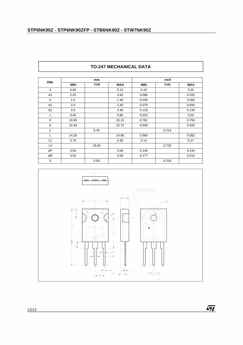
A 4.85 5.15 0.19 0.20
A1 2.20 2.60 0.086 0.102
b 1.0 1.40 0.039 0.055
b1 2.0 2.40 0.079 0.094
b2 3.0 3.40 0.118 0.134
c 0.40 0.80 0.015 0.03
D 19.85 20.15 0.781 0.793
E 15.45 15.75 0.608 0.620
e 5.45 0.214
L 14.20 14.80 0.560 0.582
L1 3.70 4.30 0.14 0.17
L2 18.50 0.728
øP 3.55 3.65 0.140 0.143
øR 4.50 5.50 0.177 0.216
S 5.50 0.216
TO-247 MECHANICAL DATA
13/13
STP6NK90Z - STP6NK90ZFP - STB6NK90Z - STW7NK90Z
Information furnished is believed to be accurate and reliable. However, STMicroelectronics assumes no responsibility for theconsequences of use of such information nor for any infringement of patents or other rights of third parties which may result f romits use. No license is granted by implication or otherwise under any patent or patent rights of STMicroelectronics. Specificati onsmentioned in this publication are subject to change without notice. This publication supersedes and replaces all informationpreviously supplied. STMicroelectronics products are not authorized for use as critical components in life support devices orsystems without express written approval of STMicroelectronics.
© The ST logo is a registered trademark of STMicroelectronics
© 2003 STMicroelectronics - Printed in Italy - All Rights ReservedSTMicroelectronics GROUP OF COMPANIES
Australia - Brazil - Canada - China - Finland - France - Germany - Hong Kong - India - Israel - Italy - Japan - Malaysia - Malta - Morocco Singapore - Spain - Sweden - Switzerland - United Kingdom - United States.
© http://www.st.com

This datasheet has been download from:
www.datasheetcatalog.com
Datasheets for electronics components.


![PR COD 1app - European Parliament · 2018-01-25 · ΑΓΡΟΤΙΚΑ ΠΡΟΪΟΝΤΑ [εκατ. ευρώ] 137 141 256 265 259 347 234 ΜΕΤΑΠΟΙΗΜΕΝΑ ΑΓΡΟΤΙΚΑ ΠΡΟΪΟΝΤΑ](https://static.fdocument.org/doc/165x107/5e5746b55b271769c56bed78/pr-cod-1app-european-2018-01-25-.jpg)