MMM5062 Technical Data Sheet - NXP Semiconductors MMM5062 is a quad-band single supply RF Power...
22
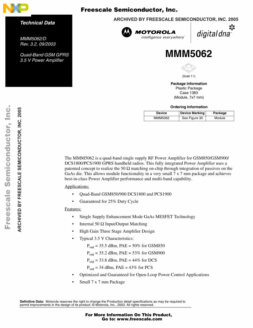
ARCHIVED BY FREESCALE SEMICONDUCTOR, INC. 2005 ARCHIVED BY FREESCALE SEMICONDUCTOR, INC. 2005 MMM5062 Ordering Information Device Device Marking Package MMM5062 See Figure 30 Module Package Information Plastic Package Case 1383 (Module, 7x7 mm) (Scale 1:1) Definitive Data: Motorola reserves the right to change the Production detail specifications as may be required to permit improvements in the design of its product. © Motorola, Inc., 2003. All rights reserved. The MMM5062 is a quad-band single supply RF Power Amplifier for GSM850/GSM900/ DCS1800/PCS1900 GPRS handheld radios. This fully integrated Power Amplifier uses a patented concept to realize the 50 Ω matching on-chip through integration of passives on the GaAs die. This allows module functionality in a very small 7 x 7 mm package and achieves best-in-class Power Amplifier performance and multi-band capability. Applications: • Quad-Band GSM850/900 DCS1800 and PCS1900 • Guaranteed for 25% Duty Cycle Features: • Single Supply Enhancement Mode GaAs MESFET Technology • Internal 50 Ω Input/Output Matching • High Gain Three Stage Amplifier Design • Typical 3.5 V Characteristics: P out = 35.5 dBm, PAE = 50% for GSM850 P out = 35.2 dBm, PAE = 53% for GSM900 P out = 33.8 dBm, PAE = 44% for DCS P out = 34 dBm, PAE = 43% for PCS • Optimized and Guaranteed for Open-Loop Power Control Applications • Small 7 x 7 mm Package Technical Data MMM5062/D Rev. 3.2, 09/2003 Quad-Band GSM GPRS 3.5 V Power Amplifier Freescale Semiconductor, I Freescale Semiconductor, Inc. For More Information On This Product, Go to: www.freescale.com nc...
Transcript of MMM5062 Technical Data Sheet - NXP Semiconductors MMM5062 is a quad-band single supply RF Power...
ARCHIVED BY FREESCALE SEMICONDUCTOR, INC. 2005A
RC
HIV
ED
BY
FR
EE
SC
AL
E S
EM
ICO
ND
UC
TOR
, IN
C. 2
005
MMM5062
Ordering Information
Device Device Marking Package
MMM5062 See Figure 30 Module
Package InformationPlastic Package
Case 1383(Module, 7x7 mm)
(Scale 1:1)
Definitive Data: Motorola reserves the right to change the Production detail specifications as may be required to permit improvements in the design of its product. © Motorola, Inc., 2003. All rights reserved.
The MMM5062 is a quad-band single supply RF Power Amplifier for GSM850/GSM900/DCS1800/PCS1900 GPRS handheld radios. This fully integrated Power Amplifier uses a patented concept to realize the 50 Ω matching on-chip through integration of passives on the GaAs die. This allows module functionality in a very small 7 x 7 mm package and achieves best-in-class Power Amplifier performance and multi-band capability.
Applications:
• Quad-Band GSM850/900 DCS1800 and PCS1900
• Guaranteed for 25% Duty Cycle
Features:
• Single Supply Enhancement Mode GaAs MESFET Technology
• Internal 50 Ω Input/Output Matching
• High Gain Three Stage Amplifier Design
• Typical 3.5 V Characteristics:
Pout = 35.5 dBm, PAE = 50% for GSM850
Pout = 35.2 dBm, PAE = 53% for GSM900
Pout = 33.8 dBm, PAE = 44% for DCS
Pout = 34 dBm, PAE = 43% for PCS
• Optimized and Guaranteed for Open-Loop Power Control Applications
• Small 7 x 7 mm Package
Technical Data
MMM5062/DRev. 3.2, 09/2003
Quad-Band GSM GPRS 3.5 V Power Amplifier
Fre
esc
ale
Se
mic
on
du
cto
r, I
Freescale Semiconductor, Inc.
For More Information On This Product, Go to: www.freescale.com
nc
...
ARCHIVED BY FREESCALE SEMICONDUCTOR, INC. 2005A
RC
HIV
ED
BY
FR
EE
SC
AL
E S
EM
ICO
ND
UC
TOR
, IN
C. 2
005
2 MMM5062 Technical Data MOTOROLA
Electrical Specifications
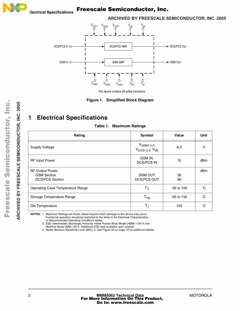
Figure 1. Simplified Block Diagram
1 Electrical SpecificationsTable 1. Maximum Ratings
Rating Symbol Value Unit
Supply VoltageVGSM1,2,3,
VDCS1,2,3, VdB6.0 V
RF Input PowerGSM IN,
DCS/PCS IN10 dBm
RF Output PowerGSM SectionDCS/PCS Section
GSM OUTDCS/PCS OUT
3836
dBm
Operating Case Temperature Range TC -35 to 100 °C
Storage Temperature Range Tstg -55 to 150 °C
Die Temperature TJ 150 °C
NOTES: 1. Maximum Ratings are those values beyond which damage to the device may occur. Functional operation should be restricted to the limits in the Electrical Characteristics or Recommended Operating Conditions tables.
2. ESD (electrostatic discharge) immunity meets Human Body Model (HBM) ≤150 V and Machine Model (MM) ≤50 V. Additional ESD data available upon request.
3. Meets Moisture Sensitivity Level (MSL) 3. See Figure 30 on page 19 for additional details.
DCS/PCS AMP
GSM AMP
DCS/PCS Out
GSM Out
DCS/PCS In
GSM In
VDCS1 Vreg
VGSM1 VBS
VapcVDCS2VDCS3
VGSM2 VGSM3VdB
This device contains 26 active transistors.
Fre
esc
ale
Se
mic
on
du
cto
r, I
Freescale Semiconductor, Inc.
For More Information On This Product, Go to: www.freescale.com
nc
...
ARCHIVED BY FREESCALE SEMICONDUCTOR, INC. 2005A
RC
HIV
ED
BY
FR
EE
SC
AL
E S
EM
ICO
ND
UC
TOR
, IN
C. 2
005
Electrical Specifications
MOTOROLA MMM5062 Technical Data 3
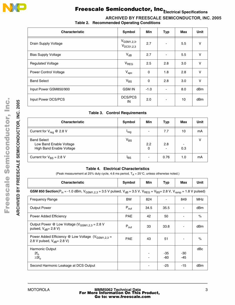
Table 2. Recommended Operating Conditions
Characteristic Symbol Min Typ Max Unit
Drain Supply VoltageVGSM1,2,3,VDCS1,2,3
2.7 - 5.5 V
Bias Supply Voltage VdB 2.7 - 5.5 V
Regulated Voltage VREG 2.5 2.8 3.0 V
Power Control Voltage Vapc 0 1.8 2.8 V
Band Select VBS 0 2.8 3.0 V
Input Power GSM850/900 GSM IN -1.0 - 8.0 dBm
Input Power DCS/PCSDCS/PCS
IN2.0 - 10 dBm
Table 3. Control Requirements
Characteristic Symbol Min Typ Max Unit
Current for Vreg @ 2.8 V Ireg - 7.7 10 mA
Band SelectLow Band Enable VoltageHigh Band Enable Voltage
VBS2.20
2.8-
-0.3
V
Current for VBS = 2.8 V IBS - 0.76 1.0 mA
Table 4. Electrical Characteristics(Peak measurement at 25% duty cycle, 4.6 ms period, TA = 25°C, unless otherwise noted.)
Characteristic Symbol Min Typ Max Unit
GSM 850 Section(Pin = -1.0 dBm, VGSM1,2,3 = 3.5 V pulsed, VdB = 3.5 V, VREG = VBS= 2.8 V, Vramp = 1.8 V pulsed)
Frequency Range BW 824 - 849 MHz
Output Power Pout 34.5 35.5 - dBm
Power Added Efficiency PAE 42 50 - %
Output Power @ Low Voltage (VGSM1,2,3 = 2.8 V pulsed, VdB= 2.8 V)
Pout 33 33.8 - dBm
Power Added Efficiency @ Low Voltage (VGSM1,2,3 = 2.8 V pulsed, VdB= 2.8 V)
PAE 43 51 - %
Harmonic Output2fo≥3fo
--
-35-60
-30-45
dBc
Second Harmonic Leakage at DCS Output - -25 -15 dBm
Fre
esc
ale
Se
mic
on
du
cto
r, I
Freescale Semiconductor, Inc.
For More Information On This Product, Go to: www.freescale.com
nc
...
ARCHIVED BY FREESCALE SEMICONDUCTOR, INC. 2005A
RC
HIV
ED
BY
FR
EE
SC
AL
E S
EM
ICO
ND
UC
TOR
, IN
C. 2
005
4 MMM5062 Technical Data MOTOROLA
Electrical Specifications
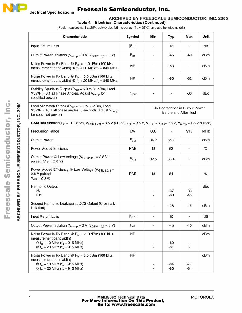
Input Return Loss |S11| - 13 - dB
Output Power Isolation (Vramp = 0 V, VGSM1,2,3 = 0 V) Poff - -45 -40 dBm
Noise Power in Rx Band @ Pin = -1.0 dBm (100 kHz measurement bandwidth) @ fo + 20 MHz fo = 849 MHz
NP - -83 - dBm
Noise Power in Rx Band @ Pin = 6.0 dBm (100 kHz measurement bandwidth) @ fo + 20 MHz fo = 849 MHz
NP - -86 -82 dBm
Stability-Spurious Output (Pout = 5.0 to 35 dBm, Load VSWR = 6:1 all Phase Angles, Adjust Vramp for specified power)
Pspur - - -60 dBc
Load Mismatch Stress (Pout = 5.0 to 35 dBm, Load VSWR = 10:1 all phase angles, 5 seconds, Adjust Vramp for specified power)
No Degradation in Output PowerBefore and After Test
GSM 900 Section(Pin = -1.0 dBm, VGSM1,2,3 = 3.5 V pulsed, VdB = 3.5 V, VREG = VBS= 2.8 V, Vramp = 1.8 V pulsed)
Frequency Range BW 880 - 915 MHz
Output Power Pout 34.2 35.2 - dBm
Power Added Efficiency PAE 48 53 - %
Output Power @ Low Voltage (VGSM1,2,3 = 2.8 V pulsed, VdB = 2.8 V)
Pout 32.5 33.4 - dBm
Power Added Efficiency @ Low Voltage (VGSM1,2,3 = 2.8 V pulsed,VdB = 2.8 V)
PAE 48 54 - %
Harmonic Output2fo≥3fo
--
-37-60
-33-45
dBc
Second Harmonic Leakage at DCS Output (Crosstalk isolation)
- -28 -15 dBm
Input Return Loss |S11| - 10 - dB
Output Power Isolation (Vramp = 0 V, VGSM1,2,3 = 0 V) Poff - -45 -40 dBm
Noise Power in Rx Band @ Pin = -1.0 dBm (100 kHz measurement bandwidth)
@ fo + 10 MHz (fo = 915 MHz)@ fo + 20 MHz (fo = 915 MHz)
NP
--
-80-81
--
dBm
Noise Power in Rx Band @ Pin = 6.0 dBm (100 kHz measurement bandwidth)
@ fo + 10 MHz (fo = 915 MHz)@ fo + 20 MHz (fo = 915 MHz)
NP
--
-84-86
-77-81
dBm
Table 4. Electrical Characteristics (Continued)(Peak measurement at 25% duty cycle, 4.6 ms period, TA = 25°C, unless otherwise noted.)
Characteristic Symbol Min Typ Max Unit
Fre
esc
ale
Se
mic
on
du
cto
r, I
Freescale Semiconductor, Inc.
For More Information On This Product, Go to: www.freescale.com
nc
...
ARCHIVED BY FREESCALE SEMICONDUCTOR, INC. 2005A
RC
HIV
ED
BY
FR
EE
SC
AL
E S
EM
ICO
ND
UC
TOR
, IN
C. 2
005
Electrical Specifications
MOTOROLA MMM5062 Technical Data 5
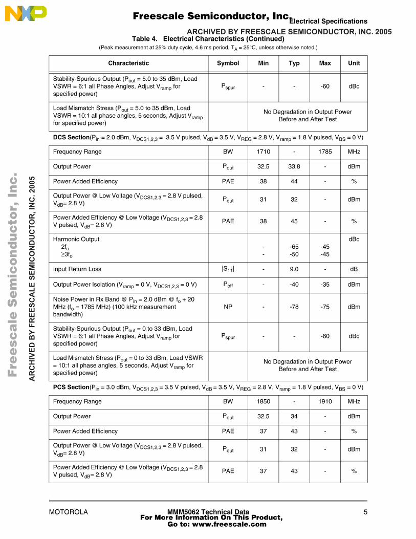
Stability-Spurious Output (Pout = 5.0 to 35 dBm, Load VSWR = 6:1 all Phase Angles, Adjust Vramp for specified power)
Pspur - - -60 dBc
Load Mismatch Stress (Pout = 5.0 to 35 dBm, Load VSWR = 10:1 all phase angles, 5 seconds, Adjust Vramp for specified power)
No Degradation in Output PowerBefore and After Test
DCS Section(Pin = 2.0 dBm, VDCS1,2,3 = 3.5 V pulsed, VdB = 3.5 V, VREG = 2.8 V, Vramp = 1.8 V pulsed, VBS = 0 V)
Frequency Range BW 1710 - 1785 MHz
Output Power Pout 32.5 33.8 - dBm
Power Added Efficiency PAE 38 44 - %
Output Power @ Low Voltage (VDCS1,2,3 = 2.8 V pulsed, VdB= 2.8 V)
Pout 31 32 - dBm
Power Added Efficiency @ Low Voltage (VDCS1,2,3 = 2.8 V pulsed, VdB= 2.8 V)
PAE 38 45 - %
Harmonic Output2fo≥3fo
--
-65-50
-45-45
dBc
Input Return Loss |S11| - 9.0 - dB
Output Power Isolation (Vramp = 0 V, VDCS1,2,3 = 0 V) Poff - -40 -35 dBm
Noise Power in Rx Band @ Pin = 2.0 dBm @ fo + 20 MHz (fo = 1785 MHz) (100 kHz measurement bandwidth)
NP - -78 -75 dBm
Stability-Spurious Output (Pout = 0 to 33 dBm, Load VSWR = 6:1 all Phase Angles, Adjust Vramp for specified power)
Pspur - - -60 dBc
Load Mismatch Stress (Pout = 0 to 33 dBm, Load VSWR = 10:1 all phase angles, 5 seconds, Adjust Vramp for specified power)
No Degradation in Output PowerBefore and After Test
PCS Section(Pin = 3.0 dBm, VDCS1,2,3 = 3.5 V pulsed, VdB = 3.5 V, VREG = 2.8 V, Vramp = 1.8 V pulsed, VBS = 0 V)
Frequency Range BW 1850 - 1910 MHz
Output Power Pout 32.5 34 - dBm
Power Added Efficiency PAE 37 43 - %
Output Power @ Low Voltage (VDCS1,2,3 = 2.8 V pulsed, VdB= 2.8 V)
Pout 31 32 - dBm
Power Added Efficiency @ Low Voltage (VDCS1,2,3 = 2.8 V pulsed, VdB= 2.8 V)
PAE 37 43 - %
Table 4. Electrical Characteristics (Continued)(Peak measurement at 25% duty cycle, 4.6 ms period, TA = 25°C, unless otherwise noted.)
Characteristic Symbol Min Typ Max Unit
Fre
esc
ale
Se
mic
on
du
cto
r, I
Freescale Semiconductor, Inc.
For More Information On This Product, Go to: www.freescale.com
nc
...
ARCHIVED BY FREESCALE SEMICONDUCTOR, INC. 2005A
RC
HIV
ED
BY
FR
EE
SC
AL
E S
EM
ICO
ND
UC
TOR
, IN
C. 2
005
6 MMM5062 Technical Data MOTOROLA
Electrical Specifications
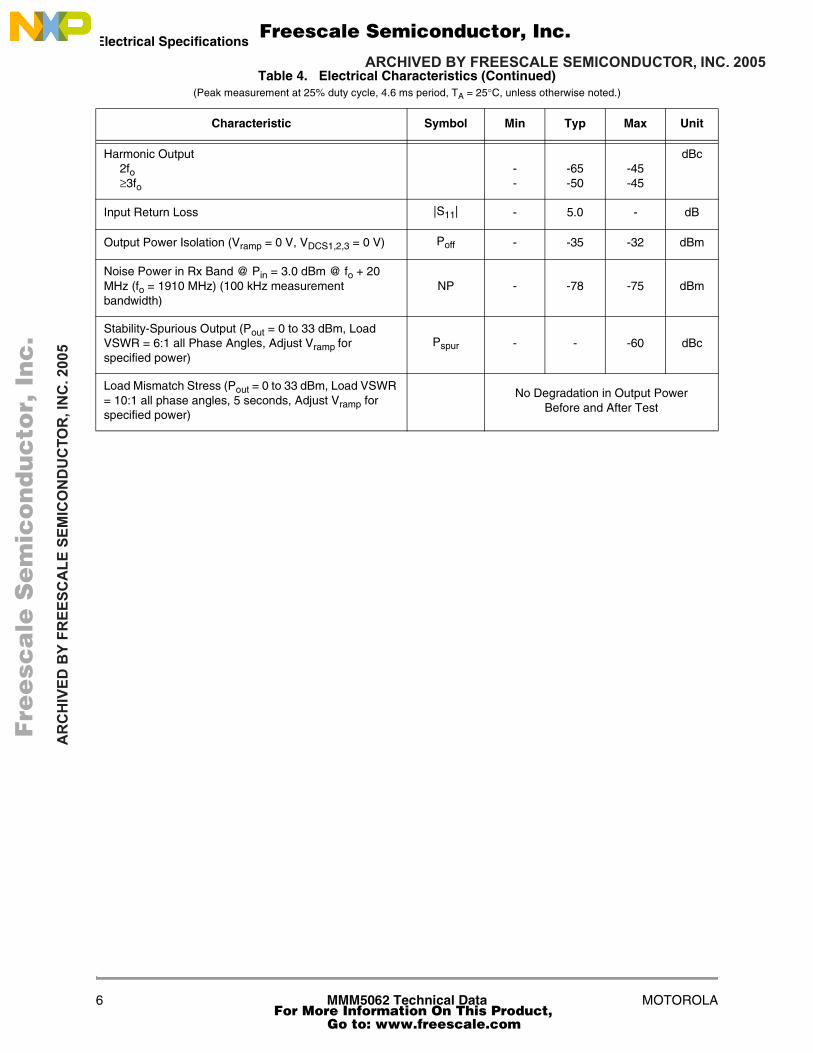
Harmonic Output2fo≥3fo
--
-65-50
-45-45
dBc
Input Return Loss |S11| - 5.0 - dB
Output Power Isolation (Vramp = 0 V, VDCS1,2,3 = 0 V) Poff - -35 -32 dBm
Noise Power in Rx Band @ Pin = 3.0 dBm @ fo + 20 MHz (fo = 1910 MHz) (100 kHz measurement bandwidth)
NP - -78 -75 dBm
Stability-Spurious Output (Pout = 0 to 33 dBm, Load VSWR = 6:1 all Phase Angles, Adjust Vramp for specified power)
Pspur - - -60 dBc
Load Mismatch Stress (Pout = 0 to 33 dBm, Load VSWR = 10:1 all phase angles, 5 seconds, Adjust Vramp for specified power)
No Degradation in Output PowerBefore and After Test
Table 4. Electrical Characteristics (Continued)(Peak measurement at 25% duty cycle, 4.6 ms period, TA = 25°C, unless otherwise noted.)
Characteristic Symbol Min Typ Max Unit
Fre
esc
ale
Se
mic
on
du
cto
r, I
Freescale Semiconductor, Inc.
For More Information On This Product, Go to: www.freescale.com
nc
...

ARCHIVED BY FREESCALE SEMICONDUCTOR, INC. 2005A
RC
HIV
ED
BY
FR
EE
SC
AL
E S
EM
ICO
ND
UC
TOR
, IN
C. 2
005
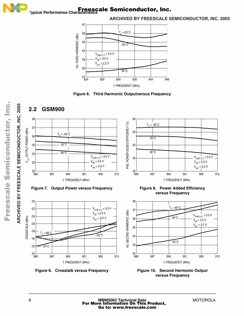
Typical Performance Characteristics
MOTOROLA MMM5062 Technical Data 7
2 Typical Performance Characteristics
2.1 GSM850
Figure 2. Output Power versus Frequency Figure 3. Power Added Efficiencyversus Frequency
Figure 4. Crosstalk versus Frequency Figure 5. Second Harmonic Outputversus Frequency
38
824
f, FREQUENCY (MHz)
P out, O
UTP
UT
POW
ER (d
Bm)
829 834 839 844 849
37
36
35
34
33
32
VGSM1,2,3 = 3.5 V
VdB = 3.5 V
Vapc = 2.2 V
25°C
TA = -35°C
85°C
56
824
f, FREQUENCY (MHz)
PAE,
PO
WER
AD
DED
EFF
ICIE
NC
Y (%
)
829 834 839 844 849
54
52
50
48
46
44
VGSM1,2,3 = 3.5 V
VdB = 3.5 V
Vapc = 2.2 V
25°C
TA = -35°C
85°C
-10
824
f, FREQUENCY (MHz)
CR
OSS
TALK
(dBm
)
829 834 839 844 849
-15
-20
-25
-30
-35
VGSM1,2,3 = 3.5 V
VdB = 3.5 V
Vapc = 2.2 V
25°C
TA = -35°C
85°C
38
824
f, FREQUENCY (MHz)
H2,
SEC
ON
D H
ARM
ON
IC (d
Bc)
829 834 839 844 849
37
36
35
34
32
VGSM1,2,3 = 3.5 V
VdB = 3.5 V
Vapc = 2.2 V
25°C
TA = 85°C
-35°C33
Fre
esc
ale
Se
mic
on
du
cto
r, I
Freescale Semiconductor, Inc.
For More Information On This Product, Go to: www.freescale.com
nc
...
ARCHIVED BY FREESCALE SEMICONDUCTOR, INC. 2005A
RC
HIV
ED
BY
FR
EE
SC
AL
E S
EM
ICO
ND
UC
TOR
, IN
C. 2
005
8 MMM5062 Technical Data MOTOROLA
Typical Performance Characteristics
2.2 GSM900
Figure 6. Third Harmonic Outputversus Frequency
Figure 7. Output Power versus Frequency Figure 8. Power Added Efficiencyversus Frequency
Figure 9. Crosstalk versus Frequency Figure 10. Second Harmonic Outputversus Frequency
67
824
f, FREQUENCY (MHz)
H3,
TH
IRD
HAR
MO
NIC
(dBc
)829 834 839 844 849
66
65
64
63
61
VGSM1,2,3 = 3.5 V
VdB = 3.5 V
Vapc = 2.2 V
-35°C
TA = 25°C
85°C62
38
880
f, FREQUENCY (MHz)
P out, O
UTP
UT
POW
ER (d
Bm)
887 894 901 908 915
37
36
35
34
33
32
VGSM1,2,3 = 3.5 V
VdB = 3.5 V
Vapc = 2.2 V
25°C
TA = -35°C
85°C
60
880
f, FREQUENCY (MHz)
PAE,
PO
WER
AD
DED
EFF
ICIE
NC
Y (%
)
887 894 901 908 915
55
50
45
40
VGSM1,2,3 = 3.5 V
VdB = 3.5 V
Vapc = 2.2 V
25°C
TA = -35°C
85°C
-20
880
f, FREQUENCY (MHz)
CR
OSS
TALK
(dBm
)
887 894 901 908 915
-22
-28
-30
-32
-34
VGSM1,2,3 = 3.5 V
VdB = 3.5 V
Vapc = 2.2 V
25°C
TA = 85°C-35°C
-26
-24
38
880
f, FREQUENCY (MHz)
H2,
SEC
ON
D H
ARM
ON
IC (d
Bc)
887 894 901 908 915
37
36
35
34
32
VGSM1,2,3 = 3.5 V
VdB = 3.5 V
Vapc = 2.2 V
25°C
TA = 85°C
-35°C33
Fre
esc
ale
Se
mic
on
du
cto
r, I
Freescale Semiconductor, Inc.
For More Information On This Product, Go to: www.freescale.com
nc
...
ARCHIVED BY FREESCALE SEMICONDUCTOR, INC. 2005A
RC
HIV
ED
BY
FR
EE
SC
AL
E S
EM
ICO
ND
UC
TOR
, IN
C. 2
005
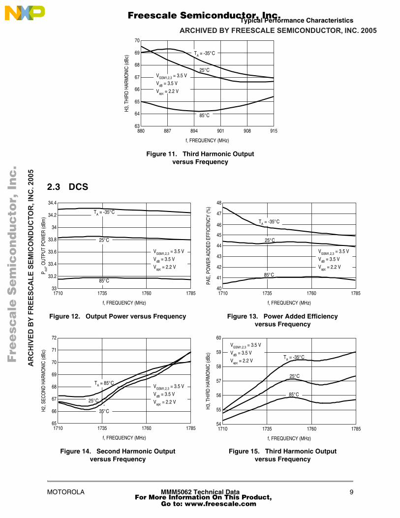
Typical Performance Characteristics
MOTOROLA MMM5062 Technical Data 9
2.3 DCS
Figure 11. Third Harmonic Outputversus Frequency
Figure 12. Output Power versus Frequency Figure 13. Power Added Efficiencyversus Frequency
Figure 14. Second Harmonic Outputversus Frequency
Figure 15. Third Harmonic Outputversus Frequency
70
880
f, FREQUENCY (MHz)
H3,
TH
IRD
HAR
MO
NIC
(dBc
)887 894 901 908 915
69
67
66
65
63
VGSM1,2,3 = 3.5 V
VdB = 3.5 V
Vapc = 2.2 V
25°C
TA = -35°C
85°C64
68
34.4
1710
f, FREQUENCY (MHz)
P out, O
UTP
UT
POW
ER (d
Bm)
1735 1760 1785
34
33.8
33.6
33.4
33.2
33
VGSM1,2,3 = 3.5 V
VdB = 3.5 V
Vapc = 2.2 V
25°C
TA = -35°C
85°C
34.2
48
1710
f, FREQUENCY (MHz)
PAE,
PO
WER
AD
DED
EFF
ICIE
NC
Y (%
)
1735 1760 1785
45
44
43
42
41
40
VGSM1,2,3 = 3.5 V
VdB = 3.5 V
Vapc = 2.2 V
25°C
TA = -35°C
85°C
47
46
VGSM1,2,3 = 3.5 V
VdB = 3.5 V
Vapc = 2.2 V
72
1710
f, FREQUENCY (MHz)
H2,
SEC
ON
D H
ARM
ON
IC (d
Bc)
1735 1760 1785
70
69
68
67
66
65
25°C
TA = 85°C
-35°C
71VGSM1,2,3 = 3.5 V
VdB = 3.5 V
Vapc = 2.2 V
60
1710
f, FREQUENCY (MHz)
H3,
TH
IRD
HAR
MO
NIC
(dBc
)
1735 1760 1785
58
57
56
55
54
25°C
TA = -35°C
85°C
59
Fre
esc
ale
Se
mic
on
du
cto
r, I
Freescale Semiconductor, Inc.
For More Information On This Product, Go to: www.freescale.com
nc
...
ARCHIVED BY FREESCALE SEMICONDUCTOR, INC. 2005A
RC
HIV
ED
BY
FR
EE
SC
AL
E S
EM
ICO
ND
UC
TOR
, IN
C. 2
005
10 MMM5062 Technical Data MOTOROLA
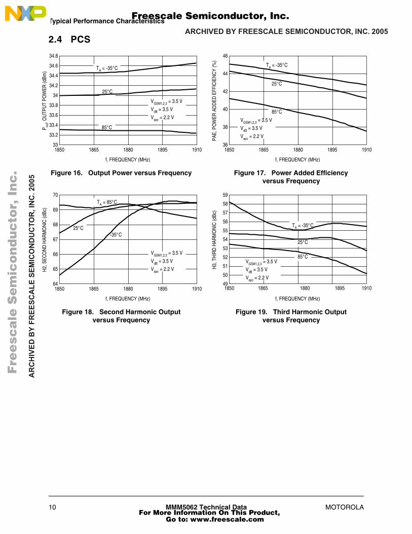
Typical Performance Characteristics
2.4 PCS
Figure 16. Output Power versus Frequency Figure 17. Power Added Efficiencyversus Frequency
Figure 18. Second Harmonic Outputversus Frequency
Figure 19. Third Harmonic Outputversus Frequency
34.8
1850
f, FREQUENCY (MHz)
P out, O
UTP
UT
POW
ER (d
Bm)
1865 1895 1910
34.2
33.8
33.6
33.4
33.2
33
VGSM1,2,3 = 3.5 V
VdB = 3.5 V
Vapc = 2.2 V
25°C
TA = -35°C
85°C
34.6
1880
34
34.4
46
1850
f, FREQUENCY (MHz)
PAE,
PO
WER
AD
DED
EFF
ICIE
NC
Y (%
)
1865 1880 1910
44
42
40
38
36
VGSM1,2,3 = 3.5 V
VdB = 3.5 V
Vapc = 2.2 V
25°C
TA = -35°C
85°C
1895
VGSM1,2,3 = 3.5 V
VdB = 3.5 V
Vapc = 2.2 V
70
1850
f, FREQUENCY (MHz)
H2,
SEC
ON
D H
ARM
ON
IC (d
Bc)
1865 1880 1910
69
68
67
66
65
64
25°C
TA = 85°C
-35°C
1895
VGSM1,2,3 = 3.5 V
VdB = 3.5 V
Vapc = 2.2 V
59
1850
f, FREQUENCY (MHz)
H3,
TH
IRD
HAR
MO
NIC
(dBc
)
1865 1880 1910
53
52
51
50
49
25°C
TA = -35°C
85°C
54
1895
55
56
57
58
Fre
esc
ale
Se
mic
on
du
cto
r, I
Freescale Semiconductor, Inc.
For More Information On This Product, Go to: www.freescale.com
nc
...
ARCHIVED BY FREESCALE SEMICONDUCTOR, INC. 2005A
RC
HIV
ED
BY
FR
EE
SC
AL
E S
EM
ICO
ND
UC
TOR
, IN
C. 2
005
Pin Descriptions and Connections
MOTOROLA MMM5062 Technical Data 11
3 Pin Descriptions and Connections
Figure 20. Pin Connections(Bottom View)
Table 5. Pin Function Description
Pin Symbol Description
1 Vreg Regulated dc voltage for bias circuit
2 VdB DC supply voltage for active bias circuits connected to the battery
3 DCS/PCS Out DCS/PCS RF output
4 VDCS3 DCS/PCS DC supply voltage for 3rd stage
5 VDCS2 DCS/PCS DC supply voltage for 2nd stage
6 VDCS1 DCS/PCS DC supply voltage for 1st stage
7 Vapc Power control for both line-ups (Vapc = 0 V, Pout = Poff, Vapc = 1.8 V, Pout = Pmax)
8 DCS/PCS In DCS/PCS RF input
9 GSM In GSM850/GSM900 RF input
10 VGSM1 GSM850/GSM900 DC supply voltage for 1st stage
11 VGSM2 GSM850/GSM900 DC supply voltage for 2nd stage
12 VGSM3 GSM850/GSM900 DC supply voltage for 3rd stage
13 GSM Out GSM850/GSM900 RF output
14 VBS Band selection between GSM850/GSM900 and DCS/PCS
DCS/PCS OutVdBVreg
VBS
GSM Out
VGSM3 VGSM2 VGSM1 GSM In
DCS/PCS In
Vramp
VDCS1
VDCS2
VDCS3
Ground Plane
(0.95)
(0.60)
Pin 1 Pad Corner
NOTE: For optimum performance VGSM1 and VGSM2, as well as VDCS1 and VDCS2, must be strapped together on the application demobard.
Fre
esc
ale
Se
mic
on
du
cto
r, I
Freescale Semiconductor, Inc.
For More Information On This Product, Go to: www.freescale.com
nc
...
ARCHIVED BY FREESCALE SEMICONDUCTOR, INC. 2005A
RC
HIV
ED
BY
FR
EE
SC
AL
E S
EM
ICO
ND
UC
TOR
, IN
C. 2
005
12 MMM5062 Technical Data MOTOROLA
Application Information
4 Application Information
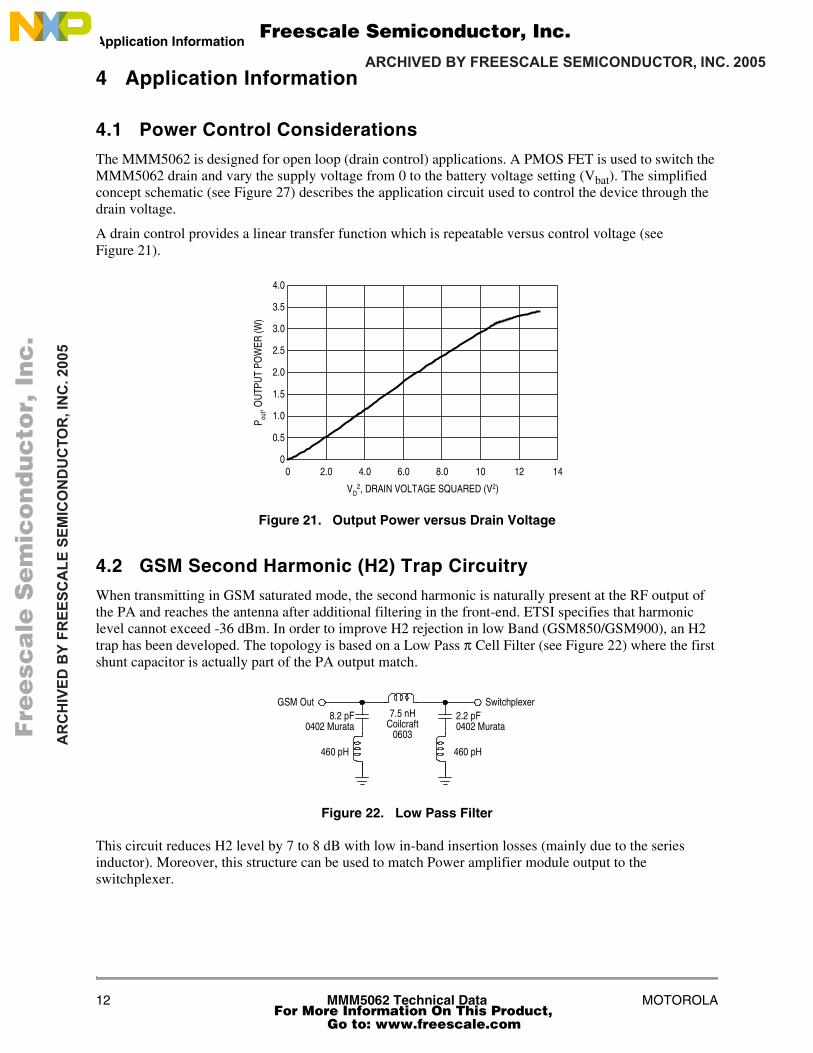
4.1 Power Control Considerations
The MMM5062 is designed for open loop (drain control) applications. A PMOS FET is used to switch the MMM5062 drain and vary the supply voltage from 0 to the battery voltage setting (Vbat). The simplified concept schematic (see Figure 27) describes the application circuit used to control the device through the drain voltage.
A drain control provides a linear transfer function which is repeatable versus control voltage (see Figure 21).
Figure 21. Output Power versus Drain Voltage
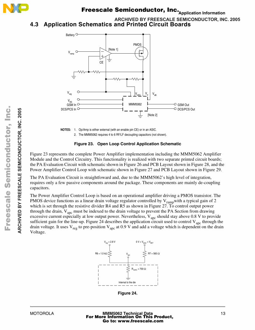
4.2 GSM Second Harmonic (H2) Trap Circuitry
When transmitting in GSM saturated mode, the second harmonic is naturally present at the RF output of the PA and reaches the antenna after additional filtering in the front-end. ETSI specifies that harmonic level cannot exceed -36 dBm. In order to improve H2 rejection in low Band (GSM850/GSM900), an H2 trap has been developed. The topology is based on a Low Pass π Cell Filter (see Figure 22) where the first shunt capacitor is actually part of the PA output match.
Figure 22. Low Pass Filter
This circuit reduces H2 level by 7 to 8 dB with low in-band insertion losses (mainly due to the series inductor). Moreover, this structure can be used to match Power amplifier module output to the switchplexer.
4.0
0
VD2, DRAIN VOLTAGE SQUARED (V2)
P out, O
UTP
UT
POW
ER (W
)
2.0 4.0 6.0 8.0 10 12 14
3.5
3.0
2.5
2.0
1.5
1.0
0.5
0
7.5 nHCoilcraft
0603
8.2 pF0402 Murata
460 pH
2.2 pF0402 Murata
460 pH
SwitchplexerGSM Out
Fre
esc
ale
Se
mic
on
du
cto
r, I
Freescale Semiconductor, Inc.
For More Information On This Product, Go to: www.freescale.com
nc
...
ARCHIVED BY FREESCALE SEMICONDUCTOR, INC. 2005A
RC
HIV
ED
BY
FR
EE
SC
AL
E S
EM
ICO
ND
UC
TOR
, IN
C. 2
005
Application Information
MOTOROLA MMM5062 Technical Data 13
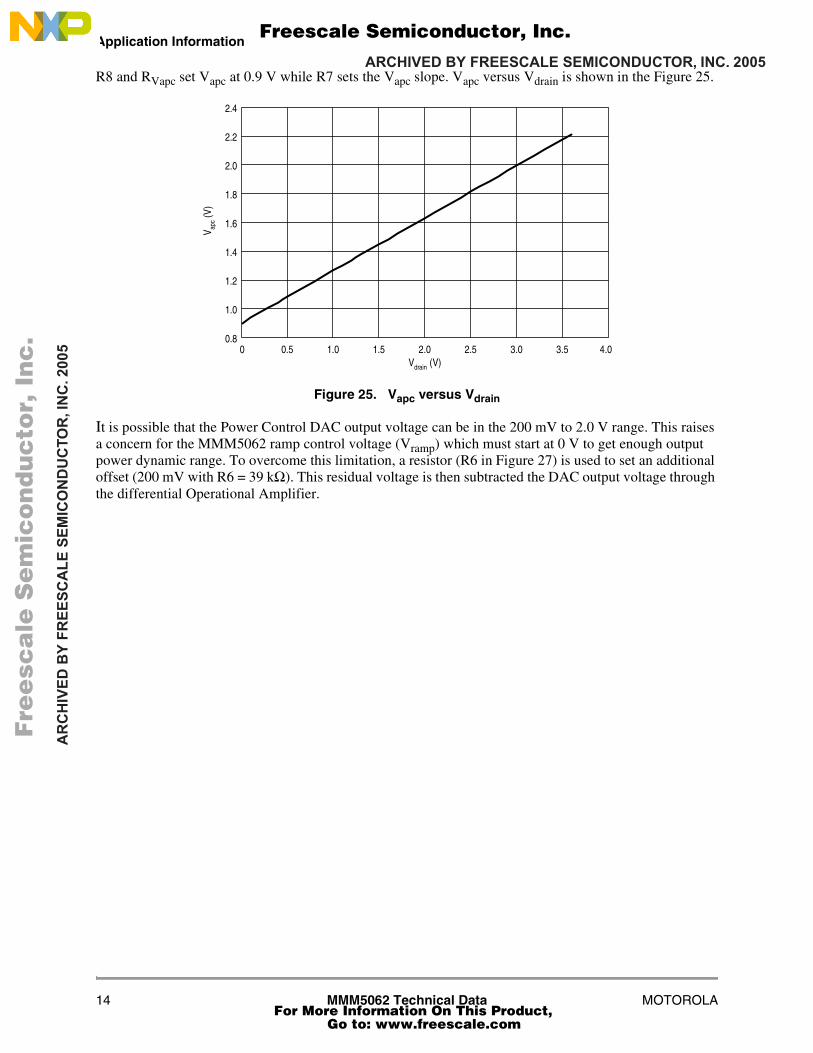
4.3 Application Schematics and Printed Circuit Boards
Figure 23. Open Loop Control Application Schematic
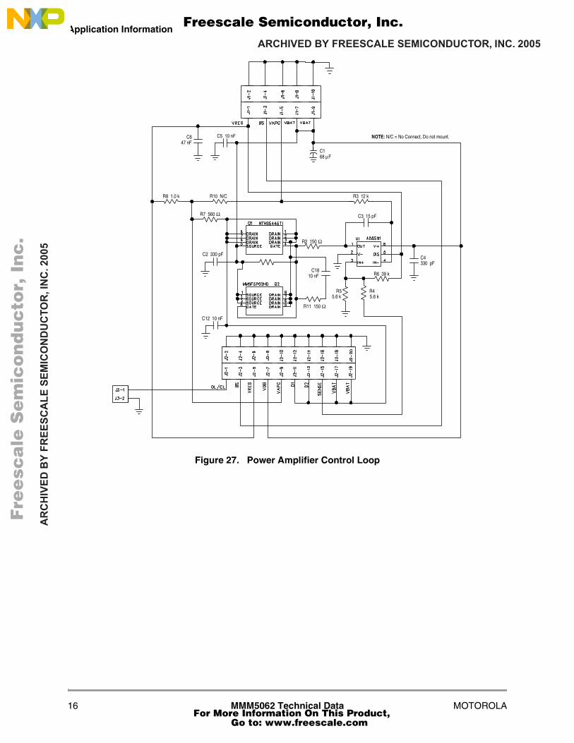
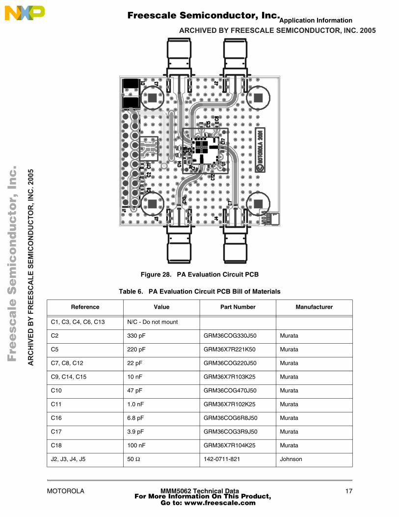
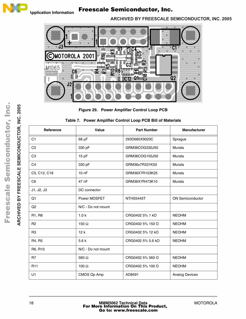
Figure 23 represents the complete Power Amplifier implementation including the MMM5062 Amplifier Module and the Control Circuitry. This functionality is realized with two separate printed circuit boards; the PA Evaluation Circuit with schematic shown in Figure 26 and PCB Layout shown in Figure 28, and the Power Amplifier Control Loop with schematic shown in Figure 27 and PCB Layout shown in Figure 29.
The PA Evaluation Circuit is straightfoward and, due to the MMM5062’s high level of integration, requires only a few passive components around the package. These components are mainly de-coupling capacitors.
The Power Amplifier Control Loop is based on an operational amplifier driving a PMOS transistor. The PMOS device functions as a linear drain voltage regulator controlled by Vrampwith a typical gain of 2 which is set through the resistive divider R4 and R5 as shown in Figure 27. To control output power through the drain, Vapc must be indexed to the drain voltage to prevent the PA Section from drawing excessive current especially at low output power. Nevertheless, Vapc should stay above 0.8 V to provide sufficient gain for the line-up. Figure 24 describes the application circuit used to control Vapc through the drain voltage. It uses Vreg to pre-position Vapc at 0.9 V and add a voltage which is dependent on the drain Voltage.
Figure 24.
GSM OutDCS/PCS Out
MMM5062
VdBVdVAPC
CE
PMOS[Note 1]
Battery
Vramp
Vreg
VBS
GSM InDCS/PCS In
[Note 2]
NOTES: 1. Op/Amp is either external (with an enable pin CE) or in an ASIC.
2. The MMM5062 requires 4 to 6 RF/LF decoupling capacitors (not shown).
Vreg = 2.8 V 0 V < Vdrain < VBAT
VapcR7 = 560 ΩR8 = 1.0 kΩ
RVAPC = 700 Ω
Internal to the die
Fre
esc
ale
Se
mic
on
du
cto
r, I
Freescale Semiconductor, Inc.
For More Information On This Product, Go to: www.freescale.com
nc
...
ARCHIVED BY FREESCALE SEMICONDUCTOR, INC. 2005A
RC
HIV
ED
BY
FR
EE
SC
AL
E S
EM
ICO
ND
UC
TOR
, IN
C. 2
005
14 MMM5062 Technical Data MOTOROLA
Application Information
R8 and RVapc set Vapc at 0.9 V while R7 sets the Vapc slope. Vapc versus Vdrain is shown in the Figure 25.
Figure 25. Vapc versus Vdrain
It is possible that the Power Control DAC output voltage can be in the 200 mV to 2.0 V range. This raises a concern for the MMM5062 ramp control voltage (Vramp) which must start at 0 V to get enough output power dynamic range. To overcome this limitation, a resistor (R6 in Figure 27) is used to set an additional offset (200 mV with R6 = 39 kΩ). This residual voltage is then subtracted the DAC output voltage through the differential Operational Amplifier.
0.8
1.0
1.2
1.4
1.6
1.8
2.0
2.2
2.4
0 0.5 1.0 1.5 2.0 2.5 3.0 3.5 4.0Vdrain (V)
V apc (V
)
Fre
esc
ale
Se
mic
on
du
cto
r, I
Freescale Semiconductor, Inc.
For More Information On This Product, Go to: www.freescale.com
nc
...
ARCHIVED BY FREESCALE SEMICONDUCTOR, INC. 2005A
RC
HIV
ED
BY
FR
EE
SC
AL
E S
EM
ICO
ND
UC
TOR
, IN
C. 2
005
Application Information
MOTOROLA MMM5062 Technical Data 15
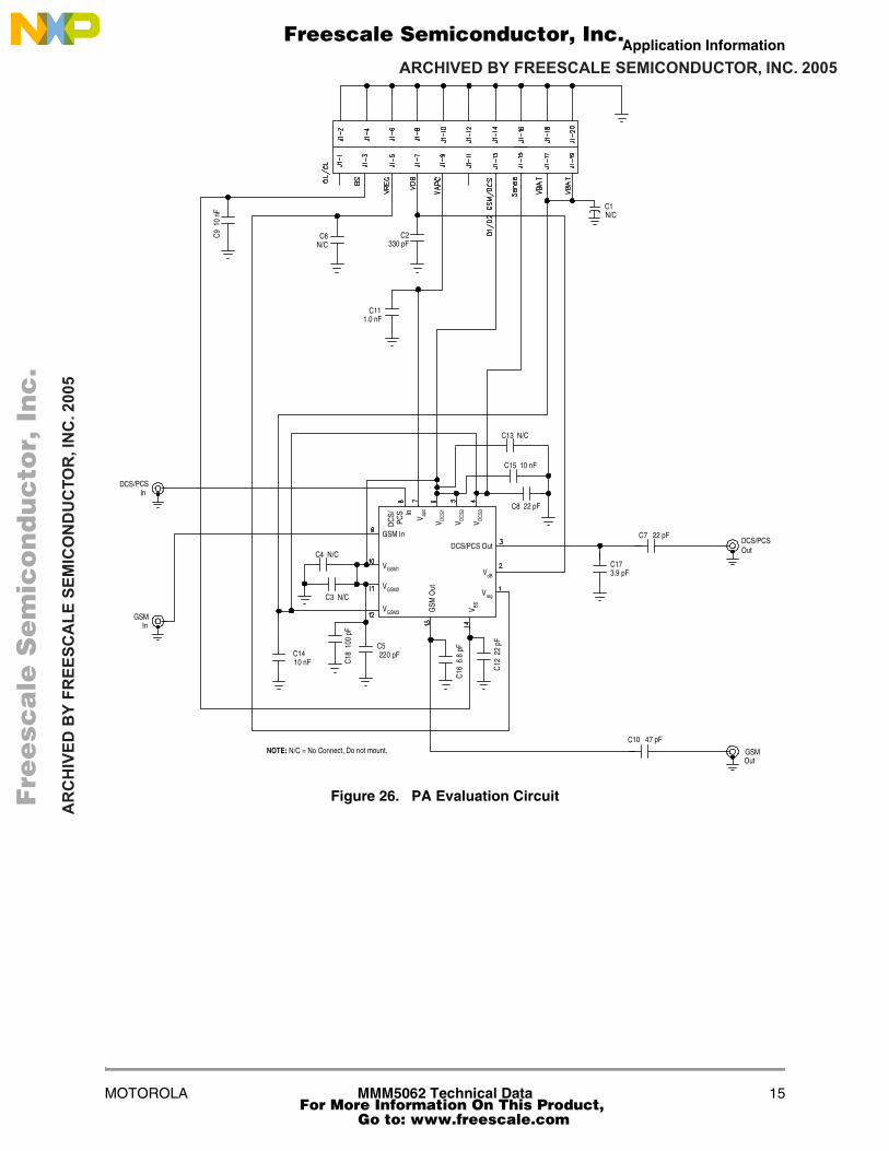
Figure 26. PA Evaluation Circuit
DCS/PCSOut
GSMOut
C7 22 pF
C10 47 pF
C173.9 pF
C12
22
pF
C16
6.8
pFC5
220 pF
C18
100
pF
C1410 nF
C3 N/C
C4 N/C
C8 22 pF
C15 10 nF
C13 N/C
GSM In
VGSM1
VGSM2
VGSM3
DCS/PCS Out
VdB
Vreg
V BSGSM
Out
V DC
S3
V DC
S 2
V DC
S1
V apc
DC
S/PC
S In
C111.0 nF
C2330 pF
C6N/C
C9
10
nFC1N/C
NOTE: N/C = No Connect, Do not mount.
GSMIn
DCS/PCSIn
Fre
esc
ale
Se
mic
on
du
cto
r, I
Freescale Semiconductor, Inc.
For More Information On This Product, Go to: www.freescale.com
nc
...
ARCHIVED BY FREESCALE SEMICONDUCTOR, INC. 2005A
RC
HIV
ED
BY
FR
EE
SC
AL
E S
EM
ICO
ND
UC
TOR
, IN
C. 2
005
16 MMM5062 Technical Data MOTOROLA
Application Information
Figure 27. Power Amplifier Control Loop
C168 µF
R3 12 k
C3 15 pF
C4330 pF
R6 39 k
R45.6 k
R55.6 k
R11 150 Ω
C1810 nF
R2 150 Ω
C5 10 nFC647 nF
R8 1.0 k
R7 560 Ω
R10 N/C
C2 330 pF
C12 10 nF
NOTE: N/C = No Connect, Do not mount.
Fre
esc
ale
Se
mic
on
du
cto
r, I
Freescale Semiconductor, Inc.
For More Information On This Product, Go to: www.freescale.com
nc
...
ARCHIVED BY FREESCALE SEMICONDUCTOR, INC. 2005A
RC
HIV
ED
BY
FR
EE
SC
AL
E S
EM
ICO
ND
UC
TOR
, IN
C. 2
005
Application Information
MOTOROLA MMM5062 Technical Data 17
Figure 28. PA Evaluation Circuit PCB
Table 6. PA Evaluation Circuit PCB Bill of Materials
Reference Value Part Number Manufacturer
C1, C3, C4, C6, C13 N/C - Do not mount
C2 330 pF GRM36COG330J50 Murata
C5 220 pF GRM36X7R221K50 Murata
C7, C8, C12 22 pF GRM36COG220J50 Murata
C9, C14, C15 10 nF GRM36X7R103K25 Murata
C10 47 pF GRM36COG470J50 Murata
C11 1.0 nF GRM36X7R102K25 Murata
C16 6.8 pF GRM36COG6R8J50 Murata
C17 3.9 pF GRM36COG3R9J50 Murata
C18 100 nF GRM36X7R104K25 Murata
J2, J3, J4, J5 50 Ω 142-0711-821 Johnson
Fre
esc
ale
Se
mic
on
du
cto
r, I
Freescale Semiconductor, Inc.
For More Information On This Product, Go to: www.freescale.com
nc
...
ARCHIVED BY FREESCALE SEMICONDUCTOR, INC. 2005A
RC
HIV
ED
BY
FR
EE
SC
AL
E S
EM
ICO
ND
UC
TOR
, IN
C. 2
005
18 MMM5062 Technical Data MOTOROLA
Application Information
Figure 29. Power Amplifier Control Loop PCB
Table 7. Power Amplifier Control Loop PCB Bill of Materials
Reference Value Part Number Manufacturer
C1 68 µF 293D685X9020C Sprague
C2 330 pF GRM36COG330J50 Murata
C3 15 pF GRM36COG150J50 Murata
C4 330 pF GRM36x7R331K50 Murata
C5, C12, C18 10 nF GRM36X7R103K25 Murata
C6 47 nF GRM36X7R473K10 Murata
J1, J2, J3 DC connector
Q1 Power MOSFET NTHS5445T ON Semiconductor
Q2 N/C - Do not mount
R1, R8 1.0 k CRG0402 5% 1 kO NEOHM
R2 150 Ω CRG0402 5% 150 O NEOHM
R3 12 k CRG0402 5% 12 kO NEOHM
R4, R5 5.6 k CRG0402 5% 5.6 kO NEOHM
R6, R10 N/C - Do not mount
R7 560 Ω CRG0402 5% 560 O NEOHM
R11 100 Ω CRG0402 5% 100 O NEOHM
U1 CMOS Op Amp AD8591 Analog Devices
Fre
esc
ale
Se
mic
on
du
cto
r, I
Freescale Semiconductor, Inc.
For More Information On This Product, Go to: www.freescale.com
nc
...
ARCHIVED BY FREESCALE SEMICONDUCTOR, INC. 2005A
RC
HIV
ED
BY
FR
EE
SC
AL
E S
EM
ICO
ND
UC
TOR
, IN
C. 2
005
Packaging Information
MOTOROLA MMM5062 Technical Data 19
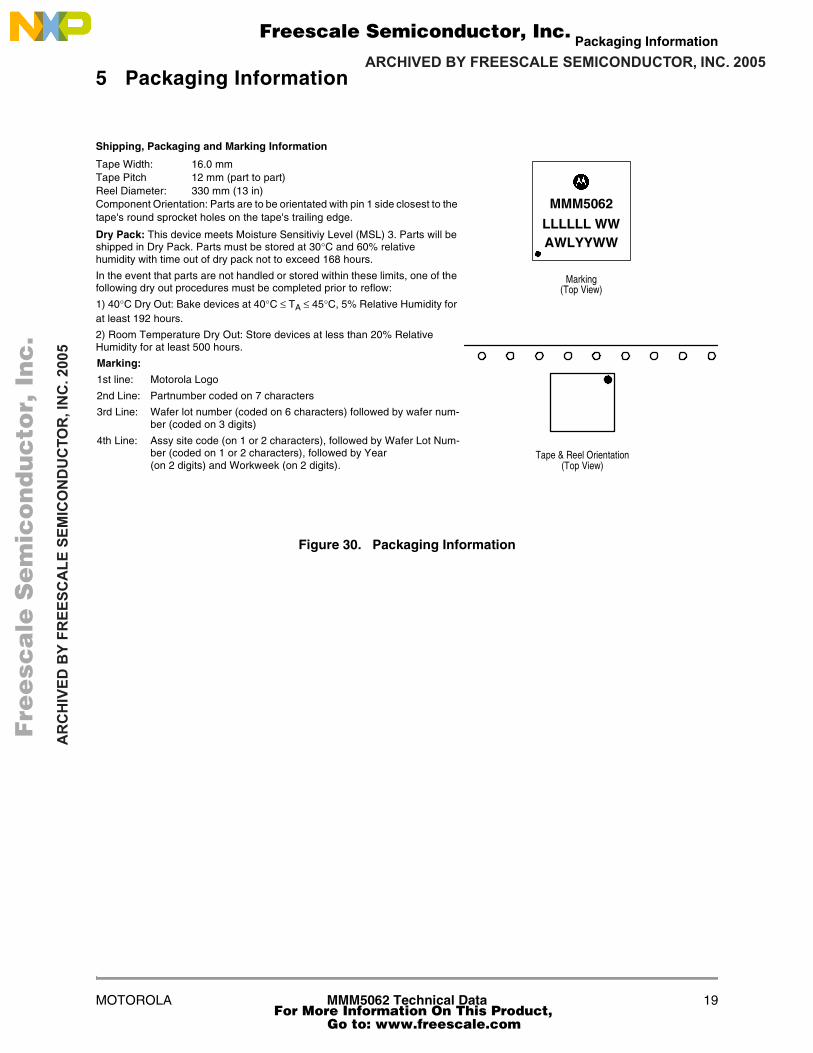
5 Packaging Information
Figure 30. Packaging Information
Marking(Top View)
MMM5062
AWLYYWWLLLLLL WW
Tape & Reel Orientation(Top View)
Tape Width: 16.0 mmTape Pitch 12 mm (part to part)Reel Diameter: 330 mm (13 in)Component Orientation: Parts are to be orientated with pin 1 side closest to the tape's round sprocket holes on the tape's trailing edge.
Dry Pack: This device meets Moisture Sensitiviy Level (MSL) 3. Parts will be shipped in Dry Pack. Parts must be stored at 30°C and 60% relative humidity with time out of dry pack not to exceed 168 hours.
In the event that parts are not handled or stored within these limits, one of the following dry out procedures must be completed prior to reflow:
1) 40°C Dry Out: Bake devices at 40°C ≤ TA ≤ 45°C, 5% Relative Humidity for at least 192 hours.
2) Room Temperature Dry Out: Store devices at less than 20% Relative Humidity for at least 500 hours.
Marking:
1st line: Motorola Logo
2nd Line: Partnumber coded on 7 characters
3rd Line: Wafer lot number (coded on 6 characters) followed by wafer num-ber (coded on 3 digits)
4th Line: Assy site code (on 1 or 2 characters), followed by Wafer Lot Num-ber (coded on 1 or 2 characters), followed by Year (on 2 digits) and Workweek (on 2 digits).
Shipping, Packaging and Marking Information
Fre
esc
ale
Se
mic
on
du
cto
r, I
Freescale Semiconductor, Inc.
For More Information On This Product, Go to: www.freescale.com
nc
...
ARCHIVED BY FREESCALE SEMICONDUCTOR, INC. 2005A
RC
HIV
ED
BY
FR
EE
SC
AL
E S
EM
ICO
ND
UC
TOR
, IN
C. 2
005
20 MMM5062 Technical Data MOTOROLA
Packaging Information
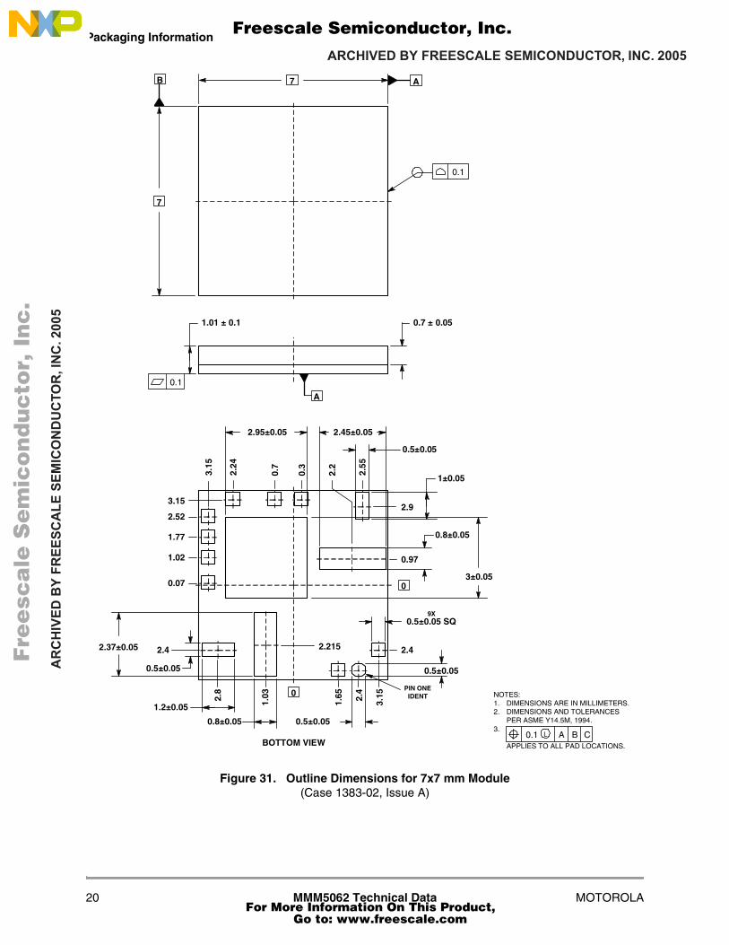
Figure 31. Outline Dimensions for 7x7 mm Module(Case 1383-02, Issue A)
7
B
0.1
A7
A
0.1
1.01 ± 0.1 0.7 ± 0.05
0
0.5±0.05
03±0.05
BOTTOM VIEW
2.37±0.05
0.5±0.05
0.5±0.050.8±0.05
1.2±0.05
2.9
0.97
2.4
3.152.4
1.65
1.032.8
2.4
2.55
0.07
1.02
1.77
2.52
3.15
2.2
0.3
0.7
2.24
3.15
2.215
0.5±0.05 SQ
0.8±0.05
9X
PIN ONEIDENT
1±0.05
0.5±0.05
2.45±0.052.95±0.05
NOTES:1. DIMENSIONS ARE IN MILLIMETERS.2. DIMENSIONS AND TOLERANCES
PER ASME Y14.5M, 1994.3.
APPLIES TO ALL PAD LOCATIONS.
L B0.1 CA
Fre
esc
ale
Se
mic
on
du
cto
r, I
Freescale Semiconductor, Inc.
For More Information On This Product, Go to: www.freescale.com
nc
...
ARCHIVED BY FREESCALE SEMICONDUCTOR, INC. 2005A
RC
HIV
ED
BY
FR
EE
SC
AL
E S
EM
ICO
ND
UC
TOR
, IN
C. 2
005
MOTOROLA MMM5062 Technical Data 21
NOTES
Fre
esc
ale
Se
mic
on
du
cto
r, I
Freescale Semiconductor, Inc.
For More Information On This Product, Go to: www.freescale.com
nc
...
ARCHIVED BY FREESCALE SEMICONDUCTOR, INC. 2005A
RC
HIV
ED
BY
FR
EE
SC
AL
E S
EM
ICO
ND
UC
TOR
, IN
C. 2
005
MMM5062/D
HOW TO REACH US:
USA/EUROPE/LOCATIONS NOT LISTED:
Motorola Literature Distribution; P.O. Box 5405, Denver, Colorado 80217 1-303-675-2140 or 1-800-441-2447
JAPAN:
Motorola Japan Ltd.; SPS, Technical Information Center, 3-20-1, Minami-Azabu Minato-ku, Tokyo 106-8573 Japan81-3-3440-3569
ASIA/PACIFIC:
Motorola Semiconductors H.K. Ltd.; Silicon Harbour Centre, 2 Dai King Street, Tai Po Industrial Estate, Tai Po, N.T., Hong Kong852-26668334
TECHNICAL INFORMATION CENTER:
1-800-521-6274
HOME PAGE:
http://www.motorola.com/semiconductors
Information in this document is provided solely to enable system and software implementers to
use Motorola products. There are no express or implied copyright licenses granted hereunder to
design or fabricate any integrated circuits or integrated circuits based on the information in this
document.
Motorola reserves the right to make changes without further notice to any products herein.
Motorola makes no warranty, representation or guarantee regarding the suitability of its products
for any particular purpose, nor does Motorola assume any liability arising out of the application or
use of any product or circuit, and specifically disclaims any and all liability, including without
limitation consequential or incidental damages. “Typical” parameters which may be provided in
Motorola data sheets and/or specifications can and do vary in different applications and actual
performance may vary over time. All operating parameters, including “Typicals” must be validated
for each customer application by customer’s technical experts. Motorola does not convey any
license under its patent rights nor the rights of others. Motorola products are not designed,
intended, or authorized for use as components in systems intended for surgical implant into the
body, or other applications intended to support or sustain life, or for any other application in which
the failure of the Motorola product could create a situation where personal injury or death may
occur. Should Buyer purchase or use Motorola products for any such unintended or unauthorized
application, Buyer shall indemnify and hold Motorola and its officers, employees, subsidiaries,
affiliates, and distributors harmless against all claims, costs, damages, and expenses, and
reasonable attorney fees arising out of, directly or indirectly, any claim of personal injury or death
associated with such unintended or unauthorized use, even if such claim alleges that Motorola
was negligent regarding the design or manufacture of the part.
Motorola and the Stylized M Logo are registered in the U.S. Patent and Trademark Office. All other product or service names are the property of their respective owners. Motorola, Inc. is an Equal Opportunity/Affirmative Action Employer.
© Motorola, Inc. 2003
Fre
esc
ale
Se
mic
on
du
cto
r, I
Freescale Semiconductor, Inc.
For More Information On This Product, Go to: www.freescale.com
nc
...