
Measuring ultra-shallow junction Jialin Zhao. Resistivity and Sheet resistance IRS roadmap 2003: 10...
25
Measuring ultra-shallow junction Jialin Zhao
-
date post
19-Dec-2015 -
Category
Documents
-
view
222 -
download
0
Transcript of Measuring ultra-shallow junction Jialin Zhao. Resistivity and Sheet resistance IRS roadmap 2003: 10...
Measuring ultra-shallow junction
Jialin Zhao

Resistivity and Sheet resistance
• IRS roadmap 2003: 10 nm junction with sheet resistance 500 Ω/sq
• Electrical resistivity
• Sheet resistance
when L= W
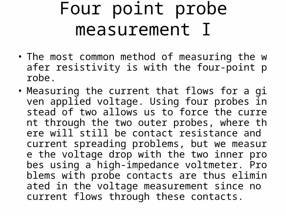
Four point probe measurement I
• The most common method of measuring the wafer resistivity is with the four-point probe.
• Measuring the current that flows for a given applied voltage. Using four probes instead of two allows us to force the current through the two outer probes, where there will still be contact resistance and current spreading problems, but we measure the voltage drop with the two inner probes using a high-impedance voltmeter. Problems with probe contacts are thus eliminated in the voltage measurement since no current flows through these contacts.
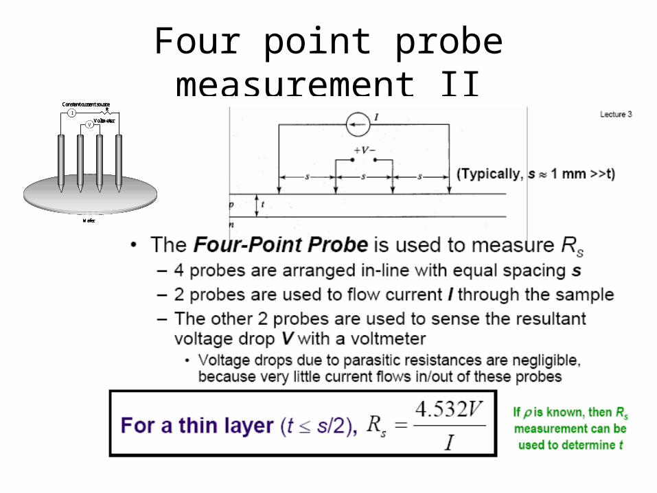
Four point probe measurement II
Wafer
R
Voltmeter
Constant current source
V
I
Wafer
R
Voltmeter
Constant current source
Wafer
R
Voltmeter
Constant current source
Wafer
R
Voltmeter
Constant current source
V
I
V
I
VV
I

Hall Effect Measurements•The Hall effect was discovered more than 100 years ago when Hall observed a transverse voltage across a conductor subjected to a magnetic field.
•The technique is more powerful than the sheet resistance method described above because it can determine the material type, carrier concentration and carrier mobility separately. The basic method is illustrated in the next slide. The left part of the figure defines the reference directions and the various currents, fields and voltages; the right part of the figure illustrates a top view of a practical geometry that is often used in semiconductor applications.
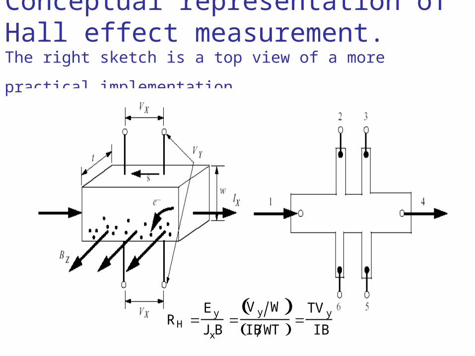
Conceptual representation of Hall effect measurement. The right sketch is a top view of a more practical implementation.
RH Ey
JxB
V y W IB WT
TVy
IB
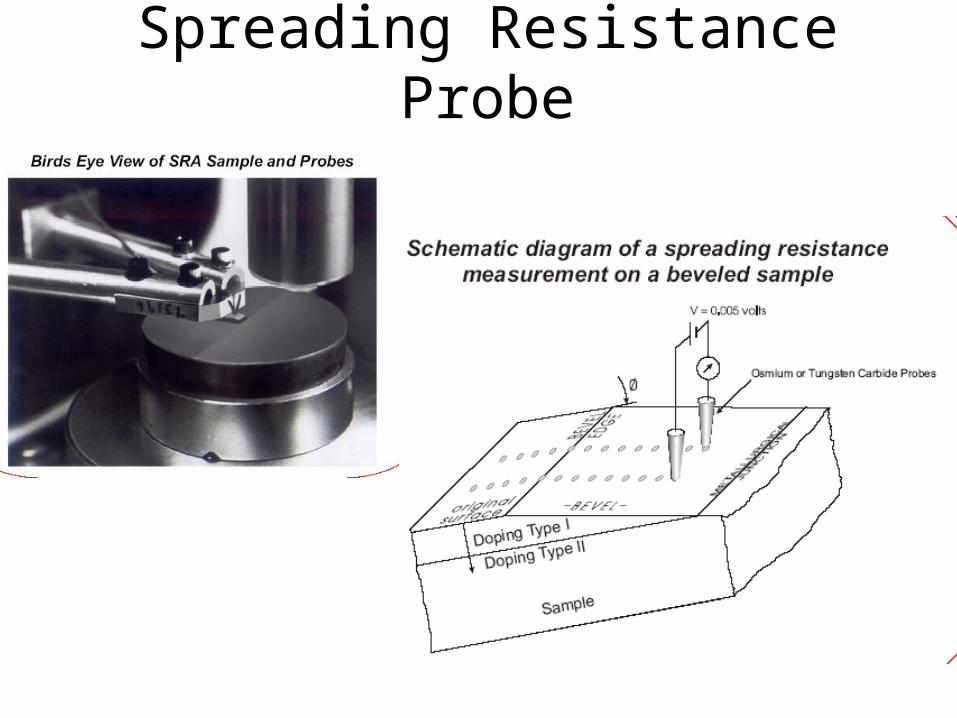
Spreading Resistance Probe
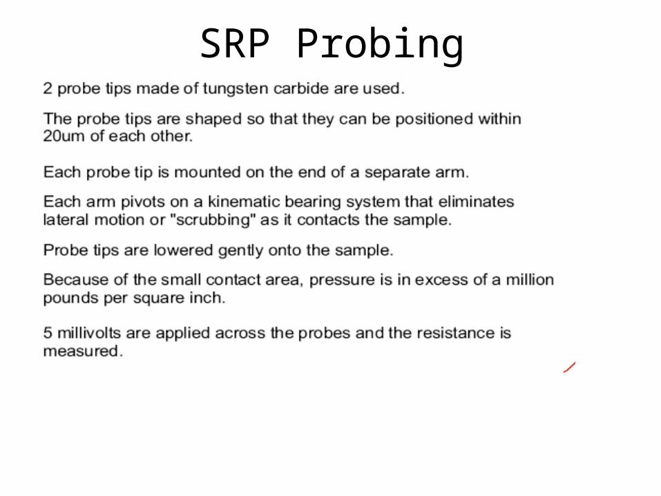
SRP Probing
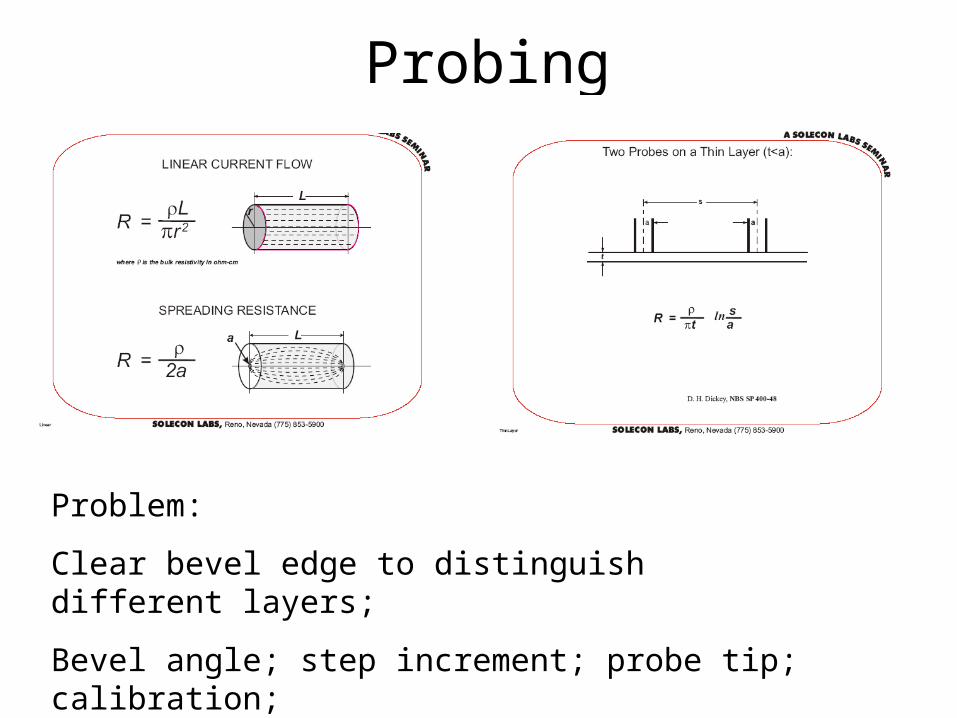
Probing
Problem:
Clear bevel edge to distinguish different layers;
Bevel angle; step increment; probe tip; calibration;
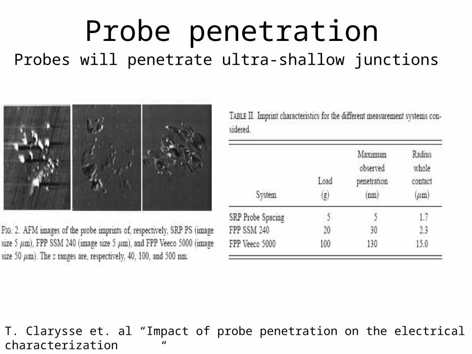
Probe penetration Probes will penetrate ultra-shallow junctions
T. Clarysse et. al “Impact of probe penetration on the electrical characterizationof sub-50 nm profiles”,J. Vac. Sci. Technol. B, Vol. 20, No. 1, Jan/Feb 2002
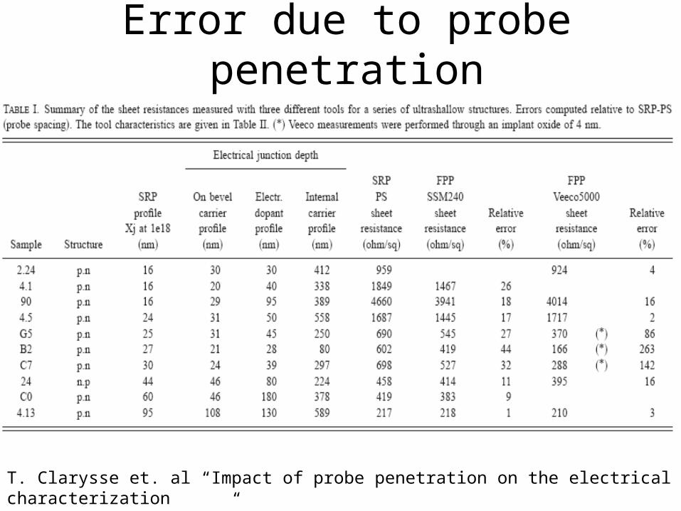
Error due to probe penetration
T. Clarysse et. al “Impact of probe penetration on the electrical characterizationof sub-50 nm profiles”,J. Vac. Sci. Technol. B, Vol. 20, No. 1, Jan/Feb 2002
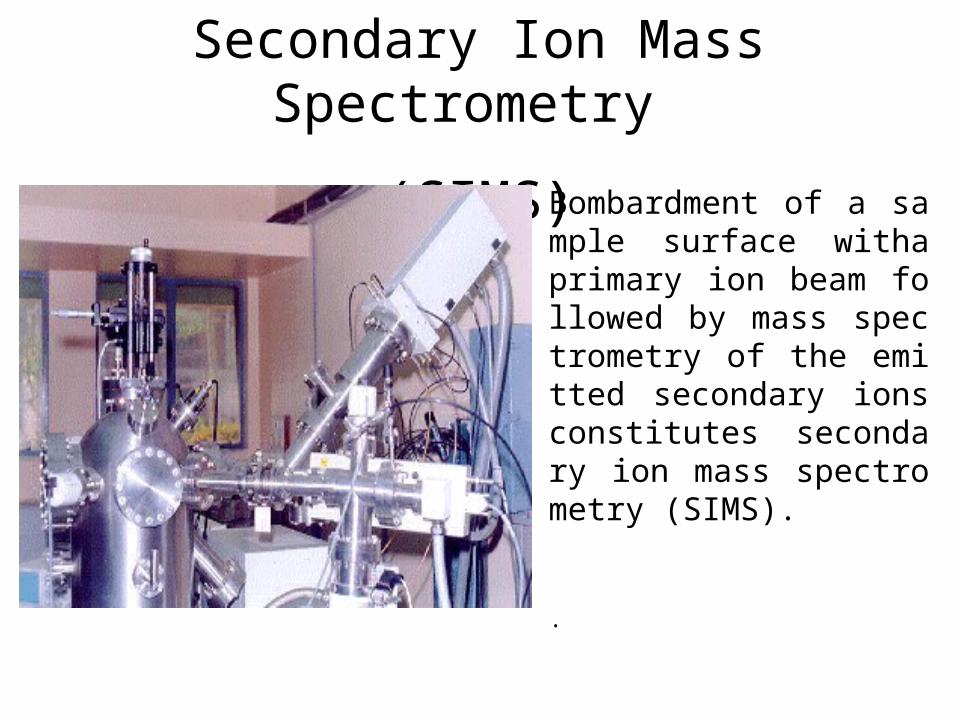
Bombardment of a sample surface witha primary ion beam followed by mass spectrometry of the emitted secondary ions constitutes secondary ion mass spectrometry (SIMS).
.
Secondary Ion Mass Spectrometry
(SIMS)
Uses
• NASA first developed SIMS in the 1960s to investigate the composition of Moon rocks.
• SIMS can be used to determine the composition of organic and inorganic solids. This can generate spatial or depth profiles of elemental or molecular concentrations.
• These profiles can be used to generate element specific images of the sample that display the varying concentrations over the area of the sample
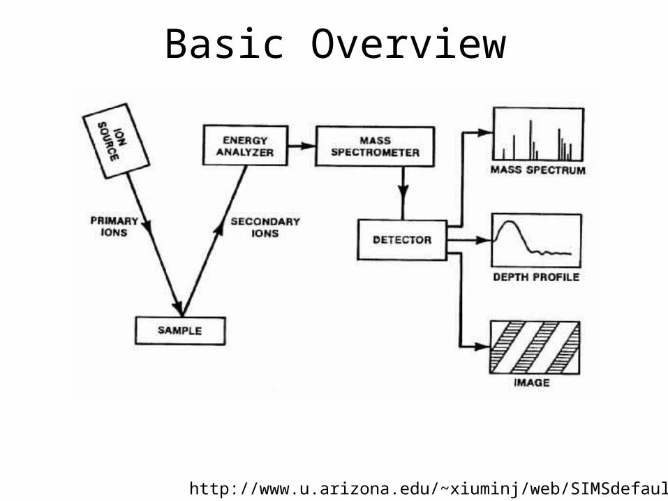
Basic Overview
http://www.u.arizona.edu/~xiuminj/web/SIMSdefault.htm
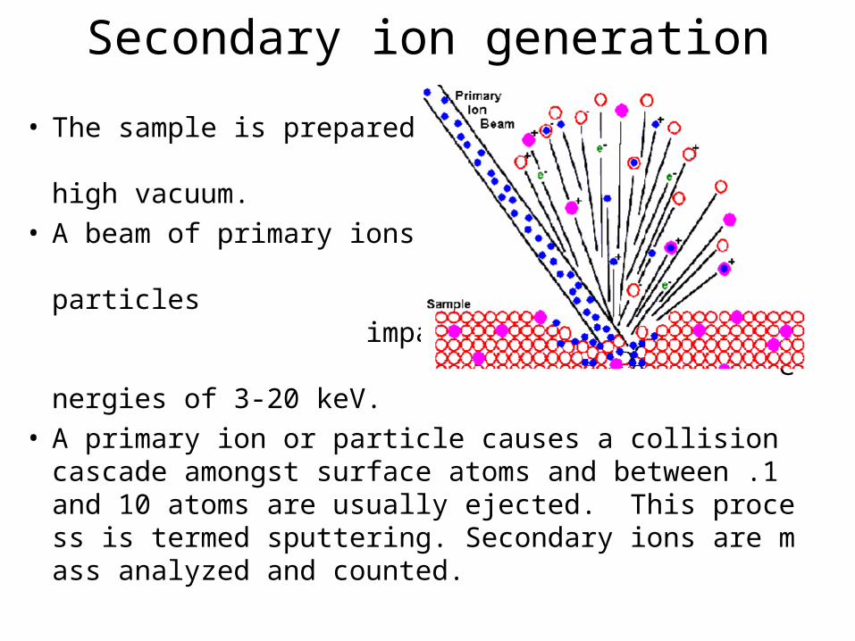
Secondary ion generation
• The sample is prepared in an ultra high vacuum.
• A beam of primary ions or neutral particles impacts the surface with energies of 3-20 keV.
• A primary ion or particle causes a collision cascade amongst surface atoms and between .1 and 10 atoms are usually ejected. This process is termed sputtering. Secondary ions are mass analyzed and counted.
Silicon doping analysis• To produce a high ion yield and a small mass interfere
nce, Cs+ is normally chosen for n-type dopants (As, P, Sb), while O2+ is chosen for p-type dopants (B, In)
• Monitoring the secondary ion count rate of selected elements as a function of time leads to depth profiles.
• To convert the time axis into depth, the SIMS analyst uses a profilometer to measure the sputter crater depth. A profilometer is a separate instrument that determines depth by dragging a stylus across the crater and noting vertical deflections. Total crater depth divided by total sputter time provides the average sputter rate
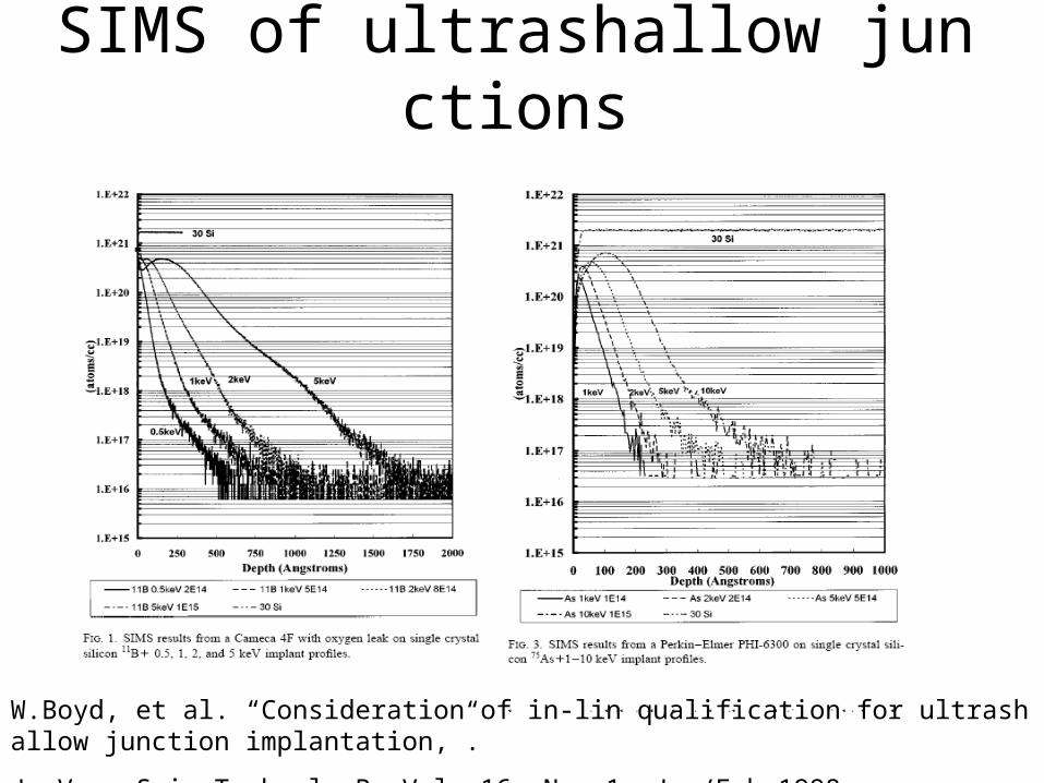
SIMS of ultrashallow junctions
W.Boyd, et al. “Consideration of in-lin qualification for ultrashallow junction implantation,”.
J. Vac. Sci. Technol. B, Vol. 16, No. 1, Jan/Feb 1998
Problems
• Chemical concentration
• Steady state in the first 5-10 nm
• Surface clean, primary ions conditions
• The limiting may be 2keV implantation
• Not an in-line process
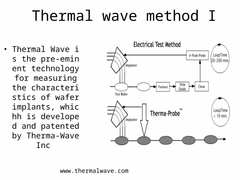
Thermal wave method I
• Thermal Wave is the pre-eminent technology for measuring the characteristics of wafer implants, whichh is developed and patented by Therma-Wave I
nc
www.thermalwave.com
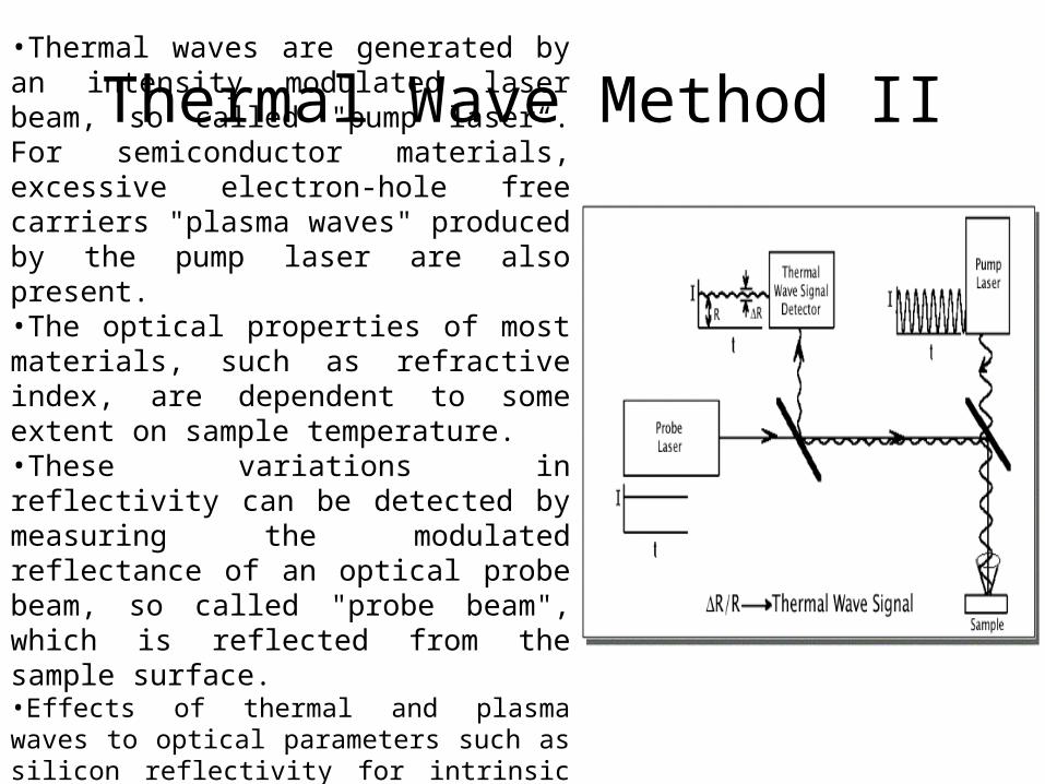
Thermal Wave Method II•Thermal waves are generated by an intensity modulated laser beam, so called "pump laser“. For semiconductor materials, excessive electron-hole free carriers "plasma waves" produced by the pump laser are also present. •The optical properties of most materials, such as refractive index, are dependent to some extent on sample temperature. •These variations in reflectivity can be detected by measuring the modulated reflectance of an optical probe beam, so called "probe beam", which is reflected from the sample surface. •Effects of thermal and plasma waves to optical parameters such as silicon reflectivity for intrinsic and heavily-doped silicon are different
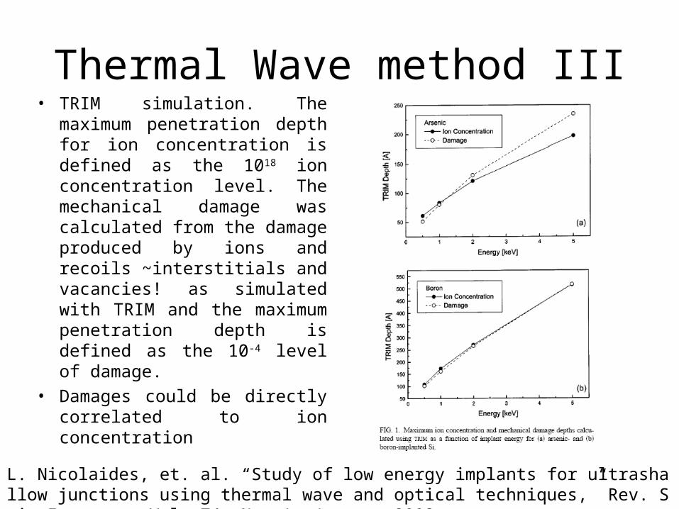
Thermal Wave method III• TRIM simulation. The
maximum penetration depth for ion concentration is defined as the 1018 ion concentration level. The mechanical damage was calculated from the damage produced by ions and recoils ~interstitials and vacancies! as simulated with TRIM and the maximum penetration depth is defined as the 10-4 level of damage.
• Damages could be directly correlated to ion concentration
L. Nicolaides, et. al. “Study of low energy implants for ultrashallow junctions using thermal wave and optical techniques,” Rev. Sci. Instrum., Vol. 74, No. 1, January 2003
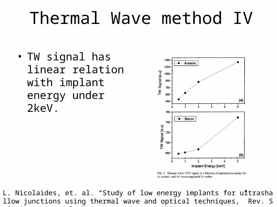
Thermal Wave method IV
• TW signal has linear relation with implant energy under 2keV.
L. Nicolaides, et. al. “Study of low energy implants for ultrashallow junctions using thermal wave and optical techniques,” Rev. Sci. Instrum., Vol. 74, No. 1, January 2003
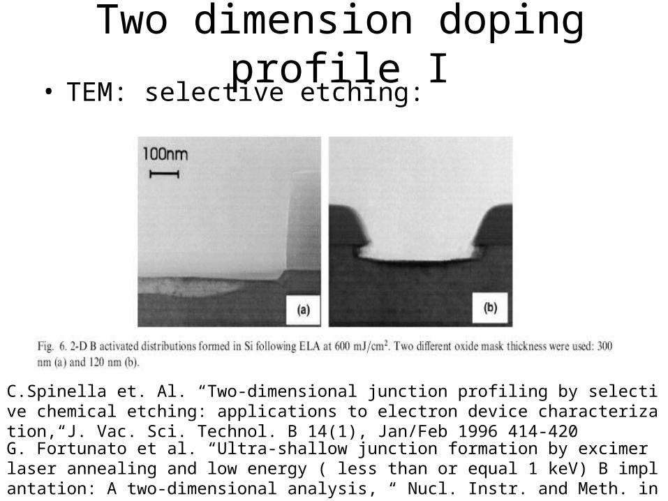
Two dimension doping profile I• TEM: selective etching: HF+HNO3+CH3COOH
G. Fortunato et al. “Ultra-shallow junction formation by excimer laser annealing and low energy ( less than or equal 1 keV) B implantation: A two-dimensional analysis, “ Nucl. Instr. and Meth. in Phys. Res. B 186 (2002) 401–408
C.Spinella et. Al. “Two-dimensional junction profiling by selective chemical etching: applications to electron device characterization,“J. Vac. Sci. Technol. B 14(1), Jan/Feb 1996 414-420
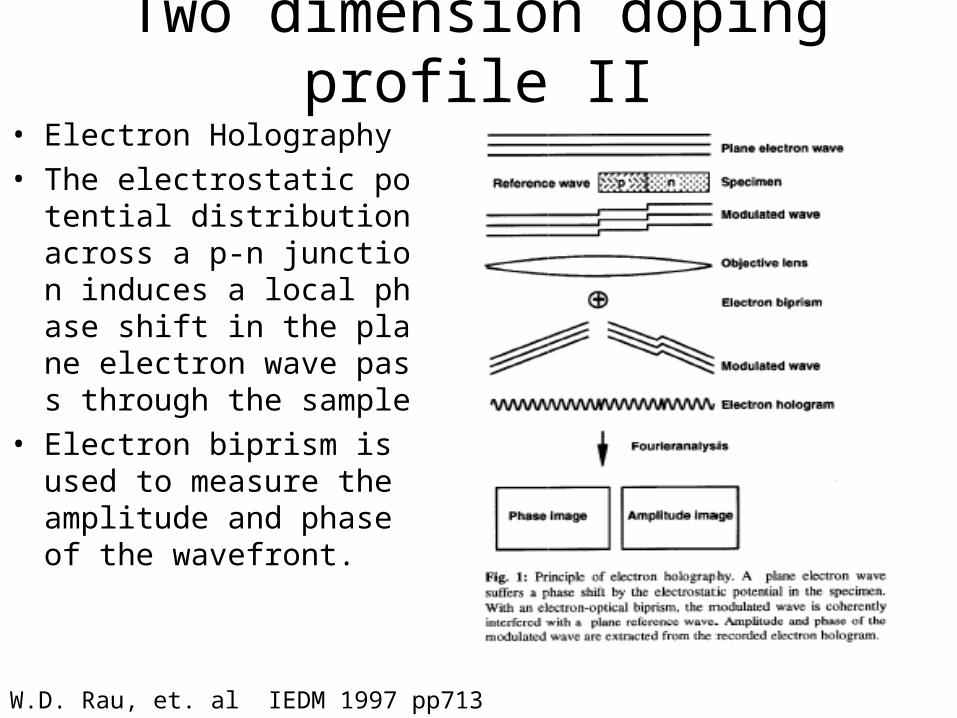
Two dimension doping profile II• Electron Holography• The electrostatic potential
distribution across a p-n junction induces a local phase shift in the plane electron wave pass through the sample
• Electron biprism is used to measure the amplitude and phase of the wavefront.
W.D. Rau, et. al IEDM 1997 pp713
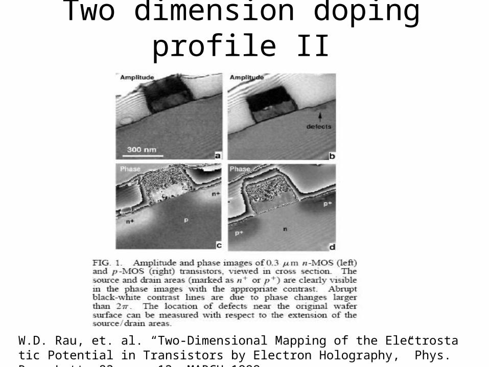
Two dimension doping profile II
W.D. Rau, et. al. “Two-Dimensional Mapping of the Electrostatic Potential in Transistors by Electron Holography,” Phys. Rev. Lett. 82 , no 12, MARCH 1999


![Gamma Radiation-Induced Disruption of Cellular Junctions ...downloads.hindawi.com/journals/omcl/2019/1486232.pdf · junction protein [13]. Connexins compose the gap junction channels](https://static.fdocument.org/doc/165x107/5f06b4cd7e708231d4195458/gamma-radiation-induced-disruption-of-cellular-junctions-junction-protein-13.jpg)


![Exam 1 Crib Sheetssawyer/CircuitsFall2019_all/... · 2019-12-16 · Exam 3 Crib Sheet Impedance, Z [Ω], properties have the same characteristics as resistance In series add, ZEQ](https://static.fdocument.org/doc/165x107/5e6864eb079aa85e6443e07b/exam-1-crib-sheet-ssawyercircuitsfall2019all-2019-12-16-exam-3-crib-sheet.jpg)