MCP6411 1MHz Operational Amplifier with EMI Filtering• Analog Active Filters ... The Microchip...
34
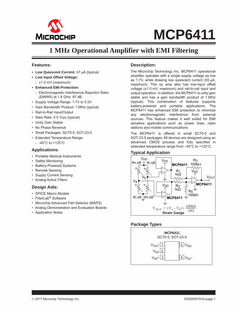
2017 Microchip Technology Inc. DS20005791A-page 1 MCP6411 Features: • Low Quiescent Current: 47 μA (typical) • Low Input Offset Voltage: - ±1.0 mV (maximum) • Enhanced EMI Protection: - Electromagnetic Interference Rejection Ratio (EMIRR) at 1.8 GHz: 97 dB • Supply Voltage Range: 1.7V to 5.5V • Gain Bandwidth Product: 1 MHz (typical) • Rail-to-Rail Input/Output • Slew Rate: 0.5 V/μs (typical) • Unity Gain Stable • No Phase Reversal • Small Packages: SC70-5, SOT-23-5 • Extended Temperature Range: - -40°C to +125°C Applications: • Portable Medical Instruments • Safety Monitoring • Battery-Powered Systems • Remote Sensing • Supply Current Sensing • Analog Active Filters Design Aids: • SPICE Macro Models • FilterLab ® Software • Microchip Advanced Part Selector (MAPS) • Analog Demonstration and Evaluation Boards • Application Notes Description: The Microchip Technology Inc. MCP6411 operational amplifier operates with a single supply voltage as low as 1.7V, while drawing low quiescent current (55 μA, maximum). This op amp also has low-input offset voltage (±1.0 mV, maximum) and rail-to-rail input and output operation. In addition, the MCP6411 is unity gain stable and has a gain bandwidth product of 1 MHz (typical). This combination of features supports battery-powered and portable applications. The MCP6411 has enhanced EMI protection to minimize any electromagnetic interference from external sources. This feature makes it well suited for EMI sensitive applications such as power lines, radio stations and mobile communications. The MCP6411 is offered in small SC70-5 and SOT-23-5 packages. All devices are designed using an advanced CMOS process and fully specified in extended temperature range from –40°C to +125°C. Typical Application Package Types V DD R 2 + - V OUT MCP64 1 R 1 R 3 100k R 5 100k 1k 1k R- R R+ R V a V b V DD + - V DD + - MCP64 1 MCP64 1 R+ R R- R V DD Strain Gauge V OUT V a V b – 100k 1k ---------------- = 5 4 1 2 3 V DD V IN – V IN + V SS V OUT MCP6411 SC70-5, SOT-23-5 1 MHz Operational Amplifier with EMI Filtering
Transcript of MCP6411 1MHz Operational Amplifier with EMI Filtering• Analog Active Filters ... The Microchip...
MCP64111 MHz Operational Amplifier with EMI Filtering
Features:• Low Quiescent Current: 47 μA (typical)• Low Input Offset Voltage:
- ±1.0 mV (maximum)• Enhanced EMI Protection:
- Electromagnetic Interference Rejection Ratio (EMIRR) at 1.8 GHz: 97 dB
• Supply Voltage Range: 1.7V to 5.5V• Gain Bandwidth Product: 1 MHz (typical)• Rail-to-Rail Input/Output• Slew Rate: 0.5 V/μs (typical)• Unity Gain Stable• No Phase Reversal• Small Packages: SC70-5, SOT-23-5• Extended Temperature Range:
- -40°C to +125°C
Applications:• Portable Medical Instruments• Safety Monitoring• Battery-Powered Systems• Remote Sensing• Supply Current Sensing• Analog Active Filters
Design Aids:• SPICE Macro Models • FilterLab® Software• Microchip Advanced Part Selector (MAPS)• Analog Demonstration and Evaluation Boards• Application Notes
Description:The Microchip Technology Inc. MCP6411 operationalamplifier operates with a single supply voltage as lowas 1.7V, while drawing low quiescent current (55 μA,maximum). This op amp also has low-input offsetvoltage (±1.0 mV, maximum) and rail-to-rail input andoutput operation. In addition, the MCP6411 is unity gainstable and has a gain bandwidth product of 1 MHz(typical). This combination of features supportsbattery-powered and portable applications. TheMCP6411 has enhanced EMI protection to minimizeany electromagnetic interference from externalsources. This feature makes it well suited for EMIsensitive applications such as power lines, radiostations and mobile communications.
The MCP6411 is offered in small SC70-5 andSOT-23-5 packages. All devices are designed using anadvanced CMOS process and fully specified inextended temperature range from –40°C to +125°C.
Typical Application
Package Types
VDD
R2+- VOUT
MCP64 1
R1
R3100k
R5100k
1k
1k
R- R
R+ R
VaVb
VDD
+-
VDD
+-
MCP64 1
MCP64 1R+ R
R- R
VDD
Strain GaugeV OUT V a V b– 100k
1k----------------=
5
4
1
2
3
VDD
VIN–VIN+
VSS
VOUT
MCP6411SC70-5, SOT-23-5
2017 Microchip Technology Inc. DS20005791A-page 1

MCP6411
NOTES:DS20005791A-page 2 2017 Microchip Technology Inc.
MCP6411
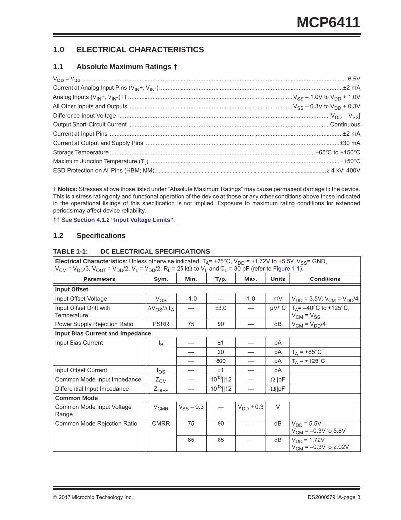
1.0 ELECTRICAL CHARACTERISTICS1.1 Absolute Maximum Ratings †VDD – VSS ..................................................................................................................................................................6.5VCurrent at Analog Input Pins (VIN+, VIN-) ................................................................................................................±2 mAAnalog Inputs (VIN+, VIN-)†† .................................................................................................... VSS – 1.0V to VDD + 1.0VAll Other Inputs and Outputs ................................................................................................... VSS – 0.3V to VDD + 0.3VDifference Input Voltage ................................................................................................................................ |VDD – VSS|Output Short-Circuit Current ..........................................................................................................................ContinuousCurrent at Input Pins ...............................................................................................................................................±2 mACurrent at Output and Supply Pins ......................................................................................................................±30 mAStorage Temperature .............................................................................................................................–65°C to +150°CMaximum Junction Temperature (TJ) ....................................................................................................................+150°CESD Protection on All Pins (HBM; MM) 4 kV; 400V
† Notice: Stresses above those listed under “Absolute Maximum Ratings” may cause permanent damage to the device.This is a stress rating only and functional operation of the device at those or any other conditions above those indicatedin the operational listings of this specification is not implied. Exposure to maximum rating conditions for extendedperiods may affect device reliability.†† See Section 4.1.2 “Input Voltage Limits”.
1.2 Specifications
TABLE 1-1: DC ELECTRICAL SPECIFICATIONS Electrical Characteristics: Unless otherwise indicated, TA= +25°C, VDD = +1.72V to +5.5V, VSS= GND, VCM = VDD/3, VOUT = VDD/2, VL = VDD/2, RL = 25 k to VL and CL = 30 pF (refer to Figure 1-1).
Parameters Sym. Min. Typ. Max. Units Conditions
Input OffsetInput Offset Voltage VOS –1.0 — 1.0 mV VDD = 3.5V; VCM = VDD/4Input Offset Drift with Temperature
VOS/TA — ±3.0 — μV/°C TA= –40°C to +125°C,VCM = VSS
Power Supply Rejection Ratio PSRR 75 90 — dB VCM = VDD/4Input Bias Current and ImpedanceInput Bias Current IB — ±1 — pA
— 20 — pA TA = +85°C— 800 — pA TA = +125°C
Input Offset Current IOS — ±1 — pACommon Mode Input Impedance ZCM — 1013||12 — ||pFDifferential Input Impedance ZDIFF — 1013||12 — |pFCommon ModeCommon Mode Input Voltage Range
VCMR VSS – 0.3 — VDD + 0.3 V
Common Mode Rejection Ratio CMRR 75 90 — dB VDD = 5.5VVCM = –0.3V to 5.8V
65 85 — dB VDD = 1.72VVCM = –0.3V to 2.02V
2017 Microchip Technology Inc. DS20005791A-page 3
MCP6411
Open-Loop GainDC Open-Loop Gain(Large Signal)
AOL 95 115 — dB 0.2 < VOUT < (VDD –0.2V)VCM= VDD/4VDD = 5.5V
OutputHigh-Level Output Voltage VOH VDD – 5.5 VDD – 2 — mV VDD = 1.72V
VDD – 7 VDD – 3 — mV VDD = 5.5VLow-Level Output Voltage VOL — VSS + 2 VSS + 5.5 mV VDD = 1.72V
— VSS + 2.5 VSS + 6.5 mV VDD = 5.5VOutput Short-Circuit Current ISC — ±6 — mA VDD = 1.72V
— ±22 — mA VDD = 5.5VPower SupplySupply Voltage VDD 1.72 — 5.5 VQuiescent Current IQ 35 47 55 μA IO = 0, VCM = VDD/4
TABLE 1-1: DC ELECTRICAL SPECIFICATIONS (CONTINUED)Electrical Characteristics: Unless otherwise indicated, TA= +25°C, VDD = +1.72V to +5.5V, VSS= GND, VCM = VDD/3, VOUT = VDD/2, VL = VDD/2, RL = 25 k to VL and CL = 30 pF (refer to Figure 1-1).
Parameters Sym. Min. Typ. Max. Units Conditions
TABLE 1-2: AC ELECTRICAL SPECIFICATIONS Electrical Characteristics: Unless otherwise indicated, TA= +25°C, VDD = +1.72V to +5.5V, VSS= GND, VCM = VDD/3, VOUT = VDD/2, VL = VDD/2, RL = 25 k to VL and CL = 30 pF (refer to Figure 1-1).
Parameters Sym. Min. Typ. Max. Units Conditions
AC ResponseGain Bandwidth Product GBWP — 1 — MHzPhase Margin PM — 68 — ° G = +1 V/VSlew Rate SR — 0.5 — V/μsNoiseInput Noise Voltage Eni — 10 — μVP-P f = 0.1 Hz to 10 HzInput Noise Voltage Density eni — 38 — nV/Hz f = 1 kHz
— 32 — nV/Hz f = 10 kHzInput Noise Current Density ini — 0.6 — fA/Hz f = 1 kHzElectromagnetic Interference Rejection Ratio
EMIRR — 79 — dB VIN = 100 mVPK, 400 MHz
— 85 — VIN = 100 mVPK,900 MHz
— 89 — VIN = 100 mVPK,1800 MHz
— 94 — VIN = 100 mVPK,2400 MHz
DS20005791A-page 4 2017 Microchip Technology Inc.
MCP6411
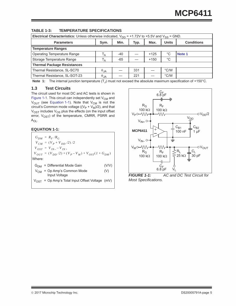
1.3 Test CircuitsThe circuit used for most DC and AC tests is shown inFigure 1-1. This circuit can independently set VCM andVOUT (see Equation 1-1). Note that VCM is not thecircuit’s Common mode voltage ((VP + VM)/2), and thatVOST includes VOS plus the effects (on the input offseterror, VOST) of the temperature, CMRR, PSRR andAOL.
EQUATION 1-1:
FIGURE 1-1: AC and DC Test Circuit for Most Specifications.
TABLE 1-3: TEMPERATURE SPECIFICATIONS Electrical Characteristics: Unless otherwise indicated, VDD = +1.72V to +5.5V and VSS = GND.
Parameters Sym. Min. Typ. Max. Units Conditions
Temperature RangesOperating Temperature Range TA -40 — +125 °C Note 1Storage Temperature Range TA -65 — +150 °CThermal Package ResistancesThermal Resistance, 5L-SC70 JA — 331 — °C/WThermal Resistance, 5L-SOT-23 JA — 221 — °C/WNote 1: The internal junction temperature (TJ) must not exceed the absolute maximum specification of +150°C.
GDM RF RG=
V CM V P V DD 2+ 2=
V OUT V DD 2 V P V M– V OST 1 GDM+ + +=
Where:
GDM = Differential Mode Gain (V/V)VCM = Op Amp’s Common Mode
Input Voltage(V)
VOST = Op Amp’s Total Input Offset Voltage (mV)
V OST V IN – V IN +–=
VDD
RG RF
VOUTVM
CB2
CLRL
VL
CB1
100 k100 k
RG RF
VDD/2VP
100 k100 k
30 pF25 k
1 μF100 nF
VIN–
VIN+
CF6.8 pF
CF6.8 pF
MCP6411
2017 Microchip Technology Inc. DS20005791A-page 5
MCP6411
NOTES:DS20005791A-page 6 2017 Microchip Technology Inc.
MCP6411
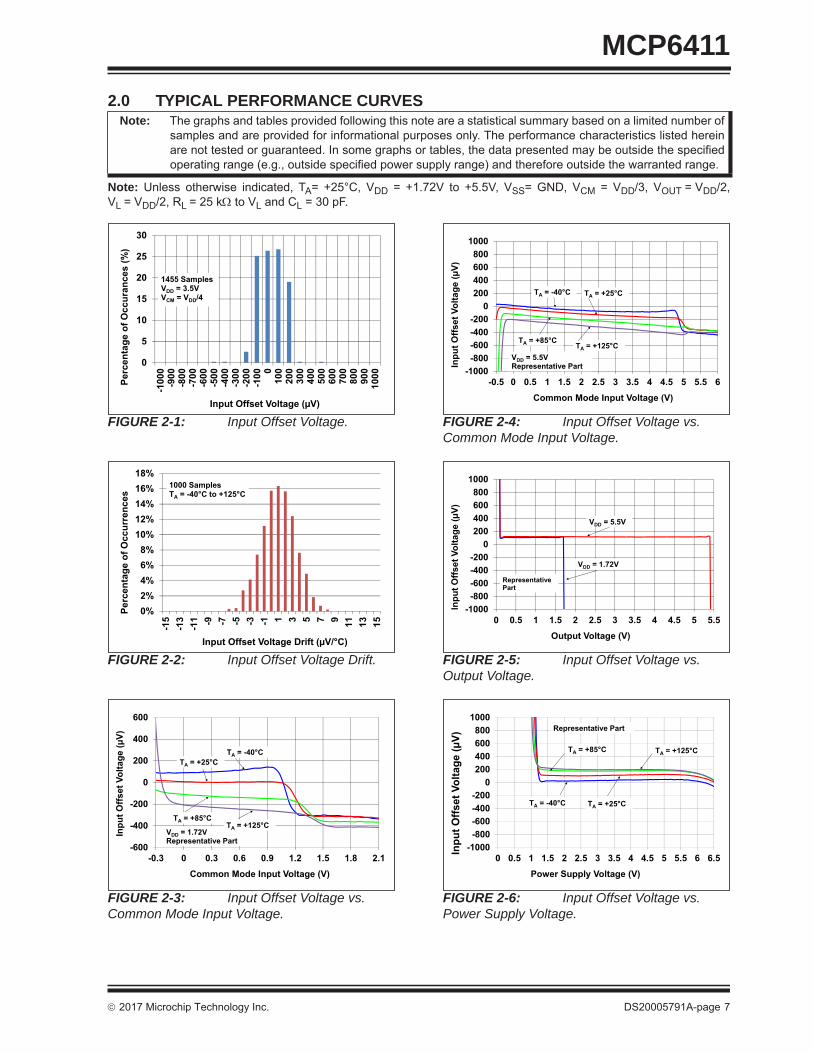
2.0 TYPICAL PERFORMANCE CURVESNote: Unless otherwise indicated, TA= +25°C, VDD = +1.72V to +5.5V, VSS= GND, VCM = VDD/3, VOUT = VDD/2,VL = VDD/2, RL = 25 k to VL and CL = 30 pF.
FIGURE 2-1: Input Offset Voltage.
FIGURE 2-2: Input Offset Voltage Drift.
FIGURE 2-3: Input Offset Voltage vs. Common Mode Input Voltage.
FIGURE 2-4: Input Offset Voltage vs. Common Mode Input Voltage.
FIGURE 2-5: Input Offset Voltage vs. Output Voltage.
FIGURE 2-6: Input Offset Voltage vs. Power Supply Voltage.
Note: The graphs and tables provided following this note are a statistical summary based on a limited number ofsamples and are provided for informational purposes only. The performance characteristics listed hereinare not tested or guaranteed. In some graphs or tables, the data presented may be outside the specifiedoperating range (e.g., outside specified power supply range) and therefore outside the warranted range.
0
5
10
15
20
25
30
-100
0-9
00-8
00-7
00-6
00-5
00-4
00-3
00-2
00-1
00 010
020
030
040
050
060
070
080
090
010
00Perc
enta
ge o
f Occ
uran
ces
(%)
Input Offset Voltage (μV)
1455 SamplesVDD = 3.5VVCM = VDD/4
0%2%4%6%8%
10%12%14%16%18%
-15
-13
-11 -9 -7 -5 -3 -1 1 3 5 7 9 11 13 15
Perc
enta
ge o
f Occ
urre
nces
Input Offset Voltage Drift (μV/°C)
1000 SamplesTA = -40°C to +125°C
-600
-400
-200
0
200
400
600
-0.3 0 0.3 0.6 0.9 1.2 1.5 1.8 2.1
Inpu
t Offs
et V
olta
ge (μ
V)
Common Mode Input Voltage (V)
VDD = 1.72VRepresentative Part
TA = +125°CTA = +85°C
TA = +25°CTA = -40°C
-1000-800-600-400-200
0200400600800
1000
-0.5 0 0.5 1 1.5 2 2.5 3 3.5 4 4.5 5 5.5 6
Inpu
t Offs
et V
olta
ge (μ
V)
Common Mode Input Voltage (V)
VDD = 5.5VRepresentative Part
TA = +125°CTA = +85°C
TA = +25°CTA = -40°C
-1000-800-600-400-200
0200400600800
1000
0 0.5 1 1.5 2 2.5 3 3.5 4 4.5 5 5.5
Inpu
t Offs
et V
olta
ge (μ
V)
Output Voltage (V)
Representative Part
VDD = 5.5V
VDD = 1.72V
-1000-800-600-400-200
0200400600800
1000
0 0.5 1 1.5 2 2.5 3 3.5 4 4.5 5 5.5 6 6.5Inpu
t Offs
et V
olta
ge (μ
V)
Power Supply Voltage (V)
Representative Part
TA = -40°C TA = +25°C
TA = +85°C TA = +125°C
2017 Microchip Technology Inc. DS20005791A-page 7
MCP6411
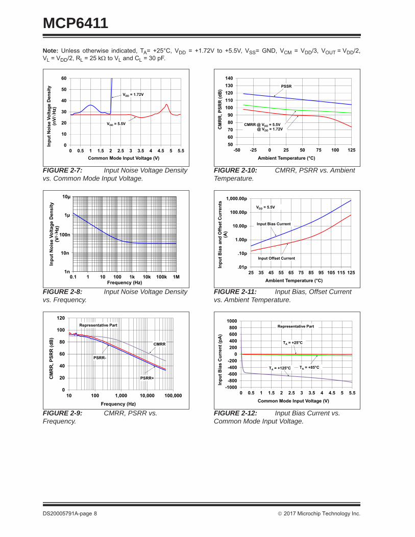
Note: Unless otherwise indicated, TA= +25°C, VDD = +1.72V to +5.5V, VSS= GND, VCM = VDD/3, VOUT = VDD/2,VL = VDD/2, RL = 25 k to VL and CL = 30 pF.FIGURE 2-7: Input Noise Voltage Density vs. Common Mode Input Voltage.
FIGURE 2-8: Input Noise Voltage Density vs. Frequency.
FIGURE 2-9: CMRR, PSRR vs. Frequency.
FIGURE 2-10: CMRR, PSRR vs. Ambient Temperature.
FIGURE 2-11: Input Bias, Offset Current vs. Ambient Temperature.
FIGURE 2-12: Input Bias Current vs. Common Mode Input Voltage.
0
10
20
30
40
50
60
0 0.5 1 1.5 2 2.5 3 3.5 4 4.5 5 5.5
Inpu
t Noi
se V
olta
ge D
ensi
ty
(nV/
Hz)
Common Mode Input Voltage (V)
VDD = 1.72V
VDD = 5.5V
1
10
100
1000
10000
1.E-1 1.E+0 1.E+1 1.E+2 1.E+3 1.E+4 1.E+5 1.E+6
Inpu
t Noi
se V
olta
ge D
ensi
ty(V
/H
z)
Frequency (Hz)0.1 1 10 100 1k 10k 100k 1M
10n
100n
1μ
1n
10μ
0
20
40
60
80
100
120
10 100 1,000 10,000 100,000
CM
RR
, PSR
R (d
B)
Frequency (Hz)
CMRR
PSRR-
PSRR+
Representative Part
5060708090
100110120130140
-50 -25 0 25 50 75 100 125
CM
RR
, PSR
R (d
B)
Ambient Temperature (°C)
PSSR
CMRR @ VDD = 5.5V@ VDD = 1.72V
.01p
.10p
1.00p
10.00p
100.00p
1,000.00p
25 35 45 55 65 75 85 95 105 115 125
Inpu
t Bia
s an
d O
ffset
Cur
rent
s (A
)
Ambient Temperature (°C)
Input Offset Current
Input Bias Current
VDD = 5.5V
-1000-800-600-400-200
0200400600800
1000
0 0.5 1 1.5 2 2.5 3 3.5 4 4.5 5 5.5
Inpu
t Bia
s C
urre
nt (p
A)
Common Mode Input Voltage (V)
Representative Part
TA = +125°C TA = +85°C
TA = +25°C
DS20005791A-page 8 2017 Microchip Technology Inc.
MCP6411
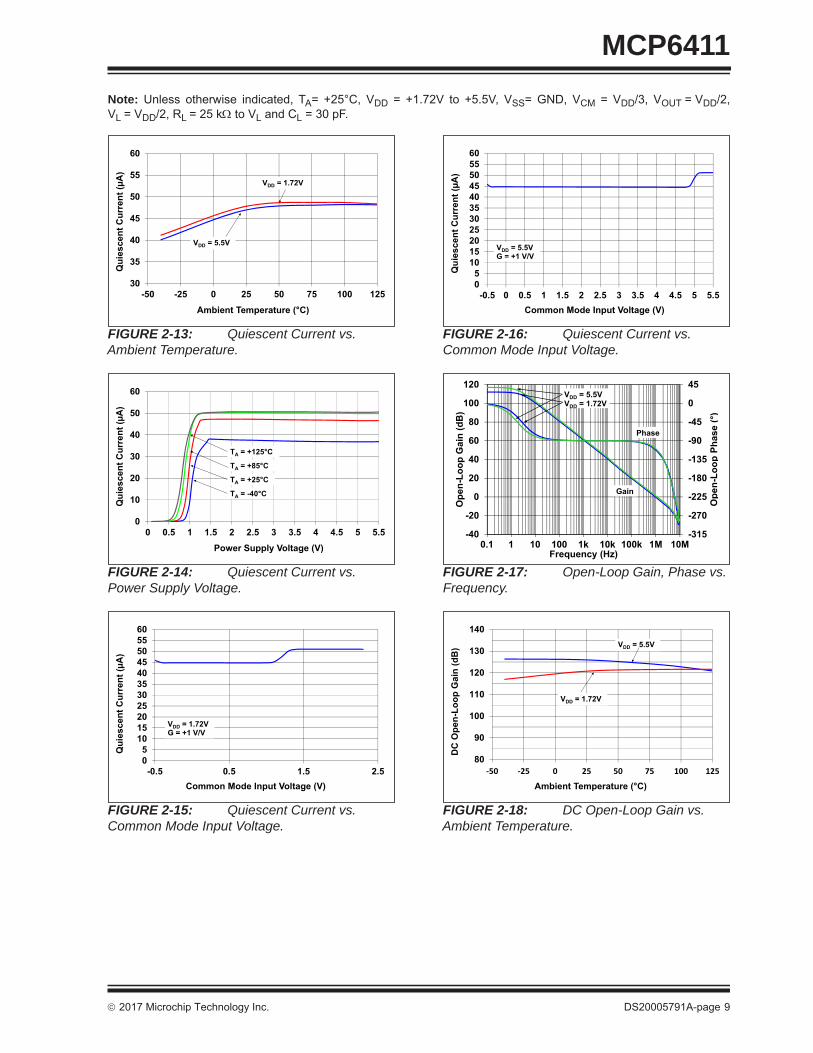
Note: Unless otherwise indicated, TA= +25°C, VDD = +1.72V to +5.5V, VSS= GND, VCM = VDD/3, VOUT = VDD/2,VL = VDD/2, RL = 25 k to VL and CL = 30 pF.FIGURE 2-13: Quiescent Current vs. Ambient Temperature.
FIGURE 2-14: Quiescent Current vs. Power Supply Voltage.
FIGURE 2-15: Quiescent Current vs. Common Mode Input Voltage.
FIGURE 2-16: Quiescent Current vs. Common Mode Input Voltage.
FIGURE 2-17: Open-Loop Gain, Phase vs. Frequency.
FIGURE 2-18: DC Open-Loop Gain vs. Ambient Temperature.
30
35
40
45
50
55
60
-50 -25 0 25 50 75 100 125
Qui
esce
nt C
urre
nt (μ
A)
Ambient Temperature (°C)
VDD = 5.5V
VDD = 1.72V
0
10
20
30
40
50
60
0 0.5 1 1.5 2 2.5 3 3.5 4 4.5 5 5.5
Qui
esce
nt C
urre
nt (μ
A)
Power Supply Voltage (V)
TA = +125°C
TA = -40°C
TA = +25°C
TA = +85°C
05
1015202530354045505560
-0.5 0.5 1.5 2.5
Qui
esce
nt C
urre
nt (μ
A)
Common Mode Input Voltage (V)
VDD = 1.72VG = +1 V/V
05
1015202530354045505560
-0.5 0 0.5 1 1.5 2 2.5 3 3.5 4 4.5 5 5.5
Qui
esce
nt C
urre
nt (μ
A)
Common Mode Input Voltage (V)
VDD = 5.5VG = +1 V/V
-315
-270
-225
-180
-135
-90
-45
0
45
-40
-20
0
20
40
60
80
100
120
1.E-11.E+01.E+11.E+21.E+31.E+41.E+51.E+61.E+7
Ope
n-Lo
op P
hase
(°)
Ope
n-Lo
op G
ain
(dB
)
Frequency (Hz)0.1 1 10 100 1k 10k 100k 1M 10M
Phase
Gain
VDD = 5.5VVDD = 1.72V
80
90
100
110
120
130
140
-50 -25 0 25 50 75 100 125
DC
Ope
n-Lo
op G
ain
(dB
)
Ambient Temperature (°C)
VDD = 5.5V
VDD = 1.72V
2017 Microchip Technology Inc. DS20005791A-page 9
MCP6411
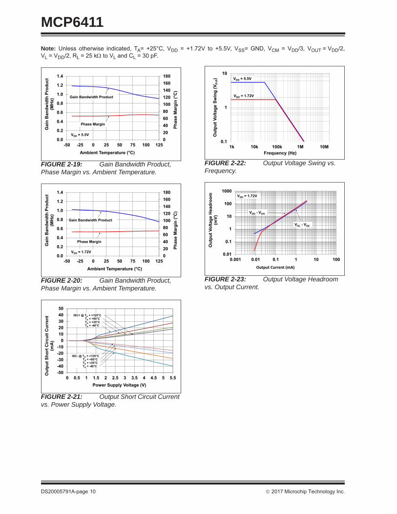
Note: Unless otherwise indicated, TA= +25°C, VDD = +1.72V to +5.5V, VSS= GND, VCM = VDD/3, VOUT = VDD/2,VL = VDD/2, RL = 25 k to VL and CL = 30 pF.FIGURE 2-19: Gain Bandwidth Product, Phase Margin vs. Ambient Temperature.
FIGURE 2-20: Gain Bandwidth Product, Phase Margin vs. Ambient Temperature.
FIGURE 2-21: Output Short Circuit Current vs. Power Supply Voltage.
FIGURE 2-22: Output Voltage Swing vs. Frequency.
FIGURE 2-23: Output Voltage Headroom vs. Output Current.
020406080100120140160180
0.0
0.2
0.4
0.6
0.8
1.0
1.2
1.4
-50 -25 0 25 50 75 100 125
Phas
e M
argi
n (°
C)
Gai
n B
andw
idth
Pro
duct
(M
Hz)
Ambient Temperature (°C)
VDD = 5.5V
Gain Bandwidth Product
Phase Margin
020406080100120140160180
0.0
0.2
0.4
0.6
0.8
1.0
1.2
1.4
-50 -25 0 25 50 75 100 125
Phas
e M
argi
n (°
C)
Gai
n B
andw
idth
Pro
duct
(M
Hz)
Ambient Temperature (°C)
VDD = 1.72V
Gain Bandwidth Product
Phase Margin
-50-40-30-20-10
01020304050
0 0.5 1 1.5 2 2.5 3 3.5 4 4.5 5 5.5
Out
put S
hort
Circ
uit C
urre
nt
(mA
)
Power Supply Voltage (V)
ISC- @ TA = +125°CTA = +85°CTA = +25°CTA = -40°C
ISC+ @ TA = +125°CTA = +85°CTA = +25°CTA = -40°C
0.1
1
10
1000 10000 100000 1000000 10000000
Out
put V
olta
ge S
win
g (V
P-P)
Frequency (Hz)
VDD = 1.72V
VDD = 5.5V
1k 10k 100k 1M 10M
0.01
0.1
1
10
100
1000
0.001 0.01 0.1 1 10 100
Out
put V
olta
ge H
eadr
oom
(m
V)
Output Current (mA)
VDD = 1.72V
VDD - VOH
VOL - VSS
DS20005791A-page 10 2017 Microchip Technology Inc.
MCP6411
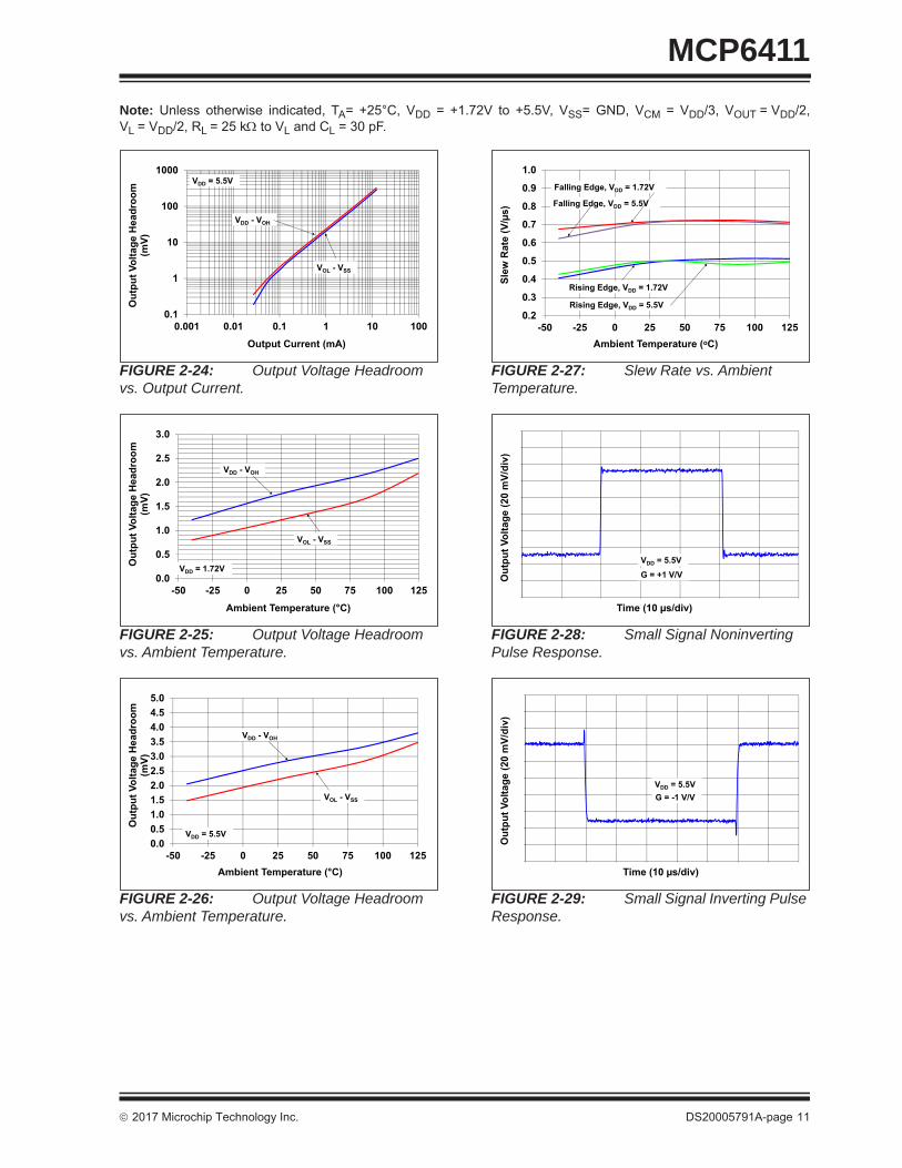
Note: Unless otherwise indicated, TA= +25°C, VDD = +1.72V to +5.5V, VSS= GND, VCM = VDD/3, VOUT = VDD/2,VL = VDD/2, RL = 25 k to VL and CL = 30 pF.FIGURE 2-24: Output Voltage Headroom vs. Output Current.
FIGURE 2-25: Output Voltage Headroom vs. Ambient Temperature.
FIGURE 2-26: Output Voltage Headroom vs. Ambient Temperature.
FIGURE 2-27: Slew Rate vs. Ambient Temperature.
FIGURE 2-28: Small Signal Noninverting Pulse Response.
FIGURE 2-29: Small Signal Inverting Pulse Response.
0.1
1
10
100
1000
0.001 0.01 0.1 1 10 100
Out
put V
olta
ge H
eadr
oom
(m
V)
Output Current (mA)
VDD = 5.5V
VDD - VOH
VOL - VSS
0.0
0.5
1.0
1.5
2.0
2.5
3.0
-50 -25 0 25 50 75 100 125
Out
put V
olta
ge H
eadr
oom
(m
V)
Ambient Temperature (°C)
VDD = 1.72V
VDD - VOH
VOL - VSS
0.00.51.01.52.02.53.03.54.04.55.0
-50 -25 0 25 50 75 100 125
Out
put V
olta
ge H
eadr
oom
(m
V)
Ambient Temperature (°C)
VDD = 5.5V
VDD - VOH
VOL - VSS
0.2
0.3
0.4
0.5
0.6
0.7
0.8
0.9
1.0
-50 -25 0 25 50 75 100 125
Slew
Rat
e (V
/μs)
Ambient Temperature ( C)
Falling Edge, VDD = 5.5V
Falling Edge, VDD = 1.72V
Rising Edge, VDD = 5.5V
Rising Edge, VDD = 1.72V
Out
put V
olta
ge (2
0 m
V/di
v)
Time (10 μs/div)
VDD = 5.5VG = +1 V/V
Out
put V
olta
ge (2
0 m
V/di
v)
Time (10 μs/div)
VDD = 5.5VG = -1 V/V
2017 Microchip Technology Inc. DS20005791A-page 11
MCP6411
Note: Unless otherwise indicated, TA= +25°C, VDD = +1.72V to +5.5V, VSS= GND, VCM = VDD/3, VOUT = VDD/2,VL = VDD/2, RL = 25 k to VL and CL = 30 pF.FIGURE 2-30: Large Signal Noninverting Pulse Response.
FIGURE 2-31: Large Signal Inverting Pulse Response.
FIGURE 2-32: The MCP6411 Device Shows No Phase Reversal.
FIGURE 2-33: Closed Loop Output Impedance vs. Frequency.
FIGURE 2-34: Measured Input Current vs. Input Voltage (below VSS).
FIGURE 2-35: EMIRR vs. Frequency.
0
1
2
3
4
5
6
Out
put V
olta
ge (V
)
Time (0.1 ms/div)
VDD = 5.5VG = +1 V/V
0
1
2
3
4
5
6
Out
put V
olta
ge (V
)
Time (0.1 ms/div)
VDD = 5.5VG = +1 V/V
-1
0
1
2
3
4
5
6
Inpu
t, O
utpu
t Vol
tage
s (V
)
Time (0.1 ms/div)
VDD = 5.5VG = +2 V/V
VOUT
VIN
1
10
100
1000
10000
1.0E+02 1.0E+03 1.0E+04 1.0E+05 1.0E+06
Clo
sed
Loop
Out
put
Impe
danc
e (
)
Frequency (Hz)
GN:101 V/V11 V/V1 V/V
1k 10k 100k 1M 10M
VDD = 2.2V
1E-09
1E-08
0.0000001
0.000001
0.00001
0.0001
0.001
0.01
0.1
-1 -0.8 -0.6 -0.4 -0.2 0
-I IN
(A)
VIN (V)
100m
10m
1m
100μ
10μ
1μ
10n
100n
1n
TA = +125°CTA = +85°CTA = +25°CTA = -40°C
0102030405060708090
100110120
10 100 1000 10000
EM
IRR
(dB
)
Frequency (MHz)
VIN = 316 mVPK VDD = 5.5V
DS20005791A-page 12 2017 Microchip Technology Inc.
MCP6411
Note: Unless otherwise indicated, TA= +25°C, VDD = +1.72V to +5.5V, VSS= GND, VCM = VDD/3, VOUT = VDD/2,VL = VDD/2, RL = 25 k to VL and CL = 30 pF.FIGURE 2-36: EMIRR vs. RF Input Peak-to-Peak Voltage.
0102030405060708090
100110120
0.01 0.1 1
EMIR
R (d
B)
RF Input Peak Voltage (VPK)
EMIRR @ 2400 MHZEMIRR @ 1800 MHZEMIRR @ 900 MHZEMIRR @ 400 MHZ
2017 Microchip Technology Inc. DS20005791A-page 13

MCP6411
NOTES:DS20005791A-page 14 2017 Microchip Technology Inc.
MCP6411
3.0 PIN DESCRIPTIONSDescriptions of the pins are listed in Table 3-1.3.1 Analog OutputsThe output pin is a low-impedance voltage source.
3.2 Analog InputsThe noninverting and inverting inputs arehigh-impedance CMOS inputs with low bias currents.
3.3 Power Supply Pins (VSS, VDD)The positive power supply (VDD) is 1.72V to 5.5Vhigher than the negative power supply (VSS). Fornormal operation, the other pins are at voltagesbetween VSS and VDD.
Typically, these parts are used in a single (positive)supply configuration. In this case, VSS is connected toground and VDD is connected to the supply. VDD willneed bypass capacitors.
TABLE 3-1: PIN FUNCTION TABLEMCP6411
Symbol DescriptionSC70-5, SOT-23-5
1 VOUT Analog Output 2 VSS Negative Power Supply3 VIN+ Noninverting Input 4 VIN– Inverting Input 5 VDD Positive Power Supply
2017 Microchip Technology Inc. DS20005791A-page 15
MCP6411
NOTES:DS20005791A-page 16 2017 Microchip Technology Inc.
MCP6411
4.0 APPLICATION INFORMATIONThe MCP6411 op amp is manufactured usingMicrochip’s state-of-the-art CMOS process. This opamp is unity gain stable and suitable for a wide rangeof general-purpose applications.4.1 Rail-to-Rail Input
4.1.1 PHASE REVERSALThe MCP6411 op amp is designed to prevent phasereversal, when the input pins exceed the supplyvoltages. Figure 2-32 shows the input voltageexceeding the supply voltage with no phase reversal.
4.1.2 INPUT VOLTAGE LIMITSIn order to prevent damage and/or improper operationof the amplifier, the circuit must limit the voltages at theinput pins (see Section 1.1, Absolute MaximumRatings †).
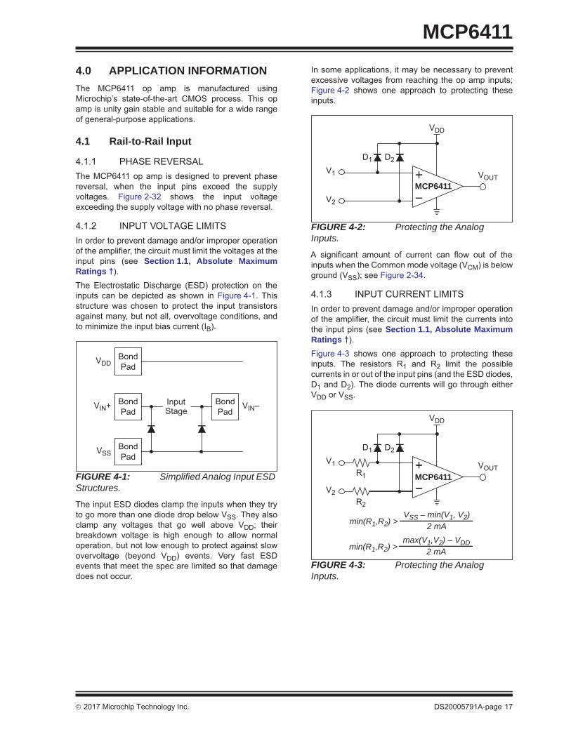
The Electrostatic Discharge (ESD) protection on theinputs can be depicted as shown in Figure 4-1. Thisstructure was chosen to protect the input transistorsagainst many, but not all, overvoltage conditions, andto minimize the input bias current (IB).
FIGURE 4-1: Simplified Analog Input ESD Structures.
The input ESD diodes clamp the inputs when they tryto go more than one diode drop below VSS. They alsoclamp any voltages that go well above VDD; theirbreakdown voltage is high enough to allow normaloperation, but not low enough to protect against slowovervoltage (beyond VDD) events. Very fast ESDevents that meet the spec are limited so that damagedoes not occur.
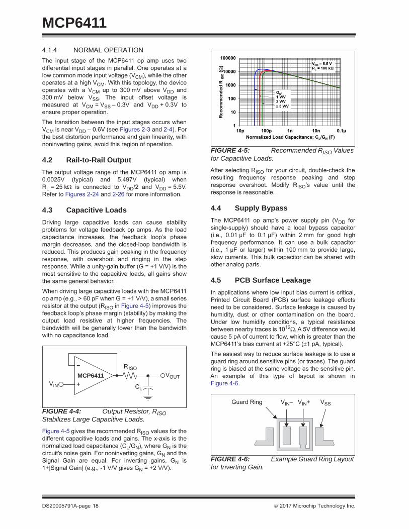
In some applications, it may be necessary to preventexcessive voltages from reaching the op amp inputs;Figure 4-2 shows one approach to protecting theseinputs.
FIGURE 4-2: Protecting the Analog Inputs.
A significant amount of current can flow out of theinputs when the Common mode voltage (VCM) is belowground (VSS); see Figure 2-34.
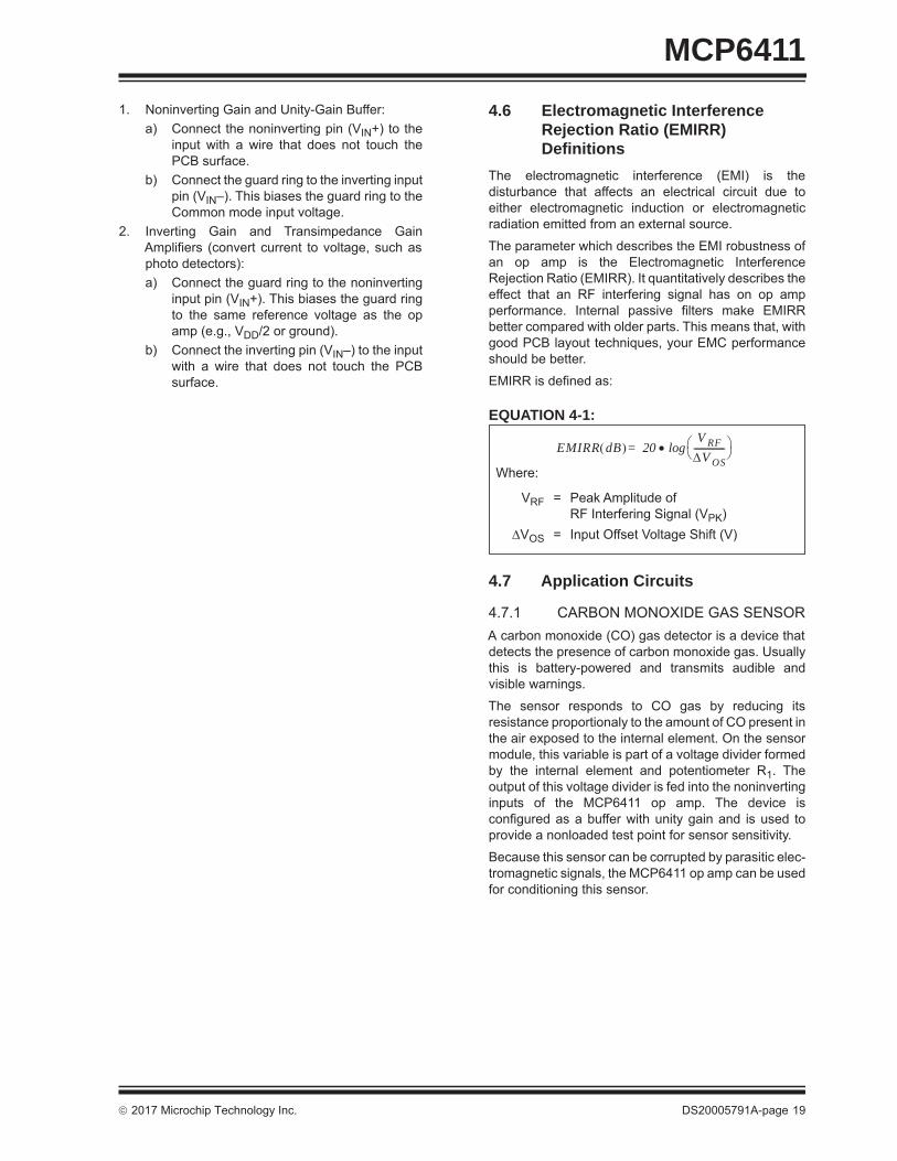
4.1.3 INPUT CURRENT LIMITSIn order to prevent damage and/or improper operationof the amplifier, the circuit must limit the currents intothe input pins (see Section 1.1, Absolute MaximumRatings †).
Figure 4-3 shows one approach to protecting theseinputs. The resistors R1 and R2 limit the possiblecurrents in or out of the input pins (and the ESD diodes,D1 and D2). The diode currents will go through eitherVDD or VSS.
FIGURE 4-3: Protecting the Analog Inputs.
BondPad
BondPad
BondPad
VDD
VIN+
VSS
InputStage
BondPad
VIN–
V1
VDD
D1
V2
D2
MCP6411VOUT
V1R1
VDD
D1
min(R1,R2) > VSS – min(V1, V2)
2 mA
V2R2
D2
MCP6411VOUT
min(R1,R2) > max(V1,V2) – VDD
2 mA
2017 Microchip Technology Inc. DS20005791A-page 17
MCP6411
4.1.4 NORMAL OPERATIONThe input stage of the MCP6411 op amp uses twodifferential input stages in parallel. One operates at alow common mode input voltage (VCM), while the otheroperates at a high VCM. With this topology, the deviceoperates with a VCM up to 300 mV above VDD and300 mV below VSS. The input offset voltage ismeasured at VCM = VSS – 0.3V and VDD + 0.3V toensure proper operation.The transition between the input stages occurs whenVCM is near VDD – 0.6V (see Figures 2-3 and 2-4). Forthe best distortion performance and gain linearity, withnoninverting gains, avoid this region of operation.
4.2 Rail-to-Rail OutputThe output voltage range of the MCP6411 op amp is0.0025V (typical) and 5.497V (typical) whenRL = 25 k is connected to VDD/2 and VDD = 5.5V.Refer to Figures 2-24 and 2-26 for more information.
4.3 Capacitive LoadsDriving large capacitive loads can cause stabilityproblems for voltage feedback op amps. As the loadcapacitance increases, the feedback loop’s phasemargin decreases, and the closed-loop bandwidth isreduced. This produces gain peaking in the frequencyresponse, with overshoot and ringing in the stepresponse. While a unity-gain buffer (G = +1 V/V) is themost sensitive to the capacitive loads, all gains showthe same general behavior.
When driving large capacitive loads with the MCP6411op amp (e.g., > 60 pF when G = +1 V/V), a small seriesresistor at the output (RISO in Figure 4-5) improves thefeedback loop’s phase margin (stability) by making theoutput load resistive at higher frequencies. Thebandwidth will be generally lower than the bandwidthwith no capacitance load.
FIGURE 4-4: Output Resistor, RISO Stabilizes Large Capacitive Loads.
Figure 4-5 gives the recommended RISO values for thedifferent capacitive loads and gains. The x-axis is thenormalized load capacitance (CL/GN), where GN is thecircuit's noise gain. For noninverting gains, GN and theSignal Gain are equal. For inverting gains, GN is1+|Signal Gain| (e.g., -1 V/V gives GN = +2 V/V).
FIGURE 4-5: Recommended RISO Values for Capacitive Loads.
After selecting RISO for your circuit, double-check theresulting frequency response peaking and stepresponse overshoot. Modify RISO’s value until theresponse is reasonable.
4.4 Supply BypassThe MCP6411 op amp’s power supply pin (VDD forsingle-supply) should have a local bypass capacitor(i.e., 0.01 μF to 0.1 μF) within 2 mm for good highfrequency performance. It can use a bulk capacitor(i.e., 1 μF or larger) within 100 mm to provide large,slow currents. This bulk capacitor can be shared withother analog parts.
4.5 PCB Surface LeakageIn applications where low input bias current is critical,Printed Circuit Board (PCB) surface leakage effectsneed to be considered. Surface leakage is caused byhumidity, dust or other contamination on the board.Under low humidity conditions, a typical resistancebetween nearby traces is 1012. A 5V difference wouldcause 5 pA of current to flow, which is greater than theMCP6411’s bias current at +25°C (±1 pA, typical).
The easiest way to reduce surface leakage is to use aguard ring around sensitive pins (or traces). The guardring is biased at the same voltage as the sensitive pin.An example of this type of layout is shown inFigure 4-6.
FIGURE 4-6: Example Guard Ring Layout for Inverting Gain.
VIN
RISOVOUT
CL
–
+MCP6411
100
1000
10000
100000
omm
ende
d R
ISO
(Ω)
GN:1 V/V2 V/V≥ 5 V/V
VDD = 5.5 V RL = 100 k
1
10
1.E-11 1.E-10 1.E-09 1.E-08 1.E-07
Rec
o
Normalized Load Capacitance; CL/GN (F)10p 100p 1n 10n 0.1μ
Guard Ring VIN– VIN+ VSS
DS20005791A-page 18 2017 Microchip Technology Inc.
MCP6411
1. Noninverting Gain and Unity-Gain Buffer:a) Connect the noninverting pin (VIN+) to theinput with a wire that does not touch thePCB surface.
b) Connect the guard ring to the inverting inputpin (VIN–). This biases the guard ring to theCommon mode input voltage.
2. Inverting Gain and Transimpedance GainAmplifiers (convert current to voltage, such asphoto detectors):a) Connect the guard ring to the noninverting
input pin (VIN+). This biases the guard ringto the same reference voltage as the opamp (e.g., VDD/2 or ground).
b) Connect the inverting pin (VIN–) to the inputwith a wire that does not touch the PCBsurface.
4.6 Electromagnetic Interference Rejection Ratio (EMIRR) Definitions
The electromagnetic interference (EMI) is thedisturbance that affects an electrical circuit due toeither electromagnetic induction or electromagneticradiation emitted from an external source.
The parameter which describes the EMI robustness ofan op amp is the Electromagnetic InterferenceRejection Ratio (EMIRR). It quantitatively describes theeffect that an RF interfering signal has on op ampperformance. Internal passive filters make EMIRRbetter compared with older parts. This means that, withgood PCB layout techniques, your EMC performanceshould be better.
EMIRR is defined as:
EQUATION 4-1:
4.7 Application Circuits
4.7.1 CARBON MONOXIDE GAS SENSORA carbon monoxide (CO) gas detector is a device thatdetects the presence of carbon monoxide gas. Usuallythis is battery-powered and transmits audible andvisible warnings.
The sensor responds to CO gas by reducing itsresistance proportionaly to the amount of CO present inthe air exposed to the internal element. On the sensormodule, this variable is part of a voltage divider formedby the internal element and potentiometer R1. Theoutput of this voltage divider is fed into the noninvertinginputs of the MCP6411 op amp. The device isconfigured as a buffer with unity gain and is used toprovide a nonloaded test point for sensor sensitivity.
Because this sensor can be corrupted by parasitic elec-tromagnetic signals, the MCP6411 op amp can be usedfor conditioning this sensor.
EMIRR dB 20V RF
V OS-------------- log=
Where:
VRF = Peak Amplitude of RF Interfering Signal (VPK)
VOS = Input Offset Voltage Shift (V)
2017 Microchip Technology Inc. DS20005791A-page 19
MCP6411
In Figure 4-7, the variable resistor is used to calibratethe sensor in different environments. .FIGURE 4-7: CO Gas Sensor Circuit.
4.7.2 PRESSURE SENSOR AMPLIFIERThe MCP6411 is well-suited for conditioning sensorsignals in battery-powered applications. Many sensorsare configured as Wheatstone bridges. Strain gaugesand pressure sensors are two common examples.
Figure 4-8 shows a strain gauge amplifier, using theMCP6411 Enhanced EMI protection device. Thedifference amplifier with EMI robustness op amp isused to amplify the signal from the Wheatstone bridge.The two op amps, configured as buffers and connectedat outputs of pressure sensors, prevents resistiveloading of the bridge by resistor R1 and R2. ResistorsR1,R2 and R3,R5 need to be chosen with very lowtolerance to match the CMRR.
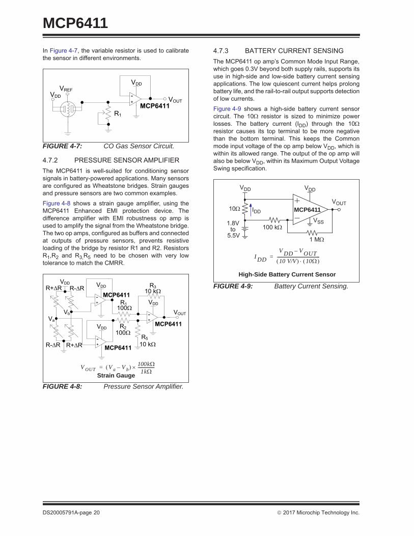
FIGURE 4-8: Pressure Sensor Amplifier.
4.7.3 BATTERY CURRENT SENSINGThe MCP6411 op amp’s Common Mode Input Range,which goes 0.3V beyond both supply rails, supports itsuse in high-side and low-side battery current sensingapplications. The low quiescent current helps prolongbattery life, and the rail-to-rail output supports detectionof low currents.
Figure 4-9 shows a high-side battery current sensorcircuit. The 10 resistor is sized to minimize powerlosses. The battery current (IDD) through the 10resistor causes its top terminal to be more negativethan the bottom terminal. This keeps the Commonmode input voltage of the op amp below VDD, which iswithin its allowed range. The output of the op amp willalso be below VDD, within its Maximum Output VoltageSwing specification.
FIGURE 4-9: Battery Current Sensing.
VDD
+- VOUT
MCP64 1R1
VREFVDD
Strain GaugeV OUT V a V b– 100k
1k----------------=
VDD
R2
+- VOUT
MCP6
R1
R310 k�
R510 k�
100�
100�
VDDR-∆R
R+∆R
Va
Vb
VDD
+-
VDD
+-
MCP64 1
MCP64 1R+∆R
R-∆R
VDD
IDD
100 k
1 M
1.8V
VOUT
High-Side Battery Current Sensor
10
to5.5V
I DDV DD V OUT–
10 V/V 10 ------------------------------------------=
MCP6411
VDD
VSS
DS20005791A-page 20 2017 Microchip Technology Inc.
MCP6411
5.0 DESIGN AIDSMicrochip provides the basic design tools needed forthe MCP6411 op amp.5.1 FilterLab® SoftwareMicrochip’s FilterLab software is an innovative softwaretool that simplifies analog active filter design using opamps. Available at no cost from the Microchip web siteat www.microchip.com/filterlab, the FilterLab designtool provides full schematic diagrams of the filter circuitwith component values. It also outputs the filter circuitin SPICE format, which can be used with the macromodel to simulate the actual filter performance.
5.2 Microchip Advanced Part Selector (MAPS)
MAPS is a software tool that helps semiconductorprofessionals efficiently identify the Microchipdevices that fit a particular design requirement.Available at no cost from the Microchip website atwww.microchip.com/ maps, MAPS is an overallselection tool for Microchip’s product portfolio thatincludes Analog, Memory, MCUs and DSCs. Using thistool, you can define a filter to sort features for aparametric search of devices and export side-by-sidetechnical comparison reports. Helpful links are alsoprovided for data sheets, purchase and sampling ofMicrochip parts.
5.3 Analog Demonstration and Evaluation Boards
Microchip offers a broad spectrum of AnalogDemonstration and Evaluation Boards that aredesigned to help you achieve faster time to market.For a complete listing of these boards and theircorresponding user’s guides and technicalinformation, visit the Microchip web site atwww.microchipdirect.com.
Some boards that are especially useful are:
• MCP6XXX Amplifier Evaluation Board 1• MCP6XXX Amplifier Evaluation Board 2• MCP6XXX Amplifier Evaluation Board 3• MCP6XXX Amplifier Evaluation Board 4• Active Filter Demo Board Kit• 5/6-Pin SOT-23 Evaluation Board, P/N VSUPEV2
5.4 Application NotesThe following Microchip Analog Design Note andApplication Notes are available on the Microchip website at www.microchip.com/appnotes, and arerecommended as supplemental reference resources.
• ADN003 – “Select the Right Operational Amplifier for your Filtering Circuits”, DS21821
• AN722 – “Operational Amplifier Topologies and DC Specifications”, DS00722
• AN723 – “Operational Amplifier AC Specifications and Applications”, DS00723
• AN884 – “Driving Capacitive Loads With Op Amps”, DS00884
• AN990 – “Analog Sensor Conditioning Circuits – An Overview”, DS00990
• AN1177 – “Op Amp Precision Design: DC Errors”, DS01177
• AN1228 – “Op Amp Precision Design: Random Noise”, DS01228
• AN1297 – “Microchip’s Op Amp SPICE Macro Models”, DS01297
• AN1332: “Current Sensing Circuit Concepts and Fundamentals”’ DS01332
• AN1494: “Using MCP6491 Op Amps for Photode-tection Applications”’ DS01494
These application notes and others are listed in thedesign guide:
• “Signal Chain Design Guide”, DS21825
2017 Microchip Technology Inc. DS20005791A-page 21

MCP6411
NOTES:DS20005791A-page 22 2017 Microchip Technology Inc.
MCP6411
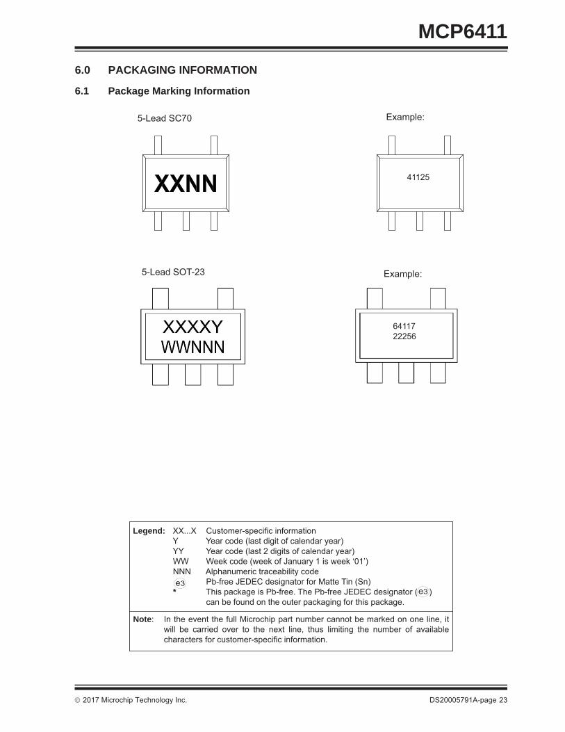
6.0 PACKAGING INFORMATION6.1 Package Marking Information
Example:
Legend: XX...X Customer-specific informationY Year code (last digit of calendar year)YY Year code (last 2 digits of calendar year)WW Week code (week of January 1 is week ‘01’)NNN Alphanumeric traceability code Pb-free JEDEC designator for Matte Tin (Sn)* This package is Pb-free. The Pb-free JEDEC designator ( )
can be found on the outer packaging for this package.
Note: In the event the full Microchip part number cannot be marked on one line, itwill be carried over to the next line, thus limiting the number of availablecharacters for customer-specific information.
3e
3e
Example: 5-Lead SOT-23
5-Lead SC70
41125
6411722256
2017 Microchip Technology Inc. DS20005791A-page 23
MCP6411
DS20005791A-page 24 2017 Microchip Technology Inc.
MCP6411
2017 Microchip Technology Inc. DS20005791A-page 25
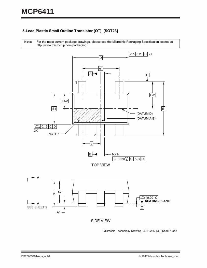
MCP6411
0.15 C D2X
NOTE 1 1 2
N
TOP VIEW
SIDE VIEW
Microchip Technology Drawing C04-028D [OT] Sheet 1 of
For the most current package drawings, please see the Microchip Packaging Specification located athttp://www.microchip.com/packaging
Note:
0.20 C
C
SEATING PLANE
A A2
A1
e
NX bB0.20 C A-B D
e1
D
E1
E1/2
E/2
E
DA
0.20 C 2X
(DATUM D)(DATUM A-B)
A
ASEE SHEET 2
5-Lead Plastic Small Outline Transistor (OT) [SOT23]
DS20005791A-page 26 2017 Microchip Technology Inc.
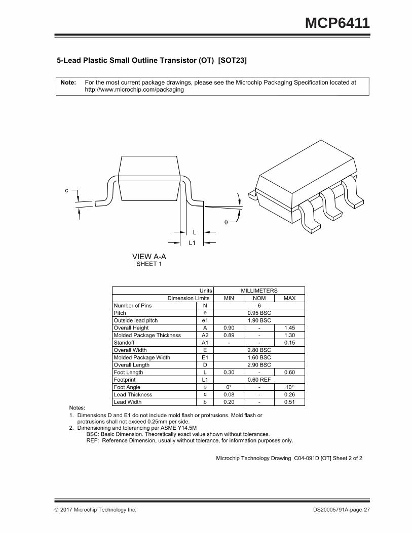
MCP6411
Microchip Technology Drawing C04-091D [OT] Sheet 2 of
For the most current package drawings, please see the Microchip Packaging Specification located athttp://www.microchip.com/packaging
Note:
c
L
L1
VIEW A-ASHEET 1
5-Lead Plastic Small Outline Transistor (OT) [SOT23]
protrusions shall not exceed 0.25mm per side.1.
BSC: Basic Dimension. Theoretically exact value shown without tolerances.2.
Foot Angle
Number of PinsPitchOutside lead pitchOverall HeightMolded Package ThicknessStandoffOverall WidthMolded Package WidthOverall LengthFoot LengthFootprint
Lead ThicknessLead Width
Notes:
L1
bc
Dimension Limits
EE1DL
e1AA2A1
Units
Ne
0°0.080.20 -
--
10°0.260.51
MILLIMETERS
0.95 BSC1.90 BSC
0.30
0.900.89
-
0.60 REF
2.90 BSC-
2.80 BSC1.60 BSC
--
-
MIN6
NOM
1.451.300.15
0.60
MAX
REF: Reference Dimension, usually without tolerance, for information purposes only.
Dimensions D and E1 do not include mold flash or protrusions. Mold flash or
Dimensioning and tolerancing per ASME Y14.5M
2017 Microchip Technology Inc. DS20005791A-page 27
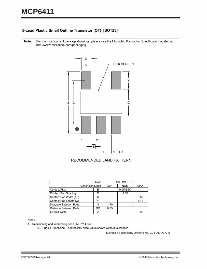
MCP6411
RECOMMENDED LAND PATTERN
5-Lead Plastic Small Outline Transistor (OT) [SOT23]
For the most current package drawings, please see the Microchip Packaging Specification located athttp://www.microchip.com/packaging
Note:
BSC: Basic Dimension. Theoretically exact value shown without tolerances.
Notes:1. Dimensioning and tolerancing per ASME Y14.5M
Microchip Technology Drawing No. C04-2091A [OT]
Dimension Limits
Contact Pad Length (X5)
Overall Width
Distance Between Pads
Contact Pad Width (X5)
Contact PitchContact Pad Spacing
3.90
1.10G
Z
Y1.70
0.60
MAXMIN
CX
E
UnitsNOM
0.95 BSC2.80
MILLIMETERS
Distance Between Pads GX 0.35
1
5
X
Y
Z C
E
GX
G
2
SILK SCREEN
DS20005791A-page 28 2017 Microchip Technology Inc.
MCP6411
APPENDIX A: REVISION HISTORYRevision A (June 2017)• Original Release of this Document.
2017 Microchip Technology Inc. DS20005791A-page 29

MCP6411
NOTES:DS20005791A-page 30 2017 Microchip Technology Inc.
MCP6411
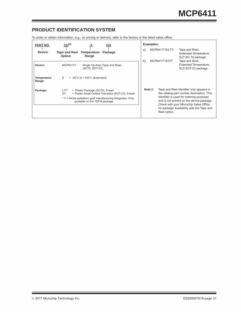
PRODUCT IDENTIFICATION SYSTEMTo order or obtain information, e.g., on pricing or delivery, refer to the factory or the listed sales office.Device: MCP6411T: Single Op Amp (Tape and Reel)(SC70, SOT-23)
Temperature Range:
E = -40°C to +125°C (Extended)
Package: LTY* = Plastic Package (SC70), 5-leadOT = Plastic Small Outline Transistor (SOT-23), 5-lead
* Y = Nickel palladium gold manufacturing designator. Only available on the TDFN package.
PART NO. -X /XX
PackageTemperatureRange
Device
Examples:a) MCP6411T-E/LTY: Tape and Reel,
Extended Temperature,5LD SC-70 package
b) MCP6411T-E/OT: Tape and Reel,Extended Temperature,5LD SOT-23 package
[X](1)
Tape and ReelOption
Note 1: Tape and Reel identifier only appears in the catalog part number description. This identifier is used for ordering purposes and is not printed on the device package. Check with your Microchip Sales Office for package availability with the Tape and Reel option.
2017 Microchip Technology Inc. DS20005791A-page 31

MCP6411
NOTES:DS20005791A-page 32 2017 Microchip Technology Inc.
Note the following details of the code protection feature on Microchip devices:• Microchip products meet the specification contained in their particular Microchip Data Sheet.
• Microchip believes that its family of products is one of the most secure families of its kind on the market today, when used in the intended manner and under normal conditions.
• There are dishonest and possibly illegal methods used to breach the code protection feature. All of these methods, to our knowledge, require using the Microchip products in a manner outside the operating specifications contained in Microchip’s Data Sheets. Most likely, the person doing so is engaged in theft of intellectual property.
• Microchip is willing to work with the customer who is concerned about the integrity of their code.
• Neither Microchip nor any other semiconductor manufacturer can guarantee the security of their code. Code protection does not mean that we are guaranteeing the product as “unbreakable.”
Code protection is constantly evolving. We at Microchip are committed to continuously improving the code protection features of ourproducts. Attempts to break Microchip’s code protection feature may be a violation of the Digital Millennium Copyright Act. If such actsallow unauthorized access to your software or other copyrighted work, you may have a right to sue for relief under that Act.
Information contained in this publication regarding deviceapplications and the like is provided only for your convenienceand may be superseded by updates. It is your responsibility toensure that your application meets with your specifications.MICROCHIP MAKES NO REPRESENTATIONS ORWARRANTIES OF ANY KIND WHETHER EXPRESS ORIMPLIED, WRITTEN OR ORAL, STATUTORY OROTHERWISE, RELATED TO THE INFORMATION,INCLUDING BUT NOT LIMITED TO ITS CONDITION,QUALITY, PERFORMANCE, MERCHANTABILITY ORFITNESS FOR PURPOSE. Microchip disclaims all liabilityarising from this information and its use. Use of Microchipdevices in life support and/or safety applications is entirely atthe buyer’s risk, and the buyer agrees to defend, indemnify andhold harmless Microchip from any and all damages, claims,suits, or expenses resulting from such use. No licenses areconveyed, implicitly or otherwise, under any Microchipintellectual property rights unless otherwise stated.
2017 Microchip Technology Inc.
Microchip received ISO/TS-16949:2009 certification for its worldwide headquarters, design and wafer fabrication facilities in Chandler and Tempe, Arizona; Gresham, Oregon and design centers in California and India. The Company’s quality system processes and procedures are for its PIC® MCUs and dsPIC® DSCs, KEELOQ® code hopping devices, Serial EEPROMs, microperipherals, nonvolatile memory and analog products. In addition, Microchip’s quality system for the design and manufacture of development systems is ISO 9001:2000 certified.
TrademarksThe Microchip name and logo, the Microchip logo, AnyRate, AVR, AVR logo, AVR Freaks, BeaconThings, BitCloud, CryptoMemory, CryptoRF, dsPIC, FlashFlex, flexPWR, Heldo, JukeBlox, KEELOQ, KEELOQ logo, Kleer, LANCheck, LINK MD, maXStylus, maXTouch, MediaLB, megaAVR, MOST, MOST logo, MPLAB, OptoLyzer, PIC, picoPower, PICSTART, PIC32 logo, Prochip Designer, QTouch, RightTouch, SAM-BA, SpyNIC, SST, SST Logo, SuperFlash, tinyAVR, UNI/O, and XMEGA are registered trademarks of Microchip Technology Incorporated in the U.S.A. and other countries.
ClockWorks, The Embedded Control Solutions Company, EtherSynch, Hyper Speed Control, HyperLight Load, IntelliMOS, mTouch, Precision Edge, and Quiet-Wire are registered trademarks of Microchip Technology Incorporated in the U.S.A.
Adjacent Key Suppression, AKS, Analog-for-the-Digital Age, Any Capacitor, AnyIn, AnyOut, BodyCom, chipKIT, chipKIT logo, CodeGuard, CryptoAuthentication, CryptoCompanion, CryptoController, dsPICDEM, dsPICDEM.net, Dynamic Average Matching, DAM, ECAN, EtherGREEN, In-Circuit Serial Programming, ICSP, Inter-Chip Connectivity, JitterBlocker, KleerNet, KleerNet logo, Mindi, MiWi, motorBench, MPASM, MPF, MPLAB Certified logo, MPLIB, MPLINK, MultiTRAK, NetDetach, Omniscient Code Generation, PICDEM, PICDEM.net, PICkit, PICtail, PureSilicon, QMatrix, RightTouch logo, REAL ICE, Ripple Blocker, SAM-ICE, Serial Quad I/O, SMART-I.S., SQI, SuperSwitcher, SuperSwitcher II, Total Endurance, TSHARC, USBCheck, VariSense, ViewSpan, WiperLock, Wireless DNA, and ZENA are trademarks of Microchip Technology Incorporated in the U.S.A. and other countries.
SQTP is a service mark of Microchip Technology Incorporated in the U.S.A.
Silicon Storage Technology is a registered trademark of Microchip Technology Inc. in other countries.
GestIC is a registered trademark of Microchip Technology Germany II GmbH & Co. KG, a subsidiary of Microchip Technology Inc., in other countries.
All other trademarks mentioned herein are property of their respective companies.
© 2017, Microchip Technology Incorporated, All Rights Reserved.
ISBN: 978-1-5224-1837-5
DS20005791A-page 33
DS20005791A-page 34 2017 Microchip Technology Inc.
AMERICASCorporate Office2355 West Chandler Blvd.Chandler, AZ 85224-6199Tel: 480-792-7200 Fax: 480-792-7277Technical Support: http://www.microchip.com/supportWeb Address: www.microchip.comAtlantaDuluth, GA Tel: 678-957-9614 Fax: 678-957-1455Austin, TXTel: 512-257-3370 BostonWestborough, MA Tel: 774-760-0087 Fax: 774-760-0088ChicagoItasca, IL Tel: 630-285-0071 Fax: 630-285-0075DallasAddison, TX Tel: 972-818-7423 Fax: 972-818-2924DetroitNovi, MI Tel: 248-848-4000Houston, TX Tel: 281-894-5983IndianapolisNoblesville, IN Tel: 317-773-8323Fax: 317-773-5453Tel: 317-536-2380Los AngelesMission Viejo, CA Tel: 949-462-9523Fax: 949-462-9608Tel: 951-273-7800 Raleigh, NC Tel: 919-844-7510New York, NY Tel: 631-435-6000San Jose, CA Tel: 408-735-9110Tel: 408-436-4270Canada - TorontoTel: 905-695-1980 Fax: 905-695-2078
ASIA/PACIFICAsia Pacific OfficeSuites 3707-14, 37th FloorTower 6, The GatewayHarbour City, KowloonHong KongTel: 852-2943-5100Fax: 852-2401-3431Australia - SydneyTel: 61-2-9868-6733Fax: 61-2-9868-6755China - BeijingTel: 86-10-8569-7000 Fax: 86-10-8528-2104China - ChengduTel: 86-28-8665-5511Fax: 86-28-8665-7889China - ChongqingTel: 86-23-8980-9588Fax: 86-23-8980-9500China - DongguanTel: 86-769-8702-9880 China - GuangzhouTel: 86-20-8755-8029 China - HangzhouTel: 86-571-8792-8115 Fax: 86-571-8792-8116China - Hong Kong SARTel: 852-2943-5100 Fax: 852-2401-3431China - NanjingTel: 86-25-8473-2460Fax: 86-25-8473-2470China - QingdaoTel: 86-532-8502-7355Fax: 86-532-8502-7205China - ShanghaiTel: 86-21-3326-8000 Fax: 86-21-3326-8021China - ShenyangTel: 86-24-2334-2829Fax: 86-24-2334-2393China - ShenzhenTel: 86-755-8864-2200 Fax: 86-755-8203-1760China - WuhanTel: 86-27-5980-5300Fax: 86-27-5980-5118China - XianTel: 86-29-8833-7252Fax: 86-29-8833-7256
ASIA/PACIFICChina - XiamenTel: 86-592-2388138 Fax: 86-592-2388130China - ZhuhaiTel: 86-756-3210040 Fax: 86-756-3210049India - BangaloreTel: 91-80-3090-4444 Fax: 91-80-3090-4123India - New DelhiTel: 91-11-4160-8631Fax: 91-11-4160-8632India - PuneTel: 91-20-3019-1500Japan - OsakaTel: 81-6-6152-7160 Fax: 81-6-6152-9310Japan - TokyoTel: 81-3-6880- 3770 Fax: 81-3-6880-3771Korea - DaeguTel: 82-53-744-4301Fax: 82-53-744-4302Korea - SeoulTel: 82-2-554-7200Fax: 82-2-558-5932 or 82-2-558-5934Malaysia - Kuala LumpurTel: 60-3-6201-9857Fax: 60-3-6201-9859Malaysia - PenangTel: 60-4-227-8870Fax: 60-4-227-4068Philippines - ManilaTel: 63-2-634-9065Fax: 63-2-634-9069SingaporeTel: 65-6334-8870Fax: 65-6334-8850Taiwan - Hsin ChuTel: 886-3-5778-366Fax: 886-3-5770-955Taiwan - KaohsiungTel: 886-7-213-7830Taiwan - TaipeiTel: 886-2-2508-8600 Fax: 886-2-2508-0102Thailand - BangkokTel: 66-2-694-1351Fax: 66-2-694-1350
EUROPEAustria - WelsTel: 43-7242-2244-39Fax: 43-7242-2244-393Denmark - CopenhagenTel: 45-4450-2828 Fax: 45-4485-2829Finland - EspooTel: 358-9-4520-820France - ParisTel: 33-1-69-53-63-20 Fax: 33-1-69-30-90-79France - Saint CloudTel: 33-1-30-60-70-00 Germany - GarchingTel: 49-8931-9700Germany - HaanTel: 49-2129-3766400Germany - HeilbronnTel: 49-7131-67-3636Germany - KarlsruheTel: 49-721-625370Germany - MunichTel: 49-89-627-144-0 Fax: 49-89-627-144-44Germany - RosenheimTel: 49-8031-354-560Israel - Ra’anana Tel: 972-9-744-7705Italy - Milan Tel: 39-0331-742611 Fax: 39-0331-466781Italy - PadovaTel: 39-049-7625286 Netherlands - DrunenTel: 31-416-690399 Fax: 31-416-690340Norway - TrondheimTel: 47-7289-7561Poland - WarsawTel: 48-22-3325737 Romania - BucharestTel: 40-21-407-87-50Spain - MadridTel: 34-91-708-08-90Fax: 34-91-708-08-91Sweden - GothenbergTel: 46-31-704-60-40Sweden - StockholmTel: 46-8-5090-4654UK - WokinghamTel: 44-118-921-5800Fax: 44-118-921-5820
Worldwide Sales and Service
11/07/16