25-W Filter-Free Mono Class-D Audio Power Amplifier with Speaker ...
Upload
phungxuyenCategory
view
219download
0
General DescriptionThe MAX9768 mono 10W Class D speaker amplifier pro-vides high-quality, efficient audio power with an integrated volume control function.The MAX9768 features a 64-step dual-mode (analog or digitally programmable) volume control and mute function. The audio amplifier operates from a 4.5V to 14V single supply and can deliver up to 10W into an 8Ω speaker with a 14V supply.A selectable spread-spectrum mode reduces EMI-radiated emissions, allowing the device to pass EMC testing with ferrite bead filters and cable lengths up to 1m. The MAX9768 can be synchronized to an external clock, allowing synchronization of multiple Class D amplifiers.The MAX9768 features high 77dB PSRR, low 0.08% THD+N, and SNR up to 97dB. Robust short-circuit and thermal-overload protection prevent device damage during a fault condition. The MAX9768 is available in a 24-pin thin QFN-EP (4mm x 4mm x 0.8mm) package and is specified over the extended -40°C to +85°C temperature range.
Applications Notebook Computers Flat-Panel Displays Multimedia Monitors GPS Navigation Systems Security/Personal Mobile Radio
Features 10W Output (8Ω, PVDD = 14V, THD+N = 10%) Spread-Spectrum Modulation Meets EN55022B EMC with Ferrite Bead Filters Amplifier Operation from 4.5V to 14V Supply 64-Step Integrated Volume Control (I2C or Analog) Low 0.08% THD+N (RL = 8Ω, POUT = 6W) High 77dB PSRR Two tON Times Offered
• MAX9768—220ms• MAX9768B—15ms
Low-Power Shutdown Mode (0.5μA) Short-Circuit and Thermal-Overload Protection
19-0854; Rev 3; 12/17
Pin Configuration located toward end of data sheet.
Ordering Information located at end of data sheet.
MUTE
SHDN
SPEAKERAUDIOINPUT
FILTERLESSCLASS DSPEAKEROUTPUT
ANALOG ORI2C VOLUME
CONTROL
3.3V 4.5V TO 14V
MAX9768
MAX9768 EMI WITH FERRITE BEAD FILTERS(VDD = 12V, 1m CABLE, 8Ω LOAD)
FREQUENCY (MHz)900800100 200 300 500 600400 700
5
10
15
20
AMPL
ITUD
E (d
BV/m
)
25
30
35
40
00 1000
OVER 20dB MARGINTO EN55022B LIMIT
MAX9768 10W Mono Class D Speaker Amplifier with Volume Control
Simplified Block Diagram
EVALUATION KIT AVAILABLE

PVDD to PGND ......................................................-0.3V to +16VVDD to GND ............................................................-0.3V to +4VSCLK, SDA/VOL to GND ........................................-0.3V to +4VFB, SYNCOUT ......................................... -0.3V to (VDD + 0.3V)BOOT_ to OUT_......................................................-0.3V to +4VOUT_ to GND .........................................-0.3V to (PVDD + 0.3V)PGND to GND ......................................................-0.3V to +0.3VAny Other Pin to GND .............................................-0.3V to +4VOUT_ Short-Circuit Duration .....................................ContinuousContinuous Current (PVDD, PGND, OUT_) .........................2.2AContinuous Input Current (Any Other Pin) .......................±20mAContinuous Input Current (FB_) .......................................±60mA
Continuous Power Dissipation (TA = +70°C)Single-Layer Board:
24-Pin Thin QFN 4mm x 4mm, (derate 20.8mW/°C above +70°C) ................................1.67W
Multilayer Board: 24-Pin Thin QFN 4mm x 4mm, (derate 27.8mW/°C above +70°C) ................................2.22W
θJA, Single-Layer Board ..................................................48°C/WθJA, Multilayer Board .......................................................36°C/WOperating Temperature Range ........................... -40°C to +85°CStorage Temperature Range ............................ -65°C to +150°CLead Temperature (soldering, 10s) .................................+300°C
(PVDD = 12V, VDD = 3.3V, VGND = VPGND = 0, VSHDN = VDD, VMUTE = 0; Max volume setting; speaker load resistor connected between OUT+ and OUT-, RL = ∞, unless otherwise noted. CBIAS = 2.2μF, C1 = C2 = 0.1μF, CIN = 0.47μF, RIN = 20kΩ, RF = 30kΩ, SSM mode. Filterless modulation mode (see the Functional Diagram/Typical Application Circuit). TA = TMIN to TMAX, unless otherwise noted. Typical values are at TA = +25°C.) (Note 1)
PARAMETER SYMBOL CONDITIONS MIN TYP MAX UNITSGENERALSpeaker Supply Voltage Range PVDD Inferred from PSRR test 4.5 14.0 V
Supply Voltage Range VDD Inferred from PSRR and UVLO test 2.7 3.6 V
Quiescent CurrentIVDD 7 14.2
mAIPVDD
Filterless modulation 4 7.6Classic PWM modulation 4 7.6
Shutdown Current ISHDN ISHDN = IPVDD + IDD, SHDN = GND, TA = +25°C 0.5 50 µA
Output Offset VOSFilterless modulation, VMUTE = VDD, TA = +25°C ±2 ±12.5
mVFilterless modulation, VMUTE = 0V, TA = +25°C ±2 ±14
Turn-On Time tONMAX9768 220
msMAX9768B 15
Common-Mode Bias Voltage VBIAS 1.5 V
Input Amplifier Output-Voltage Swing High VOH
Specified asVDD - VOH
RL = 2kΩ connect to 1.5V 3.6 100 mV
Input Amplifier Output-Voltage Swing Low VOL
Specified asVOL - GND RL = 2kΩ connect to 1.5V 6 50 mV
Input Amplifier OutputShort-Circuit Current Limit ±60 mA
Input Amplifier Gain-Bandwidth Product GBW 1.8 MHz
SPEAKER AMPLIFIERS
Internal Gain AVMAXMax volume setting; from FB to amplifier outputs |(OUT+) - (OUT-)|; excludes external gain resistors 29.27 30.1 31.00 dB
MAX9768 10W Mono Class D Speaker Amplifier with Volume Control
www.maximintegrated.com Maxim Integrated 2
Absolute Maximum Ratings
Stresses beyond those listed under “Absolute Maximum Ratings” may cause permanent damage to the device. These are stress ratings only, and functional operation of the device at these or any other conditions beyond those indicated in the operational sections of the specifications is not implied. Exposure to absolute maximum rating conditions for extended periods may affect device reliability.
Electrical Characteristics

((PVDD = 12V, VDD = 3.3V, VGND = VPGND = 0, VSHDN = VDD, VMUTE = 0; Max volume setting; speaker load resistor connected between OUT+ and OUT-, RL = ∞, unless otherwise noted. CBIAS = 2.2μF, C1 = C2 = 0.1μF, CIN = 0.47μF, RIN = 20kΩ, RF = 30kΩ, SSM mode. Filterless modulation mode (see the Functional Diagram/Typical Application Circuit). TA = TMIN to TMAX, unless otherwise noted. Typical values are at TA = +25°C.) (Note 1)
PARAMETER SYMBOL CONDITIONS MIN TYP MAX UNITS
Efficiency (Note 2) η POUT = 8W, fIN = 1kHz, RL = 8Ω
Filterless modulation 87%
Classic PWM modulation 85
Output Power (Note 2) POUT
PVDD = 5V
RL = 8Ω, THD+N = 1%, filterless modulation 1.3
W
RL = 8Ω, THD+N = 10%, filterless modulation 1.7
PVDD = 12V
RL = 8Ω, THD+N = 10%, classic PWM modulation 9
RL = 8Ω, THD+N = 10%, filterless modulation 9
PVDD = 14V
RL = 8Ω, THD+N = 10%, classic PWM modulation 10
RL = 8Ω, THD+N = 10%, filterless modulation 10
Soft Output Current Limit ILIM 1.75 2 AHard Output Current Limit ISC 2.5 A
Total Harmonic Distortion Plus Noise (Note 2) THD+N f = 1kHz, RL = 8Ω,
POUT = 5WFilterless modulation 0.09
%Classic PWM modulation 0.08
Signal-to-Noise Ratio(Note 2) SNR
0dB = 8W, RL = 8Ω, BW = 22Hz to 22kHz, filterless modulation mode
UnweightedFFM 94
dB
SSM 93
A-weightedFFM 97SSM 97
0dB = 8W, RL = 8Ω, BW = 22Hz to 22kHz, classic PWM modulation
UnweightedFFM 93SSM 89
A-weightedFFM 97SSM 91
MUTE Attenuation (Note 3) 0dB = 8W, f = 1kHz 115 dB
Power-Supply Rejection Ratio PSRR
VDD = 2.7V to 3.6V, filterless modulation,TA = +25°C 52 68
dBPVDD = 4.5V to 14V, filterless modulation,TA = +25°C 67 84
f = 1kHz, VRIPPLE = 200mVP-P on PVDD 77f = 1kHz, VRIPPLE = 100mVP-P on VDD 60
Oscillator Frequency fOCS
SYNC = GND 1060 1200 1320
kHzSYNC = unconnected 1296 1440 1584
SYNC = VDD (spread-spectrum modulation mode)
1200 ±30
MAX9768 10W Mono Class D Speaker Amplifier with Volume Control
www.maximintegrated.com Maxim Integrated 3
Electrical Characteristics (continued)
((PVDD = 12V, VDD = 3.3V, VGND = VPGND = 0, VSHDN = VDD, VMUTE = 0; Max volume setting; speaker load resistor connected between OUT+ and OUT-, RL = ∞, unless otherwise noted. CBIAS = 2.2μF, C1 = C2 = 0.1μF, CIN = 0.47μF, RIN = 20kΩ, RF = 30kΩ, SSM mode. Filterless modulation mode (see the Functional Diagram/Typical Application Circuit). TA = TMIN to TMAX, unless otherwise noted. Typical values are at TA = +25°C.) (Note 1)
PARAMETER SYMBOL CONDITIONS MIN TYP MAX UNITS
Class D Switching Frequency
SYNC = GND 265 300 330
kHzSYNC = unconnected 324 360 396SYNC = VDD (spread-spectrum modulation mode)
300±7.5
SYNC Frequency Lock Range 1000 1600 kHz
Minimum SYNC Frequency Lock Duty Cycle 40 %
Maximum SYNC Frequency Lock Duty Cycle 60 %
Gain Matching Full volume (ideal matching for RIN and RF) 2 %
Click-and-Pop Level (Note 2) KCP
Peak voltage, 32 samples per second, A-weighted, RIN x CIN ≤ 10ms to guarantee clickless/popless operation
Into shutdown 52.6
dBVOut of shutdown 48Into mute 67Out of mute 57
Input Impedance DC volume control mode (SDA/VOL) 100 MΩInput Hysteresis DC volume control mode (SDA/VOL) 11 mV9.5dB Gain Voltage DC volume control mode (SDA/VOL) 0.1 x VDD VFull Mute Voltage DC volume control mode (SDA/VOL) 0.9 x VDD VDIGITAL INPUTS (SHDN, MUTE, ADDR1, ADDR2, SYNC)
Input-Voltage High VIHSYNC 2.33
VAll other pins 0.7 x VDD
Input-Voltage Low VILSYNC 0.8
VAll other pins 0.3 x VDD
Input Leakage CurrentISYNC TA = +25°C ±7.5 ±13
µAILK All other digital inputs, TA = +25°C ±1
DIGITAL OUTPUT (SYNCOUT)Output-Voltage High Load = 1mA VDD - 0.3 VOutput-Voltage Low Load = 1mA 0.3 VRise/Fall Time CL = 10pF 5 ns
MAX9768 10W Mono Class D Speaker Amplifier with Volume Control
www.maximintegrated.com Maxim Integrated 4
Electrical Characteristics (continued)

((PVDD = 12V, VDD = 3.3V, VGND = VPGND = 0, VSHDN = VDD, VMUTE = 0; Max volume setting; speaker load resistor connected between OUT+ and OUT-, RL = ∞, unless otherwise noted. CBIAS = 2.2μF, C1 = C2 = 0.1μF, CIN = 0.47μF, RIN = 20kΩ, RF = 30kΩ, SSM mode. Filterless modulation mode (see the Functional Diagram/Typical Application Circuit). TA = TMIN to TMAX, unless otherwise noted. Typical values are at TA = +25°C.) (Note 1)
PARAMETER SYMBOL CONDITIONS MIN TYP MAX UNITSTHERMAL PROTECTIONThermal Shutdown Threshold 150 °C
Thermal Shutdown Hysteresis 15 °C
DIGITAL INPUTS (SCLK, SDA/VOL)Input-Voltage High VIH 0.7 x VDD VInput-Voltage Low VIL 0.3 x VDD VInput High Leakage Current IIH VIN = VDD, TA = +25°C ±1 µAInput Low Leakage Current IIL VIN = GND, TA = +25°C ±1 µAInput Hysteresis 0.1 x VDD VInput Capacitance CIN 5 pFDIGITAL OUTPUTS (SDA/VOL)Output High Current IOH VOH = VDD 1 µAOutput Low Voltage VOL IOL = 3mA 0.4 VI2C TIMING CHARACTERISTICS (Figure 3)Serial Clock fSCL 400 kHz
Bus Free Time Between a STOP and STARTCondition
tBUF 1.3 µs
Hold Time (Repeated) START Condition tHD,STA 0.6 µs
Repeated START Condition Setup Time tSU,STA 0.6 µs
STOP Condition Setup Time tSU,STO 0.6 µsData Hold Time tHD,DAT 0 0.9 µsData Setup Time tSU,DAT 100 nsSCL Clock Low Period tLOW 1.3 µsSCL Clock High Period tHIGH 0.6 µs
Rise Time of SDA and SCL, Receiving tR (Note 4) 20 +
0.1Cb 300 ns
Fall Time of SDA and SCL, Receiving tF (Note 4) 20 +
0.1Cb 300 ns
MAX9768 10W Mono Class D Speaker Amplifier with Volume Control
www.maximintegrated.com Maxim Integrated 5
Electrical Characteristics (continued)
((PVDD = 12V, VDD = 3.3V, VGND = VPGND = 0, VSHDN = VDD, VMUTE = 0; Max volume setting; speaker load resistor connected between OUT+ and OUT-, RL = ∞, unless otherwise noted. CBIAS = 2.2μF, C1 = C2 = 0.1μF, CIN = 0.47μF, RIN = 20kΩ, RF = 30kΩ, SSM mode. Filterless modulation mode (see the Functional Diagram/Typical Application Circuit). TA = TMIN to TMAX, unless otherwise noted. Typical values are at TA = +25°C.) (Note 1)
Note 1: All devices are 100% production tested at TA = +25°C. All temperature limits are guaranteed by design.Note 2: Testing performed with a resistive load in series with an inductor to simulate an actual speaker load. For RL = 8Ω, L = 68μH.Note 3: Device muted by either asserting MUTE or minimum VOL setting.Note 4: Cb = total capacitance of one bus line in pF.
((PVDD = 12V, VDD = 3.3V, VGND = VPGND = 0, VMUTE = 0; 0dB volume setting; all speaker load resistors connected between OUT+ and OUT-, RL = 8Ω, unless otherwise noted. CBIAS = 2.2μF, C1 = C2 = 0.1μF, CIN = 0.47μF, RIN = 20kΩ, RFB = 30kΩ, spread-spectrum modulation mode.)
PARAMETER SYMBOL CONDITIONS MIN TYP MAX UNITSFall Time of SDA, Transmitting tF (Note 4) 20 +
0.1Cb 250 ns
Pulse Width of Spike Suppressed tSP 0 50 ns
Capacitive Load for Each Bus Line Cb 400 pF
TOTAL HARMONIC DISTORTIONPLUS NOISE vs. FREQUENCY
MAX
9768
toc0
2
FREQUENCY (Hz)
THD+
N (%
)
10k1k100
0.1
1
10
0.0110 100k
PVDD = 12VRL = 8ΩPWM MODE
OUTPUT POWER = 5W
OUTPUT POWER = 2W
TOTAL HARMONIC DISTORTIONPLUS NOISE vs. FREQUENCY
MAX
9768
toc0
3
FREQUENCY (Hz)
THD+
N (%
)
10k1k100
0.1
0.01
1
10
0.00110 100k
PVDD = 5VRL = 8ΩFILTERLESS MODULATION
OUTPUT POWER = 1W
OUTPUT POWER = 300mW
TOTAL HARMONIC DISTORTIONPLUS NOISE vs. FREQUENCY
MAX
9768
toc0
1
FREQUENCY (Hz)
THD+
N (%
)
10k1k100
0.1
1
10
0.0110 100k
PVDD = 12VRL = 8ΩFILTERLESS MODULATION
OUTPUT POWER = 6W
OUTPUT POWER = 2W
MAX9768 10W Mono Class D Speaker Amplifier with Volume Control
www.maximintegrated.com Maxim Integrated 6
Electrical Characteristics (continued)
Typical Operating Characteristics
((PVDD = 12V, VDD = 3.3V, VGND = VPGND = 0, VMUTE = 0; 0dB volume setting; all speaker load resistors connected between OUT+ and OUT-, RL = 8Ω, unless otherwise noted. CBIAS = 2.2μF, C1 = C2 = 0.1μF, CIN = 0.47μF, RIN = 20kΩ, RFB = 30kΩ, spread-spectrum modulation mode.)
TOTAL HARMONIC DISTORTIONPLUS NOISE vs. FREQUENCY
MAX
9768
toc0
4
FREQUENCY (Hz)
THD+
N (%
)
10k1k100
0.1
0.01
1
10
0.00110 100k
PVDD = 5VRL = 8ΩPWM MODE
OUTPUT POWER = 300mW
OUTPUT POWER = 800mW
TOTAL HARMONIC DISTORTIONPLUS NOISE vs. FREQUENCY
MAX
9768
toc0
5
FREQUENCY (Hz)
THD+
N (%
)
0.1
0.01
1
10
0.001
PVDD = 12VRL = 8ΩFILTERLESS MODULATIONPOUT = 4W
10k1k10010 100k
FIXED-FREQUENCYMODULATION
SPREAD-SPECTRUMMODULATION
MAX
9768
toc0
6
FREQUENCY (Hz)
THD+
N (%
)
0.1
0.01
1
10
0.001
PVDD = 12VRL = 8ΩPWM MODEPOUT = 4W
TOTAL HARMONIC DISTORTIONPLUS NOISE vs. FREQUENCY
10k1k10010 100k
FIXED-FREQUENCYMODULATION
SPREAD-SPECTRUMMODULATION
TOTAL HARMONIC DISTORTIONPLUS NOISE vs. OUTPUT POWER
MAX
9768
toc0
7
OUTPUT POWER (W)
THD+
N (%
)
1084 62
0.1
0.01
1
100
10
0.0010 12
PVDD = 12VRL = 8ΩFILTERLESS MODULATION
fIN = 10kHz
fIN = 100Hz fIN = 1kHz
TOTAL HARMONIC DISTORTIONPLUS NOISE vs. OUTPUT POWER
MAX
9768
toc0
8
OUTPUT POWER (W)
THD+
N (%
)
1084 62
0.1
0.01
1
100
10
0.0010
PVDD = 12VRL = 8ΩPWM MODE
fIN = 10kHz
fIN = 100Hz fIN = 1kHz
TOTAL HARMONIC DISTORTIONPLUS NOISE vs. OUTPUT POWER
MAX
9768
toc0
9
OUTPUT POWER (W)
THD+
N (%
)
2.01.0 1.50.5
0.1
0.01
1
100
10
0.0010
PVDD = 5VRL = 8ΩFILTERLESS MODULATION
fIN = 10kHz
fIN = 100Hz fIN = 1kHz
TOTAL HARMONIC DISTORTIONPLUS NOISE vs. OUTPUT POWER
MAX
9768
toc1
0
OUTPUT POWER (W)
THD+
N (%
)
2.00.8 1.2 1.60.4
0.1
0.01
1
100
10
0.0010
PVDD = 5VRL = 8ΩPWM MODE
fIN = 10kHz
fIN = 100Hz fIN = 1kHz
TOTAL HARMONIC DISTORTIONPLUS NOISE vs. OUTPUT POWER
MAX
9768
toc1
1
OUTPUT POWER (W)
THD+
N (%
)
104 6 82
0.1
1
100
10
0.010
PVDD = 12VRL = 8ΩfIN = 1kHzFILTERLESS MODULATION
FIXED-FREQUENCYMODULATION
SPREAD-SPECTRUMMODULATION
TOTAL HARMONIC DISTORTIONPLUS NOISE vs. OUTPUT POWER
MAX
9768
toc1
2
OUTPUT POWER (W)
THD+
N (%
)
104 6 82
0.1
1
100
10
0.010
PVDD = 12VRL = 8ΩfIN = 1kHzPWM MODE
FIXED-FREQUENCYMODULATION
SPREAD-SPECTRUMMODULATION
MAX9768 10W Mono Class D Speaker Amplifier with Volume Control
Maxim Integrated 7www.maximintegrated.com
Typical Operating Characteristics (continued)
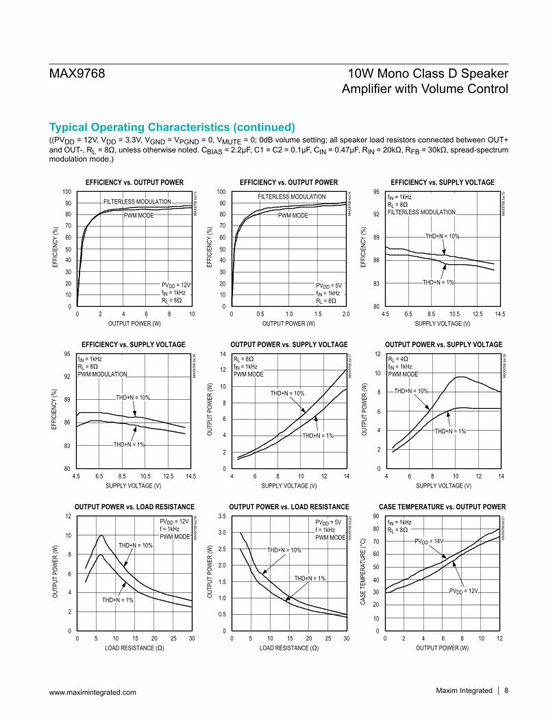
((PVDD = 12V, VDD = 3.3V, VGND = VPGND = 0, VMUTE = 0; 0dB volume setting; all speaker load resistors connected between OUT+ and OUT-, RL = 8Ω, unless otherwise noted. CBIAS = 2.2μF, C1 = C2 = 0.1μF, CIN = 0.47μF, RIN = 20kΩ, RFB = 30kΩ, spread-spectrum modulation mode.)
EFFICIENCY vs. OUTPUT POWERM
AX97
68 to
c13
OUTPUT POWER (W)
EFFI
CIEN
CY (%
)
104 6 82
20
10
30
5040
60
100
80
70
90
00
PWM MODE
PVDD = 12VfIN = 1kHzRL = 8Ω
FILTERLESS MODULATION
EFFICIENCY vs. OUTPUT POWER
MAX
9768
toc1
4
OUTPUT POWER (W)
EFFI
CIEN
CY (%
)
2.01.0 1.50.5
20
10
30
5040
60
100
80
70
90
00
PWM MODE
FILTERLESS MODULATION
PVDD = 5VfIN = 1kHzRL = 8Ω
EFFICIENCY vs. SUPPLY VOLTAGE
MAX
9768
toc1
5
SUPPLY VOLTAGE (V)
EFFI
CIEN
CY (%
)
14.58.5 10.5 12.56.5
83
86
89
95
92
804.5
THD+N = 10%
THD+N = 1%
fIN = 1kHzRL = 8ΩFILTERLESS MODULATION
EFFICIENCY vs. SUPPLY VOLTAGE
MAX
9768
toc1
6
SUPPLY VOLTAGE (V)
EFFI
CIEN
CY (%
)
14.58.5 10.5 12.56.5
83
86
89
95
92
804.5
fIN = 1kHzRL = 8ΩPWM MODULATION
THD+N = 10%
THD+N = 1%
OUTPUT POWER vs. SUPPLY VOLTAGEM
AX97
68 to
c17
SUPPLY VOLTAGE (V)
OUTP
UT P
OWER
(W)
148 10 126
2
4
6
8
14
12
10
04
RL = 8ΩfIN = 1kHzPWM MODE
THD+N = 10%
THD+N = 1%
OUTPUT POWER vs. SUPPLY VOLTAGE
MAX
9768
toc1
8
SUPPLY VOLTAGE (V)
OUTP
UT P
OWER
(W)
148 10 126
2
4
6
8
12
10
04
RL = 4ΩfIN = 1kHzPWM MODE
THD+N = 1%
THD+N = 10%
OUTPUT POWER vs. LOAD RESISTANCE
MAX
9768
toc1
9
LOAD RESISTANCE (Ω)
OUTP
UT P
OWER
(W)
3010 15 25205
2
4
6
8
12
10
00
PVDD = 12Vf = 1kHzPWM MODE
THD+N = 1%
THD+N = 10%
OUTPUT POWER vs. LOAD RESISTANCE
MAX
9768
toc2
0
LOAD RESISTANCE (Ω)
OUTP
UT P
OWER
(W)
3010 15 25205
0.5
1.0
1.5
2.5
2.0
3.5
3.0
00
PVDD = 5Vf = 1kHzPWM MODE
THD+N = 1%
THD+N = 10%
CASE TEMPERATURE vs. OUTPUT POWERM
AX97
68 to
c21
OUTPUT POWER (W)
CASE
TEM
PERA
TURE
(°C)
124 6 1082
10
30
20
40
50
70
60
90
80
00
fIN = 1kHzRL = 8Ω
PVDD = 14V
PVDD = 12V
MAX9768 10W Mono Class D Speaker Amplifier with Volume Control
Maxim Integrated 8www.maximintegrated.com
Typical Operating Characteristics (continued)

((PVDD = 12V, VDD = 3.3V, VGND = VPGND = 0, VMUTE = 0; 0dB volume setting; all speaker load resistors connected between OUT+ and OUT-, RL = 8Ω, unless otherwise noted. CBIAS = 2.2μF, C1 = C2 = 0.1μF, CIN = 0.47μF, RIN = 20kΩ, RFB = 30kΩ, spread-spectrum modulation mode.)
POWER-SUPPLY REJECTION RATIO (PVDD)vs. FREQUENCY
MAX
9768
toc2
2
FREQUENCY (Hz)
PSRR
(dB)
100k1k 10k100
-90
-70-80
-60
-50
-30
-40
0
-10
-20
-10010
PVDD = 12VVRIPPLE = 100mVP-PRL = 8Ω
PWM MODE
FILTERLESS MODULATION
POWER-SUPPLY REJECTION RATIO (VDD)vs. FREQUENCY
MAX
9768
toc2
3
FREQUENCY (Hz)
PSRR
(dB)
100k1k 10k100
-90
-70-80
-60
-50
-30
-40
0
-10
-20
-10010
VDD = 3.3VVRIPPLE = 100mVP-PRL = 8Ω
PWM MODE
FILTERLESS MODULATION
OUTPUT WAVEFORM(FILTERLESS MODULATION)
MAX9768 toc24
1µs/div
5V/div
5V/div
OUTPUT WAVEFORM (PWM MODE)MAX9768 toc25
1µs/div
5V/div
5V/div
OUTPUT FREQUENCY SPECTRUMM
AX97
68 to
c26
FREQUENCY (kHz)20105 15
-120
-100
-80
-40
-60
0
-20
-1400
FFM MODEVIN = -60dBVf = 1kHzRL = 8ΩUNWEIGHTED
OUTP
UT M
AGNI
TUDE
(dBV
)
OUTPUT FREQUENCY SPECTRUM
MAX
9768
toc2
7
FREQUENCY (kHz)20105 15
-120
-100
-80
-40
-60
0
-20
-1400
VIN = -60dBVf = 1kHzRL = 8ΩUNWEIGHTED
OUTP
UT M
AGNI
TUDE
(dBV
)
WIDEBAND OUTPUT SPECTRUM(FIXED-FREQUENCY MODULATION MODE)
MAX
9768
toc2
8
FREQUENCY (MHz)100010 100
-90
-100
-80
-70
-30
-40
-50-60
0
-10
-20
1
RBW = 10kHzINPUT AC GROUNDEDFILTERLESS MODULATION
OUTP
UT A
MPLIT
UDE
(dBV
)
WIDEBAND OUTPUT SPECTRUM(FIXED-FREQUENCY MODULATION MODE)
MAX
9768
toc2
9
FREQUENCY (MHz)100010 100
-90
-100
-80
-70
-30
-40
-50-60
0
-10
-20
1
RBW = 10kHzINPUT AC GROUNDEDPWM MODE
OUTP
UT A
MPLIT
UDE
(dBV
)
WIDEBAND OUTPUT SPECTRUM(SPREAD-SPECTRUM MODULATION MODE)
MAX
9768
toc3
0
FREQUENCY (MHz)100010 100
-90
-100
-80
-70
-30
-40
-50-60
0
-10
-20
1
OUTP
UT A
MPLIT
UDE
(dBV
)
RBW = 10kHzINPUT AC GROUNDEDFILTERLESS MODULATION
MAX9768 10W Mono Class D Speaker Amplifier with Volume Control
Maxim Integrated 9www.maximintegrated.com
Typical Operating Characteristics (continued)
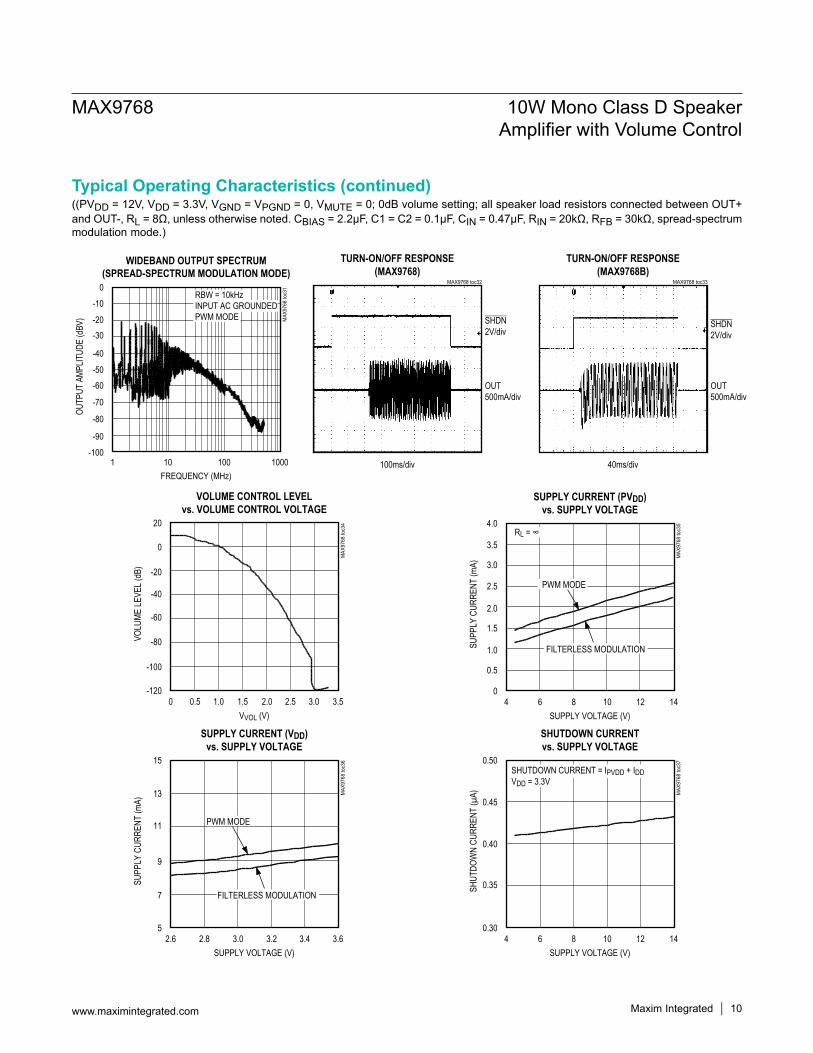
((PVDD = 12V, VDD = 3.3V, VGND = VPGND = 0, VMUTE = 0; 0dB volume setting; all speaker load resistors connected between OUT+ and OUT-, RL = 8Ω, unless otherwise noted. CBIAS = 2.2μF, C1 = C2 = 0.1μF, CIN = 0.47μF, RIN = 20kΩ, RFB = 30kΩ, spread-spectrum modulation mode.)
WIDEBAND OUTPUT SPECTRUM(SPREAD-SPECTRUM MODULATION MODE)
MAX
9768
toc3
1
FREQUENCY (MHz)100010 100
-90
-100
-80
-70
-30
-40
-50-60
0
-10
-20
1
OUTP
UT A
MPLIT
UDE
(dBV
)
RBW = 10kHzINPUT AC GROUNDEDPWM MODE
TURN-ON/OFF RESPONSE(MAX9768)
MAX9768 toc32
100ms/div
SHDN2V/div
OUT500mA/div
TURN-ON/OFF RESPONSE(MAX9768B)
MAX9768 toc33
40ms/div
SHDN2V/div
OUT500mA/div
VOLUME CONTROL LEVELvs. VOLUME CONTROL VOLTAGE
MAX
9768
toc3
4
VVOL (V)3.52.01.51.00.5 3.02.5
-100
-80
-60
-20
-40
20
0
-1200
VOLU
ME LE
VEL (
dB)
SUPPLY CURRENT (PVDD)vs. SUPPLY VOLTAGE
MAX
9768
toc3
5
SUPPLY VOLTAGE (V)141086 12
0.5
1.0
1.5
3.0
2.0
2.5
4.0
3.5
04
SUPP
LY C
URRE
NT (m
A)
PWM MODE
RL = ∞
FILTERLESS MODULATION
SUPPLY CURRENT (VDD)vs. SUPPLY VOLTAGE
MAX
9768
toc3
6
SUPPLY VOLTAGE (V)3.63.23.02.8 3.4
7
9
13
11
15
52.6
SUPP
LY C
URRE
NT (m
A)
PWM MODE
FILTERLESS MODULATION
SHUTDOWN CURRENTvs. SUPPLY VOLTAGE
MAX
9768
toc3
7
SUPPLY VOLTAGE (V)141086 12
0.35
0.45
0.40
0.50
0.304
SHUT
DOW
N CU
RREN
T (µ
A)
SHUTDOWN CURRENT = IPVDD + IDDVDD = 3.3V
MAX9768 10W Mono Class D Speaker Amplifier with Volume Control
Maxim Integrated 10www.maximintegrated.com
Typical Operating Characteristics (continued)

PIN NAME FUNCTION1, 2 OUT+ Positive Speaker Output
3, 16 PVDD Speaker Amplifier Power-Supply Input. Bypass with a 1µF capacitor to ground.
4 BOOT+ Positive Speaker Output Boost Flying-Capacitor Connection. Connect a 0.1µF ceramic capacitor between BOOT+ and OUT+.
5 SCLKI2C Serial-Clock Input and Modulation Scheme Select. In I2C mode (ADDR1 and ADDR2 ≠ GND) acts as I2C serial-clock input. Connect SCLK to VDD for classic PWM modulation, or connect SCLK to ground for filterless modulation.
6 SDA/VOL I2C Serial Data I/O and Analog Volume Control Input
7 FB Feedback. Connect feedback resistor between FB and IN to set amplifier gain. See the Adjustable Gain section.
8 IN Audio Input9, 11 GND Ground10 BIAS Common-Mode Bias Voltage. Bypass with a 2.2µF capacitor to GND.
12 SYNC
Frequency Select and External Clock Input.SYNC = GND: Fixed-frequency mode with fS = 300kHz.SYNC = Unconnected: Fixed-frequency mode with fS = 360kHz.SYNC = VDD: Spread-spectrum mode with fS = 300kHz ±7.5kHz.SYNC = Clocked: Fixed-frequency mode with fS = external clock frequency.
23+
24
22
21
8
7
9OU
T+
BOOT
+
SCLK
SDA/
VOL
10OU
T+
OUT-
BOOT
-
V DD
OUT-
SYNC
OUT
1 2
PGND
4 5 6
1718 16 14 13
ADDR2
ADDR1
BIAS
GND
IN
FB
MAX9768
PVDD
PVDD
3
15
PGND
20 11 GNDMUTE
19 12 SYNCSHDN
TQFN(4mm x 4mm)
TOP VIEW
MAX9768 10W Mono Class D Speaker Amplifier with Volume Control
www.maximintegrated.com Maxim Integrated 11
Pin Description
Pin Configuration
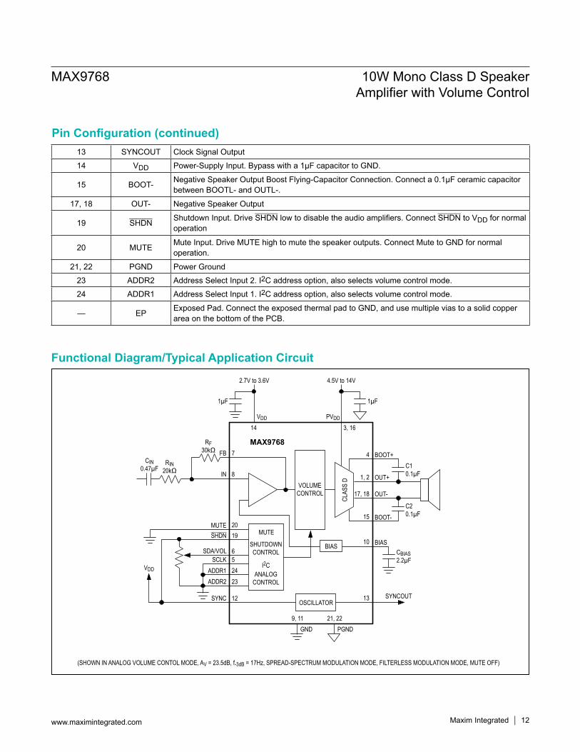
13 SYNCOUT Clock Signal Output14 VDD Power-Supply Input. Bypass with a 1µF capacitor to GND.
15 BOOT- Negative Speaker Output Boost Flying-Capacitor Connection. Connect a 0.1µF ceramic capacitor between BOOTL- and OUTL-.
17, 18 OUT- Negative Speaker Output
19 SHDN Shutdown Input. Drive SHDN low to disable the audio amplifiers. Connect SHDN to VDD for normal operation
20 MUTE Mute Input. Drive MUTE high to mute the speaker outputs. Connect Mute to GND for normal operation.
21, 22 PGND Power Ground23 ADDR2 Address Select Input 2. I2C address option, also selects volume control mode.24 ADDR1 Address Select Input 1. I2C address option, also selects volume control mode.
— EP Exposed Pad. Connect the exposed thermal pad to GND, and use multiple vias to a solid copper area on the bottom of the PCB.
MUTE
VOLUMECONTROL
CLAS
S D
SHUTDOWNCONTROL
OSCILLATORSYNCOUT
BIAS
14VDD
VDD
PVDD
CBIAS2.2µF
7
8 1, 2
4
17, 18
15
10
13
FBRF
30kΩ
RIN20kΩ
CIN0.47µF C1
0.1µF
C20.1µF
1µF1µF
IN
2019
652423
GND PGND
OUT+
BOOT+
OUT-
BOOT-
BIAS
12
3, 16
9, 11 21, 22
2.7V to 3.6V 4.5V to 14V
SYNC
MUTESHDN
SDA/VOLSCLK
ADDR1ADDR2
I2CANALOG
CONTROL
MAX9768
(SHOWN IN ANALOG VOLUME CONTOL MODE, AV = 23.5dB, f-3dB = 17Hz, SPREAD-SPECTRUM MODULATION MODE, FILTERLESS MODULATION MODE, MUTE OFF)
MAX9768 10W Mono Class D Speaker Amplifier with Volume Control
www.maximintegrated.com Maxim Integrated 12
Functional Diagram/Typical Application Circuit
Pin Configuration (continued)
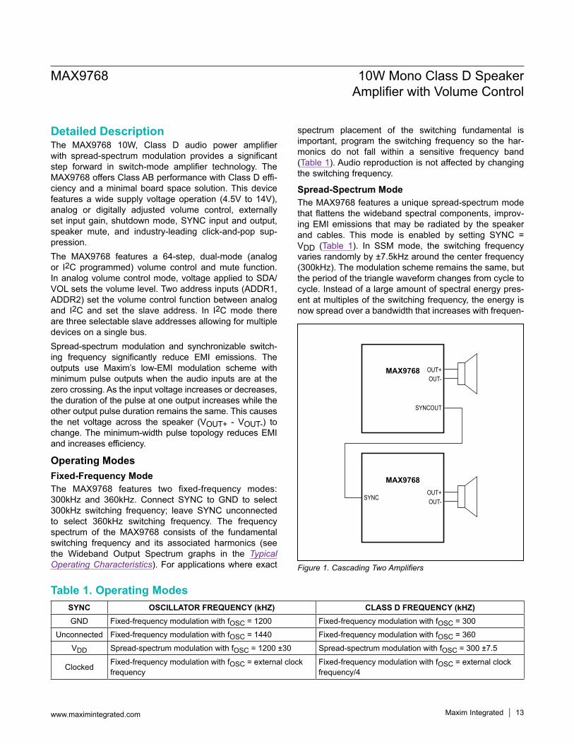
Detailed DescriptionThe MAX9768 10W, Class D audio power amplifier with spread-spectrum modulation provides a significant step forward in switch-mode amplifier technology. The MAX9768 offers Class AB performance with Class D effi-ciency and a minimal board space solution. This device features a wide supply voltage operation (4.5V to 14V), analog or digitally adjusted volume control, externally set input gain, shutdown mode, SYNC input and output, speaker mute, and industry-leading click-and-pop sup-pression.The MAX9768 features a 64-step, dual-mode (analog or I2C programmed) volume control and mute function. In analog volume control mode, voltage applied to SDA/VOL sets the volume level. Two address inputs (ADDR1, ADDR2) set the volume control function between analog and I2C and set the slave address. In I2C mode there are three selectable slave addresses allowing for multiple devices on a single bus.Spread-spectrum modulation and synchronizable switch-ing frequency significantly reduce EMI emissions. The outputs use Maxim’s low-EMI modulation scheme with minimum pulse outputs when the audio inputs are at the zero crossing. As the input voltage increases or decreases, the duration of the pulse at one output increases while the other output pulse duration remains the same. This causes the net voltage across the speaker (VOUT+ - VOUT-) to change. The minimum-width pulse topology reduces EMI and increases efficiency.
Operating ModesFixed-Frequency ModeThe MAX9768 features two fixed-frequency modes: 300kHz and 360kHz. Connect SYNC to GND to select 300kHz switching frequency; leave SYNC unconnected to select 360kHz switching frequency. The frequency spectrum of the MAX9768 consists of the fundamental switching frequency and its associated harmonics (see the Wideband Output Spectrum graphs in the Typical Operating Characteristics). For applications where exact
spectrum placement of the switching fundamental is important, program the switching frequency so the har-monics do not fall within a sensitive frequency band (Table 1). Audio reproduction is not affected by changing the switching frequency.
Spread-Spectrum ModeThe MAX9768 features a unique spread-spectrum mode that flattens the wideband spectral components, improv-ing EMI emissions that may be radiated by the speaker and cables. This mode is enabled by setting SYNC = VDD (Table 1). In SSM mode, the switching frequency varies randomly by ±7.5kHz around the center frequency (300kHz). The modulation scheme remains the same, but the period of the triangle waveform changes from cycle to cycle. Instead of a large amount of spectral energy pres-ent at multiples of the switching frequency, the energy is now spread over a bandwidth that increases with frequen-
Figure 1. Cascading Two Amplifiers
Table 1. Operating ModesSYNC OSCILLATOR FREQUENCY (kHZ) CLASS D FREQUENCY (kHZ)GND Fixed-frequency modulation with fOSC = 1200 Fixed-frequency modulation with fOSC = 300
Unconnected Fixed-frequency modulation with fOSC = 1440 Fixed-frequency modulation with fOSC = 360VDD Spread-spectrum modulation with fOSC = 1200 ±30 Spread-spectrum modulation with fOSC = 300 ±7.5
Clocked Fixed-frequency modulation with fOSC = external clock frequency
Fixed-frequency modulation with fOSC = external clock frequency/4
SYNCOUT
OUT+OUT-
OUT+OUT-SYNC
MAX9768
MAX9768
MAX9768 10W Mono Class D Speaker Amplifier with Volume Control
www.maximintegrated.com Maxim Integrated 13

cy. Above a few megahertz, the wideband spectrum looks like white noise for EMI purposes. A proprietary amplifier topology ensures this does not corrupt the noise floor in the audio bandwidth.
External Clock ModeThe SYNC input allows the MAX9768 to be synchronized to an external clock, or another Maxim Class D ampli-fier, creating a fully synchronous system, minimizing clock intermodulation, and allocating spectral components of the switching harmonics to insensitive frequency bands. Applying a clock signal between 1MHz and 1.6MHz to SYNC synchronizes the MAX9768. The Class D switching frequency is equal to one-fourth the SYNC input frequency.SYNCOUT is equal to the SYNC input frequency and allows several Maxim amplifiers to be cascaded. The synchronized output minimizes interference due to clock intermodulation caused by the switching spread between single devices. The modulation scheme remains the same when using SYNCOUT, and audio reproduction is not affected (Figure 1). Current flowing between SYNCOUT of a master device and SYNC of a slave device is low as the SYNC input is high impedance (typically 200kΩ).
Filterless Modulation/PWM ModulationThe MAX9768 features two output modulation schemes: filterless modulation or classic PWM, selectable through SCLK when the device is in analog mode (ADDR2 and ADDR1 = GND, Table 2) or through the I2C interface (Table 7). Maxim’s unique, filterless modulation scheme eliminates the LC filter required by traditional Class D amplifiers, reducing component count, conserving board space and system cost. Although the MAX9768 meets FCC and other EMI limits with a low-cost ferrite bead filter, many applications still may want to use a full LC-filtered output. If using a full LC filter, the performance is best with the MAX9768 configured for classic PWM output.Switching between schemes while in normal operating mode with the I2C interface, the output is not click-and-pop protected. To have click-and-pop protection when switching between output schemes, the device must enter shutdown mode and be configured to the new output scheme before the startup sequence is terminated.The startup time for the MAX9768 is typically 220ms. The startup time for the MAX9768B is typically 15ms.
EfficiencyEfficiency of a Class D amplifier is due to the switching operation of the output stage transistors. In a Class D amplifier, the output transistors act as current-steering switches and consume negligible additional power. Any power loss associated with the Class D output stage is mostly due to the I2R loss of the MOSFET on-resistance, and quiescent-current overhead.The theoretical best efficiency of a linear amplifier is 78%, however, that efficiency is only exhibited at peak output power. Under normal operating levels (typical music reproduction levels), efficiency falls below 30%, whereas the MAX9768 still exhibits > 80% efficiencies under the same conditions (Figure 2).
Soft Current LimitWhen the output current exceeds the soft current limit, 2A (typ), the MAX9768 enters a cycle-by-cycle current-limit mode. In soft current-limit mode, the output is clipped at 2A. When the output decreases so the output current falls below 2A, normal operation resumes. The effect of soft current limiting is a slight increase in distortion. Most
Table 2. Modulation Scheme Selection In Analog Mode
Figure 2. MAX9768 Efficiency vs. Class AB Efficiency
ADDR2 ADDR1 SDA/VOL SCLK FUNCTION0 0 Analog Volume Control 0 Filterless Modulation0 0 Analog Volume Control 1 Classic PWM (50% Duty Cycle)
EFFICIENCY vs. OUTPUT POWER
MAX9
768 f
ig02
OUTPUT POWER (W)
EFFI
CIEN
CY (%
)
8642
10
20
30
40
50
60
70
80
90
100
00 10
MAX9768
CLASS AB
PVDD = 12VfIN = 1kHzRL = 8Ω
MAX9768 10W Mono Class D Speaker Amplifier with Volume Control
www.maximintegrated.com Maxim Integrated 14

applications will not enter soft current-limit mode unless the speaker or filter creates impedance nulls below 8Ω.
Hard Current LimitWhen the output current exceeds the hard current limit, 2.5A (typ), the MAX9768 disables the outputs and initiates a startup sequence. This startup sequence takes 220ms for the MAX9768 and 15ms for the MAX9768B. The shut-down and startup sequence is repeated until the output fault is removed. When in hard current limit, the output may make a soft clicking sound. The average supply current is relatively low, as the duty cycle of the output short is brief. Most applications will not enter hard current-limit mode unless the output is short circuited or incorrectly connected.
Thermal ShutdownWhen the die temperature exceeds the thermal shutdown threshold, +150°C (typ), the MAX9768 outputs are dis-abled. When the die temperature decreases below +135°C (typ), normal operation resumes. The effect of thermal shut-down is an output signal turning off for approximately 3s in most applications, depending on the thermal time constant of the audio system. Most applications should never enter thermal shutdown. Some of the possible causes of thermal shutdown are too low of a load impedance, high ambient temperature, poor PCB layout and assembly, or excessive output overdrive.
ShutdownThe MAX9768 features a shutdown mode that reduces power consumption and extends battery life. Driving SHDN low places the device in low-power (0.5μA) shutdown mode. Connect SHDN to digital high for normal opera-tion. In shutdown mode, the outputs are high impedance, SYNCOUT is pulled high, the BIAS voltage decays to zero, and the common-mode input voltage decays to zero. The I2C register retains its contents during shutdown.
Undervoltage Lockout (UVLO)The MAX9768 features an undervoltage lockout protection that shuts down the device if either of the supplies are too low. The device will go into shutdown if VDD is less than 2.5V (VDD UVLO = 2.5V) or if PVDD is less than 4V (PVDD UVLO = 4V).
Mute FunctionThe MAX9768 features a clickless/popless mute mode. When the device is muted, the outputs do not stop switching, only the volume level is muted to the speaker. To mute the MAX9768, drive MUTE to logic-high. MUTE should be held high during system power-up and power-down to ensure optimum click-and-pop performance.
Volume ControlThe volume control operates from either an analog volt-age input or through the I2C interface. The volume control has 64 levels, with the lowest setting equal to mute.To set the device to analog mode, connect ADDR1 and ADDR2 to GND. In analog mode, SDA/VOL is an analog input for volume control, see the Functional Diagram/Typical Application Circuit. The analog input range is ratiometric between 0.9 x VDD and 0.1 x VDD, where 0.9 x VDD = full mute and 0.1 x VDD = full volume (Table 6).In I2C mode, volume control for the speaker is controlled separately by the command register (see Table 4, Table 5, and Table 6). See the Write Data Format section for more information regarding formatting data and tables to set volume levels.
I2C InterfaceThe MAX9768 features an I2C 2-wire serial interface con-sisting of a serial data line (SDA) and a serial clock line (SCL). SDA and SCL facilitate communication between the MAX9768 and the master at clock rates up to 400kHz. When the MAX9768 is used on an I2C bus with multiple devices, the VDD supply must stay powered on to ensure proper I2C bus operation. The master, typically a micro-controller, generates SCL and initiates data transfer on the bus. Figure 3 shows the 2-wire interface timing diagram.A master device communicates to the MAX9768 by trans-mitting the proper address followed by the data word. Each transmit sequence is framed by a START (S) or REPEATED START (Sr) condition and a STOP (P) condi-tion. Each word transmitted over the bus is 8 bits long and is always followed by an acknowledge clock pulse.The MAX9768 SDA line operates as both an input and an open-drain output. A pullup resistor, greater than 500Ω, is required on the SDA bus. The MAX9768 SCL line oper-ates as an input only. A pullup resistor, greater than 500Ω, is required on SCL if there are multiple masters on the bus, or if the master in a single-master system has an open-drain SCL output. Series resistors in line with SDA and SCL are optional. The SCL and SDA inputs suppress noise spikes to assure proper device operation even on a noisy bus.
Bit TransferOne data bit is transferred during each SCL cycle. The data on SDA must remain stable during the high period of the SCL pulse. Changes in SDA while SCL is high are control signals (see the START and STOP Conditions section). SDA and SCL idle high when the I2C bus is not busy.
MAX9768 10W Mono Class D Speaker Amplifier with Volume Control
www.maximintegrated.com Maxim Integrated 15

START and STOP ConditionsA master device initiates communication by issuing a START condition. A START condition is a high-to-low transition on SDA with SCL high. A STOP condition is a low-to-high transition on SDA while SCL is high (Figure 4). A START (S) condition from the master signals the beginning of a transmission to the MAX9768. The master terminates transmission, and frees the bus, by issuing a STOP (P) condition. The bus remains active if a REPEATED START (Sr) condition is generated instead of a STOP condition.
Early STOP ConditionsThe MAX9768 recognizes a STOP condition at any point during data transmission except if the STOP condition occurs in the same high pulse as a START condition.
Slave AddressThe slave address of the MAX9768 is 8 bits and consist-
ing of 3 fields: the first field is 5 bits wide and is fixed
(10010). The second is a 2-bit field, which is set through ADDR2 and ADDR1 (externally connected as logic-high or low). Third field is a R/W flag bit. Set R/W = 0 to write to the slave. A representation of the slave address is shown in Table 3.When ADDR1 and ADDR2 are connected to GND, serial interface communication is disabled. Table 4 summarizes the slave address of the device as a function of ADDR1 and ADDR2.
AcknowledgeThe acknowledge bit (ACK) is a clocked 9th bit that the MAX9768 uses to handshake receipt each byte of data (Figure 5). The MAX9768 pulls down SDA during the mas-ter-generated 9th clock pulse. The SDA line must remain stable and low during the high period of the acknowledge clock pulse. Monitoring ACK allows for detection of unsuc-cessful data transfers. An unsuccessful data transfer occurs if a receiving device is busy or if a system fault has occurred. In the event of an unsuccessful data transfer, the bus master can reattempt communication.
Write Data FormatA write to the MAX9768 includes transmission of a START condition, the slave address with the R/W bit set to 0 (see Table 3), one byte of data to the command register, and a STOP condition. Figure 6 illustrates the proper format for one frame.
Figure 3. 2-Wire Serial-Interface Timing Diagram
Figure 4. START, STOP, and REPEATED START Conditions
SCL
SDA
STARTCONDITION
STOPCONDITION
REPEATED START
CONDITION
START CONDITION
tHD,STA
tSU,STAtHD,STA tSP
tBUF
tSU,STOtLOW
tSU,DAT
tHD,DAT
tHIGH
tR tF
SCL
SDA
S Sr P
MAX9768 10W Mono Class D Speaker Amplifier with Volume Control
www.maximintegrated.com Maxim Integrated 16

Volume ControlThe command register is used to control the volume level of the speaker amplifier. The two MSBs (D7 and D6) should be set to 00 to choose the speaker register. V5–V0 is the volume control data that will be written into the addresses register to set the volume level (see Table 5 and Table 6).For a write byte operation, the master sends a single byte to the slave device (MAX9768). This is done as follows:1) The master sends a start condition.2) The master sends the 7-bit slave ID plus a write bit
(low).3) The addressed slave asserts an ACK on the data
line.4) The master sends 8 data bits.5) The active slave asserts an ACK (or NACK) on the
data line.6) The master generates a stop condition.
Applications InformationFilterless Class D OperationThe MAX9768 can be operated without a filter and meet common EMC radiation limits when the speaker leads are less than approximately 10cm. Lengths beyond 10cm are possible but should be verified against the appropriate EMC standard. Select the filter-less modulation mode with spread-spectrum modulation mode for best performance.For longer speaker wire lengths, a simple ferrite bead and capacitor-based filter can be used to meet EMC limits. See Figure 7 for the correct connections of these com-ponents. Select a ferrite bead with 100Ω to 600Ω imped-ance, and rated for at least 1.5A. The capacitor value will vary based on the ferrite bead chosen and the actual
Figure 5. Acknowledge
Figure 6. Write Data Format Example
Table 3. Slave Address Block
Table 4. Slave Address Table 5. Data Byte Format
SA7 (MSB) SA6 SA5 SA4 SA3 SA2 SA1 SA0 (LSB)1 0 0 1 0 ADDR2 ADDR1 R/W
ADDR2 ADDR1 SLAVE ADDRESS0 0 Disabled0 1 1001001_1 0 1001010_1 1 1001011_
D7(MSB) D6 D5 D4 D3 D2 D1 D0
(LSB)0 0 V5 V4 V3 V2 V1 V0
1SCL
STARTCONDITION
SDA
2 8 9
CLOCK PULSE FORACKNOWLEDGMENT
ACKNOWLEDGE
NOT ACKNOWLEDGE
S SLAVE ADDRESS
7 bits
WRITE BYTE FORMAT
WR ACK DATA
8 bits
ACK P
DATA BYTE: GIVES A COMMAND.SLAVE ADDRESS:EQUIVALENT TO CHIP-SELECT LINE OF A 3-WIRE INTERFACE.
0
MAX9768 10W Mono Class D Speaker Amplifier with Volume Control
www.maximintegrated.com Maxim Integrated 17

Table 6. Speaker Volume Levels
V5 V4 V3 V2 V1 V0 VOLUME POSITION
VOLUME LEVEL (dB)
STEP SIZE(dB)
1 1 1 1 1 1 63 9.5 0.71 1 1 1 1 0 62 8.8 0.71 1 1 1 0 1 61 8.2 0.61 1 1 1 0 0 60 7.6 0.61 1 1 0 1 1 59 7.0 0.61 1 1 0 1 0 58 6.5 0.51 1 1 0 0 1 57 5.9 0.51 1 1 0 0 0 56 5.4 0.51 1 0 1 1 1 55 4.9 0.51 1 0 1 1 0 54 4.4 0.51 1 0 1 0 1 53 3.9 0.61 1 0 1 0 0 52 3.4 0.41 1 0 0 1 1 51 2.9 0.51 1 0 0 1 0 50 2.4 0.41 1 0 0 0 1 49 2.0 0.41 1 0 0 0 0 48 1.6 0.41 0 1 1 1 1 47 1.2 0.71 0 1 1 1 0 46 0.5 1.01 0 1 1 0 1 45 -0.5 1.51 0 1 1 0 0 44 -1.9 1.51 0 1 0 1 1 43 -3.4 1.51 0 1 0 1 0 42 -5.0 1.11 0 1 0 0 1 41 -6.0 1.11 0 1 0 0 0 40 -7.1 1.81 0 0 1 1 1 39 -8.9 1.01 0 0 1 1 0 38 -9.9 1.01 0 0 1 0 1 37 -10.9 1.11 0 0 1 0 0 36 -12.0 1.21 0 0 0 1 1 35 -13.1 1.31 0 0 0 1 0 34 -14.4 0.91 0 0 0 0 1 33 -15.4 1.01 0 0 0 0 0 32 -16.4 1.1
MAX9768 10W Mono Class D Speaker Amplifier with Volume Control
www.maximintegrated.com Maxim Integrated 18

Table 6. Speaker Volume Levels (continued)
V5 V4 V3 V2 V1 V0 VOLUME POSITION
VOLUME LEVEL (dB)
STEP SIZE(dB)
0 1 1 1 1 1 31 -17.5 2.20 1 1 1 1 0 30 -19.7 1.90 1 1 1 0 1 29 -21.6 1.90 1 1 1 0 0 28 -23.5 1.70 1 1 0 1 1 27 -25.2 2.00 1 1 0 1 0 26 -27.2 2.60 1 1 0 0 1 25 -29.8 1.60 1 1 0 0 0 24 -31.5 2.00 1 0 1 1 1 23 -33.4 2.50 1 0 1 1 0 22 -36.0 1.60 1 0 1 0 1 21 -37.6 2.00 1 0 1 0 0 20 -39.6 2.50 1 0 0 1 1 19 -42.1 1.60 1 0 0 1 0 18 -43.7 2.00 1 0 0 0 1 17 -45.6 2.50 1 0 0 0 0 16 -48.1 2.50 0 1 1 1 1 15 -50.6 3.50 0 1 1 1 0 14 -54.2 2.50 0 1 1 0 1 13 -56.7 3.50 0 1 1 0 0 12 -60.2 2.50 0 1 0 1 1 11 -62.7 3.50 0 1 0 1 0 10 -66.2 2.50 0 1 0 0 1 9 -68.7 3.50 0 1 0 0 0 8 -72.2 2.50 0 0 1 1 1 7 -74.7 3.50 0 0 1 1 0 6 -78.3 2.50 0 0 1 0 1 5 -80.8 3.50 0 0 1 0 0 4 -84.3 2.50 0 0 0 1 1 3 -86.8 3.50 0 0 0 1 0 2 -90.3 2.50 0 0 0 0 1 1 -92.8 —0 0 0 0 0 0 0 (MUTE) -161.5 —
MAX9768 10W Mono Class D Speaker Amplifier with Volume Control
www.maximintegrated.com Maxim Integrated 19

speaker lead length. Select the capacitor value based on EMC performance.When doing bench evaluation without a filter or a ferrite bead filter, include a series inductor (68μH for 8Ω load) to model the actual loudspeaker’s behavior. If this inductance is omitted, the MAX9768 will have reduced efficiency and output power, as well as worse THD+N performance.
Inductor-Based Output FiltersSome applications will use the MAX9768 with a full induc-tor-/capacitor-based (LC) output filter. This is common for longer speaker lead lengths, and to gain increased margin to EMC limits. Select the PWM output mode and use fixed-frequency modulation mode for best audio performance. See Figure 8 for the correct connections of these components.The component selection is based on the load impedance of the speaker. Table 8 lists suggested values for a variety of load impedances.Inductors L3 and L4, and capacitor C15 form the primary output filter. In addition to these primary filter components, other components in the filter improve its functionality. Capacitors C13 and C14, plus resistors R6 and R7, form a Zobel at the output. A Zobel corrects the output load-
ing to compensate for the rising impedance of the loud-speaker. Without a Zobel, the filter will have a peak in its response near the cutoff frequency. Capacitors C11 and C12 provide additional high-frequency bypass to reduce radiated emissions.
Adjustable GainGain-Setting ResistorsExternal feedback resistors set the gain of the MAX9768. The output stage has an internal 20dB gain in addition to the externally set gain. Set the maximum gain by using resistors RF and RIN (Figure 9) as follows:
FV
IN
RA 10 V / VR = −
Choose RF between 10kΩ and 50kΩ. Please note that the actual gain of the amplifier is dependent on the volume level setting. For example, with the volume control set to +9.5dB, the amplifier gain would be 9.5dB + 20dB, assum-ing RF = RIN.The input amplifier can be configured into a variety of circuits. The FB terminal is an actual operational ampli-fier output, allowing the MAX9768 to be configured as a summing amplifier, a filter, or an equalizer, for example.
Table 7. Setting Class D Output Modulation Scheme
*Power-on default.
Figure 7. Ferrite Bead Filter
D7 (MSB) D6 D5 D4 D3 D2 D1 D0 (LSB) FUNCTION1 1 0 1 0 1 0 1 Classic PWM1 1 0 1 0 1 1 0 FILTERLESS MODULATION*
BOOT_+
C10.1µF
C9330pF
C10330pF
OUT_+
BOOT_-
C20.1µF
OUT_-
MAX9768
MAX9768 10W Mono Class D Speaker Amplifier with Volume Control
www.maximintegrated.com Maxim Integrated 20

Power SuppliesThe MAX9768 has different supplies for each portion of the device, allowing for the optimum combination of head-room power dissipation and noise immunity. The speaker amplifiers are powered from PVDD and can range from 4.5V to 14V. The remainder of the device is powered by VDD. Power supplies are independent of each other so sequencing is not necessary. Power may be supplied by separate sources or derived from a single higher source using a linear regulator to reduce the voltage, as shown in Figure 10.
Component SelectionInput FilterAn input capacitor, CIN, in conjunction with the input resis-tor of the MAX9768 forms a highpass filter that removes the DC bias from an incoming signal. The AC-coupling capacitor allows the amplifier to automatically bias the signal to an optimum DC level. Assuming zero source impedance, the -3dB point of the highpass filter is given by:
f 3dBIN IN
1 2 R C− =π
Choose CIN so f-3dB is well below the lowest frequency of interest. Use capacitors whose dielectrics have lowvoltage coefficients, such as tantalum or aluminum electrolytic. Capacitors with high-voltage coefficients, such as ceram-ics, may result in increased distortion at low frequencies.Other considerations when designing the input filter include the constraints of the overall system and the actual frequency band of interest. Although high-fidelity audio calls for a flat-gain response between 20Hz and 20kHz, portable voice-reproduction devices such as cellu-lar phones and two-way radios need only concentrate on the frequency range of the spoken human voice (typically 300Hz to 3.5kHz). In addition, speakers used in portable devices typically have a poor response below 300Hz. Taking these two factors into consideration, the input filter may not need to be designed for a 20Hz to 20kHz response, saving both board space and cost due to the use of smaller capacitors.
BIAS CapacitorBIAS is the output of the internally generated DC bias voltage. The BIAS bypass capacitor, CBIAS, improves PSRR and THD+N by reducing power supply and other noise sources at the common-mode bias node. Bypass BIAS with a 2.2μF capacitor to GND.
Table 8. Suggested Values for LC filter
Figure 8. Output Filter for PWM Mode
RL (Ω) L3, L4 (µH) C15 (µF) C11, C12 (µF) R6, R7 (Ω) C13, C14 (µF)6 15 0.33 0.01 7.5 0.688 22 0.22 0.01 10 0.47
12 33 0.1 0.01 15 0.33
BOOT_+C10.1µF
OUT_+ L4
4
1, 2
C11C15
R6
MAX9768C13
L314, 18
15BOOT_-
C20.1µF
OUT_-
C12 R7
RL
C14
MAX9768 10W Mono Class D Speaker Amplifier with Volume Control
www.maximintegrated.com Maxim Integrated 21

Supply Bypassing, Layout, and GroundingProper layout and grounding are essential for optimum performance. Use large traces for the power-supply inputs and amplifier outputs to minimize losses due to parasitic trace resistance. Large traces also aid in moving heat away from the package. Proper grounding improves audio performance, minimizes crosstalk between chan-nels, and prevents any switching noise from coupling into the audio signal. Connect PGND and GND together at a single point on the PCB. Route all traces that carry switch-ing transients away from GND and the traces/components in the audio signal path.
Bypass VDD and PVDD with a 1μF capacitor to PGND. Place the bypass capacitors as close to the MAX9768 as possible. Place a bulk capacitor between PVDD and PGND, if needed.Use large, low-resistance output traces. Current drawn from the outputs increase as load impedance decreases. High output trace resistance decreases the power deliv-ered to the load. Large output, supply, and GND traces allow more heat to move from the MAX9768 to the air, decreasing the thermal impedance of the circuit if possible.
Figure 9. Setting Gain Figure 10. Using a Linear Regulator to Produce 3.3V from a 12V Power Supply
BOOT+
OUT+
AUDIOINPUT MAX9768CIN
BOOT-
OUT-
IN
FB
RIN
RF
GNDGND
MAX9768SHDN OUT
3.3V VDD
PVDDIN1µF
MAX1726
12V
1µF
MAX9768 10W Mono Class D Speaker Amplifier with Volume Control
www.maximintegrated.com Maxim Integrated 22

Note: All devices are specified over the -40°C to +85°C operating temperature range.+Denotes a lead(Pb)-free/RoHS-compliant package. /V Denotes an automotive-qualified part, *EP = Exposed pad.
PART PIN-PACKAGE tON (ms)MAX9768ETG+ 24 TQFN-EP* 220MAX9768BETG+ 24 TQFN-EP* 15MAX9768BETG/V+ 24 TQFN-EP* 15
Ordering Information
MAX9768 10W Mono Class D Speaker Amplifier with Volume Control
www.maximintegrated.com Maxim Integrated 23
Chip InformationPROCESS: BiCMOS

PACKAGE TYPE PACKAGE CODE DOCUMENT NO.24 TQFN-EP T2444+4 21-0139
MAX9768 10W Mono Class D Speaker Amplifier with Volume Control
www.maximintegrated.com Maxim Integrated 24
Package InformationFor the latest package outline information and land patterns (footprints), go to www.maximintegrated.com/packages. Note that a “+”, “#”, or “-” in the package code indicates RoHS status only. Package drawings may show a different suffix character, but the drawing pertains to the package regardless of RoHS status.
REVISIONNUMBER
REVISIONDATE DESCRIPTION PAGES
CHANGED0 9/07 Initial release —1 3/08 Updated package outline 24, 252 11/08 Corrected various items 2, 4, 5, 11
3 12/17Converted data sheet to new template; updated globals in Electrical Characteristics and Typical Operating Characteristics, and added new variant (MAX9768BETG/V+) to Ordering Information
1‒25
Maxim Integrated cannot assume responsibility for use of any circuitry other than circuitry entirely embodied in a Maxim Integrated product. No circuit patent licenses are implied. Maxim Integrated reserves the right to change the circuitry and specifications without notice at any time. The parametric values (min and max limits) shown in the Electrical Characteristics table are guaranteed. Other parametric values quoted in this data sheet are provided for guidance.
Maxim Integrated and the Maxim Integrated logo are trademarks of Maxim Integrated Products, Inc.
MAX9768 10W Mono Class D Speaker Amplifier with Volume Control
© 2017 Maxim Integrated Products, Inc. 25
Revision History
For pricing, delivery, and ordering information, please contact Maxim Direct at 1-888-629-4642, or visit Maxim Integrated’s website at www.maximintegrated.com.