MAX4230–MAX4234 - Maxim Integrated · General Description The MAX4230–MAX4234 single/dual/quad,...
15
General Description The MAX4230–MAX4234 single/dual/quad, high-output drive CMOS op amps feature 200mA of peak output cur- rent, rail-to-rail input, and output capability from a single 2.7V to 5.5V supply. These amplifiers exhibit a high slew rate of 10V/μs and a gain-bandwidth product (GBWP) of 10MHz. The MAX4230–MAX4234 can drive typical headset levels (32Ω), as well as bias an RF power amplifier (PA) in wireless handset applications. The MAX4230 comes in a tiny 5-pin SC70 package and the MAX4231, single with shutdown, is offered in a 6-pin SC70 package and in 1.5mm x 1.0mm UCSP and thin μDFN packages. The dual op-amp MAX4233 is offered in the space-saving 10-bump chip-scale package (UCSP™), providing the smallest footprint area for a dual op amp with shutdown. These op amps are designed to be part of the PA control circuitry, biasing RF PAs in wireless headsets. The MAX4231/ MAX4233 offer a SHDN feature that drives the output low. This ensures that the RF PA is fully disabled when needed, preventing unconverted signals to the RF antenna. Applications ● RF PA Biasing Controls in Handset Applications ● Portable/Battery-Powered Audio Applications ● Portable Headphone Speaker Drivers (32Ω) ● Audio Hands-Free Car Phones (Kits) ● Tablet/Notebook Computers ● Digital-to-Analog Converter Buffers ● Transformer/Line Drivers ● Motor Drivers Benefits and Features ● Optimized for Headsets and High-Current Outputs • 200mA Output Drive Capability • 100dB Voltage Gain (R L = 100kΩ) • 85dB Power-Supply Rejection Ratio • No Phase Reversal for Overdriven Inputs • Unity-Gain Stable for Capacitive Loads to 780pF ● Suitable for High-Bandwidth Applications • 10MHz Gain-Bandwidth Product • High Slew Rate: 10V/μs ● Extends the Battery Life of Portable Applications • 1.1mA Supply Current per Amplifier ● Low-Power Shutdown Mode Reduces Supply Current to < 1μA ● Small Package Options • Tiny, 2.1mm x 2.0mm Space-Saving SC70 Package ● AEC-Q100 Qualified, Refer to Ordering Information for the List of /V Parts Selector Guide appears at end of data sheet. Pin/Bump Configurations appear at end of data sheet. Ordering Information continued at end of data sheet. Visit www.maximintegrated.com/products/patents for product patent marking information. UCSP is a trademark of Maxim Integrated Products, Inc. 19-2164; Rev 21; 2/18 +Denotes a lead(Pb)-free/RoHS-compliant package. T = Tape and reel. PART TEMP RANGE PIN- PACKAGE TOP MARK MAX4230AXK+T -40°C to +125°C 5 SC70 ACS MAX4230AXK/V+T -40°C to +125°C 5 SC70 +AUU MAX4230AUK+T -40°C to +125°C 5 SOT23 ABZZ MAX4231AXT+T -40°C to +125°C 6 SC70 ABA MAX4231AUT+T -40°C to +125°C 6 SOT23 ABNF MAX4231ART+T -40°C to +125°C 6 UCSP AAM MAX4231AYT+T -40°C to +125°C 6 Thin µDFN (Ultra-Thin LGA) +AH MAX4231 DAC SHDN C RF RISO CLOAD ILOAD = 30mA ANTENNA R PA 2.7V TO 5.5V MAX4230–MAX4234 High-Output-Drive, 10MHz, 10V/μs, Rail-to-Rail I/O Op Amps with Shutdown in SC70 Typical Operating Circuit Ordering Information
-
Upload
trinhduong -
Category
Documents
-
view
222 -
download
0
Transcript of MAX4230–MAX4234 - Maxim Integrated · General Description The MAX4230–MAX4234 single/dual/quad,...
General DescriptionThe MAX4230–MAX4234 single/dual/quad, high-output drive CMOS op amps feature 200mA of peak output cur-rent, rail-to-rail input, and output capability from a single 2.7V to 5.5V supply. These amplifiers exhibit a high slew rate of 10V/μs and a gain-bandwidth product (GBWP) of 10MHz. The MAX4230–MAX4234 can drive typical headset levels (32Ω), as well as bias an RF power amplifier (PA) in wireless handset applications. The MAX4230 comes in a tiny 5-pin SC70 package and the MAX4231, single with shutdown, is offered in a 6-pin SC70 package and in 1.5mm x 1.0mm UCSP and thin μDFN packages. The dual op-amp MAX4233 is offered in the space-saving 10-bump chip-scale package (UCSP™), providing the smallest footprint area for a dual op amp with shutdown.These op amps are designed to be part of the PA control circuitry, biasing RF PAs in wireless headsets. The MAX4231/MAX4233 offer a SHDN feature that drives the output low. This ensures that the RF PA is fully disabled when needed, preventing unconverted signals to the RF antenna.
Applications RF PA Biasing Controls in Handset Applications Portable/Battery-Powered Audio Applications Portable Headphone Speaker Drivers (32Ω) Audio Hands-Free Car Phones (Kits) Tablet/Notebook Computers Digital-to-Analog Converter Buffers Transformer/Line Drivers Motor Drivers
Benefits and Features Optimized for Headsets and High-Current Outputs
• 200mA Output Drive Capability• 100dB Voltage Gain (RL = 100kΩ)• 85dB Power-Supply Rejection Ratio• No Phase Reversal for Overdriven Inputs• Unity-Gain Stable for Capacitive Loads to 780pF
Suitable for High-Bandwidth Applications• 10MHz Gain-Bandwidth Product• High Slew Rate: 10V/μs
Extends the Battery Life of Portable Applications• 1.1mA Supply Current per Amplifier
Low-Power Shutdown Mode Reduces Supply Current to < 1μA
Small Package Options• Tiny, 2.1mm x 2.0mm Space-Saving SC70 Package
AEC-Q100 Qualified, Refer to Ordering Information for the List of /V Parts
Selector Guide appears at end of data sheet.Pin/Bump Configurations appear at end of data sheet.
Ordering Information continued at end of data sheet.
Visit www.maximintegrated.com/products/patents for product patent marking information.
UCSP is a trademark of Maxim Integrated Products, Inc.
19-2164; Rev 21; 2/18
+Denotes a lead(Pb)-free/RoHS-compliant package.T = Tape and reel.
PART TEMP RANGE
PIN-PACKAGE
TOP MARK
MAX4230AXK+T -40°C to +125°C 5 SC70 ACSMAX4230AXK/V+T -40°C to +125°C 5 SC70 +AUUMAX4230AUK+T -40°C to +125°C 5 SOT23 ABZZMAX4231AXT+T -40°C to +125°C 6 SC70 ABAMAX4231AUT+T -40°C to +125°C 6 SOT23 ABNFMAX4231ART+T -40°C to +125°C 6 UCSP AAM
MAX4231AYT+T -40°C to +125°C 6 Thin µDFN (Ultra-Thin LGA)
+AH
MAX4231DAC
SHDNC
RF
RISO
CLOAD
ILOAD = 30mA
ANTENNA
R
PA2.7V TO 5.5V
MAX4230–MAX4234 High-Output-Drive, 10MHz, 10V/μs, Rail-to-Rail I/O Op Amps with Shutdown in SC70
Typical Operating Circuit
Ordering Information
Supply Voltage (VDD to VSS) ................................................6VAll Other Pins ...................................(VSS - 0.3V) to (VDD + 0.3V)Output Short-Circuit Duration to VDD or VSS (Note 1) ...............10sContinuous Power Dissipation (Multilayer, TA = +70°C)
5-Pin SC70 (derate 3.1mW/°C above +70°C) ..............247mW 5-Pin SOT23 (derate 3.9mW/°C above +70°C)............313mW 6-Pin SC70 (derate 3.1mW/°C above +70°C) ..............245mW 6-Pin SOT23 (derate 13.4mW/°C above +70°C)........1072mW 6-Pin Thin µDFN (derate 2.1mW/°C above +70°C)...170.2mW 6-Bump UCSP (derate 3.9mW/°C above +70°C) .....308.3mW 8-Pin SOT23 (derate 5.1mW/°C above +70°C).........408.2mW
8-Pin µMAX® (derate 4.8mW/°C above +70°C) .......387.8mW 10-Pin µMAX (derate 8.8mW/°C above +70°C) .......707.3mW 10-Bump UCSP (derate 5.6mW/°C above +70°C) .....448.7mW 14-Pin SO (derate 11.9mW/°C above +70°C) ..........952.4mW 14-Pin TSSOP (derate 10mW/°C above +70°C) ......796.8mW
Operating Temperature Range .........................-40°C to +125°C Junction Temperature ......................................................+150°CStorage Temperature Range .............................-65°C to +150°C Lead Temperature
(excluding 6 and 10 UCSP, soldering, 10s) ................+300°CSoldering Temperature (reflow) .......................................+260°C
(VDD = 2.7V, VSS = 0V, VCM = VDD/2, VOUT = (VDD/2), RL = ∞ connected to (VDD/2), VSHDN = VDD, TA = +25°C, unless otherwise noted.) (Note 2)
μMAX is a registered trademark of Maxim Integrated Products, Inc.
PARAMETER SYMBOL CONDITIONS MIN TYP MAX UNITSOperating Supply Voltage Range VDD Inferred from PSRR test 2.7 5.5 V
Input Offset Voltage VOS 0.85 ±6 mVInput Bias Current (Note 4) IB VCM = VSS to VDD 1 pAInput Offset Current IOS VCM = VSS to VDD 50 pAInput Resistance RIN 1000 MΩ
Common-Mode Input Voltage Range VCM Inferred from CMRR test VSS VDD V
Common-Mode Rejection Ratio CMRR VSS < VCM < VDD 52 70 dB
Power-Supply Rejection Ratio PSRR VDD = 2.7V to 5.5V 73 85 dB
Shutdown Output Impedance ROUT VSHDN = 0V (Note 3) 10 Ω
Output Voltage in Shutdown VOUT(SHDN) VSHDN = 0V, RL = 200Ω (Note 3) 68 mV
Large-Signal Voltage Gain AVOLVSS + 0.20V < VOUT < VDD - 0.20V
RL = 100kΩ 100dBRL = 2kΩ 85 98
RL = 200Ω 74 80
Output Voltage Swing VOUT
RL = 32ΩVDD - VOH 400 500
mV
VOL - VSS 360 500
RL = 200ΩVDD - VOH 80 120VOL - VSS 70 120
RL = 2kΩVDD - VOH 8 14VOL - VSS 7 14
MAX4230–MAX4234 High-Output-Drive, 10MHz, 10V/μs, Rail-to-Rail I/O Op Amps with Shutdown in SC70
www.maximintegrated.com Maxim Integrated 2
Absolute Maximum Ratings
Stresses beyond those listed under “Absolute Maximum Ratings” may cause permanent damage to the device. These are stress ratings only, and functional operation of the device at these or any other conditions beyond those indicated in the operational sections of the specifications is not implied. Exposure to absolute maximum rating conditions for extended periods may affect device reliability.
DC Electrical Characteristics
Note 1: Package power dissipation should also be observed.
(VDD = 2.7V, VSS = 0V, VCM = VDD/2, VOUT = (VDD/2), RL = ∞ connected to (VDD/2), VSHDN = VDD, TA = +25°C, unless otherwise noted.) (Note 2)
(VDD = 2.7V, VSS = 0V, VCM = VDD/2, VOUT = (VDD/2), RL = ∞ connected to (VDD/2), VSHDN = VDD, TA = -40 to +125°C, unless other wise noted.) (Note 2)
PARAMETER SYMBOL CONDITIONS MIN TYP MAX UNITSOperating Supply Voltage Range VDD Inferred from PSRR test 2.7 5.5 V
Input Offset Voltage VOS ±8 mVOffset-Voltage Tempco ∆VOS/∆T ±3 µV/°C
Input Bias Current (Note 4) IB
TA = -40°C to +85°C 17pA
TA = -40°C to +125°C 550
Common-Mode Input Voltage Range VCM Inferred from CMRR test VSS VDD V
Common-Mode Rejection Ratio CMRR VSS < VCM < VDD 46 dB
Power-Supply Rejection Ratio PSRR VDD = 2.7V to 5.5V 70 dBOutput Voltage in Shutdown VOUT(SHDN) VSHDN = 0V, RL = 200Ω (Note 3) 150 mV
Large-Signal Voltage Gain AVOLVSS + 0.20V < VDD - 0.20V
RL = 2kΩ 76dB
RL = 200Ω 67
Output Voltage Swing VOUT
RL = 32Ω TA = +85°C
VDD - VOH 650
mV
VOL - VSS 650
RL = 200ΩVDD - VOH 150VOL - VSS 150
RL = 2kΩVDD - VOH 20VOL - VSS 20
PARAMETER SYMBOL CONDITIONS MIN TYP MAX UNITS
Output Source/Sink Current IOUT
VDD = 2.7V, VIN = ±100mV 70mA
VDD = 5V, VIN = ±100mV 200
Output VoltageIL = 10mA VDD =
2.7VVDD - VOH 128 200
mVVOL - VSS 112 175
IL = 30mA VDD = 5VVDD - VOH 240 320VOL - VSS 224 300
Quiescent Supply Current (per Amplifier) IDD
VDD = 5.5V, VCM = VDD/2 1.2 2.3mA
VDD = 2.7V, VCM = VDD/2 1.1 2.0
Shutdown Supply Current (per Amplifier) (Note 3) IDD(SHDN)
VSHDN = 0V, RL = ∞
VDD = 5.5V 0.5 1µA
VDD = 2.7V 0.1 1
SHDN Logic Threshold (Note 3)
VIL Shutdown mode 0.8V
VIH Normal mode VDD x 0.57SHDN Input Bias Current VSS < VSHDN < VDD (Note 3) 50 pA
MAX4230–MAX4234 High-Output-Drive, 10MHz, 10V/μs, Rail-to-Rail I/O Op Amps with Shutdown in SC70
www.maximintegrated.com Maxim Integrated 3
DC Electrical Characteristics (continued)
DC Electrical Characteristics

(VDD = 2.7V, VSS = 0V, VCM = VDD/2, VOUT = (VDD/2), RL = ∞ connected to (VDD/2), VSHDN = VDD, TA = -40 to +125°C, unless other wise noted.) (Note 2)
(VDD = 2.7V, VSS = 0V, VCM = VDD/2, VOUT = (VDD/2), RL = ∞ connected to (VDD/2), VSHDN = VDD, TA = +125°C, unless otherwise noted.) (Note 2)
Note 2: All units 100% tested at +25°C. All temperature limits are guaranteed by design.Note 3: SHDN logic parameters are for the MAX4231/MAX4233 only.Note 4: Guaranteed by design.
PARAMETER SYMBOL CONDITIONS MIN TYP MAX UNITS
Output Voltage
IL = 10mA VDD = 2.7V
VDD - VOH 250
mVVOL - VSS 230
IL = 30mA TA = -40°C to +85°
VDD = 5VVDD - VOH 400
VOL - VSS 370
Quiescent Supply Current (per Amplifier) IDD
VDD = 5.5V, VCM = VDD/2 2.8mA
VDD = 2.7V, VCM = VDD/2 2.5
Shutdown Supply Current (per Amplifier) (Note 3) IDD(SHDN) VSHDN < 0V, RL = ∞
VDD = 5.5V 2.0µA
VDD = 2.7V 2.0
SHDN Logic Threshold (Note 3)
VIL Shutdown mode 0.8V
VIH Normal mode VDD x 0.61
PARAMETER SYMBOL CONDITIONS MIN TYP MAX UNITS
Gain-Bandwidth Product GBWP VCM = VDD/2 10 MHz
Full-Power Bandwidth FPBW VOUT = 2VP-P, VDD = 5V 0.8 MHzSlew Rate SR 10 V/μsPhase Margin PM 70 DegreesGain Margin GM 15 dB
Total Harmonic Distortion Plus Noise THD+N f = 10kHz, VOUT = 2VP-P,
AVCL = 1V/V 0.0005 %
Input Capacitance CIN 8 pF
Voltage-Noise Density enf = 1kHz 15
nV/√Hzf = 10kHz 12
Channel-to-Channel Isolation f = 1kHz, RL = 100kΩ 125 dB
Capacitive-Load Stability AVCL = 1V/V, no sustained oscillations 780 pFShutdown Time tSHDN (Note 3) 1 µs
Enable Time from Shutdown tENABLE (Note 3) 6 µs
Power-Up Time tON 5 µs
MAX4230–MAX4234 High-Output-Drive, 10MHz, 10V/μs, Rail-to-Rail I/O Op Amps with Shutdown in SC70
www.maximintegrated.com Maxim Integrated 4
DC Electrical Characteristics
AC Electrical Characteristics

(VDD = 2.7V, VSS = 0V, VCM = VDD/2, VOUT = VDD/2, RL = ∞, connected to VDD/2, VSHDN = VDD, TA = +25°C, unless otherwise noted.)
GAIN AND PHASE vs. FREQUENCY
FREQUENCY (Hz)0.01k 10k 100k 1M 10M0.1k 1k 100M
GAIN
(dB)
70
-30
-20
-10
0
10
20
30
6050
40
-180
PHAS
E (°)
120
-150
-120
-90
-60
-30
0
9060
30
MAX4230 toc01
AV = 1000V/V
GAIN AND PHASE vs. FREQUENCY(CL = 250pF)
FREQUENCY (Hz)0.01k 10k 100k 1M 10M0.1k 1k 100M
GAIN
(dB)
70
-30
-20
-10
0
10
20
30
6050
40
-180
PHAS
E (°)
120
-150
-120
-90
-60
-30
0
9060
30
MAX4230 toc02
AV = 1000V/VCL = 250pF
POWER-SUPPLY REJECTION RATIOvs. FREQUENCY
FREQUENCY (Hz)0.01k 10k 100k 1M0.1k 1k 10M
MAX
4230
toc0
3
PSRR
(dB)
0
-100
-90
-80
-70
-60
-50
-40
-10
-20
-30
AV = 1V/V
1000
100
10
1
0.1
0.011k 100k 1M10k 10M
OUTPUT IMPEDANCE vs. FREQUENCY
MAX
4230
toc0
4
FREQUENCY (Hz)
OUTP
UT IM
PEDA
NCE
(Ω)
AV = 1V/V
0
0.4
0.2
0.8
0.6
1.2
1.0
1.4
1.8
1.6
2.0
-40 0 20 40-20 60 80 100 120
SUPPLY CURRENT vs. TEMPERATURE
MAX
4230
toc0
5
TEMPERATURE (°C)
SUPP
LY C
URRE
NT (m
A)
50
60
70
80
90
100
110
-40 0-20 20 40 60 80 100 120
MAX
4230
toc0
6
TEMPERATURE (C)
SUPP
LY C
URRE
NT (n
A)
SUPPLY CURRENT vs. TEMPERATURE(SHDN = LOW)
SHDN = VSS
MAX4230–MAX4234 High-Output-Drive, 10MHz, 10V/μs, Rail-to-Rail I/O Op Amps with Shutdown in SC70
Maxim Integrated 5www.maximintegrated.com
Typical Operating Characteristics

(VDD = 2.7V, VSS = 0V, VCM = VDD/2, VOUT = VDD/2, RL = ∞, connected to VDD/2, VSHDN = VDD, TA = +25°C, unless otherwise noted.)
0
0.6
0.4
0.2
1.0
0.8
1.8
1.6
1.4
1.2
2.0
2.0 2.5 3.0 3.5 4.0 4.5 5.0 5.5
MAX
4230
toc0
7
SUPPLY VOLTAGE (V)
SUPP
LY C
URRE
NT (m
A)
SUPPLY CURRENT PER AMPLIFIERvs. SUPPLY VOLTAGE
-40 0-20 20 40 60 80 100 120
MAX
4230
toc0
8
TEMPERATURE (°C)
-2
-1
0
1
2
V OS
(mV)
INPUT OFFSET VOLTAGEvs. TEMPERATURE
VDD = 5.0V
VDD = 2.7V
0
20
40
60
80
100
-40 0-20 20 40 60 80 100 120
OUTPUT SWING HIGHvs. TEMPERATURE
MAX
4230
/34
toc0
9
TEMPERATURE (°C)
V DD
- VOU
T (mV
)
VDD = 2.7VRL = 200Ω
VDD = 5.0VRL = 200Ω
0
40
20
80
60
120
100
140
-40 0 20-20 40 60 80 100 120
OUTPUT SWING LOWvs. TEMPERATURE
MAX
4230
/3 to
c10
TEMPERATURE (°C)
V OUT
- V S
S (m
V)
VDD = 5.0VRL = 200Ω
VDD = 2.7VRL = 200Ω
-2.0
-1.0
-1.5
-0.5
0.5
0
1.0
0 0.5 1.0 1.5 2.0 2.5
INPUT OFFSET VOLTAGEvs. COMMON-MODE VOLTAGE
MAX
4230
/3 to
c11
COMMON-MODE VOLTAGE (V)
INPU
T OF
FSET
VOL
TAGE
(mV)
0.2
0.6
0.4
1.0
0.8
1.2
0 0.5 1.0 1.5 2.0 2.5
SUPPLY CURRENT PER AMPLIFIERvs. COMMON-MODE VOLTAGE
MAX
4230
/3 to
c12
COMMON-MODE VOLTAGE (V)
SUPP
LY C
URRE
NT (m
A)
VDD = 2.7V
0.2
0.8
0.6
0.4
1.0
1.2
1.4
0 2.01.50.5 1.0 2.5 3.0 3.5 4.0 4.5 5.0
SUPPLY CURRENT PER AMPLIFIERvs. COMMON-MODE VOLTAGE
MAX
4230
/34
toc1
3
COMMON-MODE VOLTAGE (V)
SUPP
LY C
URRE
NT (m
A)
VDD = 5.0V
0.45
10 100 1k 10k 100k
TOTAL HARMONIC DISTORTIONPLUS NOISE vs. FREQUENCY
0.05
MAX
4230
/34
toc1
4
FREQUENCY (Hz)
THD+
N (%
)
0.15
0.25
0.35
0.30
0.20
0.10
0
0.40
RL = 32
VOUT = 2VP-P500kHz LOWPASS FILTER
RL = 10k
TOTAL HARMONIC DISTORTION PLUS NOISEvs. PEAK-TO-PEAK OUTPUT VOLTAGE
MAX
4230
/34
toc1
5
PEAK-TO-PEAK OUTPUT VOLTAGE (V)
THD+
N (%
)
10
0.00014.0 4.2 4.6 5.0
0.001
0.1
1
4.4 4.8
RL = 250RL = 25
RL = 100kf = 10kHzVDD = 5V
RL = 2k
MAX4230–MAX4234 High-Output-Drive, 10MHz, 10V/μs, Rail-to-Rail I/O Op Amps with Shutdown in SC70
Maxim Integrated 6www.maximintegrated.com
Typical Operating Characteristics (continued)

(VDD = 2.7V, VSS = 0V, VCM = VDD/2, VOUT = VDD/2, RL = ∞, connected to VDD/2, VSHDN = VDD, TA = +25°C, unless otherwise noted.)
400ns/div
SMALL-SIGNAL TRANSIENT RESPONSE (NONINVERTING)
IN
50mV/div
MAX4230/34 toc16
OUT
400ns/div
SMALL-SIGNAL TRANSIENTRESPONSE (INVERTING)
IN
50mV/div
MAX4230/34 toc17
OUT
400ns/div
LARGE-SIGNAL TRANSIENTRESPONSE (NONINVERTING)
IN
1V/div
MAX4230/34 toc18
OUT
400ns/div
LARGE-SIGNAL TRANSIENTRESPONSE (INVERTING)
IN
1V/div
MAX4230/34 toc19
OUT
0
20
10
30
60
70
50
40
80
1.0 1.4 1.6 1.8 2.01.2 2.2 2.4 2.6 2.8 3.0
OUTPUT CURRENT vs. OUTPUT VOLTAGE(SOURCING, VDD = 2.7V)
MAX
4230
/34
toc2
0
OUTPUT VOLTAGE (V)
OUTP
UT C
URRE
NT (m
A)
VDIFF = 100mV
-80
-60
-70
-40
-50
-30
-20
-10
0
0 0.4 0.60.2 0.8 1.0 1.2 1.4 1.6
OUTPUT CURRENT vs. OUTPUT VOLTAGE(SINKING, VDD = 2.7V)
MAX
4230
/34
toc2
1
OUTPUT VOLTAGE (V)
OUTP
UT C
URRE
NT (m
A)VDIFF = 100mV
0
50
150
100
200
250
2.0 3.02.5 3.5 4.0 4.5 5.0
OUTPUT CURRENT vs. OUTPUT VOLTAGE(SOURCING, VDD = 5.0V)
MAX
4230
/34
toc2
2
OUTPUT VOLTAGE (V)
OUTP
UT C
URRE
NT (m
A)
VDIFF = 100mV
-250
-200
-100
-150
-50
0
0 1.00.5 1.5 2.0 2.5 3.0
OUTPUT CURRENT vs. OUTPUT VOLTAGE(SINKING, VDD = 5.0V)
MAX
4230
/34
toc2
3
OUTPUT VOLTAGE (V)
OUTP
UT C
URRE
NT (m
A)
VDIFF = 100mV200100
10100 10k 100k
FREQUENCY (Hz)1k
INPUT VOLTAGE NOISEvs. FREQUENCY
INPU
T VO
LTAG
E NO
ISE
(nV/√H
z)
MAX
4230
/34
toc2
4
MAX4230–MAX4234 High-Output-Drive, 10MHz, 10V/μs, Rail-to-Rail I/O Op Amps with Shutdown in SC70
Maxim Integrated 7www.maximintegrated.com
Typical Operating Characteristics (continued)

Detailed DescriptionRail-to-Rail Input StageThe MAX4230–MAX4234 CMOS operational amplifiers have parallel-connected n- and p-channel differential input stages that combine to accept a common-mode range extending to both supply rails. The n-channel stage is active for common-mode input voltages typically greater than (VSS + 1.2V), and the p-channel stage is active for common-mode input voltages typically less than (VDD - 1.2V).
Applications InformationPackage Power DissipationWarning: Due to the high output current drive, this op amp can exceed the absolute maximum power-dissipation rating. As a general rule, as long as the peak current is less than or equal to 40mA, the maximum
package power dissipation is not exceeded for any of the package types offered. There are some exceptions to this rule, however. The absolute maximum power-dissipation rating of each package should always be verified using the following equations. The equation below gives an approximation of the package power dissipation:
IC(DISS) RMS RMSP V I COS≅ θ
where:VRMS = RMS voltage from VDD to VOUT when sourcing current and RMS voltage from VOUT to VSS when sinking current.IRMS = RMS current flowing out of or into the op amp and the load.θ = phase difference between the voltage and the current.For resistive loads, COS θ = 1.
PIN BUMP
NAME FUNCTIONMAX4230SOT23/SC70
MAX4231SOT23/
SC70/ThinµDFN
MAX4232SOT23/µMAX
MAX4233µMAX
MAX4234TSSOP/SO
MAX4231UCSP
MAX4233UCSP
1 1 — — — B1 — IN+ Noninverting Input
2 2 4 4 11 A1 B4 VSSNegative Supply Input. Connect to ground for single-supply operation.
3 3 — — — B2 — IN- Inverting Input4 4 — — — A2 — OUT Amplifier Output5 6 8 10 4 A3 B1 VDD Positive Supply Input
— 5 — 5, 6 — B3 C4, A4SHDN, SHDN1, SHDN2
Shutdown Control. Tie to high for normal operation.
— — 3 3 3 — C3 IN1+ Noninverting Input to Amplifier 1— — 2 2 2 — C2 IN1- Inverting Input to Amplifier 1— — 1 1 1 — C1 OUT1 Amplifier 1 Output— — 5 7 5 — A3 IN2+ Noninverting Input to Amplifier 2— — 6 8 6 — A2 IN2- Inverting Input to Amplifier 2— — 7 9 7 — A1 OUT2 Amplifier 2 Output
— — — — 10, 12 — — IN3+, N4+ Noninverting Input to Amplifiers 3
— — — — 9, 13 — — IN3-, IN4-
Inverting Input to Amplifiers 3 and
— — — — 8, 14 — — OUT3, OUT4 Amplifiers 3 and 4 Outputs
MAX4230–MAX4234 High-Output-Drive, 10MHz, 10V/μs, Rail-to-Rail I/O Op Amps with Shutdown in SC70
www.maximintegrated.com Maxim Integrated 8
Pin Description
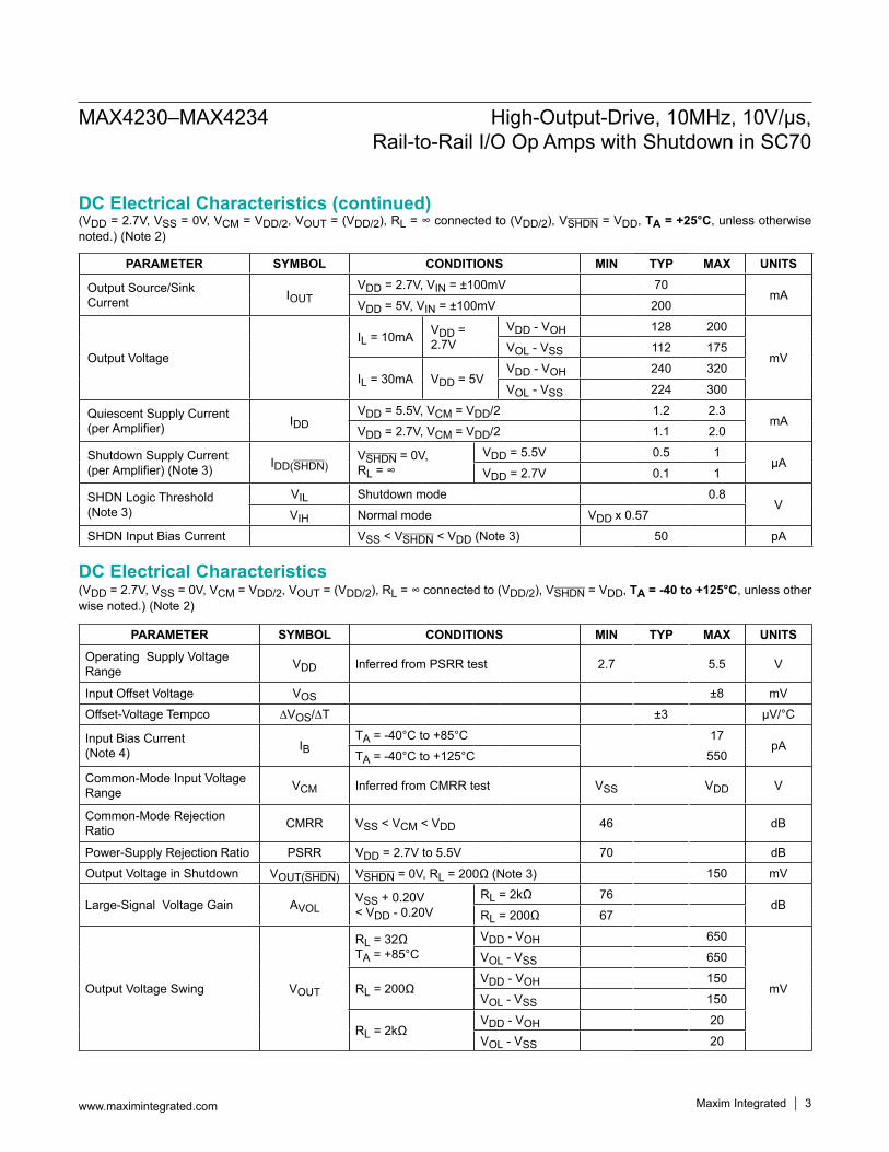
For example, the circuit in Figure 1 has a package power dissipation of 196mW:
PEAKDD DC
RMS
PEAKRMS DC
RMS
VRMS (V V )2
1.0V3.6V 1.8V 2.507V2
I 1.8V 1.0V / 32I I322 2
78.4mA
≅ − +
= − + =
Ω≅ + = +
Ω=
where:VDC = the DC component of the output voltage.IDC = the DC component of the output current.VPEAK = the highest positive excursion of the AC compo-nent of the output voltage.IPEAK = the highest positive excursion of the AC compo-nent of the output current.Therefore:
IC(DISS) RMS RMSP = V I COS
= 196mW
θ
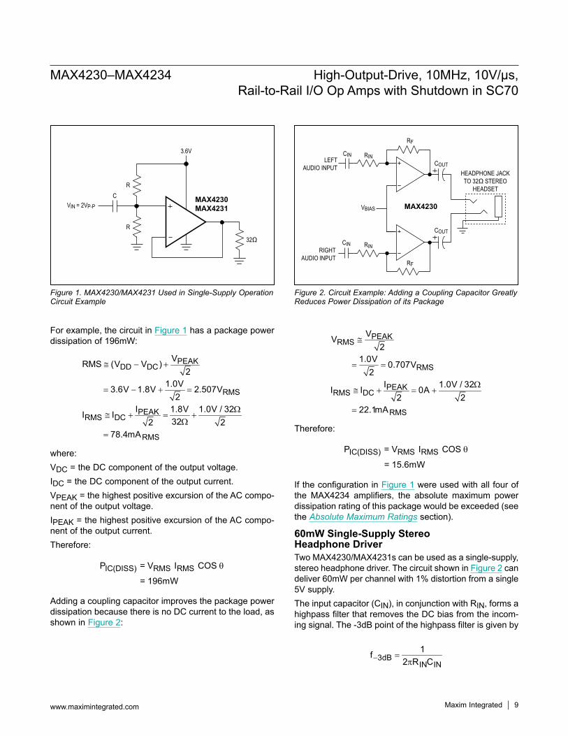
Adding a coupling capacitor improves the package power dissipation because there is no DC current to the load, as shown in Figure 2:
PEAKRMS
RMS
PEAKRMS DC
RMS
VV2
1.0V 0.707V2
I 1.0V / 32I I 0A2 2
22.1mA
≅
= =
Ω≅ + = +
=
Therefore:
IC(DISS) RMS RMSP = V I COS
= 15.6mW
θ
If the configuration in Figure 1 were used with all four of the MAX4234 amplifiers, the absolute maximum power dissipation rating of this package would be exceeded (see the Absolute Maximum Ratings section).
60mW Single-Supply Stereo Headphone DriverTwo MAX4230/MAX4231s can be used as a single-supply, stereo headphone driver. The circuit shown in Figure 2 can deliver 60mW per channel with 1% distortion from a single 5V supply.The input capacitor (CIN), in conjunction with RIN, forms a highpass filter that removes the DC bias from the incom-ing signal. The -3dB point of the highpass filter is given by
3dBIN IN
1f2 R C− =π
Figure 1. MAX4230/MAX4231 Used in Single-Supply Operation Circuit Example
Figure 2. Circuit Example: Adding a Coupling Capacitor Greatly Reduces Power Dissipation of its Package
3.6V
VIN = 2VP-P
R
C
32Ω
R
MAX4230MAX4231
RIGHTAUDIO INPUT
LEFTAUDIO INPUT
CIN
CIN RIN
RIN
RF
COUT
VBIAS
HEADPHONE JACKTO 32Ω STEREO
HEADSET
RF
MAX4230
COUT
MAX4230–MAX4234 High-Output-Drive, 10MHz, 10V/μs, Rail-to-Rail I/O Op Amps with Shutdown in SC70
www.maximintegrated.com Maxim Integrated 9

Choose gain-setting resistors RIN and RF according to the amount of desired gain, keeping in mind the maximum output amplitude. The output coupling capacitor, COUT, blocks the DC component of the amplifier output, prevent-ing DC current flowing to the load. The output capacitor and the load impedance form a highpass filer with the -3dB point determined by:
3dBIN OUT
1f2 R C− =π
For a 32Ω load, a 100μF aluminum electrolytic capacitor gives a low-frequency pole at 50Hz.
Bridge AmplifierThe circuit shown in Figure 3 uses a dual MAX4230 to implement a 3V, 200mW amplifier suitable for use in size-constrained applications. This configuration eliminates the need for the large coupling capacitor required by the single op-amp speaker driver when single-supply opera-tion is necessary. Voltage gain is set to 10V/V; however, it can be changed by adjusting the 82kΩ resistor value.
Rail-to-Rail Input StageThe MAX4230–MAX4234 CMOS op amps have parallel connected n- and p-channel differential input stages that combine to accept a common-mode range extending to both supply rails. The n-channel stage is active for common-mode input voltages typically greater than (VSS + 1.2V), and the p-channel stage is active for common-mode input voltages typically less than (VDD -1.2V).
Rail-to-Rail Output StageThe minimum output is within millivolts of ground for single-supply operation, where the load is referenced to ground (VSS). Figure 4 shows the input voltage range and the output voltage swing of a MAX4230 connected as a voltage follower. The maximum output voltage swing is load dependent; however, it is guaranteed to be within 500mV of the positive rail (VDD = 2.7V) even with maxi-mum load (32Ω to ground).Observe the Absolute Maximum Ratings for power dis-sipation and output short-circuit duration (10s, max)because the output current can exceed 200mA (see the Typical Operating Characteristics.)
Input CapacitanceOne consequence of the parallel-connected differential input stages for rail-to-rail operation is a relatively large input capacitance CIN (5pF typ). This introduces a pole at frequency (2πR′CIN)-1, where R′ is the parallel com-bination of the gain-setting resistors for the inverting or noninverting amplifier configuration (Figure 5). If the pole frequency is less than or comparable to the unity-gain bandwidth (10MHz), the phase margin is reduced, and the amplifier exhibits degraded AC performance through either ringing in the step response or sustained oscilla-tions. The pole frequency is 10MHz when R′ = 2kΩ. To maximize stability, R′ << 2kΩ is recommended.
Figure 3. Dual MAX4230/MAX4231 Bridge Amplifier for 200mW at 3V
Figure 4. Rail-to-Rail Input/Output Range
1
67
5
2 83V3V
3 4
1/2MAX4232
1/2MAX4232
0.5VP-P
R551kΩ
R116kΩ
R282kΩ
R410kΩ
32WfS = 100Hz
R310kΩ
R651kΩ
C20.1µF
C10.1mF
IN1V/div
OUT1V/div
5µs/div
VCC = 3.0VRL = 100kΩ
MAX4230–MAX4234 High-Output-Drive, 10MHz, 10V/μs, Rail-to-Rail I/O Op Amps with Shutdown in SC70
www.maximintegrated.com Maxim Integrated 10

To improve step response when R′ > 2kΩ, connect small capacitor Cf between the inverting input and output.Choose Cf as follows:
Cf = 8(R/Rf) [pf]where Rf is the feedback resistor and R is the gain-setting resistor (Figure 5).
Driving Capacitive LoadsThe MAX4230–MAX4234 have a high tolerance for capacitive loads. They are stable with capacitive loads up to 780pF. Figure 6 is a graph of the stable operating region for various capacitive loads vs. resistive loads.Figures 7 and 8 show the transient response with excessive capaci-tive loads (1500pF), with and without the addition of an isolation resistor in series with the output. Figure 9 shows a typical noninverting capacitive-load-driving circuit in the unity-gain configuration.
Figure 6. Capacitive-Load Stability
Figure 7. Small-Signal Transient Response with Excessive Capacitive Load
Figure 8. Small-Signal Transient Response with Excessive Capacitive Load with Isolation Resistor
Figure 5. Inverting and Noninverting Amplifiers with Feedback Compensation
0
500
1500
1000
2000
2500
1 10010 1k 10k 100kRESISTIVE LOAD (Ω)
CAPA
CITI
VE LO
AD (p
F)
VDD = 5.0VRL TO VDD/2
STABLE
UNSTABLE
1µ/div
20mV/div
20mV/divVDD = 3.0V, CL = 1500pFRL = 100kΩ, RISO = 0Ω
1µ/div
20mV/div
20mV/divVDD = 3.0V, CL = 1500pFRL = 100kΩ, RISO = 39Ω
MAX4230VIN
VOUT
R’ = R || RfRfCf = RCIN
Rf
Cf
R
INVERTING
MAX4230VIN
VOUT
R’ = R || RfRfCf = RCIN
Rf
R
Cf
NONINVERTING
MAX4230–MAX4234 High-Output-Drive, 10MHz, 10V/μs, Rail-to-Rail I/O Op Amps with Shutdown in SC70
www.maximintegrated.com Maxim Integrated 11
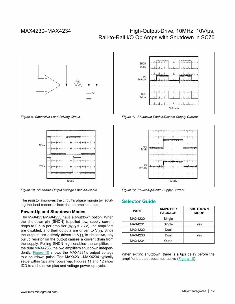
The resistor improves the circuit’s phase margin by isolat-ing the load capacitor from the op amp’s output.
Power-Up and Shutdown ModesThe MAX4231/MAX4233 have a shutdown option. When the shutdown pin (SHDN) is pulled low, supply current drops to 0.5μA per amplifier (VDD = 2.7V), the amplifiers are disabled, and their outputs are driven to VSS. Since the outputs are actively driven to VSS in shutdown, any pullup resistor on the output causes a current drain from the supply. Pulling SHDN high enables the amplifier. In the dual MAX4233, the two amplifiers shut down indepen-dently. Figure 10 shows the MAX4231’s output voltage to a shutdown pulse. The MAX4231–MAX4234 typically settle within 5μs after power-up. Figures 11 and 12 show IDD to a shutdown plus and voltage power-up cycle.
When exiting shutdown, there is a 6μs delay before the amplifier’s output becomes active (Figure 10).
Figure 9. Capacitive-Load-Driving Circuit Figure 11. Shutdown Enable/Disable Supply Current
Figure 10. Shutdown Output Voltage Enable/Disable Figure 12. Power-Up/Down Supply Current
PART AMPS PER PACKAGE
SHUTDOWN MODE
MAX4230 Single —MAX4231 Single YesMAX4232 Dual —MAX4233 Dual YesMAX4234 Quad —
RISO
CL
100µs/div
SHDN2V/div
IDD1mA/div
OUT2V/div
4µs/div
1V/div
1V/div
40µs/div
VDD2V/div
IDD1mA/div
MAX4230–MAX4234 High-Output-Drive, 10MHz, 10V/μs, Rail-to-Rail I/O Op Amps with Shutdown in SC70
www.maximintegrated.com Maxim Integrated 12
Selector Guide
Power Supplies and LayoutThe MAX4230–MAX4234 can operate from a single 2.7V to 5.5V supply, or from dual ±1.35V to ±2.5V supplies. or single-supply operation, bypass the power supply with a 0.1μF ceramic capacitor. For dual-supply operation, bypass each supply to ground. Good layout improves performance by decreasing the amount of stray capacitance at the op amps’ inputs and outputs. Decrease stray capacitance by placing external components close to the op amps’ pins, minimizing trace and lead lengths.
+Denotes a lead-free(Pb)/RoHS-compliant package.T = Tape and reel./V denotes an automotive-qualified part. *EP = Exposed pad.
PART TEMP RANGE
PIN-PACKAGE
TOP MARK
MAX4232AKA+T -40°C to +125°C 8 SOT23 AAKWMAX4232AKA/V+T -40°C to +125°C 8 SOT23 AEQWMAX4232AUA+T -40°C to +125°C 8 μMAX —MAX4233AUB+T -40°C to +125°C 10 μMAX —MAX4233ABC+T -40°C to +125°C 10 UCSP ABFMAX4234AUD -40°C to +125°C 14 TSSOP —
MAX4234AUD/V+T -40°C to +125°C 14 TSSOP —MAX4234ASD -40°C to +125°C 14 SO —
TOP VIEW
IN2-
IN2+VSS
1
2
8
7
VDD
OUT2IN1-
IN1+
OUT1
SOT23/MAX
3
4
6
5
MAX4232
1
2
3
4
5
10
9
8
7
6
VDD
OUT2
IN2-
IN2+VSS
IN1+
IN1-
OUT1
MAX4233
MAX
SHDN2SHDN1
VSS
OUTIN-
1 6 VDD
5
IN+
SC70/SOT23
2
3 4
SHDN
MAX4231
14
13
12
11
10
9
8
1
2
3
4
5
6
7
OUT4
IN4-
IN4+
VSSVDD
IN1+
IN1-
OUT1
MAX4234
IN3+
IN3-
OUT3OUT2
IN2-
IN2+
TSSOP/SO
VSS
OUTIN-
1 5 VDDIN+
MAX4230
SOT23/SC70
2
3 4
OUT1
VDD
OUT2
IN1-
IN2-
IN1+
IN2+
VSS
UCSP
MAX4233
SHDN1
SHDN2
1 2 3 4
A
B
CIN+
VSS
IN-
OUT VDD
UCSP
MAX4231
1 2 3
A
B
1 2 3
456
VDD OUT
IN+ IN-VSS
MAX4231
Thin µDFN(Ultra-Thin LGA)
SHDN
+
+ +
+
+
+
SHDN
MAX4230–MAX4234 High-Output-Drive, 10MHz, 10V/μs, Rail-to-Rail I/O Op Amps with Shutdown in SC70
www.maximintegrated.com Maxim Integrated 13
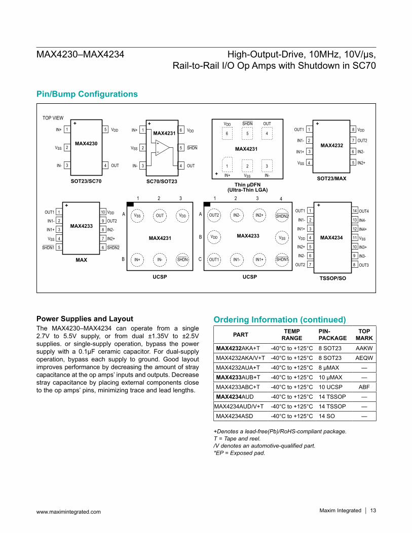
Pin/Bump Configurations
Ordering Information (continued)
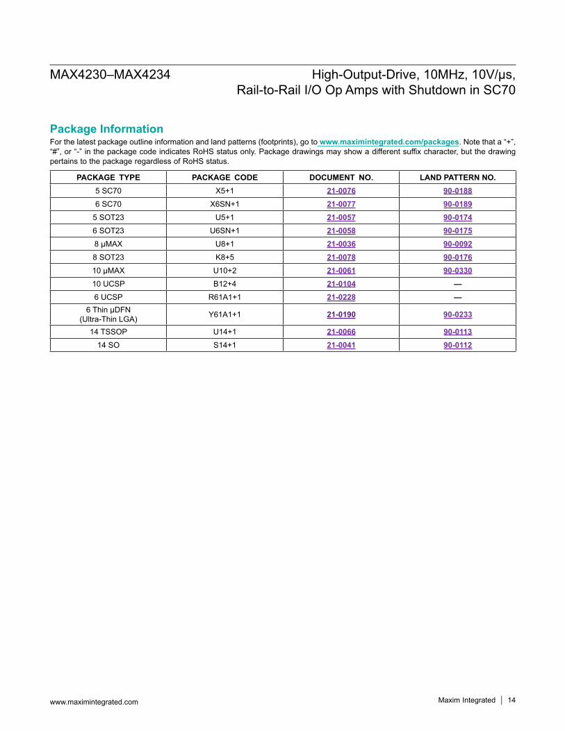
PACKAGE TYPE PACKAGE CODE DOCUMENT NO. LAND PATTERN NO.5 SC70 X5+1 21-0076 90-01886 SC70 X6SN+1 21-0077 90-0189
5 SOT23 U5+1 21-0057 90-01746 SOT23 U6SN+1 21-0058 90-01758 μMAX U8+1 21-0036 90-00928 SOT23 K8+5 21-0078 90-017610 μMAX U10+2 21-0061 90-033010 UCSP B12+4 21-0104 —6 UCSP R61A1+1 21-0228 —
6 Thin μDFN (Ultra-Thin LGA) Y61A1+1 21-0190 90-0233
14 TSSOP U14+1 21-0066 90-011314 SO S14+1 21-0041 90-0112
MAX4230–MAX4234 High-Output-Drive, 10MHz, 10V/μs, Rail-to-Rail I/O Op Amps with Shutdown in SC70
www.maximintegrated.com Maxim Integrated 14
Package InformationFor the latest package outline information and land patterns (footprints), go to www.maximintegrated.com/packages. Note that a “+”, “#”, or “-” in the package code indicates RoHS status only. Package drawings may show a different suffix character, but the drawing pertains to the package regardless of RoHS status.

REVISION NUMBER
REVISION DATE DESCRIPTION PAGES
CHANGED7 7/08 Added 6-pin μDFN package for the MAX4231 1, 2, 8, 13
8 10/08 Corrected top mark for MAX4321, 6 SOT23 package; changed MAX4320 and 4321 to lead-free packages 1
9 10/08 Added shutdown pin limits 3, 410 12/08 Added automotive part number 1311 9/09 Corrected top mark designation and pin configuration, and added UCSP package 1, 2, 8, 1312 1/10 Updated Absolute Maximum Ratings section 213 1/11 Added 10 μMAX to Package Information section 14
14 10/11 Updated Electrical Characteristics table with specs for bias current at various temperatures 1–4
15 3/12 Updated thermal data in the Absolute Maximum Ratings 216 6/12 Added automotive part number for MAX4230 117 12/13 Updated tENABLE specification in the AC Electrical Characteristics 6
18 10/14 Corrected µDFN references and added ultra-thin LGA reference to Ordering Information, Pin Configurations, and Package Information 1, 13, 14
19 1/15 Updated General Description, Applications, and Benefits and Features sections 120 11/16 Updated TOC22 in Typical Operating Characteristics section 721 2/18 Updated Benefits and Features section and Ordering Information table 1, 13
Maxim Integrated cannot assume responsibility for use of any circuitry other than circuitry entirely embodied in a Maxim Integrated product. No circuit patent licenses are implied. Maxim Integrated reserves the right to change the circuitry and specifications without notice at any time. The parametric values (min and max limits) shown in the Electrical Characteristics table are guaranteed. Other parametric values quoted in this data sheet are provided for guidance.
Maxim Integrated and the Maxim Integrated logo are trademarks of Maxim Integrated Products, Inc.
MAX4230–MAX4234 High-Output-Drive, 10MHz, 10V/μs, Rail-to-Rail I/O Op Amps with Shutdown in SC70
© 2018 Maxim Integrated Products, Inc. 15
Revision History
For pricing, delivery, and ordering information, please contact Maxim Direct at 1-888-629-4642, or visit Maxim Integrated’s website at www.maximintegrated.com.