
Mask Metrology and Pattern Profile Analysis Using the AIT: Down to 65 nm · Mask Metrology and...
42
Mask Metrology and Pattern Profile Analysis Using the AIT: Down to 65 nm I. Mochi, K. A. Goldberg Lawrence Berkeley National Laboratory Tom Wallow GlobalFoundries 2010 International Workshop on EUV Lithography
Transcript of Mask Metrology and Pattern Profile Analysis Using the AIT: Down to 65 nm · Mask Metrology and...
Mask Metrology and Pattern Profile Analysis Using the AIT: Down to 65 nm
I. Mochi, K. A. GoldbergLawrence Berkeley National Laboratory
Tom WallowGlobalFoundries
2010 International Workshop on EUV Lithography
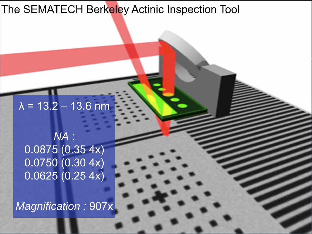
The SEMATECH Berkeley Actinic Inspection Tool
λ = 13.2 – 13.6 nm
NA :0.0875 (0.35 4x)0.0750 (0.30 4x)0.0625 (0.25 4x)
Magnification : 907x

Phase roughness
BossungNILSContrast
λsensitivity
Phase defects
LER Defect inspection
OPC Correction
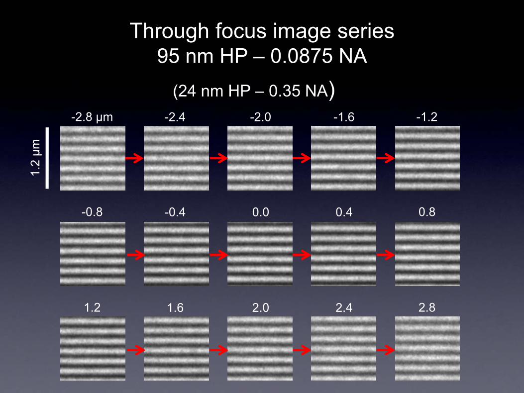
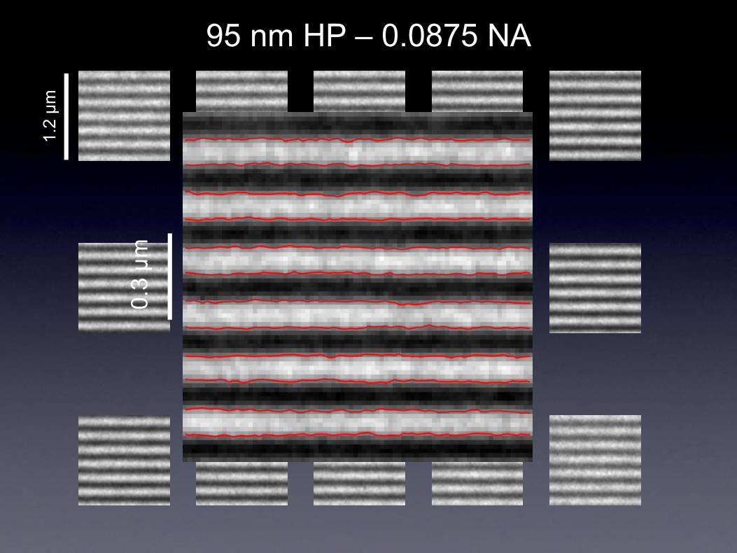
Through focus image series95 nm HP – 0.0875 NA
-2.8 µm -2.4 -2.0 -1.6 -1.2
-0.8 -0.4 0.0 0.4 0.8
1.2 1.6 2.0 2.4 2.8
1.2
µm
(24 nm HP – 0.35 NA)
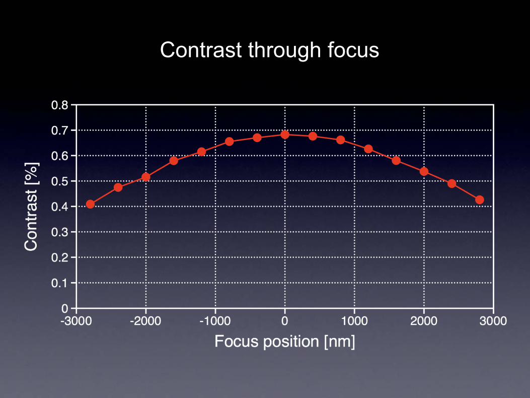
Contrast through focus
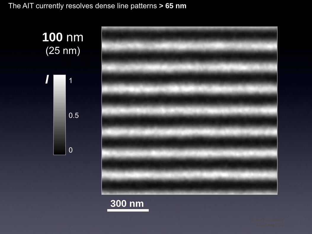
The AIT currently resolves dense line patterns > 65 nm
100 nm(25 nm)
GlobalFoundriesMask MET10
300 nm
I 1
0.5
0
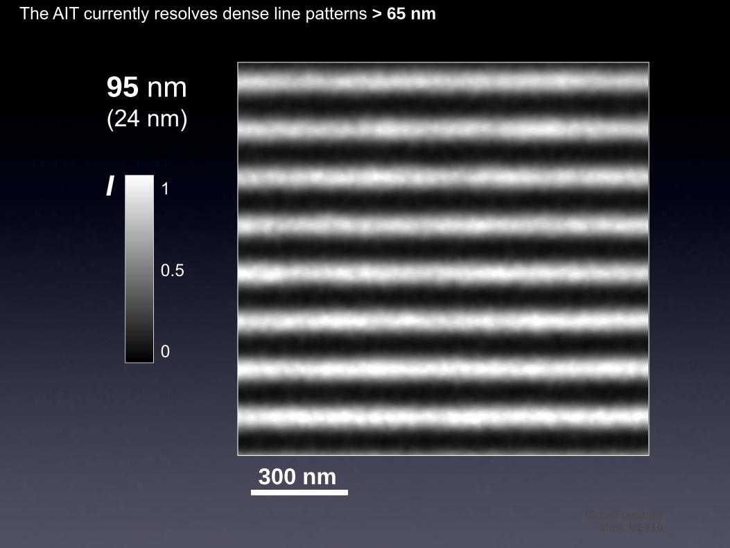
The AIT currently resolves dense line patterns > 65 nm
95 nm(24 nm)
GlobalFoundriesMask MET10
300 nm
I 1
0.5
0
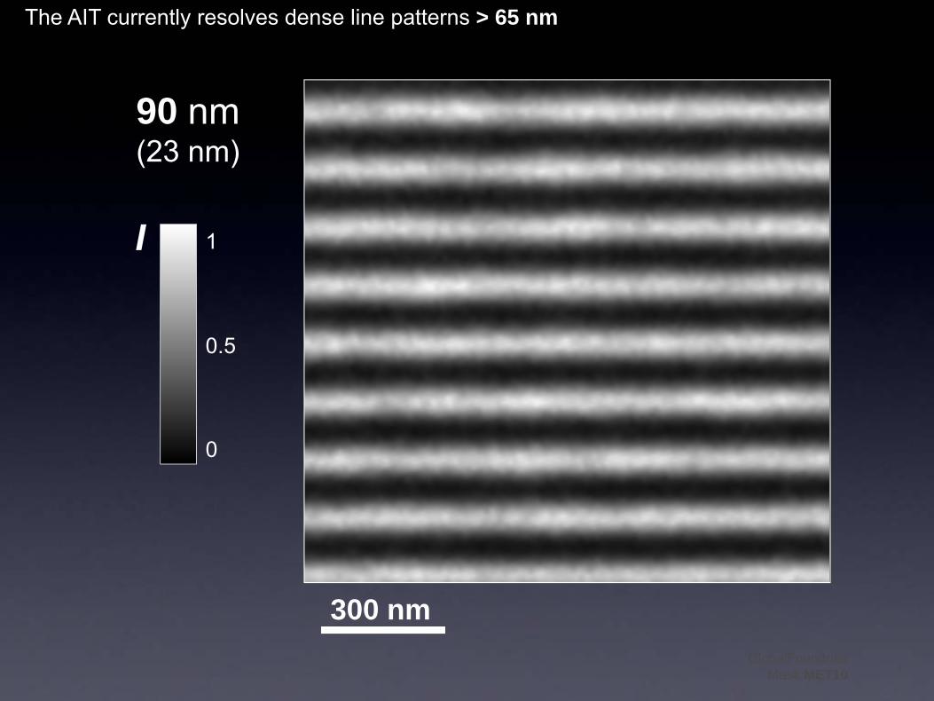
The AIT currently resolves dense line patterns > 65 nm
90 nm (23 nm)
GlobalFoundriesMask MET10
300 nm
I 1
0.5
0
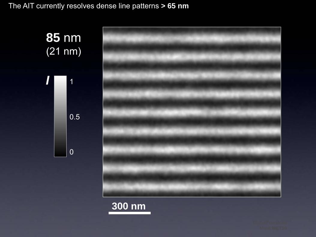
The AIT currently resolves dense line patterns > 65 nm
85 nm(21 nm)
GlobalFoundriesMask MET10
300 nm
I 1
0.5
0
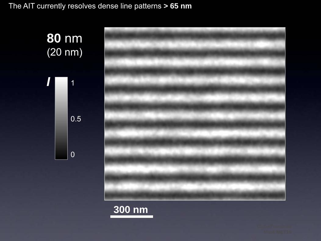
The AIT currently resolves dense line patterns > 65 nm
80 nm(20 nm)
GlobalFoundriesMask MET10
300 nm
I 1
0.5
0
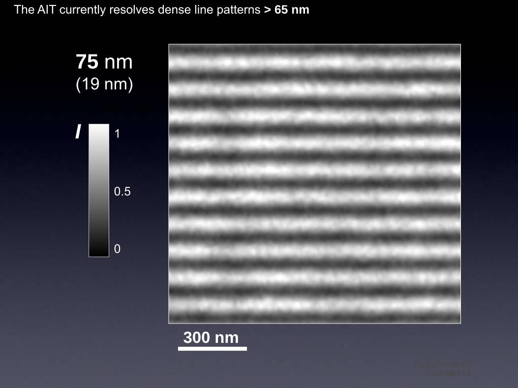
The AIT currently resolves dense line patterns > 65 nm
75 nm(19 nm)
GlobalFoundriesMask MET10
300 nm
I 1
0.5
0
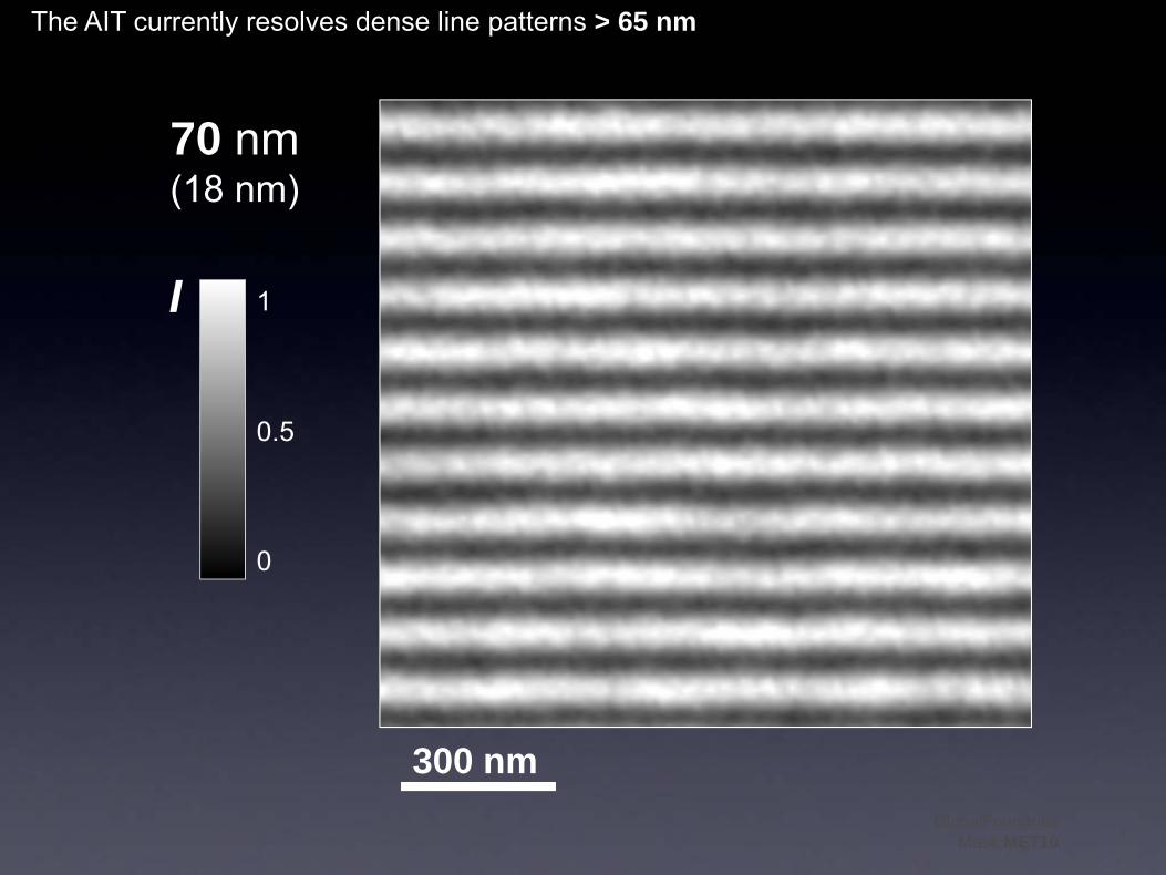
The AIT currently resolves dense line patterns > 65 nm
70 nm(18 nm)
GlobalFoundriesMask MET10
300 nm
I 1
0.5
0
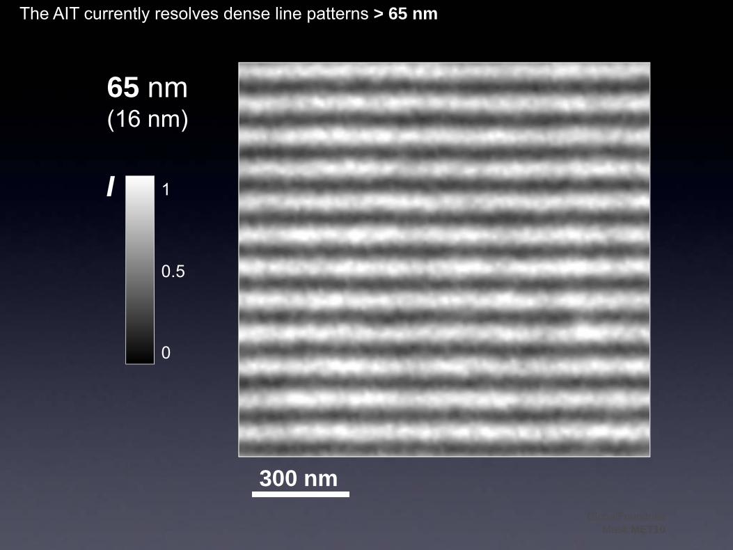
The AIT currently resolves dense line patterns > 65 nm
65 nm(16 nm)
GlobalFoundriesMask MET10
300 nm
I 1
0.5
0
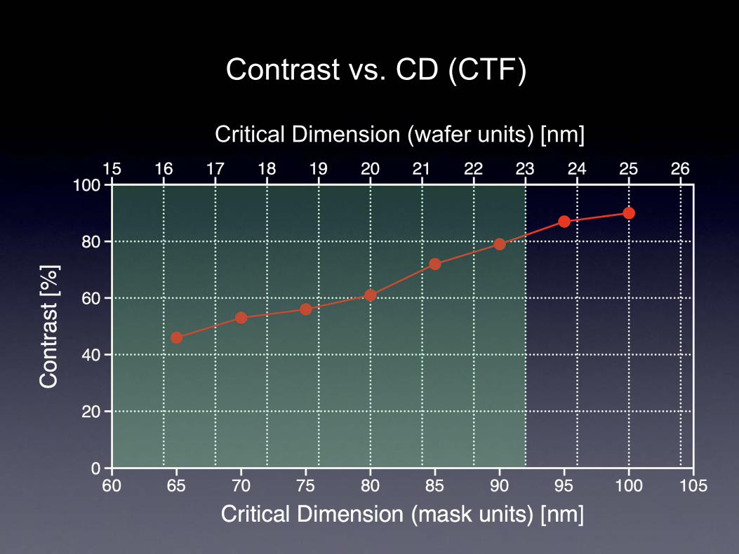
Critical Dimension (wafer units) [nm]
Contrast vs. CD (CTF)

Phase roughness
BossungNILSContrast
λsensitivity
Phase defects
LER Defect inspection
OPC Correction
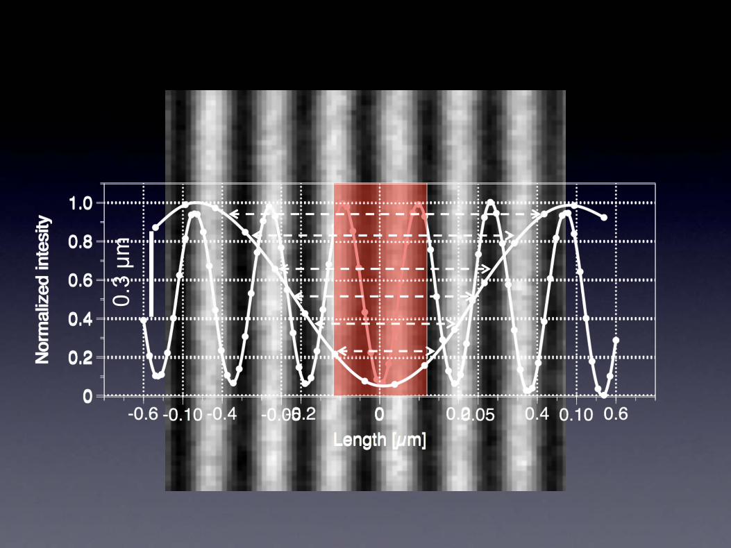
0.3
µm
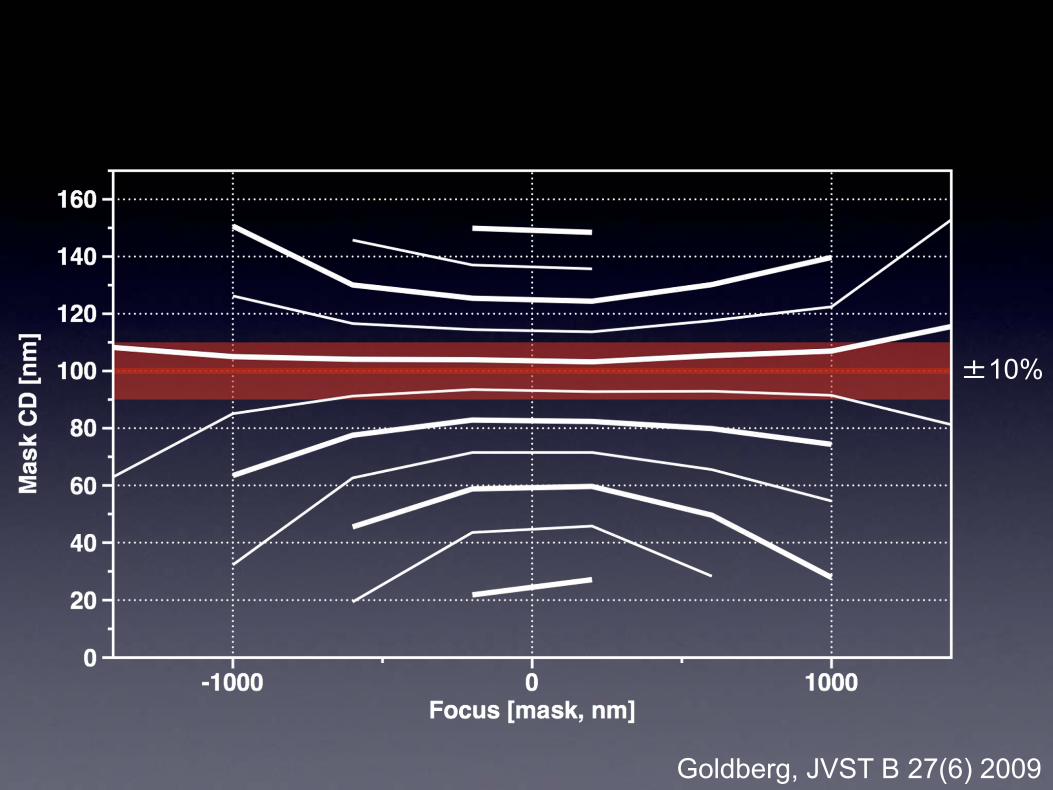
Goldberg, JVST B 27(6) 2009
±10%

Phase roughness
BossungNILSContrast
λsensitivity
Phase defects
LER Defect inspection
OPC Correction
95 nm HP – 0.0875 NA1.
2 µm
0.3
µm
Photon flux requirements for EUV reticle imaging microscopy in the 22- and 16nm nodesDaniel T. Wintz, Kenneth A. Goldberg, Iacopo Mochi, and Sungmin Huh, Proc. SPIE 7636, 76362L (2010)
How many photons do we need?

Phase roughness
BossungNILSContrast
λsensitivity
Phase defects
LER Defect inspection
OPC Correction
1µm
1µm 1µm
1µm 1µm
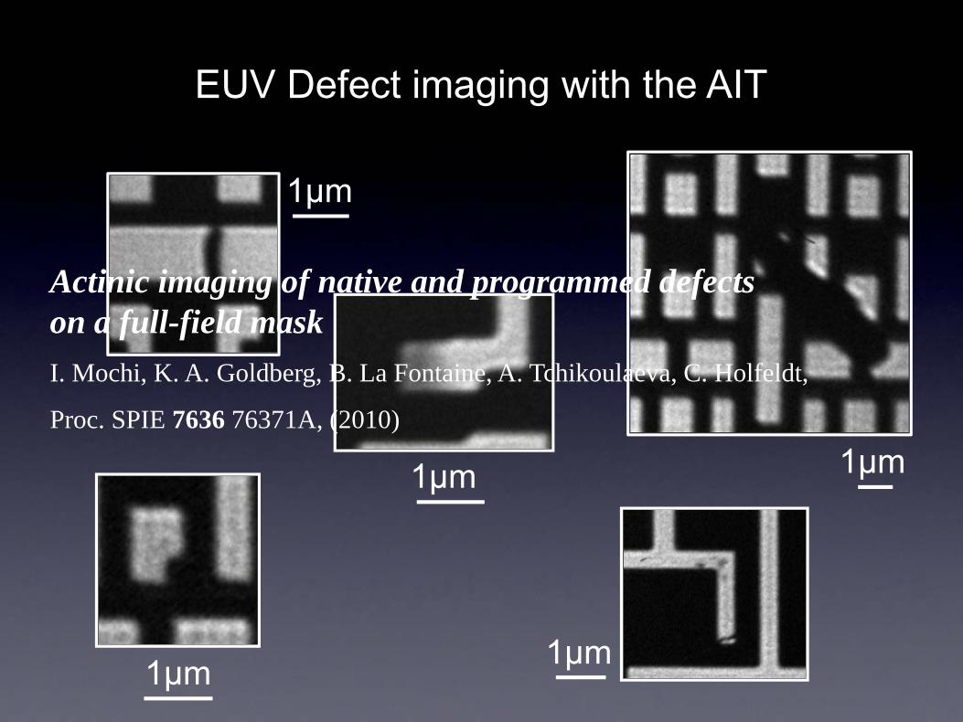
EUV Defect imaging with the AIT
Actinic imaging of native and programmed defectson a full-field maskI. Mochi, K. A. Goldberg, B. La Fontaine, A. Tchikoulaeva, C. Holfeldt,
Proc. SPIE 7636 76371A, (2010)
Phase roughness
BossungNILSContrast
λsensitivity
Phase defects
LER Defect inspection
OPC Correction
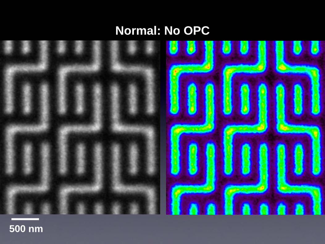
Normal: No OPC
500 nm
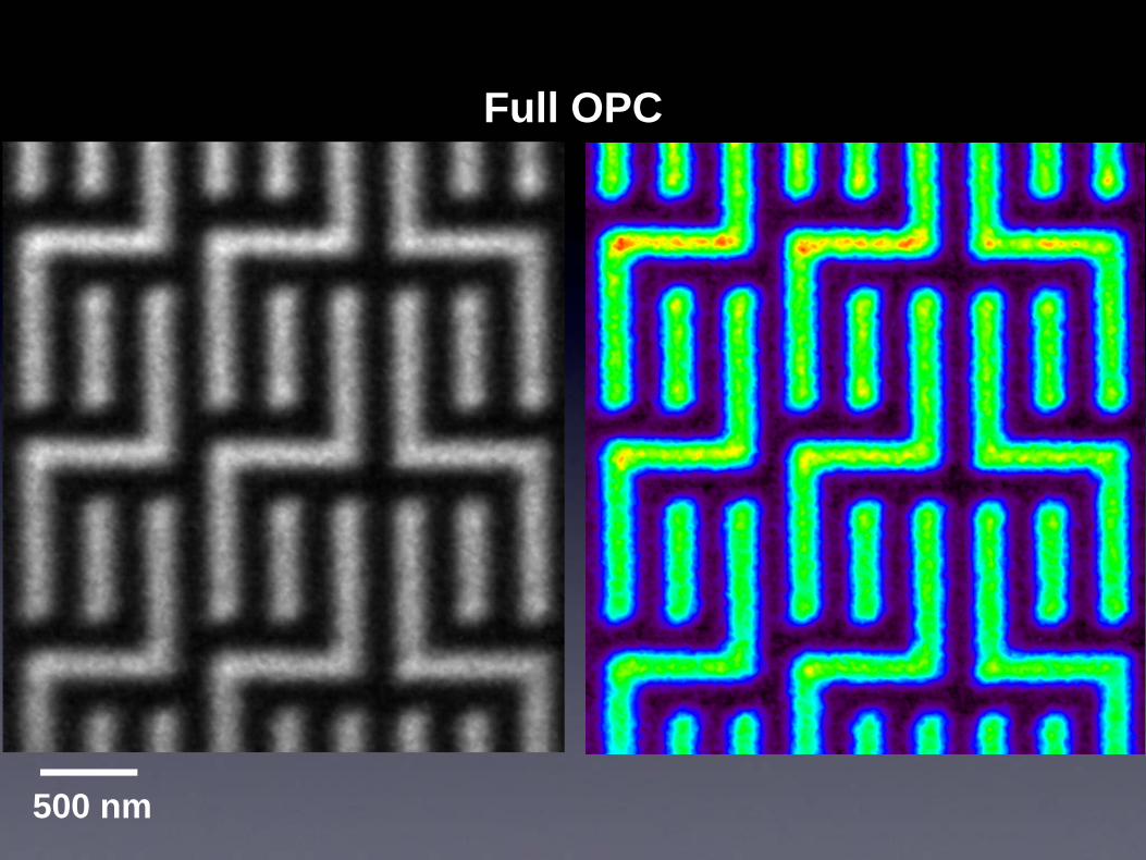
Full OPC
500 nm

Phase roughness
BossungNILSContrast
λsensitivity
Phase defects
LER Defect inspection
OPC Correction
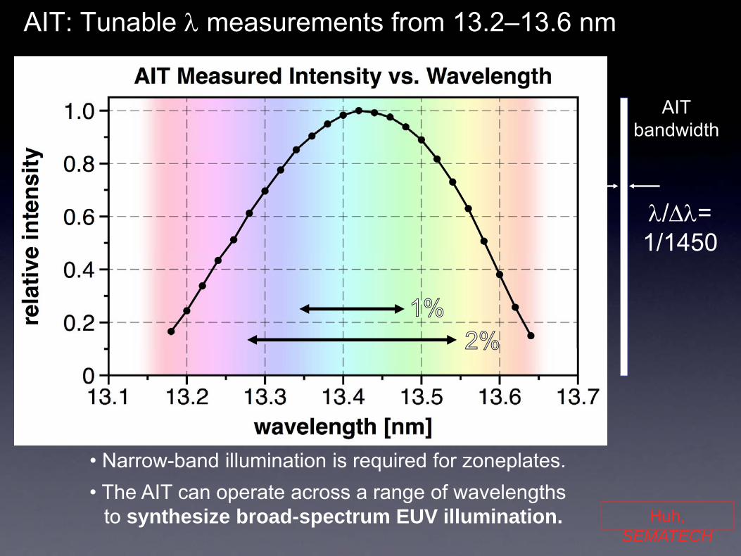
AIT: Tunable λ measurements from 13.2–13.6 nm
λ/Δλ=1/1450
AITbandwidth
• Narrow-band illumination is required for zoneplates.• The AIT can operate across a range of wavelengths
to synthesize broad-spectrum EUV illumination. Huh, SEMATECH
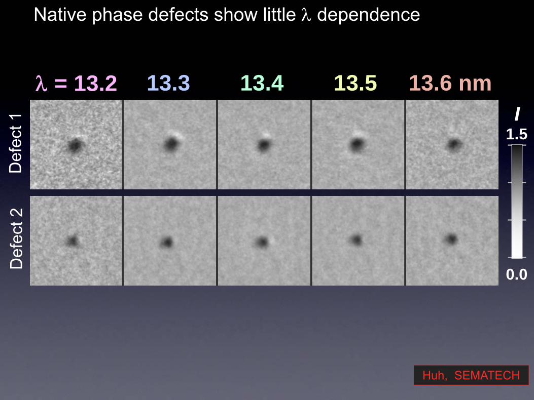
Native phase defects show little λ dependence
1.5
0.0
I
Def
ect V
Def
ect X
Def
ect 1
Def
ect 2
λ = 13.2 13.3 13.4 13.5 13.6 nm
Huh, SEMATECH

Phase roughness
BossungNILSContrast
λsensitivity
Phase defects
LER Defect inspection
OPC Correction
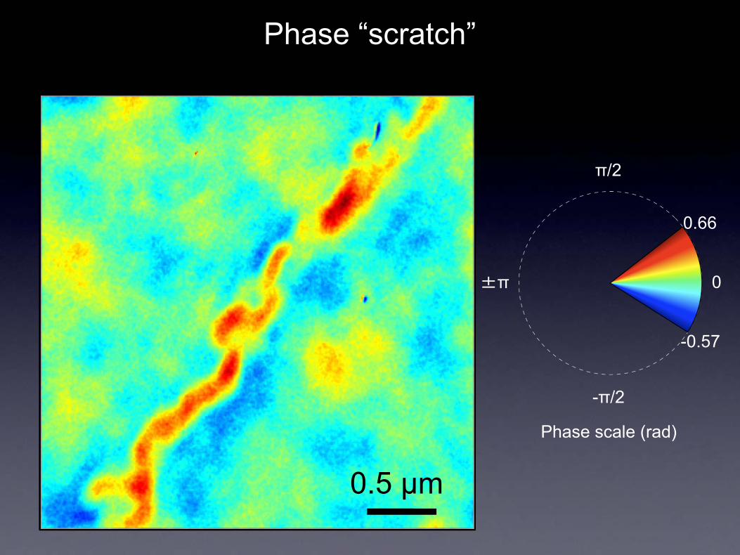
Phase “scratch”
π/2
0±π
-π/2
-0.57
0.66
Phase scale (rad)
0.5 µm
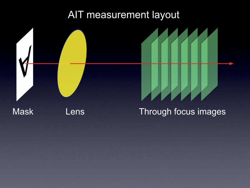
LensMask Through focus images
AIT measurement layout
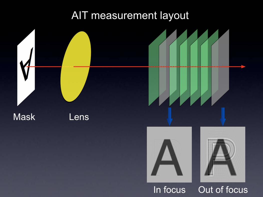
LensMask
In focus Out of focus
AIT measurement layout
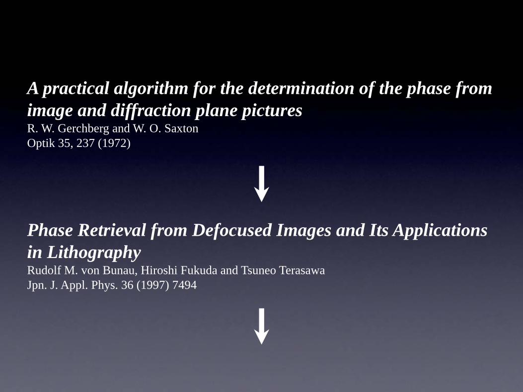
Phase Retrieval from Defocused Images and Its Applications in LithographyRudolf M. von Bunau, Hiroshi Fukuda and Tsuneo TerasawaJpn. J. Appl. Phys. 36 (1997) 7494
A practical algorithm for the determination of the phase from image and diffraction plane picturesR. W. Gerchberg and W. O. SaxtonOptik 35, 237 (1972)
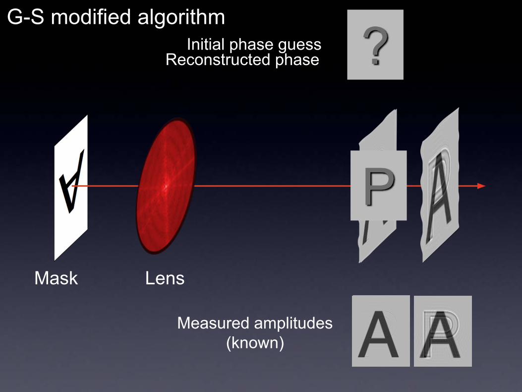
?Initial phase guess
Measured amplitudes(known)
Reconstructed phase
LensMask
G-S modified algorithm
P
In focus Out of focus
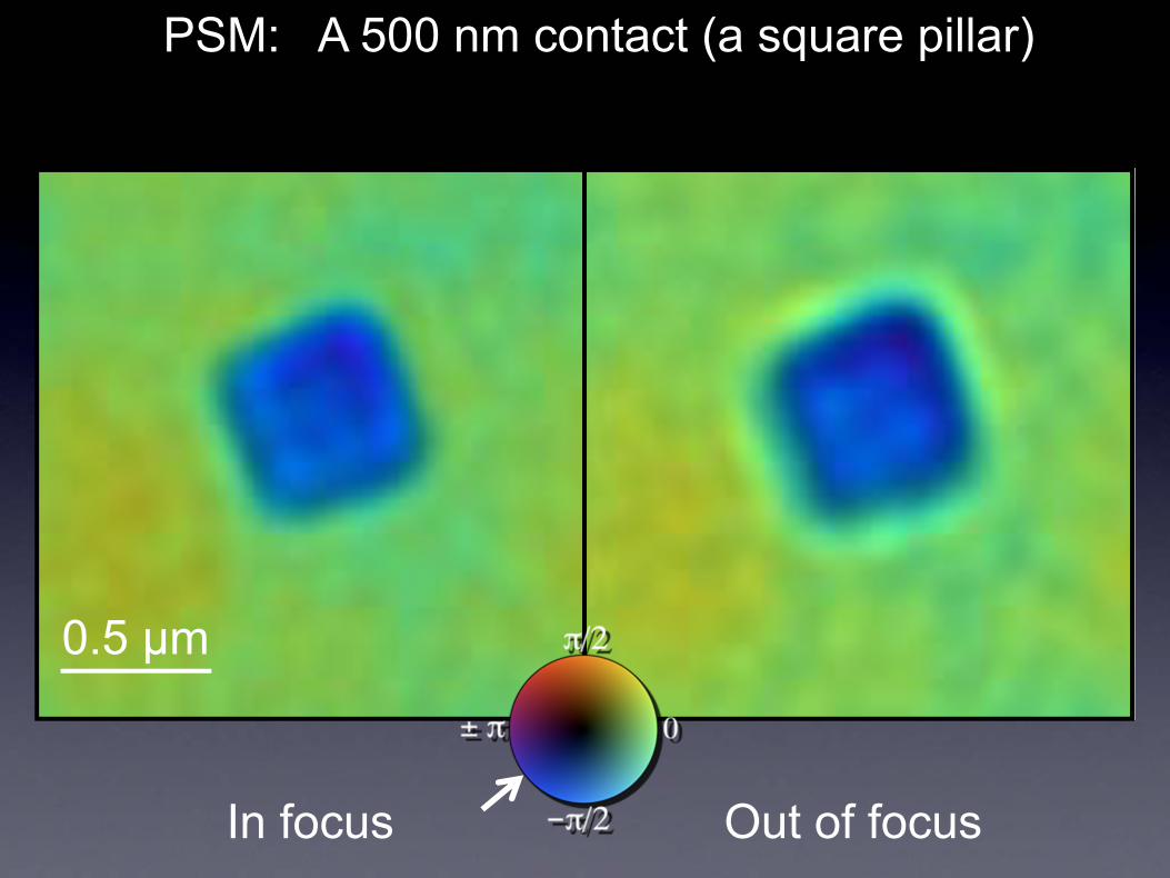
PSM: A 500 nm contact (a square pillar)
0.5 µm0.5 µm
In focus Out of focus
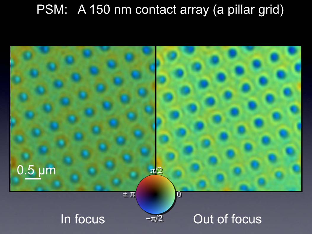
PSM: A 150 nm contact array (a pillar grid)
0.5 µm
In focus Out of focus
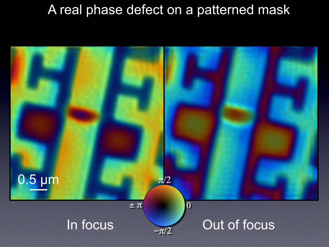
0.5 µm
A real phase defect on a patterned mask
In focus Out of focus
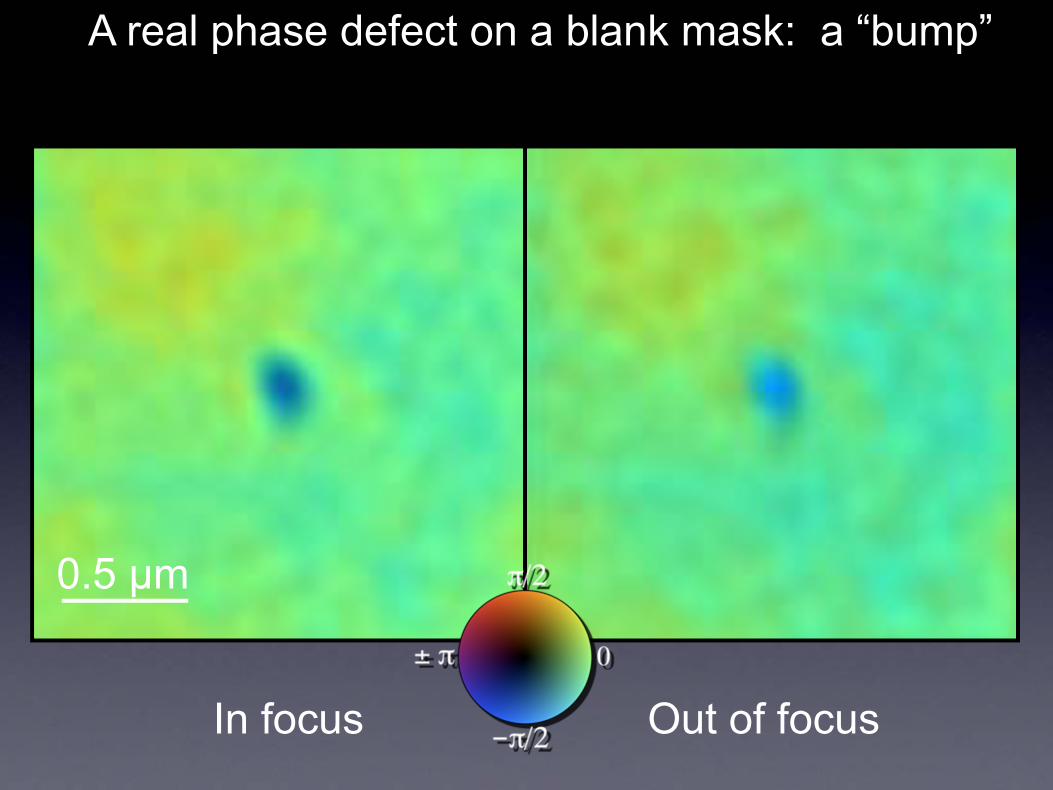
A real phase defect on a blank mask: a “bump”
0.5 µm

Phase roughness
BossungNILSContrast
λsensitivity
Phase defects
LER Defect inspection
OPC Correction
π/2
-π/2
0
0.39
-0.36
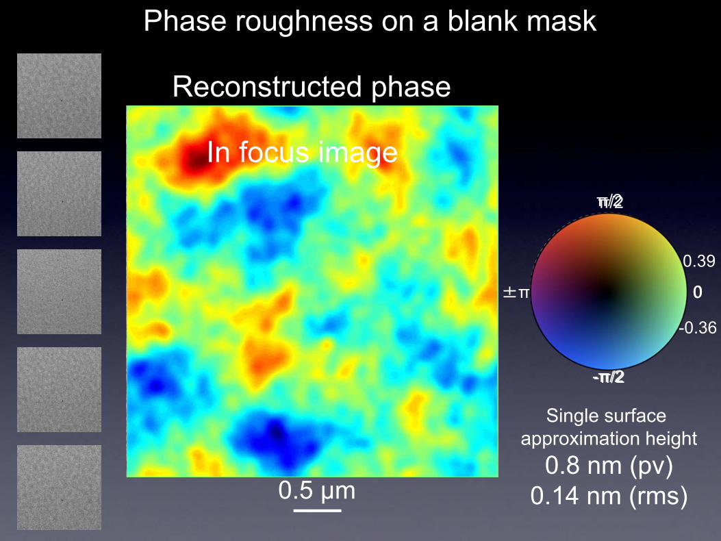
Phase roughness on a blank mask
π/2
-π/2
0±π
Reconstructed phase
0.5 µm
In focus image
Single surface approximation height
0.8 nm (pv)0.14 nm (rms)
Conclusion
This work was supported by SEMATECH, through the U.S. Department of Energy under Contract No. DE-AC02-05CH11231
Phase roughness
BossungNILSContrast
λsensitivity
Phase defects
LER Defect inspection
OPC Correction
Acknowledgements
Kenji Yamazoe – CanonAndy Neureuther, Chris Clifford – UC BerkeleySungmin Huh – SamsungSimi George, Patrick Naulleau – LBNL
AIT.lbl.gov


![Stealth Force 8.0 SZ - mayagraphics.gr · [ Spider 8.1 Hydro HPi ] [ Spider 8.1 Multicam HPi ] [ Spider 8.1 Desert HPi ] ion mask™ επεξεργασία με νανοτεχνολογία](https://static.fdocument.org/doc/165x107/5e0b1618b9afd121e77d5fd1/stealth-force-80-sz-spider-81-hydro-hpi-spider-81-multicam-hpi-spider.jpg)
