MANUAL DE INSTALACIÓN ``MONITOR …TULO 3. PROCEDIMIENTO 16 d) Ubicar en el área de trabajo el...
42
Transcript of MANUAL DE INSTALACIÓN ``MONITOR …TULO 3. PROCEDIMIENTO 16 d) Ubicar en el área de trabajo el...

MANUAL DE INSTALACIÓN MONITOR PERMANENTE DETEMPERATURA(MPT)
1
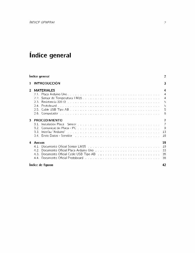
ÍNDICE GENERAL 2
Índice general
Índice general 2
1 INTRODUCCIÓN 3
2 MATERIALES 42.1. Placa Arduino Uno . . . . . . . . . . . . . . . . . . . . . . . . . . . . . . . . . . . . . 42.2. Sensor de Temperatura LM35 . . . . . . . . . . . . . . . . . . . . . . . . . . . . . . . 42.3. Resistencia 220 Ω . . . . . . . . . . . . . . . . . . . . . . . . . . . . . . . . . . . . . 52.4. Protoboard . . . . . . . . . . . . . . . . . . . . . . . . . . . . . . . . . . . . . . . . . 52.5. Cable USB Tipo AB . . . . . . . . . . . . . . . . . . . . . . . . . . . . . . . . . . . . 52.6. Computador . . . . . . . . . . . . . . . . . . . . . . . . . . . . . . . . . . . . . . . . 6
3 PROCEDIMIENTO 73.1. Instalación Placa - Sensor . . . . . . . . . . . . . . . . . . . . . . . . . . . . . . . . . 73.2. Comunicación Placa - PC . . . . . . . . . . . . . . . . . . . . . . . . . . . . . . . . . 93.3. Interfaz Arduino . . . . . . . . . . . . . . . . . . . . . . . . . . . . . . . . . . . . . 133.4. Envio Datos - Servidor . . . . . . . . . . . . . . . . . . . . . . . . . . . . . . . . . . 18
4 Anexos 194.1. Documento Ocial Sensor LM35 . . . . . . . . . . . . . . . . . . . . . . . . . . . . . 194.2. Documento Ocial Placa Arduino Uno . . . . . . . . . . . . . . . . . . . . . . . . . . 334.3. Documento Ocial Cable USB Tipo AB . . . . . . . . . . . . . . . . . . . . . . . . . 354.4. Documento Ocial Protoboard . . . . . . . . . . . . . . . . . . . . . . . . . . . . . . 38
Índice de guras 42

Capítulo 1
INTRODUCCIÓN
3
Capítulo 2
MATERIALES
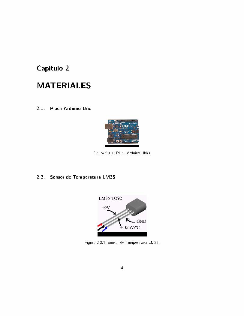
2.1. Placa Arduino Uno
Figura 2.1.1: Placa Arduino UNO.
2.2. Sensor de Temperatura LM35
Figura 2.2.1: Sensor de Temperatura LM35.
4
CAPÍTULO 2. MATERIALES 5
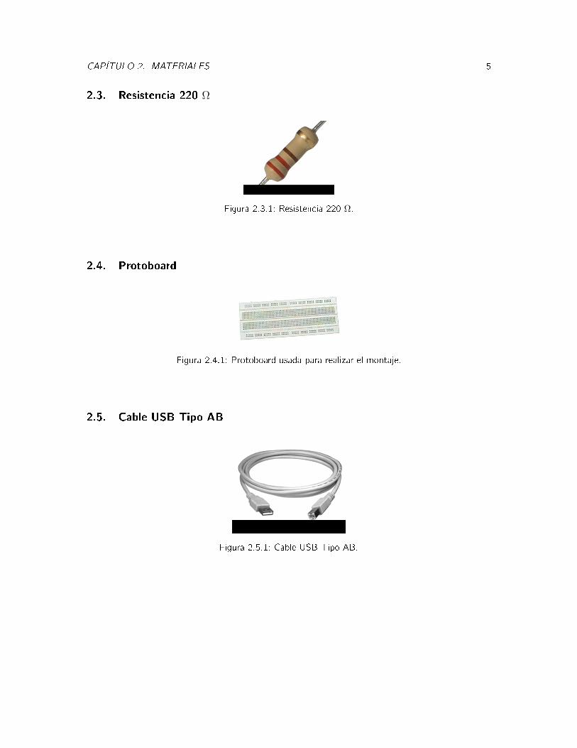
2.3. Resistencia 220 Ω
Figura 2.3.1: Resistencia 220 Ω.
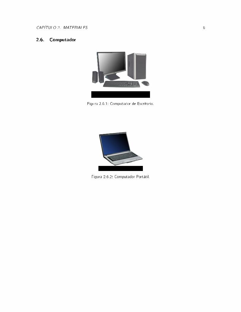
2.4. Protoboard
Figura 2.4.1: Protoboard usada para realizar el montaje.
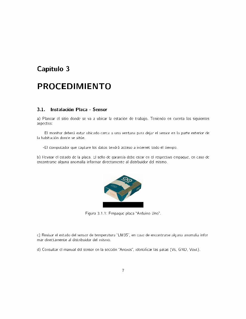
2.5. Cable USB Tipo AB
Figura 2.5.1: Cable USB Tipo AB.
CAPÍTULO 2. MATERIALES 6
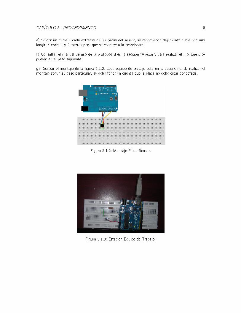
2.6. Computador
Figura 2.6.1: Computador de Escritorio.
Figura 2.6.2: Computador Portátil.
Capítulo 3
PROCEDIMIENTO
3.1. Instalación Placa - Sensor
a) Planear el sitio donde se va a ubicar la estación de trabajo. Teniendo en cuenta los siguientesaspectos:
-El monitor deberá estar ubicado cerca a una ventana para dejar el sensor en la parte exterior dela habitación donde se sitúe.
-El computador que capture los datos tendrá acceso a internet todo el tiempo.
b) Revisar el estado de la placa. El sello de garantía debe estar en el respectivo empaque, en caso deencontrarse alguna anomalía informar directamente al distrbuidor del mismo.
Figura 3.1.1: Empaque placa Arduino Uno.
c) Revisar el estado del sensor de temperatura LM35, en caso de encontrarse alguna anomalia infor-mar directamente al distribuidor del mismo.
d) Consultar el manual del sensor en la sección Anexos, identicar las patas (Vs, GND, Vout).
7
CAPÍTULO 3. PROCEDIMIENTO 8
e) Soldar un cable a cada extremo de las patas del sensor, se recomienda dejar cada cable con unalongitud entre 1 y 2 metros para que se conecte a la protoboard.
f) Consultar el manual de uso de la protoboard en la sección Anexos, para realizar el montaje pro-puesto en el paso siguiente.
g) Realizar el montaje de la gura 3.1.2, cada equipo de trabajo esta en la autonomía de realizar elmontaje según su caso particular, se debe tener en cuenta que la placa no debe estar conectada.
Figura 3.1.2: Montaje Placa-Sensor.
Figura 3.1.3: Estación Equipo de Trabajo.
CAPÍTULO 3. PROCEDIMIENTO 9
3.2. Comunicación Placa - PC
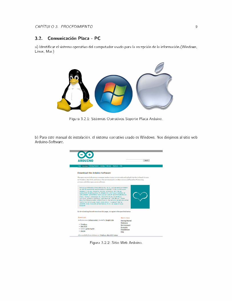
a) Identicar el sistema operativo del computador usado para la recepción de la información.(Windows,Linux, Mac)
Figura 3.2.1: Sistemas Operativos Soporte Placa Arduino.
b) Para este manual de instalación, el sistema operativo usado es Windows. Nos dirigimos al sitio webArduino-Software.
Figura 3.2.2: Sitio Web Arduino.
CAPÍTULO 3. PROCEDIMIENTO 10
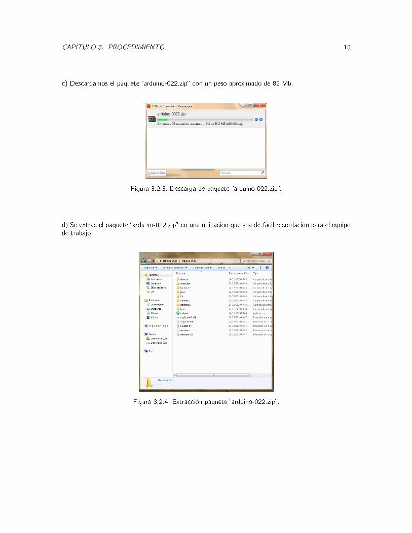
c) Descargamos el paquete arduino-022.zip con un peso aproximado de 85 Mb.
Figura 3.2.3: Descarga de paquete arduino-022.zip.
d) Se extrae el paquete arduino-022.zip en una ubicación que sea de fácil recordación para el equipode trabajo.
Figura 3.2.4: Extracción paquete arduino-022.zip.
CAPÍTULO 3. PROCEDIMIENTO 11
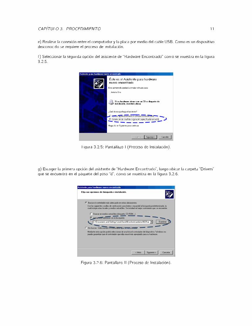
e) Realizar la conexión entre el computador y la placa por medio del cable USB. Como es un dispositivodesconocido se requiere el proceso de instalación.
f) Seleccionar la segunda opción del asistente de Hardware Encontrado como se muestra en la gura3.2.5.
Figura 3.2.5: Pantallazo I (Proceso de Instalación).
g) Escoger la primera opción del asistente de Hardware Encontrado, luego ubicar la carpeta Driversque se encuentra en el paquete del paso d, como se muestra en la gura 3.2.6.
Figura 3.2.6: Pantallazo II (Proceso de Instalación).
CAPÍTULO 3. PROCEDIMIENTO 12
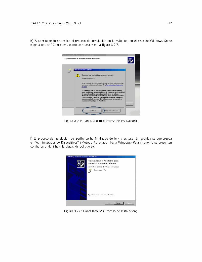
h) A continuación se realiza el proceso de instalación en la máquina, en el caso de Windows Xp seelige la opción Continuar, como se muestra en la gura 3.2.7.
Figura 3.2.7: Pantallazo III (Proceso de Instalación).
i) El proceso de instalación del periférico ha nalizado de forma exitosa. En seguida se compruebaen Administrador de Dispositivos (Método Abreviado=Tecla Windows+Pausa) que no se presentenconictos e identicar la ubicación del puerto.
Figura 3.2.8: Pantallazo IV (Proceso de Instalación).
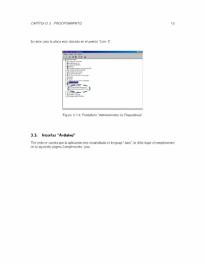
CAPÍTULO 3. PROCEDIMIENTO 13
En este caso la placa esta ubicada en el puerto Com 3.
Figura 3.2.9: Pantallazo Administrador de Dispositivos
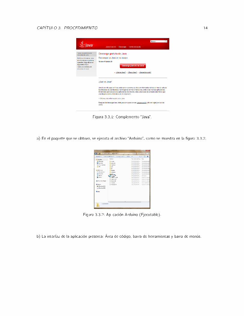
3.3. Interfaz Arduino
Teniendo en cuenta que la aplicación esta desarrollada en lenguaje Java, se debe bajar el complementoen la siguiente página.Complemento Java.
CAPÍTULO 3. PROCEDIMIENTO 14
Figura 3.3.1: Complemento Java.
a) En el paquete que se obtuvo, se ejecuta el archivo Arduino, como se muestra en la gura 3.3.2.
Figura 3.3.2: Aplicación Arduino (Ejecutable).
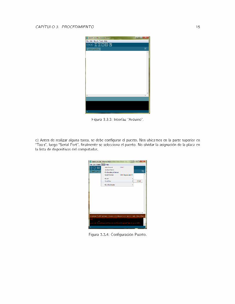
b) La interfaz de la aplicación presenta: Área de código, barra de herramientas y barra de menús.
CAPÍTULO 3. PROCEDIMIENTO 15
Figura 3.3.3: Interfaz Arduino.
c) Antes de realizar alguna tarea, se debe congurar el puerto. Nos ubicamos en la parte superior enTools, luego Serial Port, nalmente se selecciona el puerto. No olvidar la asignación de la placa enla lista de dispositivos del computador.
Figura 3.3.4: Conguración Puerto.
CAPÍTULO 3. PROCEDIMIENTO 16
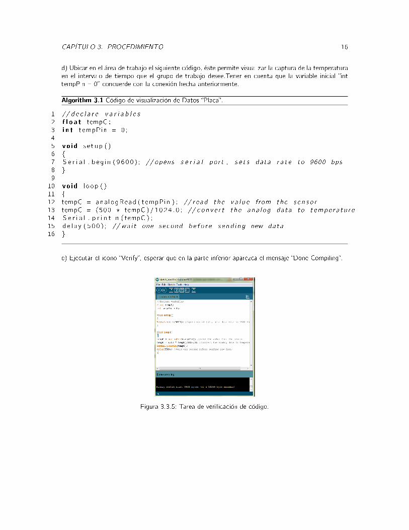
d) Ubicar en el área de trabajo el siguiente código, éste permite visualizar la captura de la temperaturaen el intervalo de tiempo que el grupo de trabajo desee.Tener en cuenta que la variable inicial inttempPin = 0 concuerde con la conexión hecha anteriormente.
Algorithm 3.1 Código de visualización de Datos Placa.
1 // d e c l a r e v a r i a b l e s2 f l o a t tempC ;3 i n t tempPin = 0 ;45 vo id s e t up ( )6 7 S e r i a l . b e g i n ( 9 600 ) ; // opens s e r i a l po r t , s e t s data r a t e to 9600 bps8 9
10 vo id l o o p ( )11 12 tempC = ana logRead ( tempPin ) ; // r ead the v a l u e from the s e n s o r13 tempC = (500 tempC )/1024 . 0 ; // c o n v e r t the ana l o g data to t empe r a t u r e14 S e r i a l . p r i n t l n ( tempC ) ;15 d e l a y ( 5 0 0 ) ; // wa i t one second b e f o r e s e n d i n g new data16
e) Ejecutar el icono Verify, esperar que en la parte inferior aparezca el mensaje Done Compiling.
Figura 3.3.5: Tarea de vericación de código.
CAPÍTULO 3. PROCEDIMIENTO 17
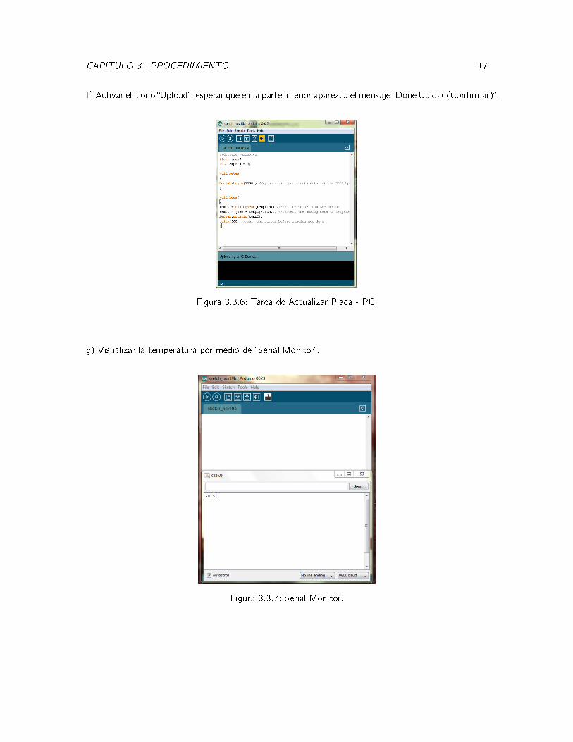
f) Activar el icono Upload, esperar que en la parte inferior aparezca el mensaje Done Upload(Conrmar).
Figura 3.3.6: Tarea de Actualizar Placa - PC.
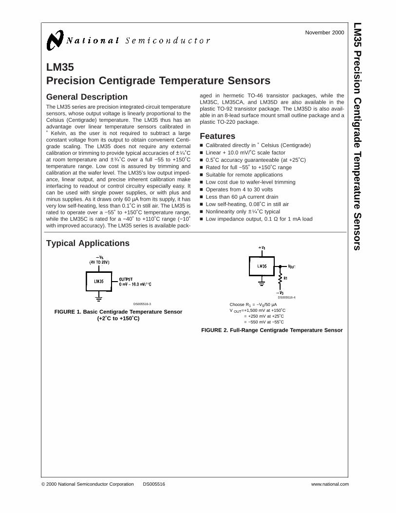
g) Visualizar la temperatura por medio de Serial Monitor.
Figura 3.3.7: Serial Monitor.

CAPÍTULO 3. PROCEDIMIENTO 18
3.4. Envio Datos - Servidor

Capítulo 4
Anexos
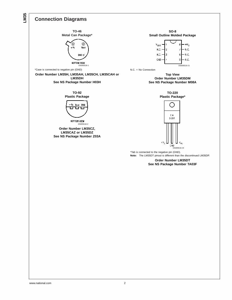
4.1. Documento Ocial Sensor LM35
19
LM35Precision Centigrade Temperature SensorsGeneral DescriptionThe LM35 series are precision integrated-circuit temperaturesensors, whose output voltage is linearly proportional to theCelsius (Centigrade) temperature. The LM35 thus has anadvantage over linear temperature sensors calibrated in˚ Kelvin, as the user is not required to subtract a largeconstant voltage from its output to obtain convenient Centi-grade scaling. The LM35 does not require any externalcalibration or trimming to provide typical accuracies of ±1⁄4˚Cat room temperature and ±3⁄4˚C over a full −55 to +150˚Ctemperature range. Low cost is assured by trimming andcalibration at the wafer level. The LM35’s low output imped-ance, linear output, and precise inherent calibration makeinterfacing to readout or control circuitry especially easy. Itcan be used with single power supplies, or with plus andminus supplies. As it draws only 60 µA from its supply, it hasvery low self-heating, less than 0.1˚C in still air. The LM35 israted to operate over a −55˚ to +150˚C temperature range,while the LM35C is rated for a −40˚ to +110˚C range (−10˚with improved accuracy). The LM35 series is available pack-
aged in hermetic TO-46 transistor packages, while theLM35C, LM35CA, and LM35D are also available in theplastic TO-92 transistor package. The LM35D is also avail-able in an 8-lead surface mount small outline package and aplastic TO-220 package.
Featuresn Calibrated directly in ˚ Celsius (Centigrade)n Linear + 10.0 mV/˚C scale factorn 0.5˚C accuracy guaranteeable (at +25˚C)n Rated for full −55˚ to +150˚C rangen Suitable for remote applicationsn Low cost due to wafer-level trimmingn Operates from 4 to 30 voltsn Less than 60 µA current drainn Low self-heating, 0.08˚C in still airn Nonlinearity only ±1⁄4˚C typicaln Low impedance output, 0.1 Ω for 1 mA load
Typical Applications
DS005516-3
FIGURE 1. Basic Centigrade Temperature Sensor(+2˚C to +150˚C)
DS005516-4
Choose R1 = −VS/50 µAV OUT=+1,500 mV at +150˚C
= +250 mV at +25˚C= −550 mV at −55˚C
FIGURE 2. Full-Range Centigrade Temperature Sensor
November 2000LM
35P
recisionC
entigradeTem
peratureS
ensors
© 2000 National Semiconductor Corporation DS005516 www.national.com
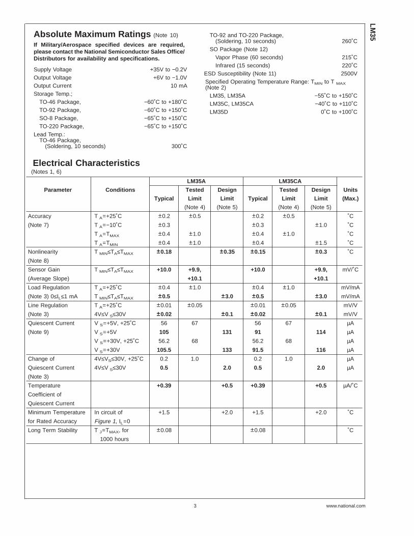
Connection Diagrams
TO-46Metal Can Package*
DS005516-1
*Case is connected to negative pin (GND)
Order Number LM35H, LM35AH, LM35CH, LM35CAH orLM35DH
See NS Package Number H03H
TO-92Plastic Package
DS005516-2
Order Number LM35CZ,LM35CAZ or LM35DZ
See NS Package Number Z03A
SO-8Small Outline Molded Package
DS005516-21
N.C. = No Connection
Top ViewOrder Number LM35DM
See NS Package Number M08A
TO-220Plastic Package*
DS005516-24
*Tab is connected to the negative pin (GND).Note: The LM35DT pinout is different than the discontinued LM35DP.
Order Number LM35DTSee NS Package Number TA03F
LM35
www.national.com 2
Absolute Maximum Ratings (Note 10)
If Military/Aerospace specified devices are required,please contact the National Semiconductor Sales Office/Distributors for availability and specifications.
Supply Voltage +35V to −0.2VOutput Voltage +6V to −1.0VOutput Current 10 mAStorage Temp.;
TO-46 Package, −60˚C to +180˚CTO-92 Package, −60˚C to +150˚CSO-8 Package, −65˚C to +150˚CTO-220 Package, −65˚C to +150˚C
Lead Temp.:TO-46 Package,
(Soldering, 10 seconds) 300˚C
TO-92 and TO-220 Package,(Soldering, 10 seconds) 260˚C
SO Package (Note 12)Vapor Phase (60 seconds) 215˚CInfrared (15 seconds) 220˚C
ESD Susceptibility (Note 11) 2500VSpecified Operating Temperature Range: TMIN to T MAX(Note 2)
LM35, LM35A −55˚C to +150˚CLM35C, LM35CA −40˚C to +110˚CLM35D 0˚C to +100˚C
Electrical Characteristics(Notes 1, 6)
LM35A LM35CA
Parameter Conditions Tested Design Tested Design Units
Typical Limit Limit Typical Limit Limit (Max.)
(Note 4) (Note 5) (Note 4) (Note 5)
Accuracy T A=+25˚C ±0.2 ±0.5 ±0.2 ±0.5 ˚C
(Note 7) T A=−10˚C ±0.3 ±0.3 ±1.0 ˚C
T A=TMAX ±0.4 ±1.0 ±0.4 ±1.0 ˚C
T A=TMIN ±0.4 ±1.0 ±0.4 ±1.5 ˚C
Nonlinearity T MIN≤TA≤TMAX ±0.18 ±0.35 ±0.15 ±0.3 ˚C
(Note 8)
Sensor Gain T MIN≤TA≤TMAX +10.0 +9.9, +10.0 +9.9, mV/˚C
(Average Slope) +10.1 +10.1
Load Regulation T A=+25˚C ±0.4 ±1.0 ±0.4 ±1.0 mV/mA
(Note 3) 0≤IL≤1 mA T MIN≤TA≤TMAX ±0.5 ±3.0 ±0.5 ±3.0 mV/mA
Line Regulation T A=+25˚C ±0.01 ±0.05 ±0.01 ±0.05 mV/V
(Note 3) 4V≤V S≤30V ±0.02 ±0.1 ±0.02 ±0.1 mV/V
Quiescent Current V S=+5V, +25˚C 56 67 56 67 µA
(Note 9) V S=+5V 105 131 91 114 µA
V S=+30V, +25˚C 56.2 68 56.2 68 µA
V S=+30V 105.5 133 91.5 116 µA
Change of 4V≤VS≤30V, +25˚C 0.2 1.0 0.2 1.0 µA
Quiescent Current 4V≤V S≤30V 0.5 2.0 0.5 2.0 µA
(Note 3)
Temperature +0.39 +0.5 +0.39 +0.5 µA/˚C
Coefficient of
Quiescent Current
Minimum Temperature In circuit of +1.5 +2.0 +1.5 +2.0 ˚C
for Rated Accuracy Figure 1, IL=0
Long Term Stability T J=TMAX, for ±0.08 ±0.08 ˚C
1000 hours
LM35
www.national.com3
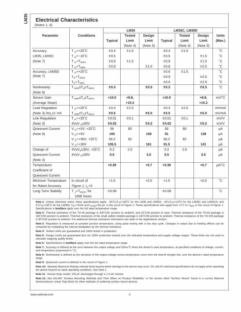
Electrical Characteristics(Notes 1, 6)
LM35 LM35C, LM35D
Parameter Conditions Tested Design Tested Design Units
Typical Limit Limit Typical Limit Limit (Max.)
(Note 4) (Note 5) (Note 4) (Note 5)
Accuracy, T A=+25˚C ±0.4 ±1.0 ±0.4 ±1.0 ˚C
LM35, LM35C T A=−10˚C ±0.5 ±0.5 ±1.5 ˚C
(Note 7) T A=TMAX ±0.8 ±1.5 ±0.8 ±1.5 ˚C
T A=TMIN ±0.8 ±1.5 ±0.8 ±2.0 ˚C
Accuracy, LM35D(Note 7)
T A=+25˚C ±0.6 ±1.5 ˚C
TA=TMAX ±0.9 ±2.0 ˚C
TA=TMIN ±0.9 ±2.0 ˚C
Nonlinearity T MIN≤TA≤TMAX ±0.3 ±0.5 ±0.2 ±0.5 ˚C
(Note 8)
Sensor Gain T MIN≤TA≤TMAX +10.0 +9.8, +10.0 +9.8, mV/˚C
(Average Slope) +10.2 +10.2
Load Regulation T A=+25˚C ±0.4 ±2.0 ±0.4 ±2.0 mV/mA
(Note 3) 0≤IL≤1 mA T MIN≤TA≤TMAX ±0.5 ±5.0 ±0.5 ±5.0 mV/mA
Line Regulation T A=+25˚C ±0.01 ±0.1 ±0.01 ±0.1 mV/V
(Note 3) 4V≤V S≤30V ±0.02 ±0.2 ±0.02 ±0.2 mV/V
Quiescent Current V S=+5V, +25˚C 56 80 56 80 µA
(Note 9) V S=+5V 105 158 91 138 µA
V S=+30V, +25˚C 56.2 82 56.2 82 µA
V S=+30V 105.5 161 91.5 141 µA
Change of 4V≤VS≤30V, +25˚C 0.2 2.0 0.2 2.0 µA
Quiescent Current 4V≤V S≤30V 0.5 3.0 0.5 3.0 µA
(Note 3)
Temperature +0.39 +0.7 +0.39 +0.7 µA/˚C
Coefficient of
Quiescent Current
Minimum Temperature In circuit of +1.5 +2.0 +1.5 +2.0 ˚C
for Rated Accuracy Figure 1, IL=0
Long Term Stability T J=TMAX, for ±0.08 ±0.08 ˚C
1000 hours
Note 1: Unless otherwise noted, these specifications apply: −55˚C≤TJ≤+150˚C for the LM35 and LM35A; −40˚≤TJ≤+110˚C for the LM35C and LM35CA; and0˚≤TJ≤+100˚C for the LM35D. VS=+5Vdc and ILOAD=50 µA, in the circuit of Figure 2. These specifications also apply from +2˚C to TMAX in the circuit of Figure 1.Specifications in boldface apply over the full rated temperature range.
Note 2: Thermal resistance of the TO-46 package is 400˚C/W, junction to ambient, and 24˚C/W junction to case. Thermal resistance of the TO-92 package is180˚C/W junction to ambient. Thermal resistance of the small outline molded package is 220˚C/W junction to ambient. Thermal resistance of the TO-220 packageis 90˚C/W junction to ambient. For additional thermal resistance information see table in the Applications section.
Note 3: Regulation is measured at constant junction temperature, using pulse testing with a low duty cycle. Changes in output due to heating effects can becomputed by multiplying the internal dissipation by the thermal resistance.
Note 4: Tested Limits are guaranteed and 100% tested in production.
Note 5: Design Limits are guaranteed (but not 100% production tested) over the indicated temperature and supply voltage ranges. These limits are not used tocalculate outgoing quality levels.
Note 6: Specifications in boldface apply over the full rated temperature range.
Note 7: Accuracy is defined as the error between the output voltage and 10mv/˚C times the device’s case temperature, at specified conditions of voltage, current,and temperature (expressed in ˚C).
Note 8: Nonlinearity is defined as the deviation of the output-voltage-versus-temperature curve from the best-fit straight line, over the device’s rated temperaturerange.
Note 9: Quiescent current is defined in the circuit of Figure 1.
Note 10: Absolute Maximum Ratings indicate limits beyond which damage to the device may occur. DC and AC electrical specifications do not apply when operatingthe device beyond its rated operating conditions. See Note 1.
Note 11: Human body model, 100 pF discharged through a 1.5 kΩ resistor.
Note 12: See AN-450 “Surface Mounting Methods and Their Effect on Product Reliability” or the section titled “Surface Mount” found in a current NationalSemiconductor Linear Data Book for other methods of soldering surface mount devices.
LM35
www.national.com 4
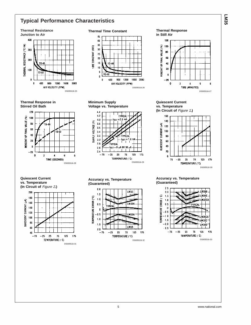
Typical Performance Characteristics
Thermal ResistanceJunction to Air
DS005516-25
Thermal Time Constant
DS005516-26
Thermal Responsein Still Air
DS005516-27
Thermal Response inStirred Oil Bath
DS005516-28
Minimum SupplyVoltage vs. Temperature
DS005516-29
Quiescent Currentvs. Temperature(In Circuit of Figure 1.)
DS005516-30
Quiescent Currentvs. Temperature(In Circuit of Figure 2.)
DS005516-31
Accuracy vs. Temperature(Guaranteed)
DS005516-32
Accuracy vs. Temperature(Guaranteed)
DS005516-33
LM35
www.national.com5
Typical Performance Characteristics (Continued)
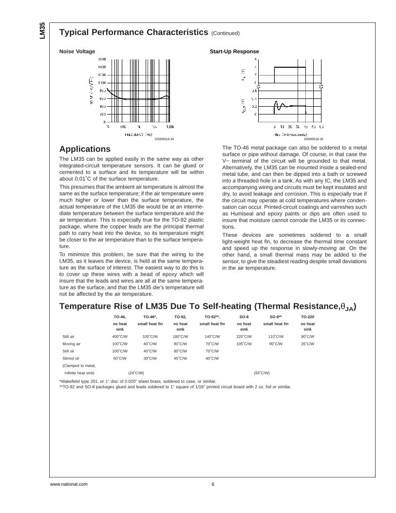
ApplicationsThe LM35 can be applied easily in the same way as otherintegrated-circuit temperature sensors. It can be glued orcemented to a surface and its temperature will be withinabout 0.01˚C of the surface temperature.
This presumes that the ambient air temperature is almost thesame as the surface temperature; if the air temperature weremuch higher or lower than the surface temperature, theactual temperature of the LM35 die would be at an interme-diate temperature between the surface temperature and theair temperature. This is expecially true for the TO-92 plasticpackage, where the copper leads are the principal thermalpath to carry heat into the device, so its temperature mightbe closer to the air temperature than to the surface tempera-ture.
To minimize this problem, be sure that the wiring to theLM35, as it leaves the device, is held at the same tempera-ture as the surface of interest. The easiest way to do this isto cover up these wires with a bead of epoxy which willinsure that the leads and wires are all at the same tempera-ture as the surface, and that the LM35 die’s temperature willnot be affected by the air temperature.
The TO-46 metal package can also be soldered to a metalsurface or pipe without damage. Of course, in that case theV− terminal of the circuit will be grounded to that metal.Alternatively, the LM35 can be mounted inside a sealed-endmetal tube, and can then be dipped into a bath or screwedinto a threaded hole in a tank. As with any IC, the LM35 andaccompanying wiring and circuits must be kept insulated anddry, to avoid leakage and corrosion. This is especially true ifthe circuit may operate at cold temperatures where conden-sation can occur. Printed-circuit coatings and varnishes suchas Humiseal and epoxy paints or dips are often used toinsure that moisture cannot corrode the LM35 or its connec-tions.
These devices are sometimes soldered to a smalllight-weight heat fin, to decrease the thermal time constantand speed up the response in slowly-moving air. On theother hand, a small thermal mass may be added to thesensor, to give the steadiest reading despite small deviationsin the air temperature.
Temperature Rise of LM35 Due To Self-heating (Thermal Resistance, θJA)TO-46, TO-46*, TO-92, TO-92**, SO-8 SO-8** TO-220
no heatsink
small heat fin no heatsink
small heat fin no heatsink
small heat fin no heatsink
Still air 400˚C/W 100˚C/W 180˚C/W 140˚C/W 220˚C/W 110˚C/W 90˚C/W
Moving air 100˚C/W 40˚C/W 90˚C/W 70˚C/W 105˚C/W 90˚C/W 26˚C/W
Still oil 100˚C/W 40˚C/W 90˚C/W 70˚C/W
Stirred oil 50˚C/W 30˚C/W 45˚C/W 40˚C/W
(Clamped to metal,
Infinite heat sink) (24˚C/W) (55˚C/W)
*Wakefield type 201, or 1" disc of 0.020" sheet brass, soldered to case, or similar.**TO-92 and SO-8 packages glued and leads soldered to 1" square of 1/16" printed circuit board with 2 oz. foil or similar.
Noise Voltage
DS005516-34
Start-Up Response
DS005516-35
LM35
www.national.com 6
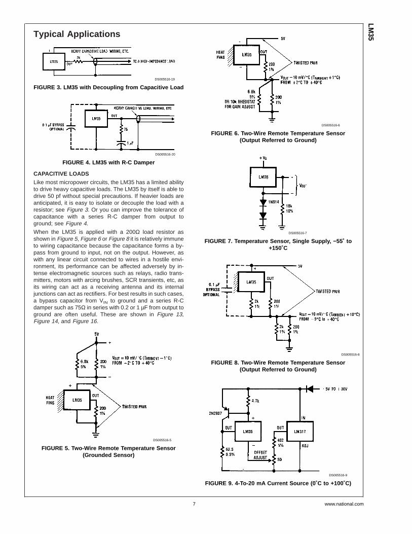
Typical Applications
CAPACITIVE LOADS
Like most micropower circuits, the LM35 has a limited abilityto drive heavy capacitive loads. The LM35 by itself is able todrive 50 pf without special precautions. If heavier loads areanticipated, it is easy to isolate or decouple the load with aresistor; see Figure 3. Or you can improve the tolerance ofcapacitance with a series R-C damper from output toground; see Figure 4.
When the LM35 is applied with a 200Ω load resistor asshown in Figure 5, Figure 6 or Figure 8 it is relatively immuneto wiring capacitance because the capacitance forms a by-pass from ground to input, not on the output. However, aswith any linear circuit connected to wires in a hostile envi-ronment, its performance can be affected adversely by in-tense electromagnetic sources such as relays, radio trans-mitters, motors with arcing brushes, SCR transients, etc, asits wiring can act as a receiving antenna and its internaljunctions can act as rectifiers. For best results in such cases,a bypass capacitor from VIN to ground and a series R-Cdamper such as 75Ω in series with 0.2 or 1 µF from output toground are often useful. These are shown in Figure 13,Figure 14, and Figure 16.
DS005516-19
FIGURE 3. LM35 with Decoupling from Capacitive Load
DS005516-20
FIGURE 4. LM35 with R-C Damper
DS005516-5
FIGURE 5. Two-Wire Remote Temperature Sensor(Grounded Sensor)
DS005516-6
FIGURE 6. Two-Wire Remote Temperature Sensor(Output Referred to Ground)
DS005516-7
FIGURE 7. Temperature Sensor, Single Supply, −55˚ to+150˚C
DS005516-8
FIGURE 8. Two-Wire Remote Temperature Sensor(Output Referred to Ground)
DS005516-9
FIGURE 9. 4-To-20 mA Current Source (0˚C to +100˚C)
LM35
www.national.com7
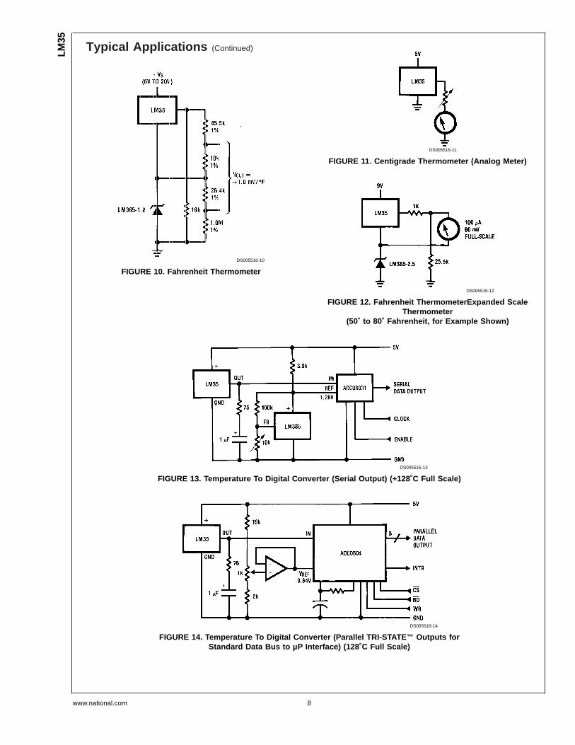
Typical Applications (Continued)
DS005516-10
FIGURE 10. Fahrenheit Thermometer
DS005516-11
FIGURE 11. Centigrade Thermometer (Analog Meter)
DS005516-12
FIGURE 12. Fahrenheit ThermometerExpanded ScaleThermometer
(50˚ to 80˚ Fahrenheit, for Example Shown)
DS005516-13
FIGURE 13. Temperature To Digital Converter (Serial Output) (+128˚C Full Scale)
DS005516-14
FIGURE 14. Temperature To Digital Converter (Parallel TRI-STATE ™ Outputs forStandard Data Bus to µP Interface) (128˚C Full Scale)
LM35
www.national.com 8
Typical Applications (Continued)
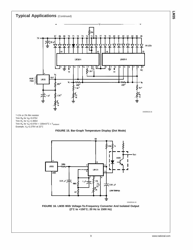
DS005516-16
*=1% or 2% film resistorTrim RB for VB=3.075VTrim RC for VC=1.955VTrim RA for VA=0.075V + 100mV/˚C x TambientExample, VA=2.275V at 22˚C
FIGURE 15. Bar-Graph Temperature Display (Dot Mode)
DS005516-15
FIGURE 16. LM35 With Voltage-To-Frequency Converter And Isolated Output(2˚C to +150˚C; 20 Hz to 1500 Hz)
LM35
www.national.com9
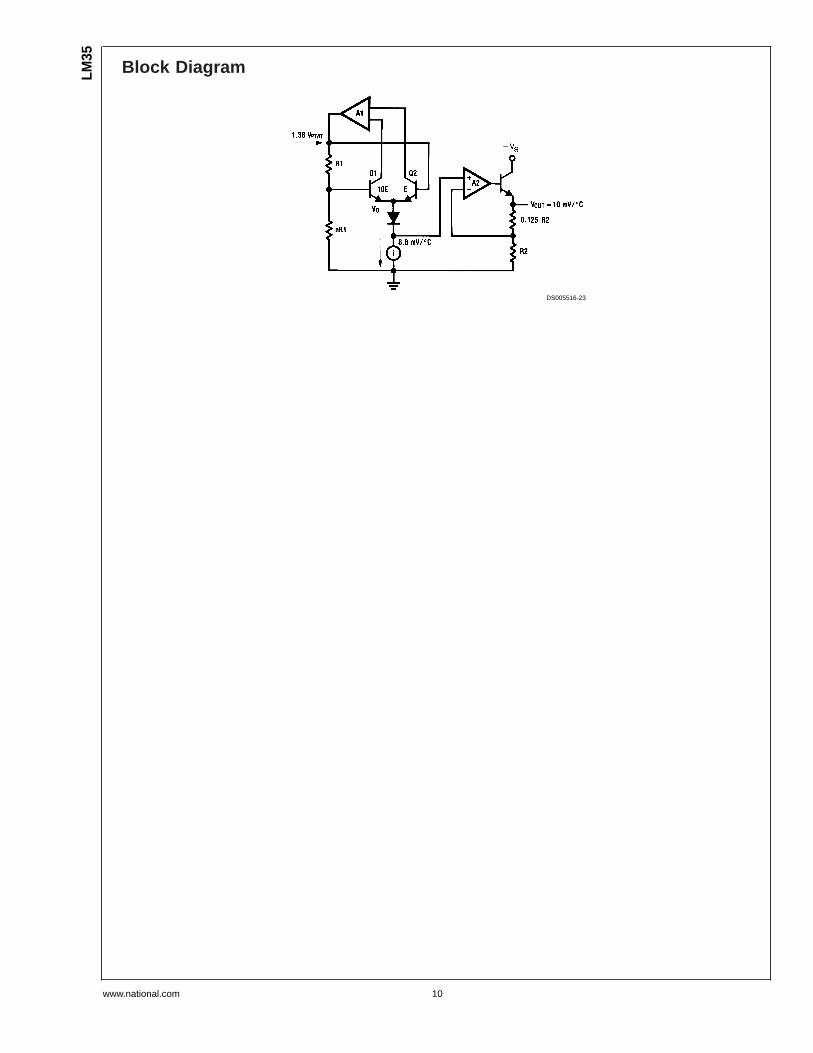
Block Diagram
DS005516-23
LM35
www.national.com 10
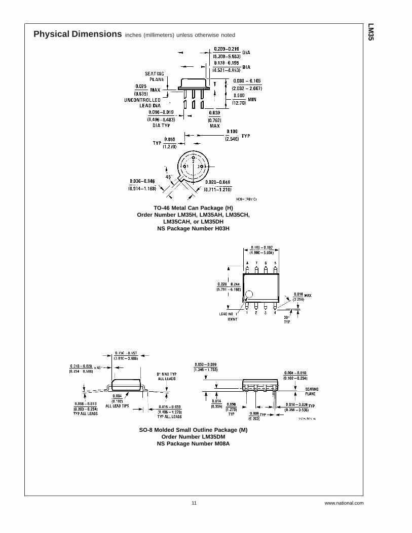
Physical Dimensions inches (millimeters) unless otherwise noted
TO-46 Metal Can Package (H)Order Number LM35H, LM35AH, LM35CH,
LM35CAH, or LM35DHNS Package Number H03H
SO-8 Molded Small Outline Package (M)Order Number LM35DM
NS Package Number M08A
LM35
www.national.com11
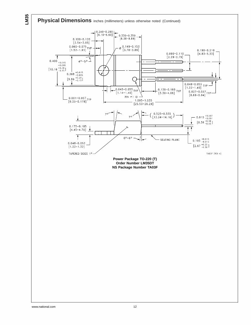
Physical Dimensions inches (millimeters) unless otherwise noted (Continued)
Power Package TO-220 (T)Order Number LM35DT
NS Package Number TA03F
LM35
www.national.com 12
Physical Dimensions inches (millimeters) unless otherwise noted (Continued)
LIFE SUPPORT POLICY
NATIONAL’S PRODUCTS ARE NOT AUTHORIZED FOR USE AS CRITICAL COMPONENTS IN LIFE SUPPORTDEVICES OR SYSTEMS WITHOUT THE EXPRESS WRITTEN APPROVAL OF THE PRESIDENT AND GENERALCOUNSEL OF NATIONAL SEMICONDUCTOR CORPORATION. As used herein:
1. Life support devices or systems are devices orsystems which, (a) are intended for surgical implantinto the body, or (b) support or sustain life, andwhose failure to perform when properly used inaccordance with instructions for use provided in thelabeling, can be reasonably expected to result in asignificant injury to the user.
2. A critical component is any component of a lifesupport device or system whose failure to performcan be reasonably expected to cause the failure ofthe life support device or system, or to affect itssafety or effectiveness.
National SemiconductorCorporationAmericasTel: 1-800-272-9959Fax: 1-800-737-7018Email: [email protected]
National SemiconductorEurope
Fax: +49 (0) 180-530 85 86Email: [email protected]
Deutsch Tel: +49 (0) 69 9508 6208English Tel: +44 (0) 870 24 0 2171Français Tel: +33 (0) 1 41 91 8790
National SemiconductorAsia Pacific CustomerResponse GroupTel: 65-2544466Fax: 65-2504466Email: [email protected]
National SemiconductorJapan Ltd.Tel: 81-3-5639-7560Fax: 81-3-5639-7507
www.national.com
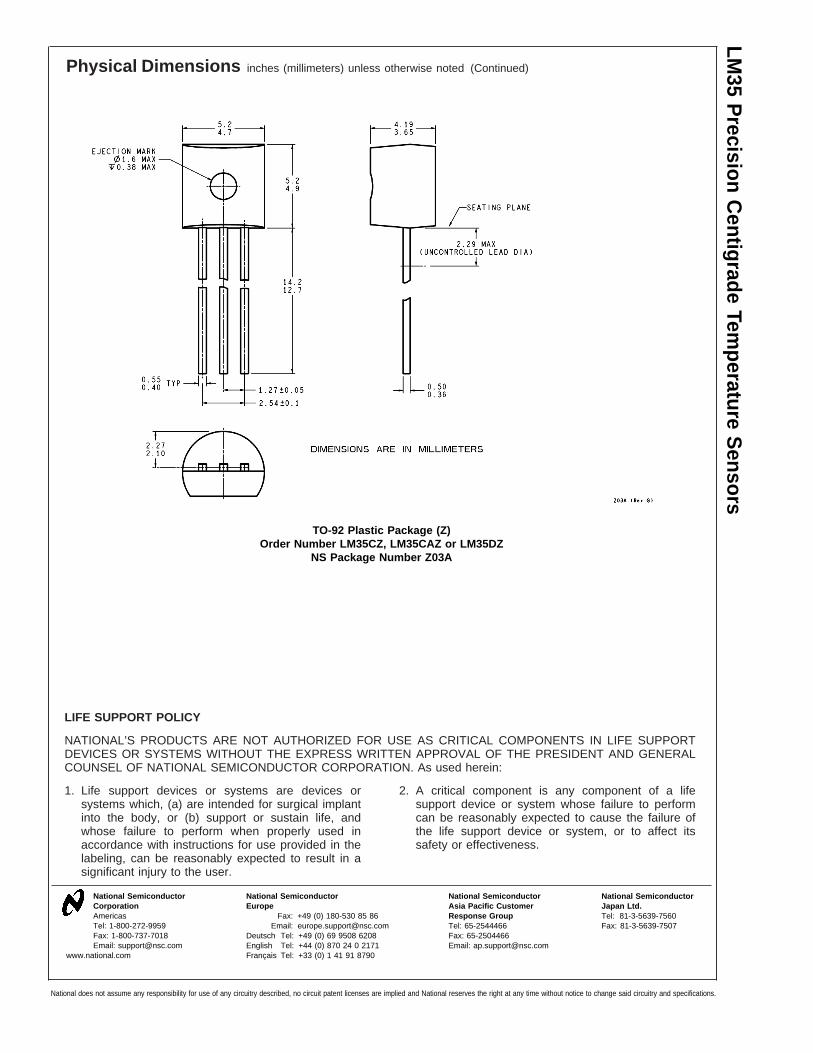
TO-92 Plastic Package (Z)Order Number LM35CZ, LM35CAZ or LM35DZ
NS Package Number Z03A
LM35
Precision
Centigrade
Temperature
Sensors
National does not assume any responsibility for use of any circuitry described, no circuit patent licenses are implied and National reserves the right at any time without notice to change said circuitry and specifications.

CAPÍTULO 4. ANEXOS 33
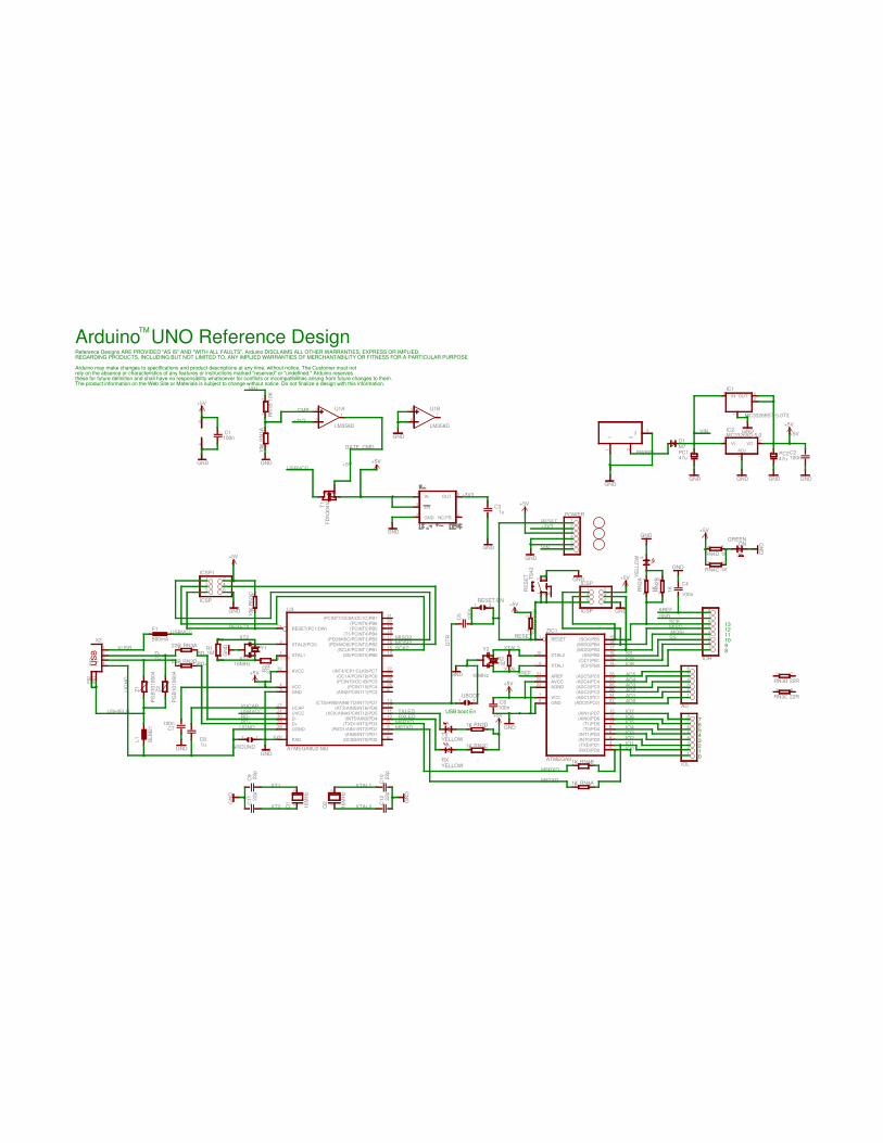
4.2. Documento Ocial Placa Arduino Uno
ATMEGA8
ICSP
+5V
GND+5V
+5V
GND
GND
GND
+5V
GND
100n
GND
47u 47u
GND GND
GND
GND
GREEN
GN
D
+5V
YELLOW
YELLOW
M7
GNDMC33269D-5.0
MC33269ST-5.0T3
100n
GND
500mA
+5V
+5V
100n
GND
YE
LLO
W
GND
FDN
304V
+5VLM358D LM358D
GNDGND
+5V
100n
+5V
ATMEGA8U2-MU
GND
100n
ICSP
+5V
GND
GND
16MHz
16MHz
GN
D
PG
B10
1060
4
PG
B10
1060
4
BLM
21
1M
1K 1K
1K
1K
GND
10K
10K
10K
10K
100n
1u
1K
1K
1K
1K
22R
22R
22R
22R
1u
1M
16M
Hz
16M
Hz
TS42
22p
22p
22p
22p
GN
D
GN
D
GND
27R
(ADC5)PC5 28
(ADC4)PC4 27
(ADC3)PC3 26
(ADC2)PC2 25
(ADC1)PC1 24
(ADC0)PC0) 23
(SCK)PB5 19
(MISO)PB4 18
(MOSI)PB3 17
(SS)PB2 16
(OC1)PB1 15
(ICP)PB0 14
(AIN1)PD7 13
(AIN0)PD6 12
(T1)PD5 11
(T0)PD4 6
(INT1)PD3 5
(INT0)PD2 4
(TXD)PD1 3
(RXD)PD0 2
GND8VCC7
AVCC20AREF21
XTAL19
XTAL210
RESET1
AGND22
ZIC1
1 23 45 6
ICSP
12345678
IOL
12345678
IOH
123456
AD
C2PC1 PC2
ON
RX
TX
D1
11
22
3 3
1234P
$1P
$1P
$2P
$2
X2
VI3
1
VO 2
IC2
ADJ
1
IN3 OUT 42
IC1
123456
POWER
C4
F1
C7
L
T1
2
31
U1A
6
57
U1B
84
C1
(PCINT9/OC1B)PC5 25
(PCINT10)PC4 26
(INT4/ICP1/CLK0)PC7 22
(OC1A/PCINT8)PC6 23
(AIN2/PCINT11)PC2 5
(PCINT5)PB5 19
(T1/PCINT4)PB4 18
(PD0/MISO/PCINT3)PB3 17
(PDI/MOSI/PCINT2)PB2 16
(SCLK/PCINT1)PB1 15
(SS/PCINT0)PB0 14
(CTS/HWB/AIN6/TO/INT7)PD7 13
(RTS/AIN5/INT6)PD6 12
(XCK/AIN4/PCINT12)PD5 11
(INT5/AIN3)PD4 10
(TXD1/INT3)PD3 9
(RXD1/AIN1/INT2)PD2 8
(AIN0/INT1)PD1 7
(OC0B/INT0)PD0 6
GND3VCC4
AVCC32
UVCC31
XTAL11
XTAL2(PC0)2
RESET(PC1/DW)24
UGND28
U3
PADEXP
UCAP27
D-30
D+29
(PCINT6)PB6 20(PCINT7/OC0A/OC1C)PB7 21 C
5
1 23 45 6
ICSP1
Y2Y1
21UBOOT
Z1 Z2
2 1
GROUND
L1
21RESET-EN
R2
18
RN
2A
27
RN
2B
36 RN2C
45 RN2D
18
RN
1A2
7
RN
1B
36
RN
1C
45
RN
1D
C6
C8
18 RN4A
27 RN4B
3 6
RN4C
4 5
RN4D
18 RN3A
2 7
RN3B
3 6
RN3C
45 RN3D
C3
R1
21Q1
21Q2
13 4
2
RE
SE
T
5
C10
C12
C9
C11
IN1
EN3
NC/FB 4
OUT 5
GND2
R3
+5V
+5V
GND
AREF
AREF
RESET
RESET
VIN
VIN
VIN
M8RXD
M8RXD
M8TXD
M8TXD
SCK
PWRIN
D-D+
+3V3
+3V3
+3V3
MISOMOSISS
SS
DTR
GATE_CMD
CMP
USBVCC
USBVCC
USBVCC
XTAL2
XTAL2
XTAL1
XTAL1
VUCAP
RD-
RD-
RD+
RD+
RESET2
MISO2MOSI2SCK2
USHIELD
UG
ND
UGND
XUSB
XT2
XT2
XT1
XT1
RXLEDTXLED
AD0AD1AD2AD3AD4AD5
IO2IO1IO0
IO3IO4IO5IO6IO7
IO8IO9XT1R
+ +
US
B
01234567
8910111213
Arduino UNO Reference Design
USB boot En
TM
Reference Designs ARE PROVIDED "AS IS" AND "WITH ALL FAULTS". Arduino DISCLAIMS ALL OTHER WARRANTIES, EXPRESS OR IMPLIED,
Arduino may make changes to specifications and product descriptions at any time, without notice. The Customer must not
REGARDING PRODUCTS, INCLUDING BUT NOT LIMITED TO, ANY IMPLIED WARRANTIES OF MERCHANTABILITY OR FITNESS FOR A PARTICULAR PURPOSE
rely on the absence or characteristics of any features or instructions marked "reserved" or "undefined." Arduino reservesthese for future definition and shall have no responsibility whatsoever for conflicts or incompatibilities arising from future changes to them.The product information on the Web Site or Materials is subject to change without notice. Do not finalize a design with this information.

CAPÍTULO 4. ANEXOS 35
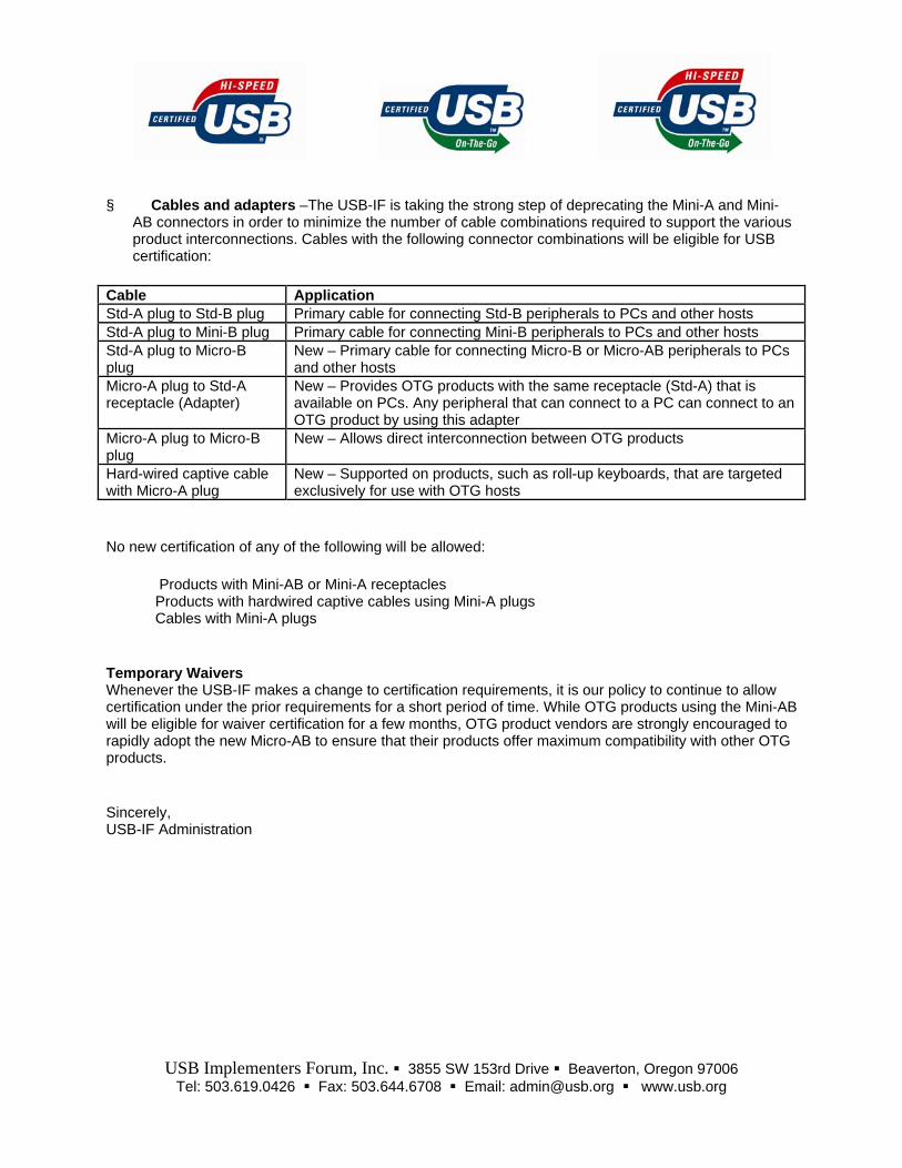
4.3. Documento Ocial Cable USB Tipo AB

USB Implementers Forum, Inc. 3855 SW 153rd Drive Beaverton, Oregon 97006 Tel: 503.619.0426 Fax: 503.644.6708 Email: [email protected] www.usb.org
May 23, 2007 To: USB Members and Vendors RE: Deprecation of the Mini-A and Mini-AB Connectors
Dear USB Developer,
With the recent introduction of the Micro-USB connectors, the USB-IF is taking the strong step to deprecate the Mini-A and Mini-AB connectors in order to minimize the number of cable combinations required to support the various product interconnections and minimize marketplace confusion. Based upon this, the USB-IF will no longer certify products that use the Mini-A and Mini-AB connectors nor products that use them. This change is effective immediately. Vendors of USB On-The-Go (OTG) products are directed to adopt the Micro-AB receptacle on all new OTG designs in lieu of the Mini-AB previously approved for this application. In addition, all Mini-A and Mini-AB connectors that are currently on the Integrators List will be removed. Specifications The USB Mini- and Micro-series connectors are defined in the following specifications:
§ Micro-USB Cables and Connectors Specification, Version 1.01 (http://www.usb.org/developers/docs/) – This newly released document defines the Micro-B receptacle (for USB peripherals), the Micro-AB receptacle (for OTG products) and the associated cables and plugs. The new Micro-series connectors offer a smaller footprint, improved insertion/extraction forces, passive latching and improved robustness.
§ On-The-Go Supplement to the USB 2.0 Specification, Version 1.3 – Previous versions of the OTG specification contained protocol and mechanical definitions, in this new version the mechanical section is removed. The Mini-A and Mini-AB cables and connectors previously defined in the OTG Supplement no longer have a place in any USB current specification.
§ Mini-B ECN to the USB 2.0 Specification – This document remains unchanged. It defines the Mini-B receptacle as well as associated plugs and cables.
Compliance Changes
§ Receptacles on non-OTG products – Portable non-OTG products may use either the Mini-B receptacle or the new Micro-B receptacle. The USB Standard-B receptacle is still recommended for products with adequate room.
§ Receptacles on OTG products – All products seeking OTG certification will be required to use one, and only one, Micro-AB receptacle and no other USB receptacles. (The Micro-AB receptacle is not approved on non-OTG products.) Products using the Mini-A and Mini-AB receptacles will no longer be eligible for USB-IF certification and are strongly discouraged.
USB Implementers Forum, Inc. 3855 SW 153rd Drive Beaverton, Oregon 97006 Tel: 503.619.0426 Fax: 503.644.6708 Email: [email protected] www.usb.org
§ Cables and adapters –The USB-IF is taking the strong step of deprecating the Mini-A and Mini-AB connectors in order to minimize the number of cable combinations required to support the various product interconnections. Cables with the following connector combinations will be eligible for USB certification:
Cable Application Std-A plug to Std-B plug Primary cable for connecting Std-B peripherals to PCs and other hosts Std-A plug to Mini-B plug Primary cable for connecting Mini-B peripherals to PCs and other hosts Std-A plug to Micro-B plug
New – Primary cable for connecting Micro-B or Micro-AB peripherals to PCs and other hosts
Micro-A plug to Std-A receptacle (Adapter)
New – Provides OTG products with the same receptacle (Std-A) that is available on PCs. Any peripheral that can connect to a PC can connect to an OTG product by using this adapter
Micro-A plug to Micro-B plug
New – Allows direct interconnection between OTG products
Hard-wired captive cable with Micro-A plug
New – Supported on products, such as roll-up keyboards, that are targeted exclusively for use with OTG hosts
No new certification of any of the following will be allowed:
Products with Mini-AB or Mini-A receptacles Products with hardwired captive cables using Mini-A plugs Cables with Mini-A plugs
Temporary Waivers Whenever the USB-IF makes a change to certification requirements, it is our policy to continue to allow certification under the prior requirements for a short period of time. While OTG products using the Mini-AB will be eligible for waiver certification for a few months, OTG product vendors are strongly encouraged to rapidly adopt the new Micro-AB to ensure that their products offer maximum compatibility with other OTG products.
Sincerely, USB-IF Administration

CAPÍTULO 4. ANEXOS 38
4.4. Documento Ocial Protoboard
El Protoboard
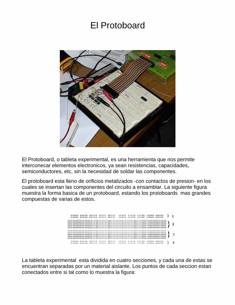
El Protoboard, o tableta experimental, es una herramienta que nos permiteinterconecar elementos electronicos, ya sean resistencias, capacidades,semiconductores, etc, sin la necesidad de soldar las componentes.
El protoboard esta lleno de orificios metalizados -con contactos de presion- en loscuales se insertan las componentes del circuito a ensamblar. La siguiente figuramuestra la forma basica de un protoboard, estando los protoboards mas grandescompuestas de varias de estos.
La tableta experimental esta dividida en cuatro secciones, y cada una de estas seencuentran separadas por un material aislante. Los puntos de cada seccion estanconectados entre si tal como lo muestra la figura:
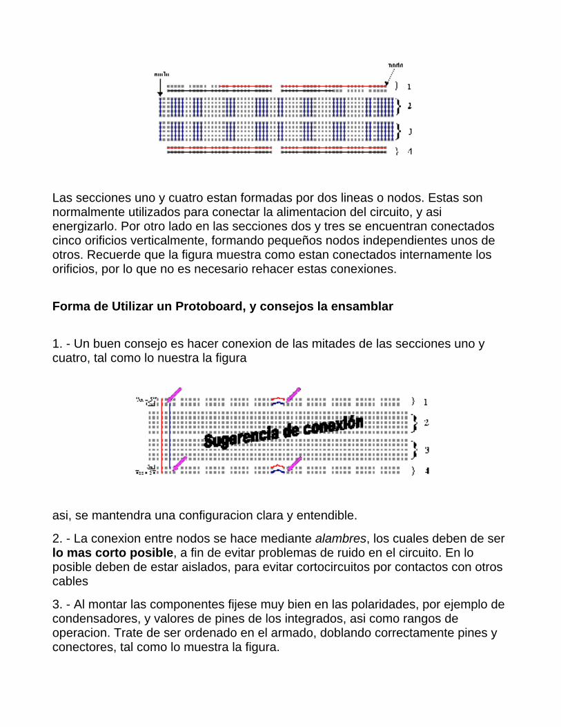
Las secciones uno y cuatro estan formadas por dos lineas o nodos. Estas sonnormalmente utilizados para conectar la alimentacion del circuito, y asienergizarlo. Por otro lado en las secciones dos y tres se encuentran conectadoscinco orificios verticalmente, formando pequeños nodos independientes unos deotros. Recuerde que la figura muestra como estan conectados internamente losorificios, por lo que no es necesario rehacer estas conexiones.
Forma de Utilizar un Protoboard, y consejos la ensamblar
1. - Un buen consejo es hacer conexion de las mitades de las secciones uno ycuatro, tal como lo nuestra la figura
asi, se mantendra una configuracion clara y entendible.
2. - La conexion entre nodos se hace mediante alambres, los cuales deben de serlo mas corto posible, a fin de evitar problemas de ruido en el circuito. En loposible deben de estar aislados, para evitar cortocircuitos por contactos con otroscables
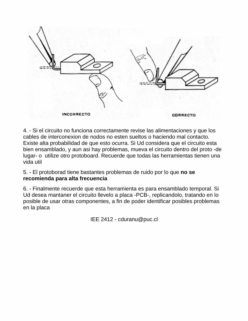
3. - Al montar las componentes fijese muy bien en las polaridades, por ejemplo decondensadores, y valores de pines de los integrados, asi como rangos deoperacion. Trate de ser ordenado en el armado, doblando correctamente pines yconectores, tal como lo muestra la figura.
4. - Si el circuito no funciona correctamente revise las alimentaciones y que loscables de interconexion de nodos no esten sueltos o haciendo mal contacto.Existe alta probabilidad de que esto ocurra. Si Ud considera que el circuito estabien ensamblado, y aun asi hay problemas, mueva el circuito dentro del proto -delugar- o utilize otro protoboard. Recuerde que todas las herramientas tienen unavida util
5. - El protoborad tiene bastantes problemas de ruido por lo que no serecomienda para alta frecuencia
6. - Finalmente recuerde que esta herramienta es para ensamblado temporal. SiUd desea mantaner el circuito llevelo a placa -PCB-, replicandolo, tratando en loposible de usar otras componentes, a fin de poder identificar posibles problemasen la placa
IEE 2412 - [email protected]
Índice de guras
2.1.1.Placa Arduino UNO. . . . . . . . . . . . . . . . . . . . . . . . . . . . . . . . . . . . . . 42.2.1.Sensor de Temperatura LM35. . . . . . . . . . . . . . . . . . . . . . . . . . . . . . . . . 42.3.1.Resistencia 220 Ω. . . . . . . . . . . . . . . . . . . . . . . . . . . . . . . . . . . . . . . . 52.4.1.Protoboard usada para realizar el montaje. . . . . . . . . . . . . . . . . . . . . . . . . . . 52.5.1.Cable USB Tipo AB. . . . . . . . . . . . . . . . . . . . . . . . . . . . . . . . . . . . . . 52.6.1.Computador de Escritorio. . . . . . . . . . . . . . . . . . . . . . . . . . . . . . . . . . . 62.6.2.Computador Portátil. . . . . . . . . . . . . . . . . . . . . . . . . . . . . . . . . . . . . . 6
3.1.1.Empaque placa Arduino Uno. . . . . . . . . . . . . . . . . . . . . . . . . . . . . . . . . 73.1.2.Montaje Placa-Sensor. . . . . . . . . . . . . . . . . . . . . . . . . . . . . . . . . . . . . 83.1.3.Estación Equipo de Trabajo. . . . . . . . . . . . . . . . . . . . . . . . . . . . . . . . . . 83.2.1.Sistemas Operativos Soporte Placa Arduino. . . . . . . . . . . . . . . . . . . . . . . . . . 93.2.2.Sitio Web Arduino. . . . . . . . . . . . . . . . . . . . . . . . . . . . . . . . . . . . . . . 93.2.3.Descarga de paquete arduino-022.zip. . . . . . . . . . . . . . . . . . . . . . . . . . . . . 103.2.4.Extracción paquete arduino-022.zip. . . . . . . . . . . . . . . . . . . . . . . . . . . . . 103.2.5.Pantallazo I (Proceso de Instalación). . . . . . . . . . . . . . . . . . . . . . . . . . . . . 113.2.6.Pantallazo II (Proceso de Instalación). . . . . . . . . . . . . . . . . . . . . . . . . . . . . 113.2.7.Pantallazo III (Proceso de Instalación). . . . . . . . . . . . . . . . . . . . . . . . . . . . . 123.2.8.Pantallazo IV (Proceso de Instalación). . . . . . . . . . . . . . . . . . . . . . . . . . . . . 123.2.9.Pantallazo Administrador de Dispositivos . . . . . . . . . . . . . . . . . . . . . . . . . . 133.3.1.Complemento Java. . . . . . . . . . . . . . . . . . . . . . . . . . . . . . . . . . . . . . 143.3.2.Aplicación Arduino (Ejecutable). . . . . . . . . . . . . . . . . . . . . . . . . . . . . . . . 143.3.3.Interfaz Arduino. . . . . . . . . . . . . . . . . . . . . . . . . . . . . . . . . . . . . . . . 153.3.4.Conguración Puerto. . . . . . . . . . . . . . . . . . . . . . . . . . . . . . . . . . . . . . 153.3.5.Tarea de vericación de código. . . . . . . . . . . . . . . . . . . . . . . . . . . . . . . . . 163.3.6.Tarea de Actualizar Placa - PC. . . . . . . . . . . . . . . . . . . . . . . . . . . . . . . . 173.3.7.Serial Monitor. . . . . . . . . . . . . . . . . . . . . . . . . . . . . . . . . . . . . . . . . . 17
42