M29W400DT M29W400DB · 2018-11-23 · Table 21: Top boot block addresses M29W400DT and M29W400DT...
49
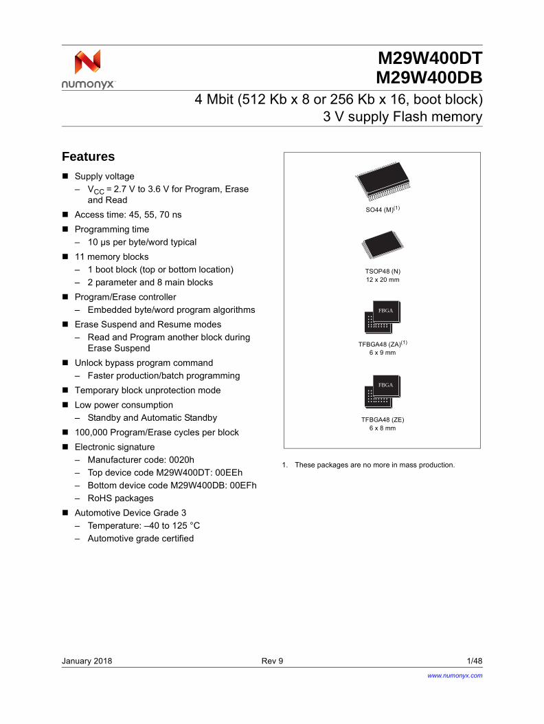
January 2018 Rev 9 1/48 1 M29W400DT M29W400DB 4 Mbit (512 Kb x 8 or 256 Kb x 16, boot block) 3 V supply Flash memory Features Supply voltage – V CC = 2.7 V to 3.6 V for Program, Erase and Read Access time: 45, 55, 70 ns Programming time – 10 μs per byte/word typical 11 memory blocks – 1 boot block (top or bottom location) – 2 parameter and 8 main blocks Program/Erase controller – Embedded byte/word program algorithms Erase Suspend and Resume modes – Read and Program another block during Erase Suspend Unlock bypass program command – Faster production/batch programming Temporary block unprotection mode Low power consumption – Standby and Automatic Standby 100,000 Program/Erase cycles per block Electronic signature – Manufacturer code: 0020h – Top device code M29W400DT: 00EEh – Bottom device code M29W400DB: 00EFh – RoHS packages Automotive Device Grade 3 – Temperature: –40 to 125 °C – Automotive grade certified 1. These packages are no more in mass production. TFBGA48 (ZA) (1) 6 x 9 mm FBGA SO44 (M) (1) TFBGA48 (ZE) 6 x 8 mm TSOP48 (N) 12 x 20 mm FBGA www.numonyx.com
Transcript of M29W400DT M29W400DB · 2018-11-23 · Table 21: Top boot block addresses M29W400DT and M29W400DT...
January 2018 Rev 9 1/48
1
M29W400DTM29W400DB
4 Mbit (512 Kb x 8 or 256 Kb x 16, boot block)3 V supply Flash memory
Features
Supply voltage
– VCC = 2.7 V to 3.6 V for Program, Eraseand Read
Access time: 45, 55, 70 ns
Programming time
– 10 μs per byte/word typical
11 memory blocks
– 1 boot block (top or bottom location)
– 2 parameter and 8 main blocks
Program/Erase controller
– Embedded byte/word program algorithms
Erase Suspend and Resume modes
– Read and Program another block duringErase Suspend
Unlock bypass program command
– Faster production/batch programming
Temporary block unprotection mode
Low power consumption
– Standby and Automatic Standby
100,000 Program/Erase cycles per block
Electronic signature
– Manufacturer code: 0020h
– Top device code M29W400DT: 00EEh
– Bottom device code M29W400DB: 00EFh
– RoHS packages
Automotive Device Grade 3
– Temperature: –40 to 125 °C
– Automotive grade certified
1. These packages are no more in mass production.
TFBGA48 (ZA)(1)
6 x 9 mm
FBGA
SO44 (M)(1)
TFBGA48 (ZE)6 x 8 mm
TSOP48 (N)12 x 20 mm
FBGA
www.numonyx.com
Contents M29W400DT, M29W400DB
2/48
Contents
1 Description . . . . . . . . . . . . . . . . . . . . . . . . . . . . . . . . . . . . . . . . . . . . . . . . . 6
2 Signal descriptions . . . . . . . . . . . . . . . . . . . . . . . . . . . . . . . . . . . . . . . . . 13
2.1 Address inputs (A0-A17) . . . . . . . . . . . . . . . . . . . . . . . . . . . . . . . . . . . . . 13
2.2 Data inputs/outputs (DQ0-DQ7) . . . . . . . . . . . . . . . . . . . . . . . . . . . . . . . . 13
2.3 Data inputs/outputs (DQ8-DQ14) . . . . . . . . . . . . . . . . . . . . . . . . . . . . . . . 13
2.4 Data input/output or Address input (DQ15A-1) . . . . . . . . . . . . . . . . . . . . 13
2.5 Chip Enable (E) . . . . . . . . . . . . . . . . . . . . . . . . . . . . . . . . . . . . . . . . . . . . 13
2.6 Output Enable (G) . . . . . . . . . . . . . . . . . . . . . . . . . . . . . . . . . . . . . . . . . . 13
2.7 Write Enable (W) . . . . . . . . . . . . . . . . . . . . . . . . . . . . . . . . . . . . . . . . . . . 14
2.8 Reset/Block Temporary Unprotect (RP) . . . . . . . . . . . . . . . . . . . . . . . . . . 14
2.9 Ready/Busy output (RB) . . . . . . . . . . . . . . . . . . . . . . . . . . . . . . . . . . . . . . 14
2.10 Byte/Word Organization Select (BYTE) . . . . . . . . . . . . . . . . . . . . . . . . . . 14
2.11 VCC supply voltage . . . . . . . . . . . . . . . . . . . . . . . . . . . . . . . . . . . . . . . . . . 15
2.12 VSS ground . . . . . . . . . . . . . . . . . . . . . . . . . . . . . . . . . . . . . . . . . . . . . . . . 15
3 Bus operations . . . . . . . . . . . . . . . . . . . . . . . . . . . . . . . . . . . . . . . . . . . . 16
3.1 Bus Read . . . . . . . . . . . . . . . . . . . . . . . . . . . . . . . . . . . . . . . . . . . . . . . . . 16
3.2 Bus Write . . . . . . . . . . . . . . . . . . . . . . . . . . . . . . . . . . . . . . . . . . . . . . . . . 16
3.3 Output Disable . . . . . . . . . . . . . . . . . . . . . . . . . . . . . . . . . . . . . . . . . . . . . 16
3.4 Standby . . . . . . . . . . . . . . . . . . . . . . . . . . . . . . . . . . . . . . . . . . . . . . . . . . 16
3.5 Automatic Standby . . . . . . . . . . . . . . . . . . . . . . . . . . . . . . . . . . . . . . . . . . 16
3.6 Special bus operations . . . . . . . . . . . . . . . . . . . . . . . . . . . . . . . . . . . . . . . 17
3.7 Electronic signature . . . . . . . . . . . . . . . . . . . . . . . . . . . . . . . . . . . . . . . . . 17
3.8 Block protection and blocks unprotection . . . . . . . . . . . . . . . . . . . . . . . . . 17
4 Command interface . . . . . . . . . . . . . . . . . . . . . . . . . . . . . . . . . . . . . . . . . 19
4.1 Read/Reset command . . . . . . . . . . . . . . . . . . . . . . . . . . . . . . . . . . . . . . . 19
4.2 Auto Select command . . . . . . . . . . . . . . . . . . . . . . . . . . . . . . . . . . . . . . . 19
4.3 Program command . . . . . . . . . . . . . . . . . . . . . . . . . . . . . . . . . . . . . . . . . . 19
4.4 Unlock Bypass command . . . . . . . . . . . . . . . . . . . . . . . . . . . . . . . . . . . . . 20
4.5 Unlock Bypass Program command . . . . . . . . . . . . . . . . . . . . . . . . . . . . . 20
M29W400DT, M29W400DB Contents
3/48
4.6 Unlock Bypass Reset command . . . . . . . . . . . . . . . . . . . . . . . . . . . . . . . 20
4.7 Chip Erase command . . . . . . . . . . . . . . . . . . . . . . . . . . . . . . . . . . . . . . . . 20
4.8 Block Erase command . . . . . . . . . . . . . . . . . . . . . . . . . . . . . . . . . . . . . . . 21
4.9 Erase Suspend command . . . . . . . . . . . . . . . . . . . . . . . . . . . . . . . . . . . . 21
4.10 Erase Resume command . . . . . . . . . . . . . . . . . . . . . . . . . . . . . . . . . . . . . 22
4.11 Block Protect and Chip Unprotect commands . . . . . . . . . . . . . . . . . . . . . 22
5 Status Register . . . . . . . . . . . . . . . . . . . . . . . . . . . . . . . . . . . . . . . . . . . . 24
5.1 Data Polling bit (DQ7) . . . . . . . . . . . . . . . . . . . . . . . . . . . . . . . . . . . . . . . 24
5.2 Toggle bit (DQ6) . . . . . . . . . . . . . . . . . . . . . . . . . . . . . . . . . . . . . . . . . . . . 24
5.3 Error bit (DQ5) . . . . . . . . . . . . . . . . . . . . . . . . . . . . . . . . . . . . . . . . . . . . . 25
5.4 Erase Timer bit (DQ3) . . . . . . . . . . . . . . . . . . . . . . . . . . . . . . . . . . . . . . . 25
5.5 Alternative Toggle bit (DQ2) . . . . . . . . . . . . . . . . . . . . . . . . . . . . . . . . . . . 25
6 Maximum rating . . . . . . . . . . . . . . . . . . . . . . . . . . . . . . . . . . . . . . . . . . . . 28
7 DC and AC parameters . . . . . . . . . . . . . . . . . . . . . . . . . . . . . . . . . . . . . . 29
8 Package mechanical . . . . . . . . . . . . . . . . . . . . . . . . . . . . . . . . . . . . . . . . 35
9 Part numbering . . . . . . . . . . . . . . . . . . . . . . . . . . . . . . . . . . . . . . . . . . . . 39
Appendix A Block address table . . . . . . . . . . . . . . . . . . . . . . . . . . . . . . . . . . . . . . 40
Appendix B Block protection. . . . . . . . . . . . . . . . . . . . . . . . . . . . . . . . . . . . . . . . . 41
B.1 Programmer technique . . . . . . . . . . . . . . . . . . . . . . . . . . . . . . . . . . . . . . . 41
B.2 In-system technique . . . . . . . . . . . . . . . . . . . . . . . . . . . . . . . . . . . . . . . . . 41
10 Revision history . . . . . . . . . . . . . . . . . . . . . . . . . . . . . . . . . . . . . . . . . . . 47
List of tables M29W400DT, M29W400DB
4/48
List of tables
Table 1. Signal names . . . . . . . . . . . . . . . . . . . . . . . . . . . . . . . . . . . . . . . . . . . . . . . . . . . . . . . . . . . . 7Table 2. Bus operations, BYTE = VIL . . . . . . . . . . . . . . . . . . . . . . . . . . . . . . . . . . . . . . . . . . . . . . . . 17Table 3. Bus operations, BYTE = VIH. . . . . . . . . . . . . . . . . . . . . . . . . . . . . . . . . . . . . . . . . . . . . . . . . . . . . . . . . . . . . 18Table 4. Program, Erase times and Program, Erase endurance cycles. . . . . . . . . . . . . . . . . . . . . . 22Table 5. Commands, 16-bit mode, BYTE = VIH . . . . . . . . . . . . . . . . . . . . . . . . . . . . . . . . . . . . . . . . 23Table 6. Commands, 8-bit mode, BYTE = VIL . . . . . . . . . . . . . . . . . . . . . . . . . . . . . . . . . . . . . . . . . 23Table 7. Status Register bits. . . . . . . . . . . . . . . . . . . . . . . . . . . . . . . . . . . . . . . . . . . . . . . . . . . . . . . 25Table 8. Absolute maximum ratings . . . . . . . . . . . . . . . . . . . . . . . . . . . . . . . . . . . . . . . . . . . . . . . . . 28Table 9. Operating and AC measurement conditions. . . . . . . . . . . . . . . . . . . . . . . . . . . . . . . . . . . . 29Table 10. Device capacitance. . . . . . . . . . . . . . . . . . . . . . . . . . . . . . . . . . . . . . . . . . . . . . . . . . . . . . . 30Table 11. DC characteristics. . . . . . . . . . . . . . . . . . . . . . . . . . . . . . . . . . . . . . . . . . . . . . . . . . . . . . . . 30Table 12. Read AC characteristics . . . . . . . . . . . . . . . . . . . . . . . . . . . . . . . . . . . . . . . . . . . . . . . . . . . 31Table 13. Write AC characteristics, Write Enable controlled . . . . . . . . . . . . . . . . . . . . . . . . . . . . . . . 32Table 14. Write AC characteristics, Chip Enable controlled . . . . . . . . . . . . . . . . . . . . . . . . . . . . . . . . 33Table 15. Reset/Block Temporary Unprotect AC characteristics . . . . . . . . . . . . . . . . . . . . . . . . . . . . 34Table 16. SO44 – 44 lead plastic small outline, 525 mils body width, package mechanical data . . . 35Table 17. TSOP48 – 48 lead plastic thin small outline, 12 x 20 mm, package mechanical data . . . . 36Table 18. TFBGA48 6 x 9 mm, 6 x 8 active ball array, 0.80 mm pitch, package mechanical data. . . 37Table 19. TFBGA48 6 x 8 mm, 6 x 8 active ball array, 0.80 mm pitch, package mechanical data. . . 38Table 20. Ordering information scheme . . . . . . . . . . . . . . . . . . . . . . . . . . . . . . . . . . . . . . . . . . . . . . . 39Table 21. Top boot block addresses M29W400DT . . . . . . . . . . . . . . . . . . . . . . . . . . . . . . . . . . . . . . 40Table 22. Bottom boot block addresses M29W400DB . . . . . . . . . . . . . . . . . . . . . . . . . . . . . . . . . . . . 40Table 23. Programmer technique bus operations, BYTE = VIH or VIL . . . . . . . . . . . . . . . . . . . . . . . . . . . . . . . 42Table 24. Document revision history . . . . . . . . . . . . . . . . . . . . . . . . . . . . . . . . . . . . . . . . . . . . . . . . . 47
M29W400DT, M29W400DB List of figures
5/48
List of figures
Figure 1. Logic diagram . . . . . . . . . . . . . . . . . . . . . . . . . . . . . . . . . . . . . . . . . . . . . . . . . . . . . . . . . . . . 7Figure 2. SO connections . . . . . . . . . . . . . . . . . . . . . . . . . . . . . . . . . . . . . . . . . . . . . . . . . . . . . . . . . . 8Figure 3. TSOP connections . . . . . . . . . . . . . . . . . . . . . . . . . . . . . . . . . . . . . . . . . . . . . . . . . . . . . . . . 9Figure 4. TFBGA connections (top view through package) . . . . . . . . . . . . . . . . . . . . . . . . . . . . . . . . 10Figure 5. Block addresses (x 8) . . . . . . . . . . . . . . . . . . . . . . . . . . . . . . . . . . . . . . . . . . . . . . . . . . . . . 11Figure 6. Block addresses (x 16) . . . . . . . . . . . . . . . . . . . . . . . . . . . . . . . . . . . . . . . . . . . . . . . . . . . . 12Figure 7. Data polling flowchart . . . . . . . . . . . . . . . . . . . . . . . . . . . . . . . . . . . . . . . . . . . . . . . . . . . . . 26Figure 8. Data toggle flowchart . . . . . . . . . . . . . . . . . . . . . . . . . . . . . . . . . . . . . . . . . . . . . . . . . . . . . 27Figure 9. AC measurement I/O waveform . . . . . . . . . . . . . . . . . . . . . . . . . . . . . . . . . . . . . . . . . . . . . 29Figure 10. AC measurement load circuit . . . . . . . . . . . . . . . . . . . . . . . . . . . . . . . . . . . . . . . . . . . . . . . 29Figure 11. Read mode AC waveforms . . . . . . . . . . . . . . . . . . . . . . . . . . . . . . . . . . . . . . . . . . . . . . . . . 30Figure 12. Write AC waveforms, Write Enable controlled . . . . . . . . . . . . . . . . . . . . . . . . . . . . . . . . . . 32Figure 13. Write AC waveforms, Chip Enable controlled . . . . . . . . . . . . . . . . . . . . . . . . . . . . . . . . . . . 33Figure 14. Reset/Block Temporary Unprotect AC waveforms . . . . . . . . . . . . . . . . . . . . . . . . . . . . . . . 34Figure 15. SO44 - 44 lead plastic small outline, 525 mils body width, package outline. . . . . . . . . . . . 35Figure 16. TSOP48 – 48 lead plastic thin small outline, 12 x 20 mm, package outline . . . . . . . . . . . . 36Figure 17. TFBGA48 6 x 9 mm, 6 x 8 active ball array, 0.80 mm pitch, bottom view package outline 37Figure 18. TFBGA48 6 x 8 mm, 6 x 8 active ball array, 0.80 mm pitch, bottom view package outline 38Figure 19. Programmer equipment block protect flowchart . . . . . . . . . . . . . . . . . . . . . . . . . . . . . . . . . 43Figure 20. Programmer equipment chip unprotect flowchart . . . . . . . . . . . . . . . . . . . . . . . . . . . . . . . . 44Figure 21. In-system equipment block protect flowchart . . . . . . . . . . . . . . . . . . . . . . . . . . . . . . . . . . . 45Figure 22. In-system equipment chip unprotect flowchart . . . . . . . . . . . . . . . . . . . . . . . . . . . . . . . . . . 46
Important Notes and Warnings
Important Notes and Warnings
Micron Technology, Inc. ("Micron") reserves the right to make changes to information published in this
document, including without limitation specifications and product descriptions. This document
supersedes and replaces all information supplied prior to the publication hereof. You may not rely on any
information set forth in this document if you obtain the product described herein from any unauthorized
distributor or other source not authorized by Micron.
Automotive Applications. Products are not designed or intended for use in automotive applications
unless specifically designated by Micron as automotive-grade by their respective data sheets. Distributor
and customer/distributor shall assume the sole risk and liability for and shall indemnify and hold Micron
harmless against all claims, costs, damages, and expenses and reasonable attorneys' fees arising out of,
directly or indirectly, any claim of product liability, personal injury, death, or property damage resulting
directly or indirectly from any use of nonautomotive-grade products in automotive applications.
Customer/distributor shall ensure that the terms and conditions of sale between customer/distributor and
any customer of distributor/customer (1) state that Micron products are not designed or intended for use
in automotive applications unless specifically designated by Micron as automotive-grade by their
respective data sheets and (2) require such customer of distributor/customer to indemnify and hold
Micron harmless against all claims, costs, damages, and expenses and reasonable attorneys' fees
arising out of, directly or indirectly, any claim of product liability, personal injury, death, or property
damage resulting from any use of non-automotive-grade products in automotive applications.
Critical Applications. Products are not authorized for use in applications in which failure of the Micron
component could result, directly or indirectly in death, personal injury, or severe property or
environmental damage ("Critical Applications"). Customer must protect against death, personal injury,
and severe property and environmental damage by incorporating safety design measures into
customer's applications to ensure that failure of the Micron component will not result in such harms.
Should customer or distributor purchase, use, or sell any Micron component for any critical application,
customer and distributor shall indemnify and hold harmless Micron and its subsidiaries, subcontractors,
and affiliates and the directors, officers, and employees of each against all claims, costs, damages, and
expenses and reasonable attorneys' fees arising out of, directly or indirectly, any claim of product liability,
personal injury, or death arising in any way out of such critical application, whether or not Micron or its
subsidiaries, subcontractors, or affiliates were negligent in the design, manufacture, or warning of the
Micron product.
Customer Responsibility. Customers are responsible for the design, manufacture, and operation of
their systems, applications, and products using Micron products. ALL SEMICONDUCTOR PRODUCTS
HAVE INHERENT FAILURE RATES AND LIMITED USEFUL LIVES. IT IS THE CUSTOMER'S SOLE
RESPONSIBILITY TO DETERMINE WHETHER THE MICRON PRODUCT IS SUITABLE AND FIT FOR
THE CUSTOMER'S SYSTEM, APPLICATION, OR PRODUCT. Customers must ensure that adequate
design, manufacturing, and operating safeguards are included in customer's applications and products to
eliminate the risk that personal injury, death, or severe property or environmental damages will result
from failure of any semiconductor component.
Limited Warranty. In no event shall Micron be liable for any indirect, incidental, punitive, special or
consequential damages (including without limitation lost profits, lost savings, business interruption, costs
related to the removal or replacement of any products or rework charges) whether or not such damages
are based on tort, warranty, breach of contract or other legal theory, unless explicitly stated in a written
agreement executed by Micron's duly authorized representative.
Description M29W400DT, M29W400DB
6/48
1 Description
The M29W400D is a 4 Mbit (512 K x 8 or 256 K x 16) non-volatile memory that can be read, erased and reprogrammed. These operations can be performed using a single low voltage (2.7 to 3.6 V) supply. On power-up the memory defaults to its Read mode where it can be read in the same way as a ROM or EPROM.
The memory is divided into blocks that can be erased independently so it is possible to preserve valid data while old data is erased. Each block can be protected independently to prevent accidental Program or Erase commands from modifying the memory. Program and Erase commands are written to the command interface of the memory. An on-chip Program/Erase controller simplifies the process of programming or erasing the memory by taking care of all of the special operations that are required to update the memory contents.
The end of a program or erase operation can be detected and any error conditions identified. The command set required to control the memory is consistent with JEDEC standards.
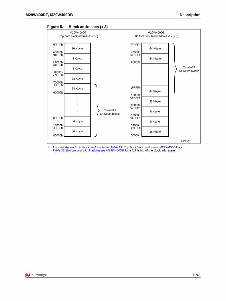
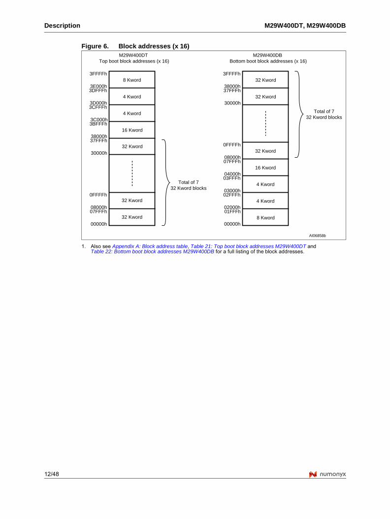
The blocks in the memory are asymmetrically arranged, see Figure 5 and Figure 6, Block addresses. The first or last 64 Kbytes have been divided into four additional blocks. The 16 Kbyte boot block can be used for small initialization code to start the microprocessor, the two 8 Kbyte parameter blocks can be used for parameter storage and the remaining 32 Kbyte is a small main block where the application may be stored.
Chip Enable, Output Enable and Write Enable signals control the bus operation of the memory. They allow simple connection to most microprocessors, often without additional logic.
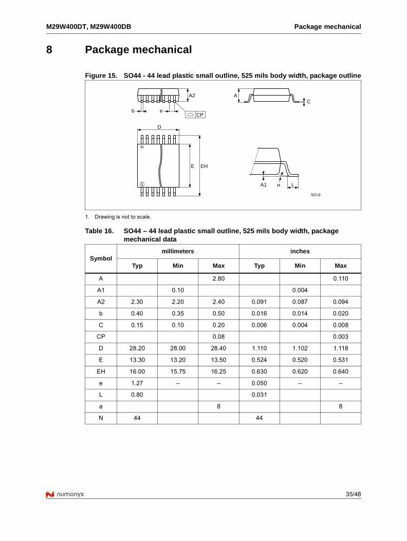
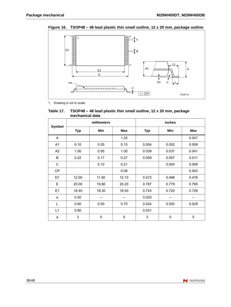
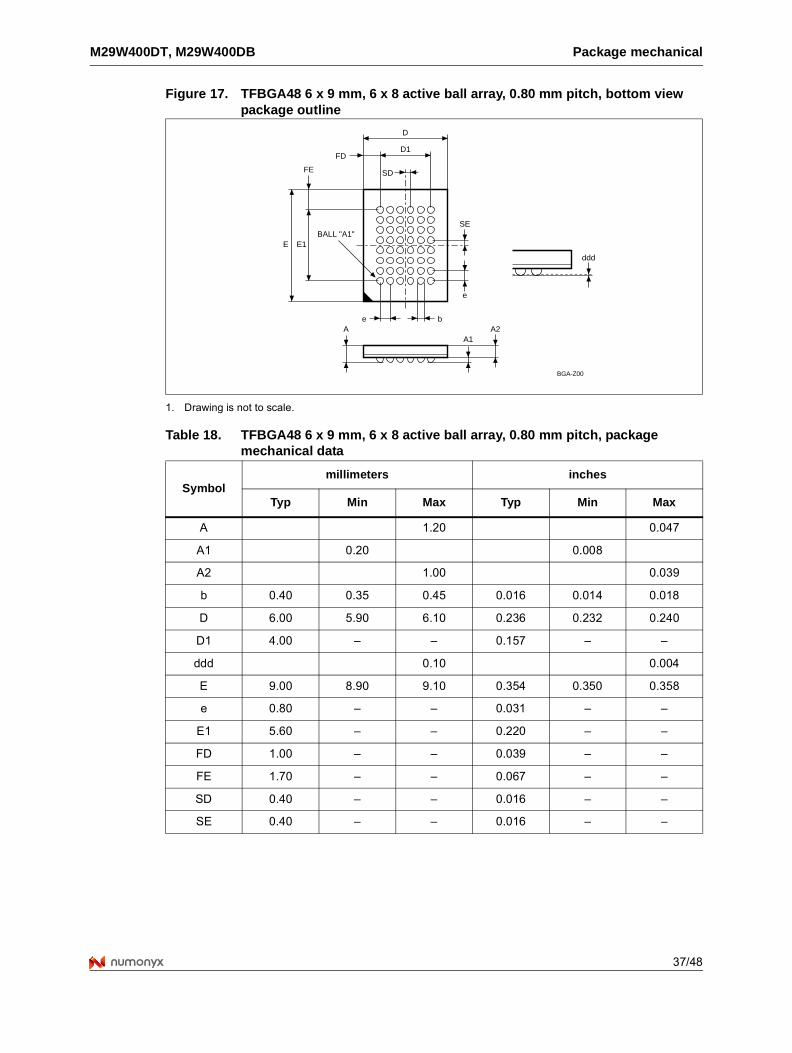
The memory is offered in SO44, TSOP48 (12 x 20 mm), TFBGA48 0.8 mm pitch (6 x 9 mm and 6 x 8 mm) packages. The memory is supplied with all the bits erased (set to ’1’).
In order to meet environmental requirements, Numonyx offers the M29W400D in RoHS packages, which are Lead-free. The category of second level interconnect is marked on the package and on the inner box label, in compliance with JEDEC Standard JESD97. The maximum ratings related to soldering conditions are also marked on the inner box label.
M29W400DT, M29W400DB Description
7/48
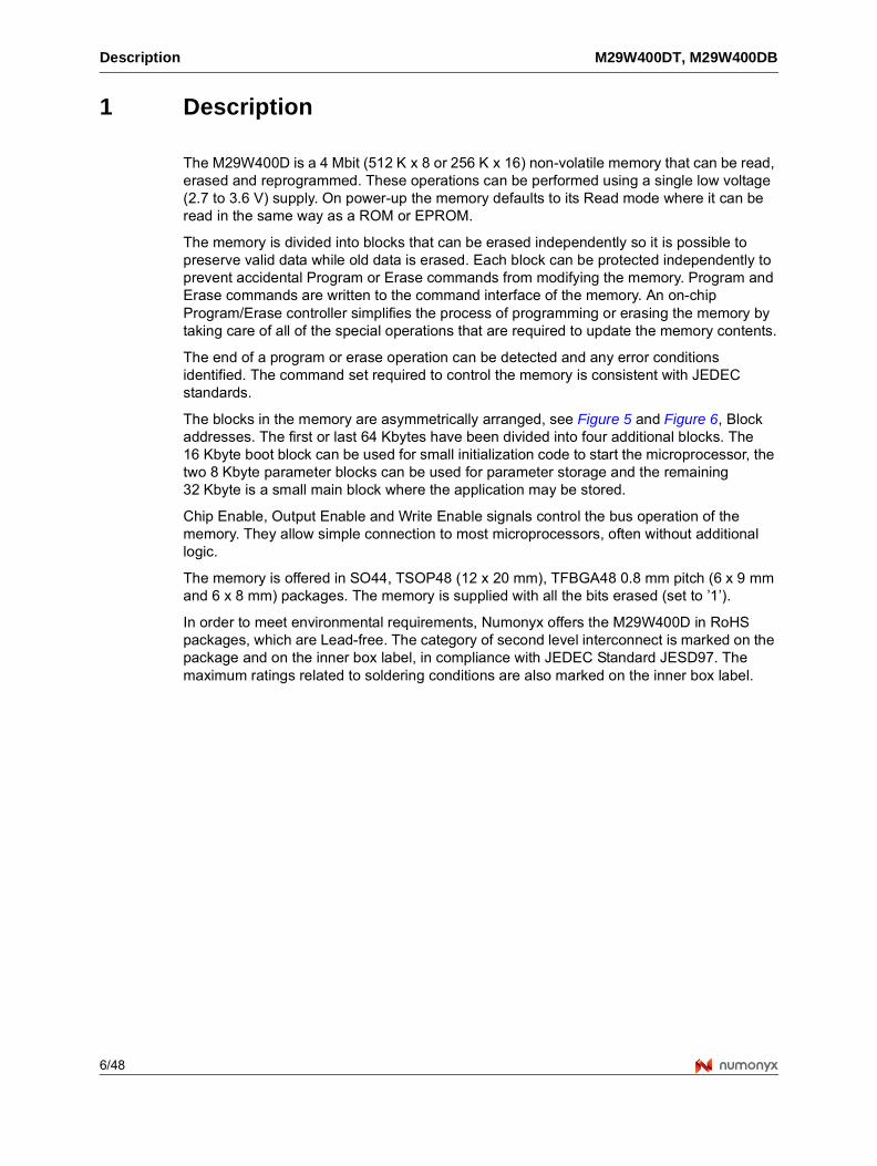
Figure 1. Logic diagram
Table 1. Signal names
Signal name Function Direction
A0-A17 Address inputs Inputs
DQ0-DQ7 Data inputs/outputs I/O
DQ8-DQ14 Data inputs/outputs I/O
DQ15A–1 Data input/output or Address input I/O
E Chip Enable Input
G Output Enable Input
W Write Enable Input
RP Reset/Block Temporary Unprotect Input
RB Ready/Busy output Output
BYTE Byte/word organization select Input
VCC Supply voltage
VSS Ground
NC Not connected internally
AI06853
18
A0-A17
W
DQ0-DQ14
VCC
M29W400DTM29W400DBE
VSS
15
G
RP
DQ15A–1
BYTE
RB
Description M29W400DT, M29W400DB
8/48
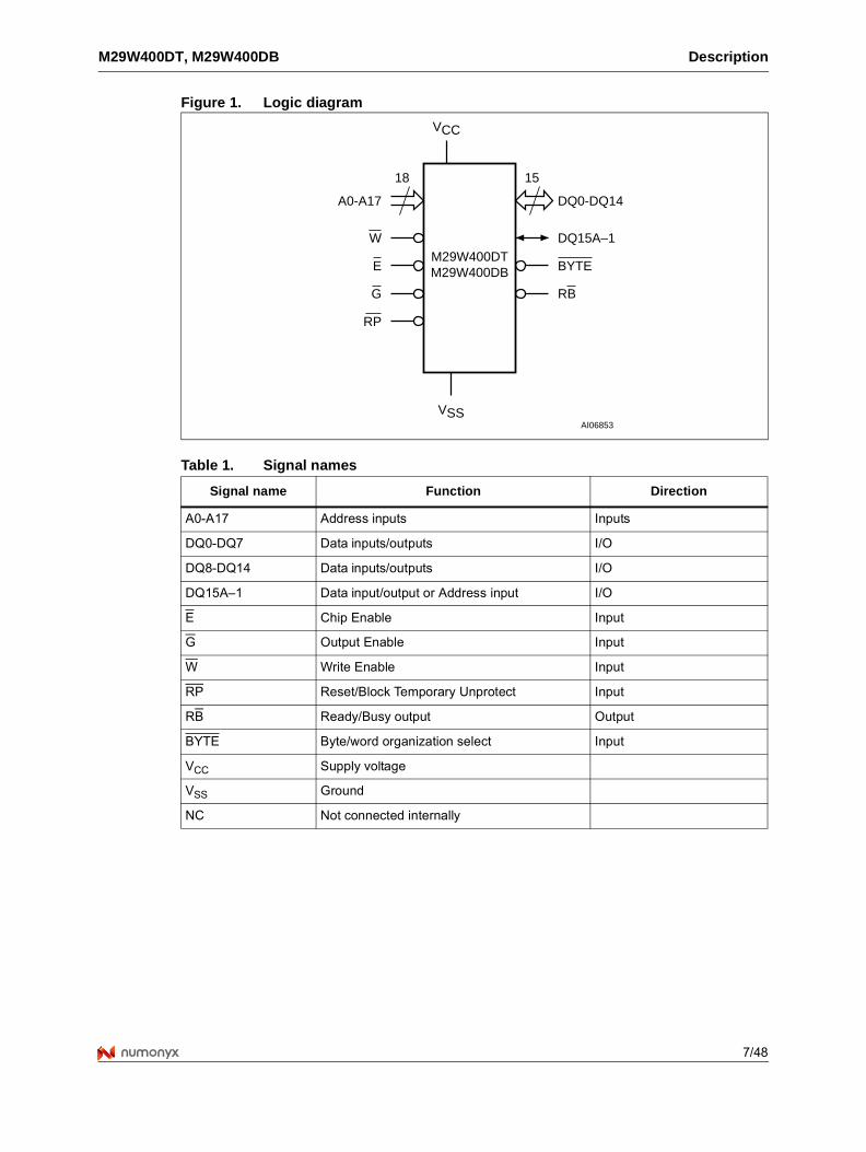
Figure 2. SO connections
1. NC = Not connected.
GDQ0DQ8
A3
A0E
VSS
A2A1
A13
VSS
A14A15
DQ7
A12
A16BYTE
DQ15A–1
DQ5DQ2
DQ3VCCDQ11DQ4
DQ14
A9
WRB
A4
RP
A7
AI06855
M29W400DTM29W400DB
8
234567
910111213141516
3231302928272625242322
20191817DQ1
DQ9
A6A5
DQ6DQ13
44
39383736353433
A11A10
DQ1021
DQ12
40
431
4241
A17 A8
NC
M29W400DT, M29W400DB Description
9/48
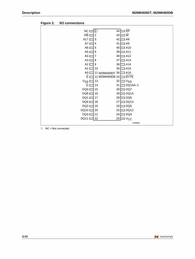
Figure 3. TSOP connections
1. NC = Not connected.
DQ3
DQ9DQ2
A6DQ0
W
A3
RB
DQ6A8A9
DQ13
A17
A10 DQ14
A2
DQ12
DQ10
DQ15A–1
VCC
DQ4
DQ5
A7
DQ7
NCNC
AI06854
M29W400DTM29W400DB
12
1
13
24 25
3637
48
DQ8
NCNC
A1
NC
A4A5
DQ1
DQ11
G
A12A13
A16
A11
BYTEA15A14
VSS
EA0
RP
VSS
Description M29W400DT, M29W400DB
10/48
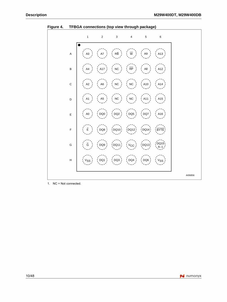
Figure 4. TFBGA connections (top view through package)
1. NC = Not connected.
AI06856
B
A
4321
G
F
H
DQ15A–1
A7A3
DQ10DQ8E
DQ13DQ11DQ9G
VSSDQ6DQ1VSS
DQ14
A12NCA17A4
A14A10NCNCA6A2
RP A8
DQ4DQ3
VCC
DQ12
A9
BYTE
A15A11NCA1
A16DQ7DQ5DQ2A0
NC
DQ0
A5
E
D
C
RB W A13
65
M29W400DT, M29W400DB Description
11/48
Figure 5. Block addresses (x 8)
1. Also see Appendix A: Block address table, Table 21: Top boot block addresses M29W400DT and Table 22: Bottom boot block addresses M29W400DB for a full listing of the block addresses.
AI06857b
16 Kbyte7FFFFh
7C000h
64 Kbyte
1FFFFh
10000h
64 Kbyte0FFFFh
00000h
M29W400DT Top boot block addresses (x 8)
32 Kbyte77FFFh
70000h
64 Kbyte60000h
6FFFFh
Total of 764 Kbyte blocks
16 Kbyte
7FFFFh
70000h64 Kbyte
64 Kbyte
03FFFh
00000h
M29W400DB Bottom boot block addresses (x 8)
32 Kbyte
6FFFFh
1FFFFh64 Kbyte
60000h
10000h
Total of 764 Kbyte blocks
0FFFFh
08000h
8 Kbyte
8 Kbyte
7BFFFh
7A000h79FFFh
78000h
8 Kbyte
8 Kbyte
07FFFh
06000h05FFFh
04000h
Description M29W400DT, M29W400DB
12/48
Figure 6. Block addresses (x 16)
1. Also see Appendix A: Block address table, Table 21: Top boot block addresses M29W400DT and Table 22: Bottom boot block addresses M29W400DB for a full listing of the block addresses.
AI06858b
8 Kword3FFFFh
3E000h
32 Kword
0FFFFh
08000h
32 Kword07FFFh
00000h
M29W400DT Top boot block addresses (x 16)
16 Kword3BFFFh
38000h
32 Kword30000h
37FFFh
Total of 732 Kword blocks
8 Kword
3FFFFh
38000h32 Kword
32 Kword
01FFFh
00000h
M29W400DB Bottom boot block addresses (x 16)
16 Kword
37FFFh
0FFFFh32 Kword
30000h
08000h
Total of 732 Kword blocks
07FFFh
04000h
4 Kword
4 Kword
3DFFFh
3D000h3CFFFh
3C000h
4 Kword
4 Kword
03FFFh
03000h02FFFh
02000h
M29W400DT, M29W400DB Signal descriptions
13/48
2 Signal descriptions
See Figure 1: Logic diagram, and Table : , for a brief overview of the signals connected to this device.
2.1 Address inputs (A0-A17)
The Address inputs select the cells in the memory array to access during Bus Read operations. During Bus Write operations they control the commands sent to the command interface of the Program/Erase controller.
2.2 Data inputs/outputs (DQ0-DQ7)
The Data inputs/outputs output the data stored at the selected address during a Bus Read operation. During Bus Write operations they represent the commands sent to the command interface of the Program/Erase controller.
2.3 Data inputs/outputs (DQ8-DQ14)
The Data inputs/outputs output the data stored at the selected address during a Bus Read operation when BYTE is High, VIH. When BYTE is Low, VIL, these pins are not used and are high impedance. During Bus Write operations the Command Register does not use these bits. When reading the Status Register these bits should be ignored.
2.4 Data input/output or Address input (DQ15A-1)
When BYTE is High, VIH, this pin behaves as a Data input/output pin (as DQ8-DQ14). When BYTE is Low, VIL, this pin behaves as an address pin; DQ15A–1 Low will select the LSB of the word on the other addresses, DQ15A–1 High will select the MSB. Throughout the text consider references to the Data input/output to include this pin when BYTE is High and references to the Address inputs to include this pin when BYTE is Low except when stated explicitly otherwise.
2.5 Chip Enable (E)
The Chip Enable, E, activates the memory, allowing Bus Read and Bus Write operations to be performed. When Chip Enable is High, VIH, all other pins are ignored.
2.6 Output Enable (G)
The Output Enable, G, controls the Bus Read operation of the memory.
Signal descriptions M29W400DT, M29W400DB
14/48
2.7 Write Enable (W)
The Write Enable, W, controls the Bus Write operation of the memory’s command interface.
2.8 Reset/Block Temporary Unprotect (RP)
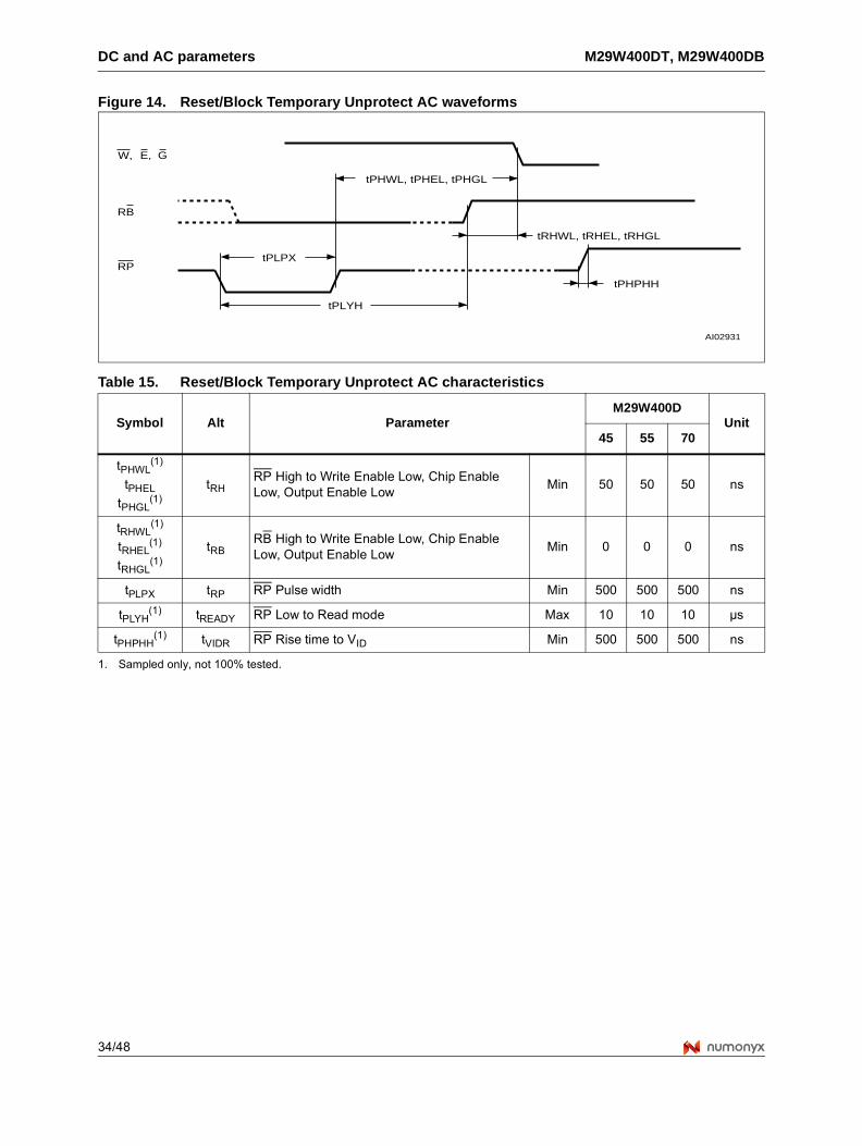
The Reset/Block Temporary Unprotect pin can be used to apply a hardware reset to the memory or to temporarily unprotect all blocks that have been protected.
A hardware reset is achieved by holding Reset/Block Temporary Unprotect Low, VIL, for at least tPLPX. After Reset/Block Temporary Unprotect goes High, VIH, the memory will be ready for Bus Read and Bus Write operations after tPHEL or tRHEL, whichever occurs last. See the Ready/Busy output section, Table 15: Reset/Block Temporary Unprotect AC characteristics and Figure 14: Reset/Block Temporary Unprotect AC waveforms, for more details.
Holding RP at VID will temporarily unprotect the protected blocks in the memory. Program and Erase operations on all blocks will be possible. The transition from VIH to VID must be slower than tPHPHH.
2.9 Ready/Busy output (RB)
The Ready/Busy pin is an open-drain output that can be used to identify when the memory array can be read. Ready/Busy is high-impedance during Read mode, Auto Select mode and Erase Suspend mode.
After a Hardware Reset, Bus Read and Bus Write operations cannot begin until Ready/Busy becomes high-impedance. See Table 15: Reset/Block Temporary Unprotect AC characteristics and Figure 14: Reset/Block Temporary Unprotect AC waveforms.
During Program or Erase operations Ready/Busy is Low, VOL. Ready/Busy will remain Low during Read/Reset commands or hardware resets until the memory is ready to enter Read mode.
2.10 Byte/Word Organization Select (BYTE)
The Byte/Word Organization Select pin is used to switch between the 8-bit and 16-bit Bus modes of the memory. When Byte/Word Organization Select is Low, VIL, the memory is in 8-bit mode, when it is High, VIH, the memory is in 16-bit mode.
M29W400DT, M29W400DB Signal descriptions
15/48
2.11 VCC supply voltage
The VCC supply voltage supplies the power for all operations (Read, Program, Erase etc.).
The command interface is disabled when the VCC supply voltage is less than the lockout voltage, VLKO. This prevents Bus Write operations from accidentally damaging the data during power-up, power-down and power surges. If the Program/Erase controller is programming or erasing during this time then the operation aborts and the memory contents being altered will be invalid.
A 0.1 μF capacitor should be connected between the VCC supply voltage pin and the VSS ground pin to decouple the current surges from the power supply. The PCB track widths must be sufficient to carry the currents required during program and erase operations, ICC3.
2.12 VSS ground
The VSS ground is the reference for all voltage measurements.
Bus operations M29W400DT, M29W400DB
16/48
3 Bus operations
There are five standard bus operations that control the device. These are Bus Read, Bus Write, Output Disable, Standby and Automatic Standby. See Table 2 and Table 3, Bus operations, for a summary. Typically glitches of less than 5 ns on Chip Enable or Write Enable are ignored by the memory and do not affect bus operations.
3.1 Bus Read
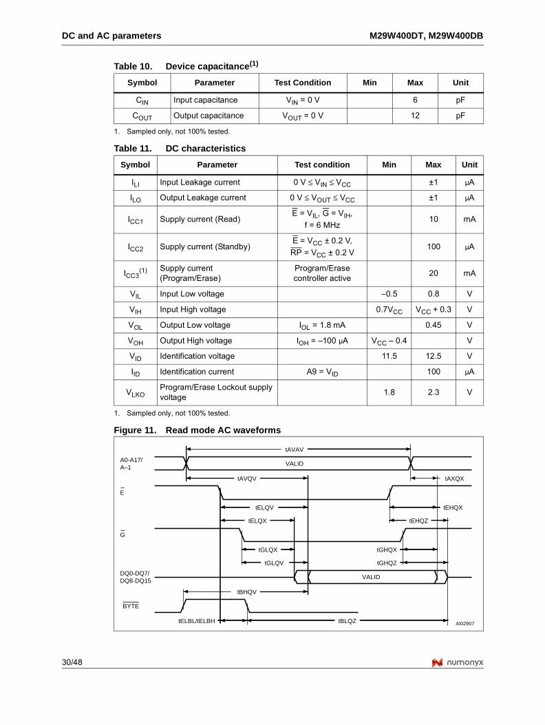
Bus Read operations read from the memory cells, or specific registers in the command interface. A valid Bus Read operation involves setting the desired address on the Address inputs, applying a Low signal, VIL, to Chip Enable and Output Enable and keeping Write Enable High, VIH. The Data inputs/outputs will output the value, see Figure 11: Read mode AC waveforms, and Table 12: Read AC characteristics, for details of when the output becomes valid.
3.2 Bus Write
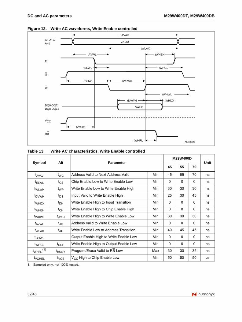
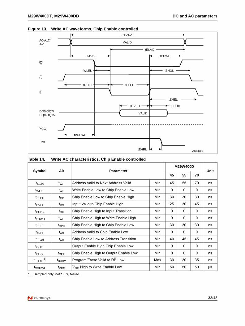
Bus Write operations write to the command interface. A valid Bus Write operation begins by setting the desired address on the Address inputs. The Address inputs are latched by the command interface on the falling edge of Chip Enable or Write Enable, whichever occurs last. The Data inputs/outputs are latched by the command interface on the rising edge of Chip Enable or Write Enable, whichever occurs first. Output Enable must remain High, VIH, during the whole Bus Write operation. See Figure 12 and Figure 13, Write AC waveforms, and Table 13 and Table 14, Write AC characteristics, for details of the timing requirements.
3.3 Output Disable
The Data inputs/outputs are in the high impedance state when Output Enable is High, VIH.
3.4 Standby
When Chip Enable is High, VIH, the memory enters Standby mode and the Data inputs/outputs pins are placed in the high-impedance state. To reduce the Supply current to the Standby Supply current, ICC2, Chip Enable should be held within VCC ± 0.2 V. For the Standby current level see Table 11: DC characteristics.
During program or erase operations the memory will continue to use the Program/Erase Supply current, ICC3, for Program or Erase operations until the operation completes.
3.5 Automatic Standby
If CMOS levels (VCC ± 0.2 V) are used to drive the bus and the bus is inactive for 150 ns or more the memory enters Automatic Standby where the internal Supply current is reduced to the Standby Supply current, ICC2. The Data inputs/outputs will still output data if a Bus Read operation is in progress.
M29W400DT, M29W400DB Bus operations
17/48
3.6 Special bus operations
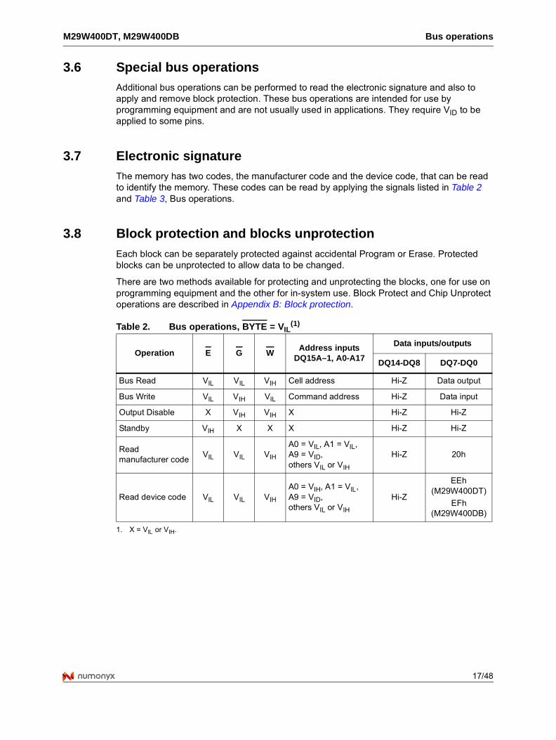
Additional bus operations can be performed to read the electronic signature and also to apply and remove block protection. These bus operations are intended for use by programming equipment and are not usually used in applications. They require VID to be applied to some pins.
3.7 Electronic signature
The memory has two codes, the manufacturer code and the device code, that can be read to identify the memory. These codes can be read by applying the signals listed in Table 2 and Table 3, Bus operations.
3.8 Block protection and blocks unprotection
Each block can be separately protected against accidental Program or Erase. Protected blocks can be unprotected to allow data to be changed.
There are two methods available for protecting and unprotecting the blocks, one for use on programming equipment and the other for in-system use. Block Protect and Chip Unprotect operations are described in Appendix B: Block protection.
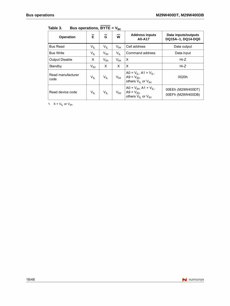
Table 2. Bus operations, BYTE = VIL(1)
1. X = VIL or VIH.
Operation E G WAddress inputs
DQ15A–1, A0-A17
Data inputs/outputs
DQ14-DQ8 DQ7-DQ0
Bus Read VIL VIL VIH Cell address Hi-Z Data output
Bus Write VIL VIH VIL Command address Hi-Z Data input
Output Disable X VIH VIH X Hi-Z Hi-Z
Standby VIH X X X Hi-Z Hi-Z
Read manufacturer code
VIL VIL VIH
A0 = VIL, A1 = VIL, A9 = VID,others VIL or VIH
Hi-Z 20h
Read device code VIL VIL VIH
A0 = VIH, A1 = VIL, A9 = VID, others VIL or VIH
Hi-Z
EEh (M29W400DT)
EFh (M29W400DB)
Bus operations M29W400DT, M29W400DB
18/48
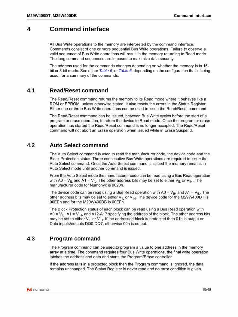
1. X = VIL or VIH.
Table 3. Bus operations, BYTE = VIH
Operation E G WAddress inputs
A0-A17Data inputs/outputs
DQ15A–1, DQ14-DQ0
Bus Read VIL VIL VIH Cell address Data output
Bus Write VIL VIH VIL Command address Data input
Output Disable X VIH VIH X Hi-Z
Standby VIH X X X Hi-Z
Read manufacturer code
VIL VIL VIH
A0 = VIL, A1 = VIL, A9 = VID, others VIL or VIH
0020h
Read device code VIL VIL VIH
A0 = VIH, A1 = VIL, A9 = VID,others VIL or VIH
00EEh (M29W400DT)
00EFh (M29W400DB)
M29W400DT, M29W400DB Command interface
19/48
4 Command interface
All Bus Write operations to the memory are interpreted by the command interface. Commands consist of one or more sequential Bus Write operations. Failure to observe a valid sequence of Bus Write operations will result in the memory returning to Read mode. The long command sequences are imposed to maximize data security.
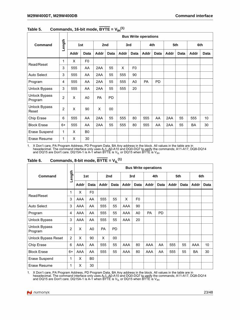
The address used for the commands changes depending on whether the memory is in 16-bit or 8-bit mode. See either Table 5, or Table 6, depending on the configuration that is being used, for a summary of the commands.
4.1 Read/Reset command
The Read/Reset command returns the memory to its Read mode where it behaves like a ROM or EPROM, unless otherwise stated. It also resets the errors in the Status Register. Either one or three Bus Write operations can be used to issue the Read/Reset command.
The Read/Reset command can be issued, between Bus Write cycles before the start of a program or erase operation, to return the device to Read mode. Once the program or erase operation has started the Read/Reset command is no longer accepted. The Read/Reset command will not abort an Erase operation when issued while in Erase Suspend.
4.2 Auto Select command
The Auto Select command is used to read the manufacturer code, the device code and the Block Protection status. Three consecutive Bus Write operations are required to issue the Auto Select command. Once the Auto Select command is issued the memory remains in Auto Select mode until another command is issued.
From the Auto Select mode the manufacturer code can be read using a Bus Read operation with A0 = VIL and A1 = VIL. The other address bits may be set to either VIL or VIH. The manufacturer code for Numonyx is 0020h.
The device code can be read using a Bus Read operation with A0 = VIH and A1 = VIL. The other address bits may be set to either VIL or VIH. The device code for the M29W400DT is 00EEh and for the M29W400DB is 00EFh.
The Block Protection status of each block can be read using a Bus Read operation with A0 = VIL, A1 = VIH, and A12-A17 specifying the address of the block. The other address bits may be set to either VIL or VIH. If the addressed block is protected then 01h is output on Data inputs/outputs DQ0-DQ7, otherwise 00h is output.
4.3 Program command
The Program command can be used to program a value to one address in the memory array at a time. The command requires four Bus Write operations, the final write operation latches the address and data and starts the Program/Erase controller.
If the address falls in a protected block then the Program command is ignored, the data remains unchanged. The Status Register is never read and no error condition is given.
Command interface M29W400DT, M29W400DB
20/48
During the program operation the memory will ignore all commands. It is not possible to issue any command to abort or pause the operation. Typical program times are given in Table 4: Program, Erase times and Program, Erase endurance cycles. Bus Read operations during the program operation will output the Status Register on the Data inputs/outputs. See the section on the Status Register for more details.
After the program operation has completed the memory will return to the Read mode, unless an error has occurred. When an error occurs the memory will continue to output the Status Register. A Read/Reset command must be issued to reset the error condition and return to Read mode.
Note that the Program command cannot change a bit set at ’0’ back to ’1’. One of the Erase commands must be used to set all the bits in a block or in the whole memory from ’0’ to ’1’.
4.4 Unlock Bypass command
The Unlock Bypass command is used in conjunction with the Unlock Bypass Program command to program the memory. When the access time to the device is long (as with some EPROM programmers) considerable time saving can be made by using these commands. Three Bus Write operations are required to issue the Unlock Bypass command.
Once the Unlock Bypass command has been issued the memory will only accept the Unlock Bypass Program command and the Unlock Bypass Reset command. The memory can be read as if in Read mode.
4.5 Unlock Bypass Program command
The Unlock Bypass Program command can be used to program one address in memory at a time. The command requires two Bus Write operations, the final write operation latches the address and data and starts the Program/Erase controller.
The Program operation using the Unlock Bypass Program command behaves identically to the Program operation using the Program command. A protected block cannot be programmed; the operation cannot be aborted and the Status Register is read. Errors must be reset using the Read/Reset command, which leaves the device in Unlock Bypass mode. See the Program command for details on the behavior.
4.6 Unlock Bypass Reset command
The Unlock Bypass Reset command can be used to return to Read/Reset mode from Unlock Bypass mode. Two Bus Write operations are required to issue the Unlock Bypass Reset command. Read/Reset command does not exit from Unlock Bypass mode.
4.7 Chip Erase command
The Chip Erase command can be used to erase the entire chip. Six Bus Write operations are required to issue the Chip Erase command and start the Program/Erase controller.
If any blocks are protected then these are ignored and all the other blocks are erased. If all of the blocks are protected the Chip Erase operation appears to start but will terminate
M29W400DT, M29W400DB Command interface
21/48
within about 100 μs, leaving the data unchanged. No error condition is given when protected blocks are ignored.
During the erase operation the memory will ignore all commands. It is not possible to issue any command to abort the operation. Typical chip erase times are given in Table 4. All Bus Read operations during the Chip Erase operation will output the Status Register on the Data inputs/outputs. See the section on the Status Register for more details.
After the Chip Erase operation has completed the memory will return to the Read mode, unless an error has occurred. When an error occurs the memory will continue to output the Status Register. A Read/Reset command must be issued to reset the error condition and return to Read mode.
The Chip Erase command sets all of the bits in unprotected blocks of the memory to ’1’. All previous data is lost.
4.8 Block Erase command
The Block Erase command can be used to erase a list of one or more blocks. Six Bus Write operations are required to select the first block in the list. Each additional block in the list can be selected by repeating the sixth Bus Write operation using the address of the additional block. The Block Erase operation starts the Program/Erase controller about 50 μs after the last Bus Write operation. Once the Program/Erase controller starts it is not possible to select any more blocks. Each additional block must therefore be selected within 50 μs of the last block. The 50 μs timer restarts when an additional block is selected. The Status Register can be read after the sixth Bus Write operation. See the Status Register for details on how to identify if the Program/Erase controller has started the Block Erase operation.
If any selected blocks are protected then these are ignored and all the other selected blocks are erased. If all of the selected blocks are protected the Block Erase operation appears to start but will terminate within about 100 μs, leaving the data unchanged. No error condition is given when protected blocks are ignored.
During the Block Erase operation the memory will ignore all commands except the Erase Suspend command. Typical block erase times are given in Table 4. All Bus Read operations during the Block Erase operation will output the Status Register on the Data inputs/outputs. See the section on the Status Register for more details.
After the Block Erase operation has completed the memory will return to the Read mode, unless an error has occurred. When an error occurs the memory will continue to output the Status Register. A Read/Reset command must be issued to reset the error condition and return to Read mode.
The Block Erase command sets all of the bits in the unprotected selected blocks to ’1’. All previous data in the selected blocks is lost.
4.9 Erase Suspend command
The Erase Suspend command may be used to temporarily suspend a Block Erase operation and return the memory to Read mode. The command requires one Bus Write operation.
The Program/Erase controller will suspend within the Erase Suspend Latency time after the Erase Suspend command is issued (see Table 4 for numerical values). Once the
Command interface M29W400DT, M29W400DB
22/48
Program/Erase controller has stopped the memory will be set to Read mode and the Erase will be suspended. If the Erase Suspend command is issued during the period when the memory is waiting for an additional block (before the Program/Erase controller starts) then the Erase is suspended immediately and will start immediately when the Erase Resume command is issued. It is not possible to select any further blocks to erase after the Erase Resume.
During Erase Suspend it is possible to Read and Program cells in blocks that are not being erased; both Read and Program operations behave as normal on these blocks. If any attempt is made to program in a protected block or in the suspended block then the Program command is ignored and the data remains unchanged. The Status Register is not read and no error condition is given. Reading from blocks that are being erased will output the Status Register.
It is also possible to issue the Auto Select and Unlock Bypass commands during an Erase Suspend. The Read/Reset command must be issued to return the device to Read Array mode before the Resume command will be accepted.
4.10 Erase Resume command
The Erase Resume command must be used to restart the Program/Erase controller from Erase Suspend. An erase can be suspended and resumed more than once.
4.11 Block Protect and Chip Unprotect commands
Each block can be separately protected against accidental program or erase. The whole chip can be unprotected to allow the data inside the blocks to be changed.
Block Protect and Chip Unprotect operations are described in Appendix B: Block protection.
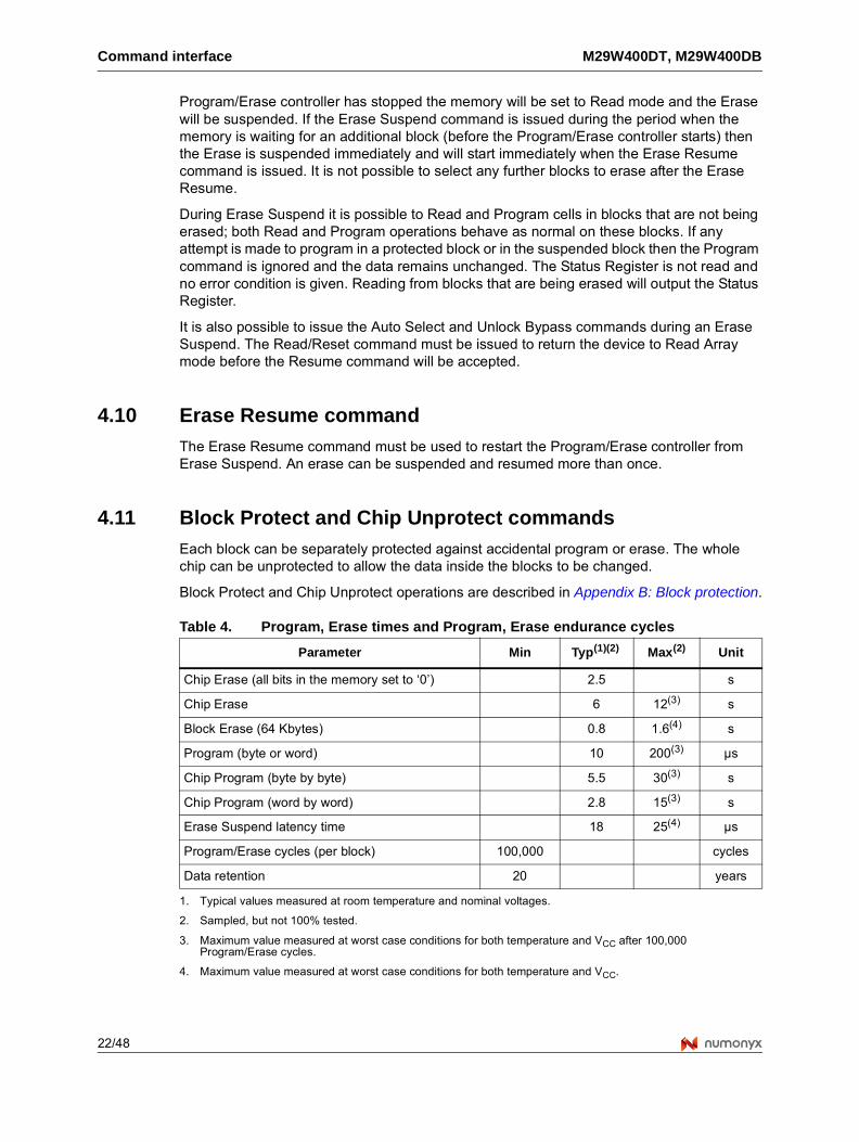
Table 4. Program, Erase times and Program, Erase endurance cycles
Parameter Min Typ(1)(2)
1. Typical values measured at room temperature and nominal voltages.
Max(2)
2. Sampled, but not 100% tested.
Unit
Chip Erase (all bits in the memory set to ‘0’) 2.5 s
Chip Erase 6 12(3)
3. Maximum value measured at worst case conditions for both temperature and VCC after 100,000 Program/Erase cycles.
s
Block Erase (64 Kbytes) 0.8 1.6(4)
4. Maximum value measured at worst case conditions for both temperature and VCC.
s
Program (byte or word) 10 200(3) μs
Chip Program (byte by byte) 5.5 30(3) s
Chip Program (word by word) 2.8 15(3) s
Erase Suspend latency time 18 25(4) μs
Program/Erase cycles (per block) 100,000 cycles
Data retention 20 years
M29W400DT, M29W400DB Command interface
23/48
Table 5. Commands, 16-bit mode, BYTE = VIH(1)
Command
Le
ng
th
Bus Write operations
1st 2nd 3rd 4th 5th 6th
Addr Data Addr Data Addr Data Addr Data Addr Data Addr Data
Read/Reset1 X F0
3 555 AA 2AA 55 X F0
Auto Select 3 555 AA 2AA 55 555 90
Program 4 555 AA 2AA 55 555 A0 PA PD
Unlock Bypass 3 555 AA 2AA 55 555 20
Unlock Bypass Program
2 X A0 PA PD
Unlock Bypass Reset
2 X 90 X 00
Chip Erase 6 555 AA 2AA 55 555 80 555 AA 2AA 55 555 10
Block Erase 6+ 555 AA 2AA 55 555 80 555 AA 2AA 55 BA 30
Erase Suspend 1 X B0
Erase Resume 1 X 30
1. X Don’t care, PA Program Address, PD Program Data, BA Any address in the block. All values in the table are in hexadecimal. The command interface only uses A-1; A0-A10 and DQ0-DQ7 to verify the commands; A11-A17, DQ8-DQ14 and DQ15 are Don't care. DQ15A-1 is A-1 when BYTE is VIL or DQ15 when BYTE is VIH.
Table 6. Commands, 8-bit mode, BYTE = VIL(1)
Command
Le
ng
th
Bus Write operations
1st 2nd 3rd 4th 5th 6th
Addr Data Addr Data Addr Data Addr Data Addr Data Addr Data
Read/Reset1 X F0
3 AAA AA 555 55 X F0
Auto Select 3 AAA AA 555 55 AAA 90
Program 4 AAA AA 555 55 AAA A0 PA PD
Unlock Bypass 3 AAA AA 555 55 AAA 20
Unlock Bypass Program
2 X A0 PA PD
Unlock Bypass Reset 2 X 90 X 00
Chip Erase 6 AAA AA 555 55 AAA 80 AAA AA 555 55 AAA 10
Block Erase 6+ AAA AA 555 55 AAA 80 AAA AA 555 55 BA 30
Erase Suspend 1 X B0
Erase Resume 1 X 30
1. X Don’t care, PA Program Address, PD Program Data, BA Any address in the block. All values in the table are in hexadecimal. The command interface only uses A-1; A0-A10 and DQ0-DQ7 to verify the commands; A11-A17, DQ8-DQ14 and DQ15 are Don't care. DQ15A-1 is A-1 when BYTE is VIL or DQ15 when BYTE is VIH.
Status Register M29W400DT, M29W400DB
24/48
5 Status Register
Bus Read operations from any address always read the Status Register during Program and Erase operations. It is also read during Erase Suspend when an address within a block being erased is accessed.
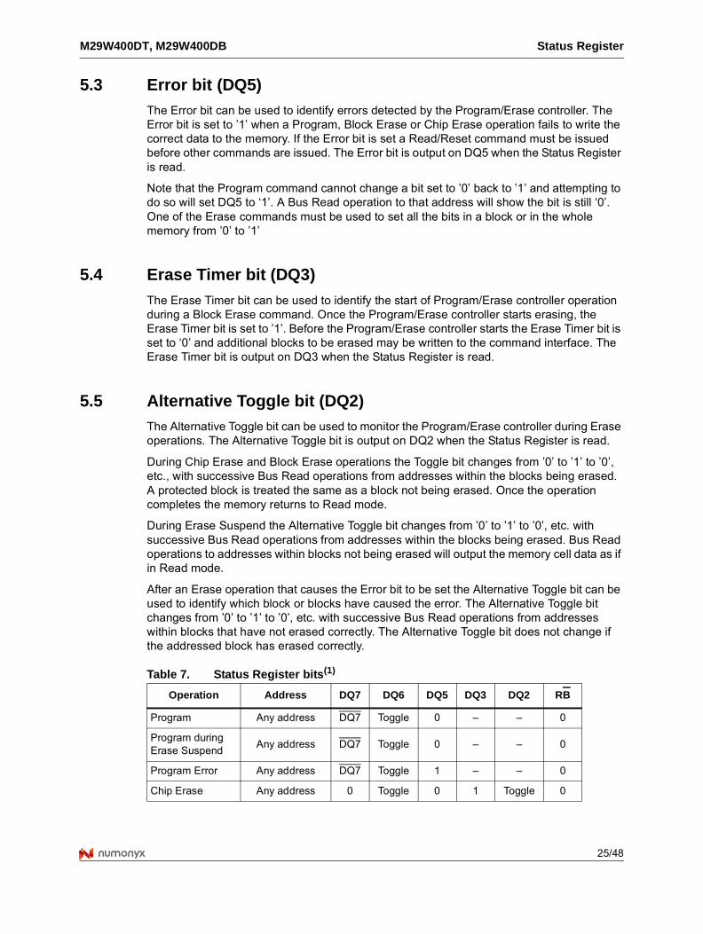
The bits in the Status Register are summarized in Table 7: Status Register bits.
5.1 Data Polling bit (DQ7)
The Data Polling bit can be used to identify whether the Program/Erase controller has successfully completed its operation or if it has responded to an Erase Suspend. The Data Polling bit is output on DQ7 when the Status Register is read.
During Program operations the Data Polling bit outputs the complement of the bit being programmed to DQ7. After successful completion of the Program operation the memory returns to Read mode and Bus Read operations from the address just programmed output DQ7, not its complement.
During Erase operations the Data Polling bit outputs ’0’, the complement of the erased state of DQ7. After successful completion of the Erase operation the memory returns to Read mode.
In Erase Suspend mode the Data Polling bit will output a ’1’ during a Bus Read operation within a block being erased. The Data Polling bit will change from a ’0’ to a ’1’ when the Program/Erase controller has suspended the Erase operation.
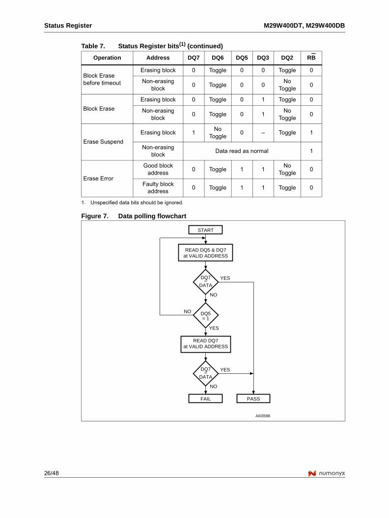
Figure 7: Data polling flowchart, gives an example of how to use the Data Polling bit. A valid address is the address being programmed or an address within the block being erased.
5.2 Toggle bit (DQ6)
The Toggle bit can be used to identify whether the Program/Erase controller has successfully completed its operation or if it has responded to an Erase Suspend. The Toggle bit is output on DQ6 when the Status Register is read.
During Program and Erase operations the Toggle bit changes from ’0’ to ’1’ to ’0’, etc., with successive Bus Read operations at any address. After successful completion of the operation the memory returns to Read mode.
During Erase Suspend mode the Toggle bit will output when addressing a cell within a block being erased. The Toggle bit will stop toggling when the Program/Erase controller has suspended the Erase operation.
If any attempt is made to erase a protected block, the operation is aborted, no error is signalled and DQ6 toggles for approximately 100 μs. If any attempt is made to program a protected block or a suspended block, the operation is aborted, no error is signalled and DQ6 toggles for approximately 1 μs.
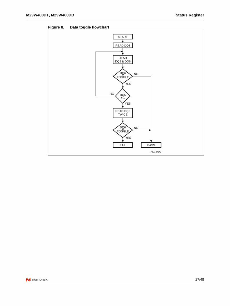
Figure 8: Data toggle flowchart, gives an example of how to use the Data Toggle bit.
M29W400DT, M29W400DB Status Register
25/48
5.3 Error bit (DQ5)
The Error bit can be used to identify errors detected by the Program/Erase controller. The Error bit is set to ’1’ when a Program, Block Erase or Chip Erase operation fails to write the correct data to the memory. If the Error bit is set a Read/Reset command must be issued before other commands are issued. The Error bit is output on DQ5 when the Status Register is read.
Note that the Program command cannot change a bit set to ’0’ back to ’1’ and attempting to do so will set DQ5 to ‘1’. A Bus Read operation to that address will show the bit is still ‘0’. One of the Erase commands must be used to set all the bits in a block or in the whole memory from ’0’ to ’1’
5.4 Erase Timer bit (DQ3)
The Erase Timer bit can be used to identify the start of Program/Erase controller operation during a Block Erase command. Once the Program/Erase controller starts erasing, the Erase Timer bit is set to ’1’. Before the Program/Erase controller starts the Erase Timer bit is set to ‘0’ and additional blocks to be erased may be written to the command interface. The Erase Timer bit is output on DQ3 when the Status Register is read.
5.5 Alternative Toggle bit (DQ2)
The Alternative Toggle bit can be used to monitor the Program/Erase controller during Erase operations. The Alternative Toggle bit is output on DQ2 when the Status Register is read.
During Chip Erase and Block Erase operations the Toggle bit changes from ’0’ to ’1’ to ’0’, etc., with successive Bus Read operations from addresses within the blocks being erased. A protected block is treated the same as a block not being erased. Once the operation completes the memory returns to Read mode.
During Erase Suspend the Alternative Toggle bit changes from ’0’ to ’1’ to ’0’, etc. with successive Bus Read operations from addresses within the blocks being erased. Bus Read operations to addresses within blocks not being erased will output the memory cell data as if in Read mode.
After an Erase operation that causes the Error bit to be set the Alternative Toggle bit can be used to identify which block or blocks have caused the error. The Alternative Toggle bit changes from ’0’ to ’1’ to ’0’, etc. with successive Bus Read operations from addresses within blocks that have not erased correctly. The Alternative Toggle bit does not change if the addressed block has erased correctly.
Table 7. Status Register bits(1)
Operation Address DQ7 DQ6 DQ5 DQ3 DQ2 RB
Program Any address DQ7 Toggle 0 – – 0
Program during Erase Suspend
Any address DQ7 Toggle 0 – – 0
Program Error Any address DQ7 Toggle 1 – – 0
Chip Erase Any address 0 Toggle 0 1 Toggle 0
Status Register M29W400DT, M29W400DB
26/48
Figure 7. Data polling flowchart
Block Erase before timeout
Erasing block 0 Toggle 0 0 Toggle 0
Non-erasing block
0 Toggle 0 0No
Toggle0
Block Erase
Erasing block 0 Toggle 0 1 Toggle 0
Non-erasing block
0 Toggle 0 1No
Toggle0
Erase Suspend
Erasing block 1No
Toggle0 – Toggle 1
Non-erasing block
Data read as normal 1
Erase Error
Good block address
0 Toggle 1 1No
Toggle0
Faulty block address
0 Toggle 1 1 Toggle 0
1. Unspecified data bits should be ignored.
Table 7. Status Register bits(1) (continued)
Operation Address DQ7 DQ6 DQ5 DQ3 DQ2 RB
READ DQ5 & DQ7at VALID ADDRESS
START
READ DQ7at VALID ADDRESS
FAIL PASS
AI03598
DQ7=
DATA
YES
NO
YES
NO
DQ5= 1
DQ7=
DATA
YES
NO
M29W400DT, M29W400DB Status Register
27/48
Figure 8. Data toggle flowchart
READ DQ6
START
READ DQ6TWICE
FAIL PASS
AI01370C
DQ6=
TOGGLENO
NO
YES
YES
DQ5= 1
NO
YES
DQ6=
TOGGLE
READDQ5 & DQ6
Maximum rating M29W400DT, M29W400DB
28/48
6 Maximum rating
Stressing the device above the rating listed in Table 8: Absolute maximum ratings may cause permanent damage to the device. Exposure to absolute maximum rating conditions for extended periods may affect device reliability. These are stress ratings only and operation of the device at these or any other conditions above those indicated in the operating sections of this specification is not implied. Refer also to the Numonyx SURE Program and other relevant quality documents.
Table 8. Absolute maximum ratings
Symbol Parameter Min Max Unit
TBIAS Temperature under bias –50 125 °C
TSTG Storage temperature –65 150 °C
TLEAD Lead temperature during soldering (1)
1. Compliant with the JEDEC Std J-STD-020B (for small body, Sn-Pb or Pb assermbly), the Numonyx RoHS specification, and the European directive on Restrictions on Hazardous Substances (RoHS) 2002/95/EU.
°C
VIO Input or output voltage(2)(3)
2. Minimum voltage may undershoot to –2 V during transition and for less than 20 ns during transitions.
3. Maximum voltage may overshoot to VCC+2 V during transition and for less than 20 ns during transitions.
–0.6 VCC+0.6 V
VCC Supply voltage –0.6 4 V
VID Identification voltage –0.6 13.5 V
M29W400DT, M29W400DB DC and AC parameters
29/48
7 DC and AC parameters
This section summarizes the operating measurement conditions, and the DC and AC characteristics of the device. The parameters in the DC and AC characteristics tables that follow, are derived from tests performed under the measurement conditions summarized in Table 9: Operating and AC measurement conditions. Designers should check that the operating conditions in their circuit match the operating conditions when relying on the quoted parameters.
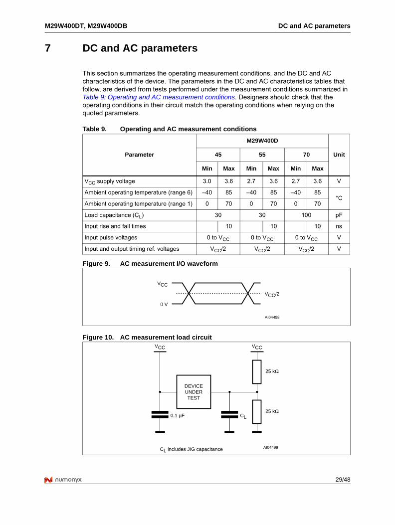
Figure 9. AC measurement I/O waveform
Figure 10. AC measurement load circuit
Table 9. Operating and AC measurement conditions
Parameter
M29W400D
Unit45 55 70
Min Max Min Max Min Max
VCC supply voltage 3.0 3.6 2.7 3.6 2.7 3.6 V
Ambient operating temperature (range 6) –40 85 –40 85 –40 85°C
Ambient operating temperature (range 1) 0 70 0 70 0 70
Load capacitance (CL) 30 30 100 pF
Input rise and fall times 10 10 10 ns
Input pulse voltages 0 to VCC 0 to VCC 0 to VCC V
Input and output timing ref. voltages VCC/2 VCC/2 VCC/2 V
AI04498
VCC
0 V
VCC/2
AI04499
CL
CL includes JIG capacitance
DEVICEUNDERTEST
25 kΩ
VCC
25 kΩ
VCC
0.1 µF
DC and AC parameters M29W400DT, M29W400DB
30/48
Figure 11. Read mode AC waveforms
Table 10. Device capacitance(1)
1. Sampled only, not 100% tested.
Symbol Parameter Test Condition Min Max Unit
CIN Input capacitance VIN = 0 V 6 pF
COUT Output capacitance VOUT = 0 V 12 pF
Table 11. DC characteristics
Symbol Parameter Test condition Min Max Unit
ILI Input Leakage current 0 V ≤ VIN ≤ VCC ±1 μA
ILO Output Leakage current 0 V ≤ VOUT ≤ VCC ±1 μA
ICC1 Supply current (Read)E = VIL, G = VIH,
f = 6 MHz10 mA
ICC2 Supply current (Standby)E = VCC ± 0.2 V,
RP = VCC ± 0.2 V100 μA
ICC3(1)
1. Sampled only, not 100% tested.
Supply current (Program/Erase)
Program/Erase controller active
20 mA
VIL Input Low voltage –0.5 0.8 V
VIH Input High voltage 0.7VCC VCC + 0.3 V
VOL Output Low voltage IOL = 1.8 mA 0.45 V
VOH Output High voltage IOH = –100 μA VCC – 0.4 V
VID Identification voltage 11.5 12.5 V
IID Identification current A9 = VID 100 μA
VLKOProgram/Erase Lockout supply voltage
1.8 2.3 V
AI02907
tAVAV
tAVQV tAXQX
tELQX tEHQZ
tGLQV
tGLQX tGHQX
VALID
A0-A17/A–1
G
DQ0-DQ7/DQ8-DQ15
E
tELQV tEHQX
tGHQZ
VALID
tBHQV
tELBL/tELBH tBLQZ
BYTE
M29W400DT, M29W400DB DC and AC parameters
31/48
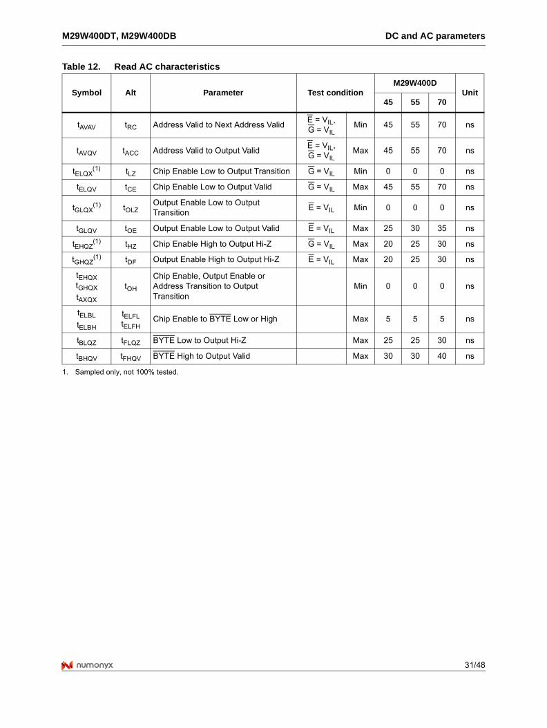
Table 12. Read AC characteristics
Symbol Alt Parameter Test conditionM29W400D
Unit45 55 70
tAVAV tRC Address Valid to Next Address ValidE = VIL,G = VIL
Min 45 55 70 ns
tAVQV tACC Address Valid to Output ValidE = VIL,G = VIL
Max 45 55 70 ns
tELQX(1) tLZ Chip Enable Low to Output Transition G = VIL Min 0 0 0 ns
tELQV tCE Chip Enable Low to Output Valid G = VIL Max 45 55 70 ns
tGLQX(1) tOLZ
Output Enable Low to Output Transition
E = VIL Min 0 0 0 ns
tGLQV tOE Output Enable Low to Output Valid E = VIL Max 25 30 35 ns
tEHQZ(1) tHZ Chip Enable High to Output Hi-Z G = VIL Max 20 25 30 ns
tGHQZ(1) tDF Output Enable High to Output Hi-Z E = VIL Max 20 25 30 ns
tEHQXtGHQX
tAXQX
tOH
Chip Enable, Output Enable or Address Transition to Output Transition
Min 0 0 0 ns
tELBL
tELBH
tELFLtELFH
Chip Enable to BYTE Low or High Max 5 5 5 ns
tBLQZ tFLQZ BYTE Low to Output Hi-Z Max 25 25 30 ns
tBHQV tFHQV BYTE High to Output Valid Max 30 30 40 ns
1. Sampled only, not 100% tested.
DC and AC parameters M29W400DT, M29W400DB
32/48
Figure 12. Write AC waveforms, Write Enable controlled
AI01869C
E
G
W
A0-A17/A–1
DQ0-DQ7/DQ8-DQ15
VALID
VALID
VCC
tVCHEL
tWHEH
tWHWL
tELWL
tAVWL
tWHGL
tWLAX
tWHDX
tAVAV
tDVWH
tWLWHtGHWL
RB
tWHRL
Table 13. Write AC characteristics, Write Enable controlled
Symbol Alt ParameterM29W400D
Unit45 55 70
tAVAV tWC Address Valid to Next Address Valid Min 45 55 70 ns
tELWL tCS Chip Enable Low to Write Enable Low Min 0 0 0 ns
tWLWH tWP Write Enable Low to Write Enable High Min 30 30 30 ns
tDVWH tDS Input Valid to Write Enable High Min 25 30 45 ns
tWHDX tDH Write Enable High to Input Transition Min 0 0 0 ns
tWHEH tCH Write Enable High to Chip Enable High Min 0 0 0 ns
tWHWL tWPH Write Enable High to Write Enable Low Min 30 30 30 ns
tAVWL tAS Address Valid to Write Enable Low Min 0 0 0 ns
tWLAX tAH Write Enable Low to Address Transition Min 40 45 45 ns
tGHWL Output Enable High to Write Enable Low Min 0 0 0 ns
tWHGL tOEH Write Enable High to Output Enable Low Min 0 0 0 ns
tWHRL(1) tBUSY Program/Erase Valid to RB Low Max 30 30 35 ns
tVCHEL tVCS VCC High to Chip Enable Low Min 50 50 50 μs
1. Sampled only, not 100% tested.
M29W400DT, M29W400DB DC and AC parameters
33/48
Figure 13. Write AC waveforms, Chip Enable controlled
AI01870C
E
G
W
A0-A17/A–1
DQ0-DQ7/DQ8-DQ15
VALID
VALID
VCC
tVCHWL
tEHWH
tEHEL
tWLEL
tAVEL
tEHGL
tELAX
tEHDX
tAVAV
tDVEH
tELEHtGHEL
RB
tEHRL
Table 14. Write AC characteristics, Chip Enable controlled
Symbol Alt ParameterM29W400D
Unit45 55 70
tAVAV tWC Address Valid to Next Address Valid Min 45 55 70 ns
tWLEL tWS Write Enable Low to Chip Enable Low Min 0 0 0 ns
tELEH tCP Chip Enable Low to Chip Enable High Min 30 30 30 ns
tDVEH tDS Input Valid to Chip Enable High Min 25 30 45 ns
tEHDX tDH Chip Enable High to Input Transition Min 0 0 0 ns
tEHWH tWH Chip Enable High to Write Enable High Min 0 0 0 ns
tEHEL tCPH Chip Enable High to Chip Enable Low Min 30 30 30 ns
tAVEL tAS Address Valid to Chip Enable Low Min 0 0 0 ns
tELAX tAH Chip Enable Low to Address Transition Min 40 45 45 ns
tGHEL Output Enable High Chip Enable Low Min 0 0 0 ns
tEHGL tOEH Chip Enable High to Output Enable Low Min 0 0 0 ns
tEHRL(1) tBUSY Program/Erase Valid to RB Low Max 30 30 35 ns
tVCHWL tVCS VCC High to Write Enable Low Min 50 50 50 μs
1. Sampled only, not 100% tested.
DC and AC parameters M29W400DT, M29W400DB
34/48
Figure 14. Reset/Block Temporary Unprotect AC waveforms
AI02931
RB
W,
RPtPLPX
tPHWL, tPHEL, tPHGL
tPLYH
tPHPHH
E, G
tRHWL, tRHEL, tRHGL
Table 15. Reset/Block Temporary Unprotect AC characteristics
Symbol Alt ParameterM29W400D
Unit45 55 70
tPHWL(1)
tPHEL
tPHGL(1)
tRHRP High to Write Enable Low, Chip Enable Low, Output Enable Low
Min 50 50 50 ns
tRHWL(1)
tRHEL(1)
tRHGL(1)
tRBRB High to Write Enable Low, Chip Enable Low, Output Enable Low
Min 0 0 0 ns
tPLPX tRP RP Pulse width Min 500 500 500 ns
tPLYH(1) tREADY RP Low to Read mode Max 10 10 10 μs
tPHPHH(1) tVIDR RP Rise time to VID Min 500 500 500 ns
1. Sampled only, not 100% tested.
M29W400DT, M29W400DB Package mechanical
35/48
8 Package mechanical
Figure 15. SO44 - 44 lead plastic small outline, 525 mils body width, package outline
1. Drawing is not to scale.
Table 16. SO44 – 44 lead plastic small outline, 525 mils body width, package mechanical data
Symbolmillimeters inches
Typ Min Max Typ Min Max
A 2.80 0.110
A1 0.10 0.004
A2 2.30 2.20 2.40 0.091 0.087 0.094
b 0.40 0.35 0.50 0.016 0.014 0.020
C 0.15 0.10 0.20 0.006 0.004 0.008
CP 0.08 0.003
D 28.20 28.00 28.40 1.110 1.102 1.118
E 13.30 13.20 13.50 0.524 0.520 0.531
EH 16.00 15.75 16.25 0.630 0.620 0.640
e 1.27 – – 0.050 – –
L 0.80 0.031
a 8 8
N 44 44
SO-d
E
N
D
C
LA1 α
EH
A
1
eCP
b
A2
Package mechanical M29W400DT, M29W400DB
36/48
Figure 16. TSOP48 – 48 lead plastic thin small outline, 12 x 20 mm, package outline
1. Drawing is not to scale.
Table 17. TSOP48 – 48 lead plastic thin small outline, 12 x 20 mm, package mechanical data
Symbolmillimeters inches
Typ Min Max Typ Min Max
A 1.20 0.047
A1 0.10 0.05 0.15 0.004 0.002 0.006
A2 1.00 0.95 1.05 0.039 0.037 0.041
B 0.22 0.17 0.27 0.009 0.007 0.011
C 0.10 0.21 0.004 0.008
CP 0.08 0.003
D1 12.00 11.90 12.10 0.472 0.468 0.476
E 20.00 19.80 20.20 0.787 0.779 0.795
E1 18.40 18.30 18.50 0.724 0.720 0.728
e 0.50 – – 0.020 – –
L 0.60 0.50 0.70 0.024 0.020 0.028
L1 0.80 0.031
a 3 0 5 3 0 5
TSOP-G
B
e
DIE
C
LA1 α
E1
E
AA2
1
24
48
25
D1
L1
CP
M29W400DT, M29W400DB Package mechanical
37/48
Figure 17. TFBGA48 6 x 9 mm, 6 x 8 active ball array, 0.80 mm pitch, bottom view package outline
1. Drawing is not to scale.
Table 18. TFBGA48 6 x 9 mm, 6 x 8 active ball array, 0.80 mm pitch, package mechanical data
Symbolmillimeters inches
Typ Min Max Typ Min Max
A 1.20 0.047
A1 0.20 0.008
A2 1.00 0.039
b 0.40 0.35 0.45 0.016 0.014 0.018
D 6.00 5.90 6.10 0.236 0.232 0.240
D1 4.00 – – 0.157 – –
ddd 0.10 0.004
E 9.00 8.90 9.10 0.354 0.350 0.358
e 0.80 – – 0.031 – –
E1 5.60 – – 0.220 – –
FD 1.00 – – 0.039 – –
FE 1.70 – – 0.067 – –
SD 0.40 – – 0.016 – –
SE 0.40 – – 0.016 – –
E1E
D1
D
e bA2
A1A
BGA-Z00
ddd
FD
FE SD
SE
e
BALL "A1"
Package mechanical M29W400DT, M29W400DB
38/48
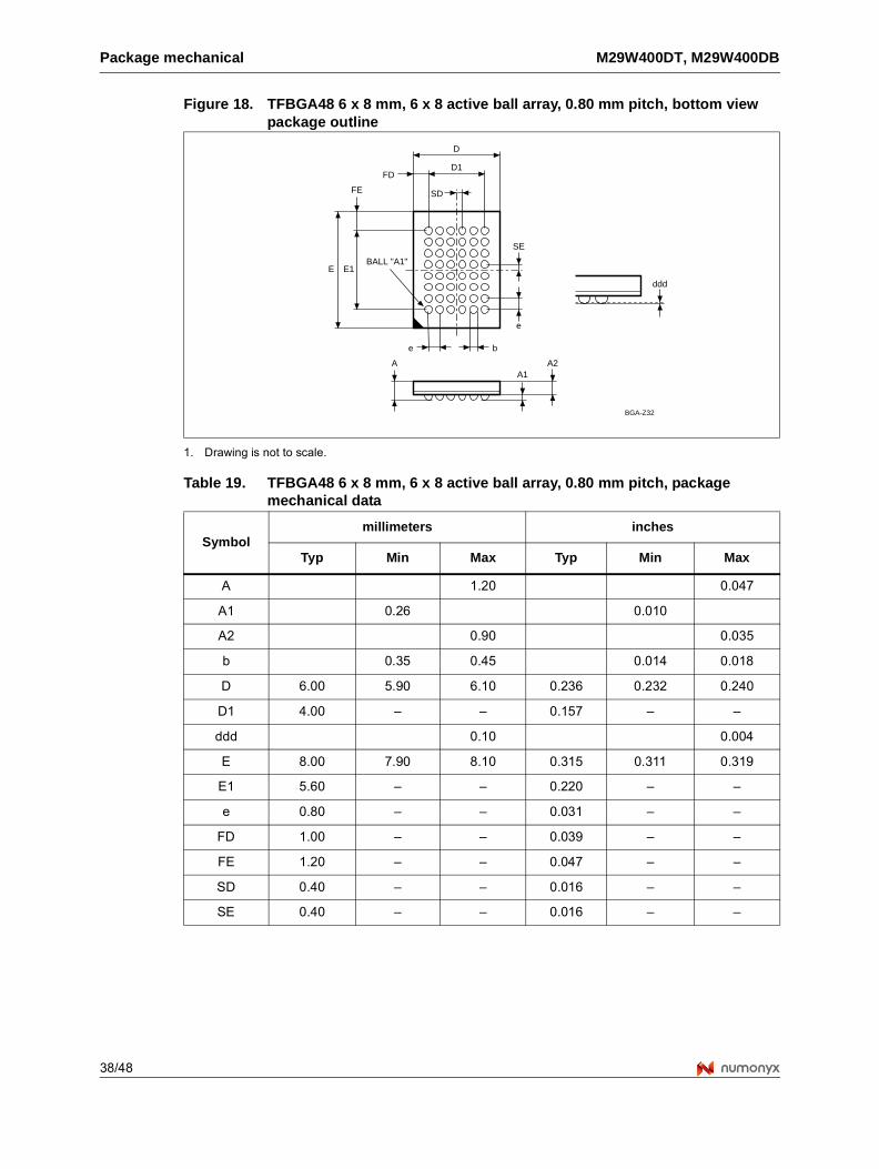
Figure 18. TFBGA48 6 x 8 mm, 6 x 8 active ball array, 0.80 mm pitch, bottom view package outline
1. Drawing is not to scale.
Table 19. TFBGA48 6 x 8 mm, 6 x 8 active ball array, 0.80 mm pitch, package mechanical data
Symbolmillimeters inches
Typ Min Max Typ Min Max
A 1.20 0.047
A1 0.26 0.010
A2 0.90 0.035
b 0.35 0.45 0.014 0.018
D 6.00 5.90 6.10 0.236 0.232 0.240
D1 4.00 – – 0.157 – –
ddd 0.10 0.004
E 8.00 7.90 8.10 0.315 0.311 0.319
E1 5.60 – – 0.220 – –
e 0.80 – – 0.031 – –
FD 1.00 – – 0.039 – –
FE 1.20 – – 0.047 – –
SD 0.40 – – 0.016 – –
SE 0.40 – – 0.016 – –
E1E
D1
D
e b
A2A1
A
BGA-Z32
ddd
FD
FE SD
SE
e
BALL "A1"
M29W400DT, M29W400DB Part numbering
39/48
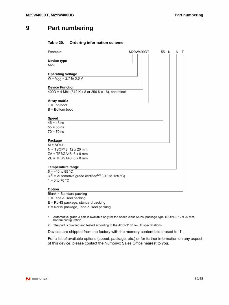
9 Part numbering
Table 20. Ordering information scheme
Devices are shipped from the factory with the memory content bits erased to ’1’.
For a list of available options (speed, package, etc.) or for further information on any aspect of this device, please contact the Numonyx Sales Office nearest to you.
Example: M29W400DT 55 N 6 T
Device typeM29
Operating voltageW = VCC = 2.7 to 3.6 V
Device Function400D = 4 Mbit (512 K x 8 or 256 K x 16), boot block
Array matrixT = Top bootB = Bottom boot
Speed45 = 45 ns55 = 55 ns70 = 70 ns
PackageM = SO44N = TSOP48: 12 x 20 mmZA = TFBGA48: 6 x 9 mmZE = TFBGA48: 6 x 8 mm
Temperature range6 = –40 to 85 °C3(1) = Automotive grade certified(2) (–40 to 125 °C)
1. Automotive grade 3 part is available only for the speed class 55 ns, package type TSOP48, 12 x 20 mm, bottom configuration.
2. The part is qualfied and tested according to the AEC-Q100 rev. G specifications.
1 = 0 to 70 °C
OptionBlank = Standard packingT = Tape & Reel packingE = RoHS package, standard packingF = RoHS package, Tape & Reel packing
Block address table M29W400DT, M29W400DB
40/48
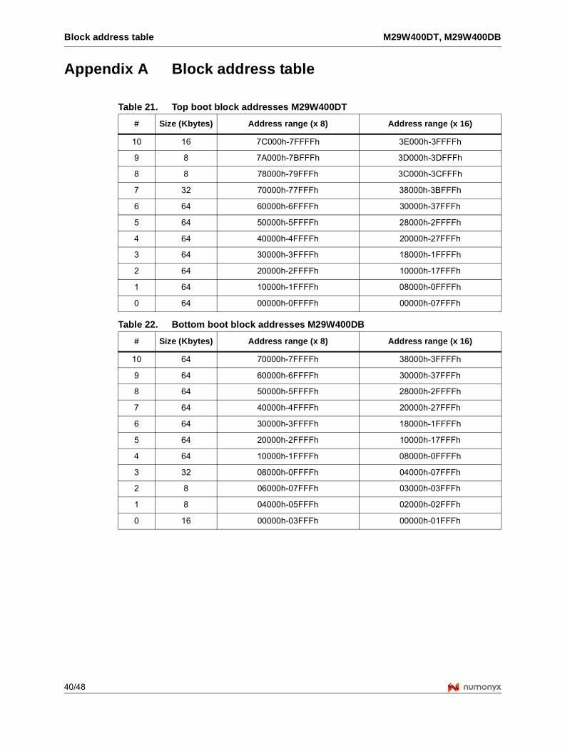
Appendix A Block address table
Table 21. Top boot block addresses M29W400DT
# Size (Kbytes) Address range (x 8) Address range (x 16)
10 16 7C000h-7FFFFh 3E000h-3FFFFh
9 8 7A000h-7BFFFh 3D000h-3DFFFh
8 8 78000h-79FFFh 3C000h-3CFFFh
7 32 70000h-77FFFh 38000h-3BFFFh
6 64 60000h-6FFFFh 30000h-37FFFh
5 64 50000h-5FFFFh 28000h-2FFFFh
4 64 40000h-4FFFFh 20000h-27FFFh
3 64 30000h-3FFFFh 18000h-1FFFFh
2 64 20000h-2FFFFh 10000h-17FFFh
1 64 10000h-1FFFFh 08000h-0FFFFh
0 64 00000h-0FFFFh 00000h-07FFFh
Table 22. Bottom boot block addresses M29W400DB
# Size (Kbytes) Address range (x 8) Address range (x 16)
10 64 70000h-7FFFFh 38000h-3FFFFh
9 64 60000h-6FFFFh 30000h-37FFFh
8 64 50000h-5FFFFh 28000h-2FFFFh
7 64 40000h-4FFFFh 20000h-27FFFh
6 64 30000h-3FFFFh 18000h-1FFFFh
5 64 20000h-2FFFFh 10000h-17FFFh
4 64 10000h-1FFFFh 08000h-0FFFFh
3 32 08000h-0FFFFh 04000h-07FFFh
2 8 06000h-07FFFh 03000h-03FFFh
1 8 04000h-05FFFh 02000h-02FFFh
0 16 00000h-03FFFh 00000h-01FFFh
M29W400DT, M29W400DB Block protection
41/48
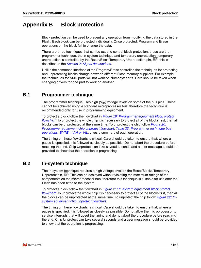
Appendix B Block protection
Block protection can be used to prevent any operation from modifying the data stored in the Flash. Each block can be protected individually. Once protected, Program and Erase operations on the block fail to change the data.
There are three techniques that can be used to control block protection, these are the programmer technique, the in-system technique and temporary unprotection. temporary unprotection is controlled by the Reset/Block Temporary Unprotection pin, RP; this is described in the Section 2: Signal descriptions.
Unlike the command interface of the Program/Erase controller, the techniques for protecting and unprotecting blocks change between different Flash memory suppliers. For example, the techniques for AMD parts will not work on Numonyx parts. Care should be taken when changing drivers for one part to work on another.
B.1 Programmer technique
The programmer technique uses high (VID) voltage levels on some of the bus pins. These cannot be achieved using a standard microprocessor bus, therefore the technique is recommended only for use in programming equipment.
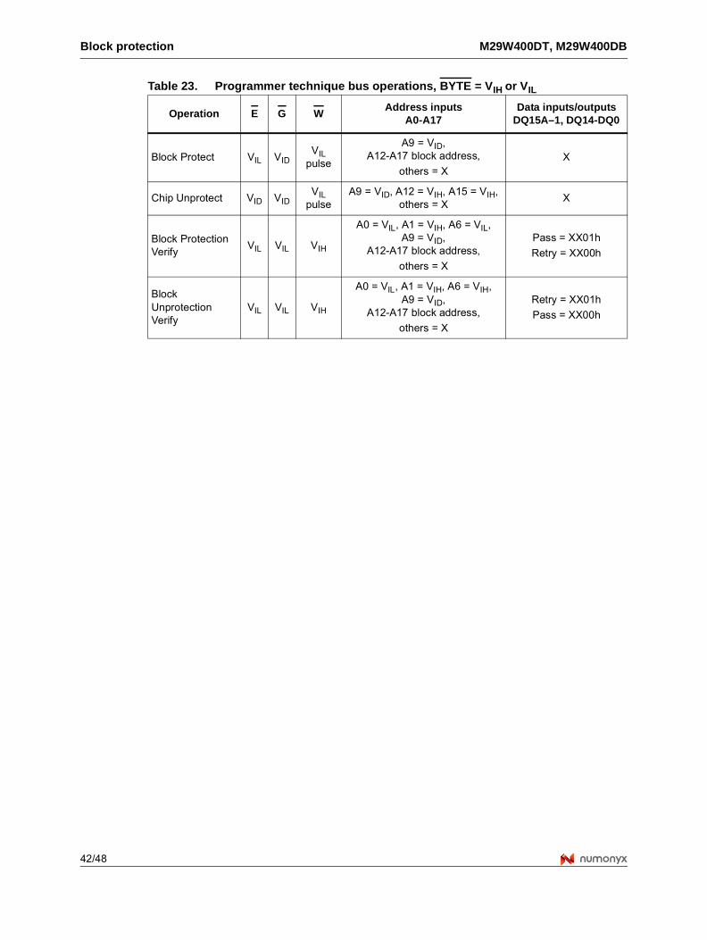
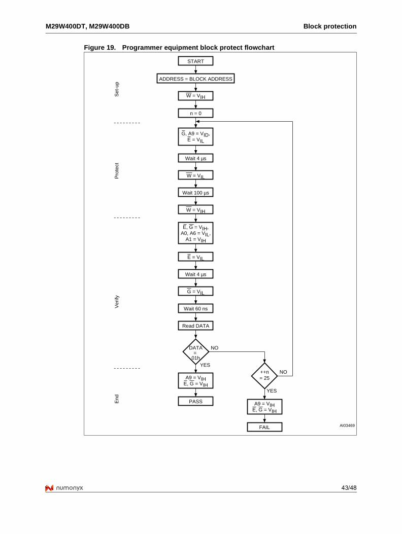
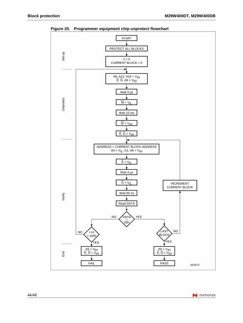
To protect a block follow the flowchart in Figure 19: Programmer equipment block protect flowchart. To unprotect the whole chip it is necessary to protect all of the blocks first, then all blocks can be unprotected at the same time. To unprotect the chip follow Figure 20: Programmer equipment chip unprotect flowchart. Table 23: Programmer technique bus operations, BYTE = VIH or VIL, gives a summary of each operation.
The timing on these flowcharts is critical. Care should be taken to ensure that, where a pause is specified, it is followed as closely as possible. Do not abort the procedure before reaching the end. Chip Unprotect can take several seconds and a user message should be provided to show that the operation is progressing.
B.2 In-system technique
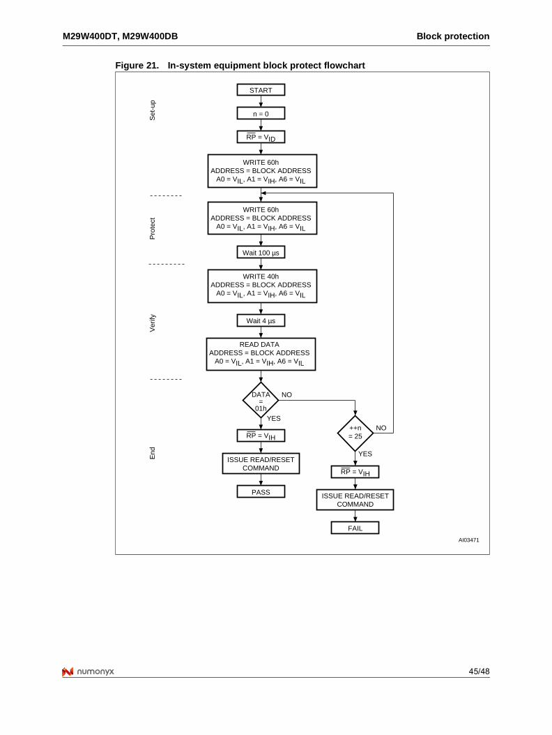
The in-system technique requires a high voltage level on the Reset/Blocks Temporary Unprotect pin, RP. This can be achieved without violating the maximum ratings of the components on the microprocessor bus, therefore this technique is suitable for use after the Flash has been fitted to the system.
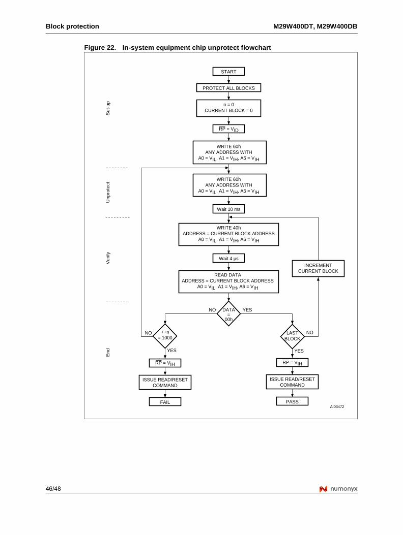
To protect a block follow the flowchart in Figure 21: In-system equipment block protect flowchart. To unprotect the whole chip it is necessary to protect all of the blocks first, then all the blocks can be unprotected at the same time. To unprotect the chip follow Figure 22: In-system equipment chip unprotect flowchart.
The timing on these flowcharts is critical. Care should be taken to ensure that, where a pause is specified, it is followed as closely as possible. Do not allow the microprocessor to service interrupts that will upset the timing and do not abort the procedure before reaching the end. Chip Unprotect can take several seconds and a user message should be provided to show that the operation is progressing.
Block protection M29W400DT, M29W400DB
42/48
Table 23. Programmer technique bus operations, BYTE = VIH or VIL
Operation E G WAddress inputs
A0-A17Data inputs/outputs
DQ15A–1, DQ14-DQ0
Block Protect VIL VIDVIL
pulse
A9 = VID,A12-A17 block address,
others = XX
Chip Unprotect VID VIDVIL
pulseA9 = VID, A12 = VIH, A15 = VIH,
others = XX
Block Protection Verify
VIL VIL VIH
A0 = VIL, A1 = VIH, A6 = VIL, A9 = VID,
A12-A17 block address,
others = X
Pass = XX01h
Retry = XX00h
Block Unprotection Verify
VIL VIL VIH
A0 = VIL, A1 = VIH, A6 = VIH, A9 = VID,
A12-A17 block address,
others = X
Retry = XX01h
Pass = XX00h
M29W400DT, M29W400DB Block protection
43/48
Figure 19. Programmer equipment block protect flowchart
ADDRESS = BLOCK ADDRESS
AI03469
G, A9 = VID,E = VIL
n = 0
Wait 4 µs
Wait 100 µs
W = VIL
W = VIH
E, G = VIH,A0, A6 = VIL,
A1 = VIH
A9 = VIHE, G = VIH
++n= 25
START
FAIL
PASS
YES
NO
DATA=
01hYES
NO
W = VIH
E = VIL
Wait 4 µs
G = VIL
Wait 60 ns
Read DATA
Ver
ifyP
rote
ctS
et-u
pE
nd
A9 = VIHE, G = VIH
Block protection M29W400DT, M29W400DB
44/48
Figure 20. Programmer equipment chip unprotect flowchart
PROTECT ALL BLOCKS
AI03470
A6, A12, A15 = VIHE, G, A9 = VID
DATA
W = VIH
E, G = VIH
ADDRESS = CURRENT BLOCK ADDRESSA0 = VIL, A1, A6 = VIH
Wait 10 ms
=00h
INCREMENTCURRENT BLOCK
n = 0CURRENT BLOCK = 0
Wait 4 µs
W = VIL
++n= 1000
START
YES
YESNO
NO LASTBLOCK
YES
NO
E = VIL
Wait 4 µs
G = VIL
Wait 60 ns
Read DATA
FAIL PASS
Ver
ifyU
npro
tect
Set
-up
End
A9 = VIHE, G = VIH
A9 = VIHE, G = VIH
M29W400DT, M29W400DB Block protection
45/48
Figure 21. In-system equipment block protect flowchart
AI03471
WRITE 60hADDRESS = BLOCK ADDRESS
A0 = VIL, A1 = VIH, A6 = VIL
n = 0
Wait 100 µs
WRITE 40hADDRESS = BLOCK ADDRESS
A0 = VIL, A1 = VIH, A6 = VIL
RP = VIH++n= 25
START
FAIL
PASS
YES
NO
DATA=
01hYES
NO
RP = VIH
Wait 4 µs
Ver
ifyP
rote
ctS
et-u
pE
nd
READ DATAADDRESS = BLOCK ADDRESS
A0 = VIL, A1 = VIH, A6 = VIL
RP = VID
ISSUE READ/RESETCOMMAND
ISSUE READ/RESETCOMMAND
WRITE 60hADDRESS = BLOCK ADDRESS
A0 = VIL, A1 = VIH, A6 = VIL
Block protection M29W400DT, M29W400DB
46/48
Figure 22. In-system equipment chip unprotect flowchart
AI03472
WRITE 60hANY ADDRESS WITH
A0 = VIL, A1 = VIH, A6 = VIH
n = 0CURRENT BLOCK = 0
Wait 10 ms
WRITE 40hADDRESS = CURRENT BLOCK ADDRESS
A0 = VIL, A1 = VIH, A6 = VIH
RP = VIH
++n= 1000
START
FAIL PASS
YES
NO
DATA=
00h
YESNO
RP = VIH
Wait 4 µs
READ DATAADDRESS = CURRENT BLOCK ADDRESS
A0 = VIL, A1 = VIH, A6 = VIH
RP = VID
ISSUE READ/RESETCOMMAND
ISSUE READ/RESETCOMMAND
PROTECT ALL BLOCKS
INCREMENTCURRENT BLOCK
LASTBLOCK
YES
NO
WRITE 60hANY ADDRESS WITH
A0 = VIL, A1 = VIH, A6 = VIH
Ver
ifyU
npro
tect
Set
-up
End
M29W400DT, M29W400DB Revision history
10 Revision history
Table 24. Document revision history
Date Revision Changes
26-Jul-2002 01 Initial release
19-Feb-2003 2.0
Revision numbering modified: a minor revision will be indicated by incrementing the digit after the dot, and a major revision, by incrementing the digit before the dot (revision version 01 equals 1.0). Revision history moved to end of document. Typical after 100k W/E cycles column removed from Table 4: Program, Erase times and Program, Erase endurance cycles, Data retention and Erase Suspend latency time parameters added. Common Flash interface removed from datasheet. Lead-free package options E and F added to Table 20: Ordering information scheme. Document promoted from Product Preview to Preliminary Data status.
28-May-2003 2.1
tWLWH and tELEH parameters modified for all speed classes in Table 13: Write AC characteristics, Write Enable controlled and Table 14: Write AC characteristics, Chip Enable controlled. Minor text changes. TSOP48 package updated (Figure 16 and Table 17).
30-Sep-2003 2.2 Document status changed to Full datasheet. TFBGA48 6 x 8 package added. TLEAD parameter added in Table 8: Absolute maximum ratings.
6-Oct-2003 2.3 tGLQV modified in Table 12: Read AC characteristics.
16-Jan-2004 3 RB pin description corrected in Table : .
8-Jun-2004 4 Tape and Reel option updated in Table 20: Ordering information scheme. Lead-free packaging promotion updated in Section 1: Description, Section 6: Maximum rating and Section 9: Part numbering.
07-Aug-2007 5 RoHS text added in Section 1: Description. Updated options E and F in Table 20: Ordering information scheme. Small text changes.
10-Dec-2007 6 Applied Numonyx branding.
2-March 2009 7 Added Automotive Grade 3 part information to cover page and part ordering information.
7-April-2009 8
Revised BYTE signal name from “output” to “input” in Table 1.: Signal names; Revised Chip Erase signal value (maximum) in Table 4.: Program, Erase times and Program, Erase endurance cycles from 35 to 12 seconds. Revised Block Erase (64-Kbytes) signal value (maximum) in Table 4.: Program, Erase times and Program, Erase endurance cycles from 6 to 1.6 seconds.
29-Jan 2018 9 Added Important Notes and Warnings section for further clarification aligning to industry standards.
47/48

M29W400DT, M29W400DB
48/48