LTM8078 (Rev. 0) - Mouser
24
LTM8078 1 Rev. 0 For more information www.analog.com TYPICAL APPLICATION FEATURES DESCRIPTION Dual 1.4A, Single 2.8A Step-Down Silent Switcher μModule Regulator The LTM ® 8078 is 40V IN, dual 1.4A/single 2.8A step-down Silent Switcher μModule ® regulator. The Silent Switcher architecture minimizes EMI while delivering high efficiency at frequencies up to 3MHz. Included in the package are the controllers, power switches, inductors, and support com- ponents. Operating over a wide input voltage range, the LTM8078 supports output voltages from 0.8V to 10V, and a switching frequency range of 300kHz to 3MHz, each set by a single resistor. Only the bulk input and output filter capacitors are needed to finish the design. The LTM8078 product video is available on website. The LTM8078 is packaged in a compact (6.25mm × 6.25mm × 2.22mm) over-molded Ball Grid Array (BGA) package suitable for automated assembly by standard surface mount equipment. The LTM8078 is available with SnPb (BGA) or RoHS compliant. 3.3V OUT and 5V OUT from 7V to 40V Dual Step-Down Converter APPLICATIONS n Two Complete Step-Down Switching Power Supplies n Low Noise Silent Switcher ® Architecture n CISPR22 Class B Compliant n Wide Input Voltage Range: 3V to 40V n Wide Output Voltage Range: 0.8V to 10V n 1.4A Continuous Output Current per Channel at 24V IN , 3.3V OUT , T A = 85°C n Multiphase Parallel Operation to Increase Current n Selectable Switching Frequency: 300kHz to 3MHz n Compact Package (6.25mm × 6.25mm × 2.22mm) Surface Mount BGA n Automated Test Equipment n Distributed Supply Regulation n Industrial Supplies n Medical Equipment All registered trademarks and trademarks are the property of their respective owners. Efficiency, V IN = 24V, BIAS = 5V Document Feedback 1μF 17.8k 47.5k 47 μF 78.7k 100μF 1μF V IN1 RUN V OUT1 FB1 RT V IN2 V OUT2 FB2 GND BIAS (1.6MHz) V OUT2 5V 1.4A V OUT1 3.3V 1.4A V IN 7V TO 40V PINS NOT USED: TRSS1, TRSS2, PG1, PG2, CLKOUT, SYNC OM OMC 8078 TA01a LTM8078 3.3V OUT 5.0V OUT LOAD CURRENT (A) 0 0.5 1 1.5 2 2.5 75 80 85 90 95 EFFICIENCY (%) 8078 TA01b T A = 25°C Click to view associated Video Design Idea.
Transcript of LTM8078 (Rev. 0) - Mouser
LTM8078
1Rev. 0
For more information www.analog.com
TYPICAL APPLICATION
FEATURES DESCRIPTION
Dual 1.4A, Single 2.8A Step-Down Silent Switcher μModule Regulator
The LTM®8078 is 40VIN, dual 1.4A/single 2.8A step-down Silent Switcher μModule® regulator. The Silent Switcher architecture minimizes EMI while delivering high efficiency at frequencies up to 3MHz. Included in the package are the controllers, power switches, inductors, and support com-ponents. Operating over a wide input voltage range, the LTM8078 supports output voltages from 0.8V to 10V, and a switching frequency range of 300kHz to 3MHz, each set by a single resistor. Only the bulk input and output filter capacitors are needed to finish the design. The LTM8078 product video is available on website.
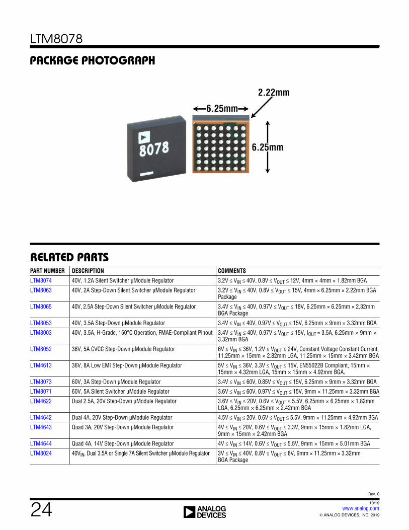
The LTM8078 is packaged in a compact (6.25mm × 6.25mm × 2.22mm) over-molded Ball Grid Array (BGA) package suitable for automated assembly by standard surface mount equipment. The LTM8078 is available with SnPb (BGA) or RoHS compliant.
3.3VOUT and 5VOUT from 7V to 40V Dual Step-Down Converter
APPLICATIONS
n Two Complete Step-Down Switching Power Supplies n Low Noise Silent Switcher® Architecture n CISPR22 Class B Compliant n Wide Input Voltage Range: 3V to 40V n Wide Output Voltage Range: 0.8V to 10V n 1.4A Continuous Output Current per Channel at
24VIN, 3.3VOUT, TA = 85°C n Multiphase Parallel Operation to Increase Current n Selectable Switching Frequency: 300kHz to 3MHz n Compact Package (6.25mm × 6.25mm × 2.22mm)
Surface Mount BGA
n Automated Test Equipment n Distributed Supply Regulation n Industrial Supplies n Medical Equipment All registered trademarks and trademarks are the property of their respective owners.
Efficiency, VIN = 24V, BIAS = 5V
Document Feedback
1µF
17.8k
47.5k47 µF
78.7k100µF
1µF
VIN1
RUN
VOUT1
FB1
RT
VIN2
VOUT2
FB2
GND
BIAS
(1.6MHz)
VOUT25V1.4A
VOUT13.3V1.4A
VIN7V TO 40V
PINS NOT USED: TRSS1, TRSS2, PG1, PG2, CLKOUT, SYNC
OM
OMC
8078 TA01a
LTM8078
3.3VOUT5.0VOUT
LOAD CURRENT (A)0 0.5 1 1.5 2 2.5
75
80
85
90
95
EFFI
CIEN
CY (%
)
Efficiency, VIN = 24V, BIAS = 5V
8078 TA01b
TA = 25°C
Click to view associated Video Design Idea.
LTM8078
2Rev. 0
For more information www.analog.com
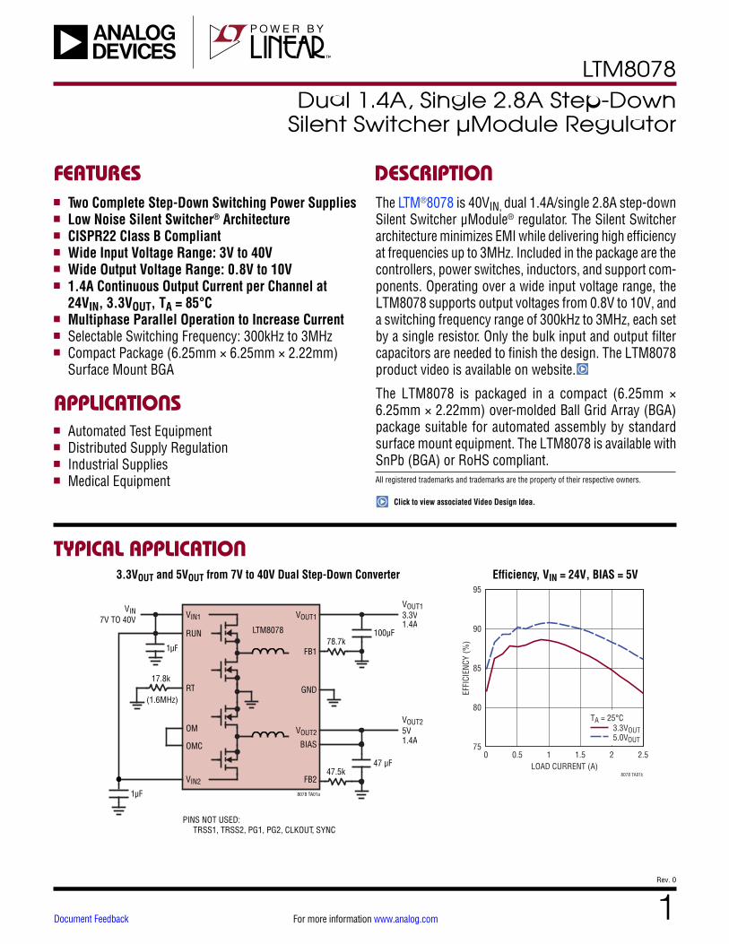
PIN CONFIGURATIONABSOLUTE MAXIMUM RATINGS
VINn, RUN, PGn ........................................................42VVOUTn, BIAS .............................................................10VFBn, OM, OMC, TRSSn, RT ........................................4VSYNC ..........................................................................6VMaximum Internal Temperature (Note 2) .............. 125°CStorage Temperature ............................. –55°C to 125°CPeak Solder Reflow Package Body Temperature .. 260°C
(Note 1)
VOUT2
BGA PACKAGE49-PIN (6.25mm × 6.25mm × 2.22mm)
TJMAX = 125°C, θJA = 31.3°C/W, θJCtop = 30.5°C/W, θJCbot = 10.6°C/W, WEIGHT = 0.23g
θ VALUES DETERMINED PER JESD 51-9, 51-12
VIN2
RT
BANK 2
BANK 1
GND
VOUT1
VIN1
PG2
GND
PG1 SYNC CLKOUT
7
6
5
4
3
2
1
A B C D E F G
TRSS2 TRSS1 OM OMC
RUN
BIASFB1FB2
BANK 3
ORDER INFORMATION
PART NUMBER PAD OR BALL FINISH
PART MARKING PACKAGE TYPE
MSL RATING
TEMPERATURE RANGE (SEE NOTE 2)DEVICE FINISH CODE
LTM8078EY#PBFSAC305 (RoHS) 8078 1 BGA 3 –40°C to 125°C
LTM8078IY#PBF
• Device temperature grade is indicated by a label on the shipping container.
• Pad or ball finish code is per IPC/JEDEC J-STD-609.• BGA Package and Tray Drawings
• This product is not recommended for second side reflow. This product is moisture sensitive. For more information, go to Recommended BGA PCB Assembly and Manufacturing Procedures.
LTM8078
3Rev. 0
For more information www.analog.com
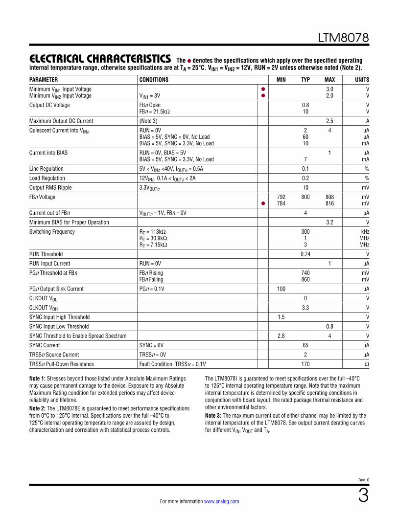
ELECTRICAL CHARACTERISTICS
Note 1: Stresses beyond those listed under Absolute Maximum Ratings may cause permanent damage to the device. Exposure to any Absolute Maximum Rating condition for extended periods may affect device reliability and lifetime.Note 2: The LTM8078E is guaranteed to meet performance specifications from 0°C to 125°C internal. Specifications over the full –40°C to 125°C internal operating temperature range are assured by design, characterization and correlation with statistical process controls.
The l denotes the specifications which apply over the specified operating internal temperature range, otherwise specifications are at TA = 25°C. VIN1 = VIN2 = 12V, RUN = 2V unless otherwise noted (Note 2).
PARAMETER CONDITIONS MIN TYP MAX UNITS
Minimum VIN1 Input Voltage Minimum VIN2 Input Voltage
VIN1 = 3V
l
l
3.0 2.0
V V
Output DC Voltage FBn Open FBn = 21.5kΩ
0.8 10
V V
Maximum Output DC Current (Note 3) 2.5 A
Quiescent Current into VINn RUN = 0V BIAS = 5V, SYNC = 0V, No Load BIAS = 5V, SYNC = 3.3V, No Load
2 60 10
4 μA µA
mA
Current into BIAS RUN = 0V, BIAS = 5V BIAS = 5V, SYNC = 3.3V, No Load
7
1 μA mA
Line Regulation 5V < VINn <40V, IOUTn = 0.5A 0.1 %
Load Regulation 12VINn, 0.1A < IOUTn < 2A 0.2 %
Output RMS Ripple 3.3VOUTn 10 mV
FBn Voltage
l
792 784
800 808 816
mV mV
Current out of FBn VOUTn = 1V, FBn = 0V 4 µA
Minimum BIAS for Proper Operation 3.2 V
Switching Frequency RT = 113kΩ RT = 30.9kΩ RT = 7.15kΩ
300 1 3
kHz MHz MHz
RUN Threshold 0.74 V
RUN Input Current RUN = 0V 1 μA
PGn Threshold at FBn FBn Rising FBn Falling
740 860
mV mV
PGn Output Sink Current PGn = 0.1V 100 μA
CLKOUT VOL 0 V
CLKOUT VOH 3.3 V
SYNC Input High Threshold 1.5 V
SYNC Input Low Threshold 0.8 V
SYNC Threshold to Enable Spread Spectrum 2.8 4 V
SYNC Current SYNC = 6V 65 μA
TRSSn Source Current TRSSn = 0V 2 μA
TRSSn Pull-Down Resistance Fault Condition, TRSSn = 0.1V 170 Ω
The LTM8078I is guaranteed to meet specifications over the full –40°C to 125°C internal operating temperature range. Note that the maximum internal temperature is determined by specific operating conditions in conjunction with board layout, the rated package thermal resistance and other environmental factors. Note 3: The maximum current out of either channel may be limited by the internal temperature of the LTM8078. See output current derating curves for different VIN, VOUT and TA.
LTM8078
4Rev. 0
For more information www.analog.com
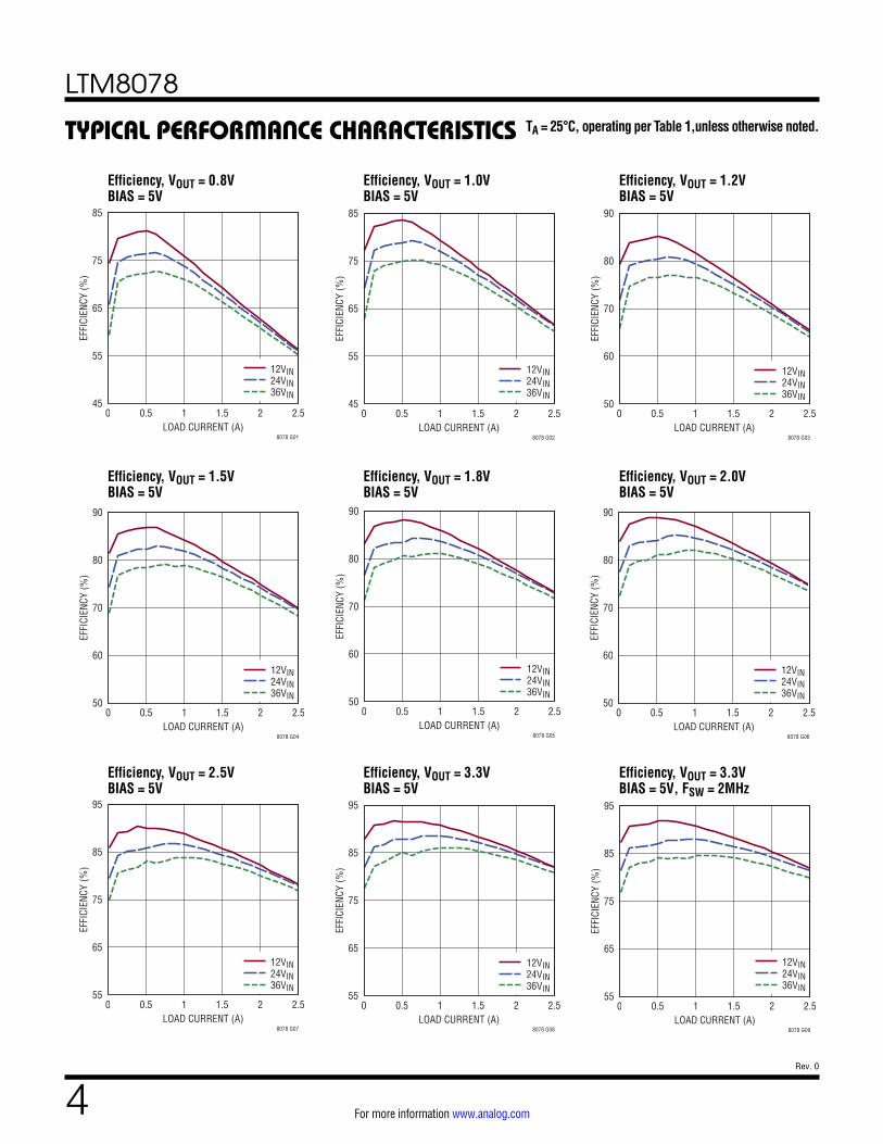
TA = 25°C, operating per Table 1,unless otherwise noted.TYPICAL PERFORMANCE CHARACTERISTICS
Efficiency, VOUT = 0.8V BIAS = 5V
Efficiency, VOUT = 1.0V BIAS = 5V
Efficiency, VOUT = 1.2V BIAS = 5V
Efficiency, VOUT = 1.5V BIAS = 5V
Efficiency, VOUT = 1.8V BIAS = 5V
Efficiency, VOUT = 2.0V BIAS = 5V
Efficiency, VOUT = 2.5V BIAS = 5V
Efficiency, VOUT = 3.3V BIAS = 5V
Efficiency, VOUT = 3.3V BIAS = 5V, FSW = 2MHz
12VIN24VIN36VIN
LOAD CURRENT (A)0 0.5 1 1.5 2 2.5
45
55
65
75
85
EFFI
CIEN
CY (%
)
BIAS = 5V
8078 G01
12VIN24VIN36VIN
LOAD CURRENT (A)0 0.5 1 1.5 2 2.5
45
55
65
75
85
EFFI
CIEN
CY (%
)
BIAS = 5V
8078 G02
12VIN24VIN36VIN
LOAD CURRENT (A)0 0.5 1 1.5 2 2.5
50
60
70
80
90
EFFI
CIEN
CY (%
)
BIAS = 5V
8078 G03
12VIN24VIN36VIN
LOAD CURRENT (A)0 0.5 1 1.5 2 2.5
50
60
70
80
90
EFFI
CIEN
CY (%
)
BIAS = 5V
8078 G04
12VIN24VIN36VIN
LOAD CURRENT (A)0 0.5 1 1.5 2 2.5
50
60
70
80
90
EFFI
CIEN
CY (%
)
BIAS = 5V
8078 G05
12VIN24VIN36VIN
LOAD CURRENT (A)0 0.5 1 1.5 2 2.5
50
60
70
80
90
EFFI
CIEN
CY (%
)
BIAS = 5V
8078 G06
12VIN24VIN36VIN
LOAD CURRENT (A)0 0.5 1 1.5 2 2.5
55
65
75
85
95
EFFI
CIEN
CY (%
)
BIAS = 5V
8078 G07
12VIN24VIN36VIN
LOAD CURRENT (A)0 0.5 1 1.5 2 2.5
55
65
75
85
95
EFFI
CIEN
CY (%
)
BIAS = 5V
8078 G08
12VIN24VIN36VIN
LOAD CURRENT (A)0 0.5 1 1.5 2 2.5
55
65
75
85
95
EFFI
CIEN
CY (%
)
SW
8078 G09
LTM8078
5Rev. 0
For more information www.analog.com
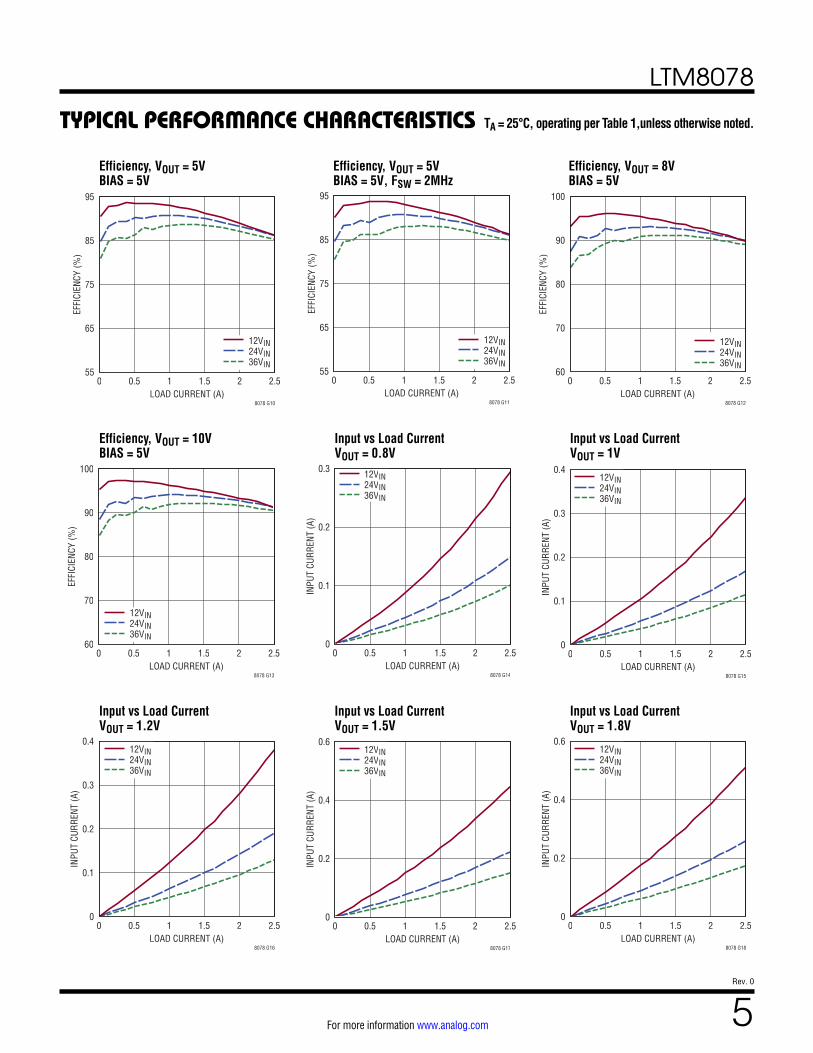
Efficiency, VOUT = 5V BIAS = 5V
Efficiency, VOUT = 5V BIAS = 5V, FSW = 2MHz
Efficiency, VOUT = 8V BIAS = 5V
Efficiency, VOUT = 10V BIAS = 5V
Input vs Load Current VOUT = 0.8V
Input vs Load Current VOUT = 1V
Input vs Load Current VOUT = 1.2V
Input vs Load Current VOUT = 1.5V
Input vs Load Current VOUT = 1.8V
TA = 25°C, operating per Table 1,unless otherwise noted.TYPICAL PERFORMANCE CHARACTERISTICS
12VIN24VIN36VIN
LOAD CURRENT (A)0 0.5 1 1.5 2 2.5
55
65
75
85
95
EFFI
CIEN
CY (%
)
BIAS = 5V
8078 G10
12VIN24VIN36VIN
LOAD CURRENT (A)0 0.5 1 1.5 2 2.5
55
65
75
85
95
EFFI
CIEN
CY (%
)
SW
8078 G11
12VIN24VIN36VIN
LOAD CURRENT (A)0 0.5 1 1.5 2 2.5
60
70
80
90
100
EFFI
CIEN
CY (%
)
8078 G12
12VIN24VIN36VIN
LOAD CURRENT (A)0 0.5 1 1.5 2 2.5
60
70
80
90
100
EFFI
CIEN
CY (%
)
BIAS = 5V
8078 G13
12VIN24VIN36VIN
LOAD CURRENT (A)0 0.5 1 1.5 2 2.5
0
0.1
0.2
0.3
INPU
T CU
RREN
T (A
)
OUT
8078 G14
12VIN24VIN36VIN
LOAD CURRENT (A)0 0.5 1 1.5 2 2.5
0
0.1
0.2
0.3
0.4
INPU
T CU
RREN
T (A
)
VOUT = 1.0V
8078 G15
12VIN24VIN36VIN
LOAD CURRENT (A)0 0.5 1 1.5 2 2.5
0
0.1
0.2
0.3
0.4
INPU
T CU
RREN
T (A
)
OUT
8078 G16
12VIN24VIN36VIN
LOAD CURRENT (A)0 0.5 1 1.5 2 2.5
0
0.2
0.4
0.6
INPU
T CU
RREN
T (A
)
OUT
8078 G17
12VIN24VIN36VIN
LOAD CURRENT (A)0 0.5 1 1.5 2 2.5
0
0.2
0.4
0.6
INPU
T CU
RREN
T (A
)
OUT
8078 G18
LTM8078
6Rev. 0
For more information www.analog.com
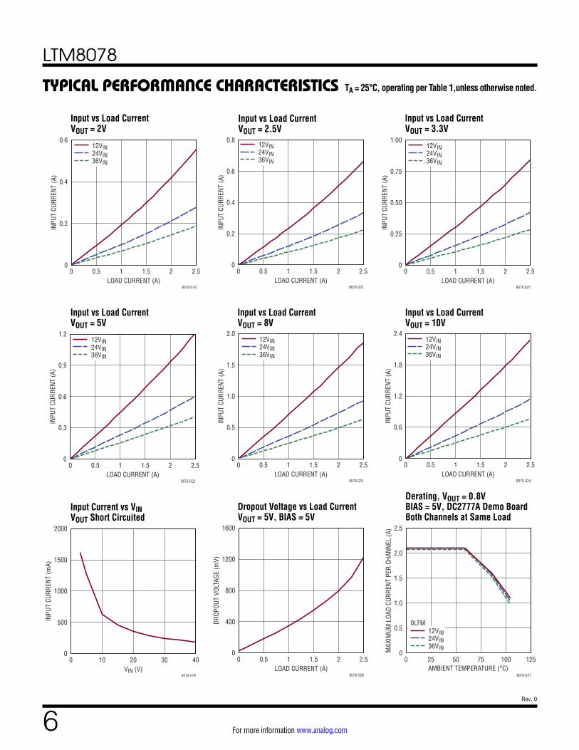
Input vs Load Current VOUT = 2V
Input vs Load Current VOUT = 2.5V
Input vs Load Current VOUT = 3.3V
Input vs Load Current VOUT = 5V
Input vs Load Current VOUT = 8V
Input vs Load Current VOUT = 10V
Input Current vs VIN VOUT Short Circuited
Dropout Voltage vs Load Current VOUT = 5V, BIAS = 5V
Derating, VOUT = 0.8V BIAS = 5V, DC2777A Demo Board Both Channels at Same Load
TA = 25°C, operating per Table 1,unless otherwise noted.TYPICAL PERFORMANCE CHARACTERISTICS
12VIN24VIN36VIN
LOAD CURRENT (A)0 0.5 1 1.5 2 2.5
0
0.2
0.4
0.6
INPU
T CU
RREN
T (A
)
VOUT = 2.0V
8078 G19
12VIN24VIN36VIN
LOAD CURRENT (A)0 0.5 1 1.5 2 2.5
0
0.2
0.4
0.6
0.8
INPU
T CU
RREN
T (A
)
8078 G20
12VIN24VIN36VIN
LOAD CURRENT (A)0 0.5 1 1.5 2 2.5
0
0.25
0.50
0.75
1.00
INPU
T CU
RREN
T (A
)
OUT
8078 G21
12VIN24VIN36VIN
LOAD CURRENT (A)0 0.5 1 1.5 2 2.5
0
0.3
0.6
0.9
1.2
INPU
T CU
RREN
T (A
)
OUT
8078 G22
12VIN24VIN36VIN
LOAD CURRENT (A)0 0.5 1 1.5 2 2.5
0
0.5
1.0
1.5
2.0
INPU
T CU
RREN
T (A
)
VOUT = 8V
8078 G23
12VIN24VIN36VIN
LOAD CURRENT (A)0 0.5 1 1.5 2 2.5
0
0.6
1.2
1.8
2.4
INPU
T CU
RREN
T (A
)
VOUT = 10V
8078 G24
VIN (V)0 10 20 30 40
0
500
1000
1500
2000
INPU
T CU
RREN
T (m
A)
VOUT Short Circuited
8078 G25
LOAD CURRENT (A)0 0.5 1 1.5 2 2.5
0
400
800
1200
1600
DROP
OUT
VOLT
AGE
(mV)
OUT
8078 G26
12VIN24VIN36VIN
0 25 50 75 100 1250
0.5
1.0
1.5
2.0
2.5
MAX
IMUM
LOA
D CU
RREN
T PE
R CH
ANNE
L (A
)
Both Channels At Same Load
8078 G27
AMBIENT TEMPERATURE (°C)
0LFM
LTM8078
7Rev. 0
For more information www.analog.com
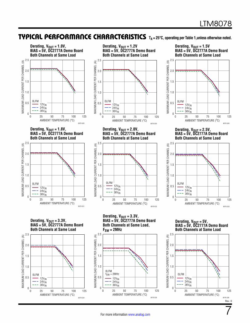
Derating, VOUT = 1.0V, BIAS = 5V, DC2777A Demo Board Both Channels at Same Load
Derating, VOUT = 1.2V BIAS = 5V, DC2777A Demo Board Both Channels at Same Load
Derating, VOUT = 1.5V BIAS = 5V, DC2777A Demo Board Both Channels at Same Load
Derating, VOUT = 2.5V, BIAS = 5V, DC2777A Demo Board Both Channels at Same Load
Derating, VOUT = 1.8V, BIAS = 5V, DC2777A Demo Board Both Channels at Same Load
Derating, VOUT = 2.0V, BIAS = 5V, DC2777A Demo Board Both Channels at Same Load
TA = 25°C, operating per Table 1,unless otherwise noted.TYPICAL PERFORMANCE CHARACTERISTICS
Derating, VOUT = 5V, BIAS = 5V, DC2777A Demo Board Both Channels at Same Load
Derating, VOUT = 3.3V, BIAS = 5V, DC2777A Demo Board Both Channels at Same Load
Derating, VOUT = 3.3V, BIAS = 5V, DC2777A Demo Board Both Channels at Same Load, FSW = 2MHz
12VIN24VIN36VIN
0 25 50 75 100 1250
0.5
1.0
1.5
2.0
2.5
MAX
IMUM
LOA
D CU
RREN
T PE
R CH
ANNE
L (A
)
Both Channels At Same Load
8078 G28
AMBIENT TEMPERATURE (°C)
0LFM12VIN24VIN36VIN
0 25 50 75 100 1250
0.5
1.0
1.5
2.0
2.5
MAX
IMUM
LOA
D CU
RREN
T PE
R CH
ANNE
L (A
)
Both Channels At Same Load
8078 G29
AMBIENT TEMPERATURE (°C)
0LFM12VIN24VIN36VIN
AMBIENT TEMPERATURE (oC)0 25 50 75 100 125
0
0.5
1.0
1.5
2.0
2.5
MAX
IMUM
LOA
D CU
RREN
T PE
R CH
ANNE
L (A
)
Both Channels At Same Load
8078 G30
0LFM
12VIN24VIN36VIN
0 25 50 75 100 1250
0.5
1.0
1.5
2.0
2.5
MAX
IMUM
LOA
D CU
RREN
T PE
R CH
ANNE
L (A
)
Both Channels At Same Load
8078 G31
AMBIENT TEMPERATURE (°C)
0LFM12VIN24VIN36VIN
AMBIENT TEMPERATURE (oC)0 25 50 75 100 125
0
0.5
1.0
1.5
2.0
2.5
MAX
IMUM
LOA
D CU
RREN
T PE
R CH
ANNE
L (A
)
8078 G32
0LFM12VIN24VIN36VIN
0 25 50 75 100 1250
0.5
1.0
1.5
2.0
2.5
MAX
IMUM
LOA
D CU
RREN
T PE
R CH
ANNE
L (A
)
Both Channels At Same Load
8078 G33
AMBIENT TEMPERATURE (°C)
0LFM
0LFM12VIN24VIN36VIN
0 25 50 75 100 1250
0.5
1.0
1.5
2.0
2.5
MAX
IMUM
LOA
D CU
RREN
T PE
R CH
ANNE
L (A
)
Both Channels At Same Load
8078 G34
AMBIENT TEMPERATURE (°C)
fSW = 2MHz
12VIN24VIN36VIN
0 25 50 75 100 1250
0.5
1.0
1.5
2.0
2.5
MAX
IMUM
LOA
D CU
RREN
T PE
R CH
ANNE
L (A
)
Both Channels At Same Load
8078 G35AMBIENT TEMPERATURE (°C)
0LFM0LFM
12VIN24VIN36VIN
0 25 50 75 100 1250
0.5
1.0
1.5
2.0
2.5
MAX
IMUM
LOA
D CU
RREN
T PE
R CH
ANNE
L (A
)
8078 G36AMBIENT TEMPERATURE (°C)
LTM8078
8Rev. 0
For more information www.analog.com
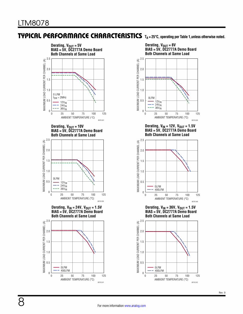
Derating, VOUT = 8V BIAS = 5V, DC2777A Demo Board Both Channels at Same Load
Derating, VOUT = 10V BIAS = 5V, DC2777A Demo Board Both Channels at Same Load
Derating, VIN = 12V, VOUT = 1.5V BIAS = 5V, DC2777A Demo Board Both Channels at Same Load
Derating, VIN = 24V, VOUT = 1.5V BIAS = 5V, DC2777A Demo Board Both Channels at Same Load
Derating, VIN = 36V, VOUT = 1.5V BIAS = 5V, DC2777A Demo Board Both Channels at Same Load
TA = 25°C, operating per Table 1,unless otherwise noted. TYPICAL PERFORMANCE CHARACTERISTICS
0LFM12VIN24VIN36VIN
0 25 50 75 100 1250
0.5
1.0
1.5
2.0
2.5
MAX
IMUM
LOA
D CU
RREN
T PE
R CH
ANNE
L (A
)
Both Channels At Same Load
8078 G39AMBIENT TEMPERATURE (°C)
0LFM400LFM
0 25 50 75 100 1250
0.5
1.0
1.5
2.0
2.5M
AXIM
UM L
OAD
CURR
ENT
PER
CHAN
NEL
(A)
Both Channels At Same Load
8078 G40AMBIENT TEMPERATURE (°C)
0LFM400LFM
0 25 50 75 100 1250
0.5
1.0
1.5
2.0
2.5
MAX
IMUM
LOA
D CU
RREN
T PE
R CH
ANNE
L (A
)
Both Channels At Same Load
8078 G41AMBIENT TEMPERATURE (°C)
0LFM400LFM
0 25 50 75 100 1250
0.5
1.0
1.5
2.0
2.5
MAX
IMUM
LOA
D CU
RREN
T PE
R CH
ANNE
L (A
)
Both Channels At Same Load
8078 G42AMBIENT TEMPERATURE (°C)
0LFM12VIN24VIN36VIN
0 25 50 75 100 1250
0.5
1.0
1.5
2.0
2.5
MAX
IMUM
LOA
D CU
RREN
T PE
R CH
ANNE
L (A
)
Both Channels At Same Load
8078 G38AMBIENT TEMPERATURE (°C)
Derating, VOUT = 5V BIAS = 5V, DC2777A Demo Board Both Channels at Same Load
fSW = 2MHz
12VIN24VIN36VIN
AMBIENT TEMPERATURE (°C)0 25 50 75 100 125
0
0.5
1.0
1.5
2.0
2.5
MAX
IMUM
LOA
D CU
RREN
T PE
R CH
ANNE
L (A
)
Both Channels At Same Load
8078 G37
0 LFM
LTM8078
9Rev. 0
For more information www.analog.com
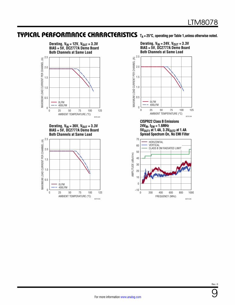
Derating, VIN = 12V, VOUT = 3.3V BIAS = 5V, DC2777A Demo Board Both Channels at Same Load
Derating, VIN = 24V, VOUT = 3.3V BIAS = 5V, DC2777A Demo Board Both Channels at Same Load
Derating, VIN = 36V, VOUT = 3.3V BIAS = 5V, DC2777A Demo Board Both Channels at Same Load
TA = 25°C, operating per Table 1,unless otherwise noted. TYPICAL PERFORMANCE CHARACTERISTICS
0LFM400LFM
0 25 50 75 100 1250
0.5
1.0
1.5
2.0
2.5
MAX
IMUM
LOA
D CU
RREN
T PE
R CH
ANNE
L (A
)
Both Channels At Same Load
8078 G43AMBIENT TEMPERATURE (°C)
0LFM400LFM
0 25 50 75 100 1250
0.5
1.0
1.5
2.0
2.5
MAX
IMUM
LOA
D CU
RREN
T PE
R CH
ANNE
L (A
)
Both Channels At Same Load
8078 G44AMBIENT TEMPERATURE (°C)
0LFM400LFM
AMBIENT TEMPERATURE (°C)0 25 50 75 100 125
0
0.5
1.0
1.5
2.0
2.5
MAX
IMUM
LOA
D CU
RREN
T PE
R CH
ANNE
L (A
)
Both Channels At Same Load
8078 G45
CISPR22 Class B Emissions 24VIN, fSW = 1.6MHz 5VOUT1 at 1.4A, 3.3VOUT2 at 1.4A Spread Spectrum On, No EMI Filter
HORIZONTALVERTICALCLASS B 3M RADIATED LIMIT
FREQUENCY (MHz)0 200 400 600 800 1000
–10
0
10
20
30
40
50
60
70
AMPL
ITUD
E (d
BuV/
m)
Spread Spectrum On, No EMI Filter
8078 G46
LTM8078
10Rev. 0
For more information www.analog.com
PIN FUNCTIONSVIN1 (Pin A3): Input Power for the Channel 1 Regulator. The VIN1 bank powers the internal control circuitry for both channels and is monitored by under voltage lockout circuitry. The VIN1 voltage must be greater than 3.0V for either channel of the LTM8078 to operate. Decouple VIN1 to ground with an external, low ESR capacitor. See Table 1 for recommended values.
VIN2 (Pin A4): Input Power for the Channel 2 Regulator. The VIN2 pin is monitored by under voltage lockout cir-cuitry. The VIN1 voltage must be greater than 3.0V and VIN2 must be greater than 2V for proper VIN2 operation. Decouple VIN2 to ground with an external, low ESR capaci-tor. See Table 1 for recommended values.
VOUT1/VOUT2 (Banks 1 and 2): Power Output for channels 1 and 2, Respectively. Apply the output filter capacitor and the output load between these pins and GND pins.
GND (Bank 3, Pin A7): Tie these GND pins to a local ground plane below the LTM8078 and the circuit compo-nents. In most applications, the bulk of the heat flow out of the LTM8078 is through these pads, so the printed circuit design has a large impact on the thermal performance of the part. See the PCB Layout and Thermal Considerations sections for more details. Return the feedback divider (RFB) to this net.
BIAS (Pin E7): The internal regulator will draw current from BIAS instead of VIN1 when BIAS is tied to a voltage higher than 3.2V. For output voltages of 3.3V and above this pin should be tied to VOUT. If this pin is tied to a sup-ply other than VOUT connect a local bypass capacitor to this pin.
CLKOUT (Pin D1): Synchronization Output. When SYNC > 2.8V, the CLKOUT pin provides a waveform about 90 degrees out-of-phase with Channel 1. This allows syn-chronization with other regulators with up to four phases. When an external clock is applied to the SYNC pin, the CLKOUT pin will output a waveform with about the same
phase, duty cycle, and frequency as the SYNC waveform. In Burst Mode operation, the CLKOUT pin will be internally grounded. Float this pin if the CLKOUT function is not used. Do not drive this pin.
FB1/FB2 (Pins D7, C7): The LTM8078 regulates the FBn pins to 800mV. Connect the feedback resistor to this pin to set the output voltage.
PG1/PG2 (Pins B1, A2): The PGn pins are the open-drain outputs of an internal comparator. PGn remains low until the FBn pin is within ±7.5% of the final regulation voltage, and there are no fault conditions. PGn is pulled low during VIN1 UVLO, VIN2 UVLO, thermal shutdown, or when the RUN pin is low.
RT (Pin B7): Connect a resistor between RT and ground to set the switching frequency of both channels. Do not drive this pin.
RUN (Pin A5): The LTM8078 is shut down when this pin is low and active when this pin is high. Tie to VINn if shutdown feature is not used. An external resistor divider from VINn can be used to program a VINn threshold below which the corresponding channel of the LTM8078 will shut down. Do not float this pin.
OM (Pin C6): Output Mode. Tie this pin to the adjacent OMC pin when the two LTM8078 outputs are regulating at different voltages. Float this pin when the two LTM8078 outputs are in parallel.
OMC (Pin D6): Output Mode Control. Float this pin when the two outputs of the LTM8078 are load sharing. Connect this pin to the OMC pin of other LTM8078s when mul-tiple LTM8078s are load sharing. When not load sharing, tie this pin to the adjacent OM pin. That is, when the VOUT1 and VOUT2 are independent voltages, connect OM to OMC. If VOUT1 and VOUT2 are independent and OM and OMC are not connected together, the LTM8078 will not regulate properly.
LTM8078
11Rev. 0
For more information www.analog.com
PIN FUNCTIONSTRSS1/TRSS2 (Pin B6, A6): Output Tracking and Soft-Start Pins. These pins allow user control of the output voltage ramp rate during startup. A TRSSn voltage below 0.8V forces the LTM8078 to regulate the FBn pin to equal the TRSSn pin voltage. When TRSSn is above 0.8V, the tracking function is disabled and the internal reference resumes control of the error amplifier. An internal 2μA pull-up current on this pin allows a capacitor to program output voltage slew rate. This pin is pulled to ground dur-ing shutdown and fault conditions; use a series resistor if driving from a low impedance output. This pin may be left floating if the soft-start feature is not being used.
SYNC (Pin C1): External Clock Synchronization Input. Ground this pin for low ripple Burst Mode operation at low output loads; this will also disable the CLKOUT func-tion. Apply a DC voltage between 2.8V and 4V for spread spectrum modulation. Float the SYNC pin for forced con-tinuous operation without spread spectrum modulation. Apply a clock source to the SYNC pin for synchronization to an external frequency. The LTM8078 will be in forced continuous mode when an external frequency is applied.
LTM8078
12Rev. 0
For more information www.analog.com
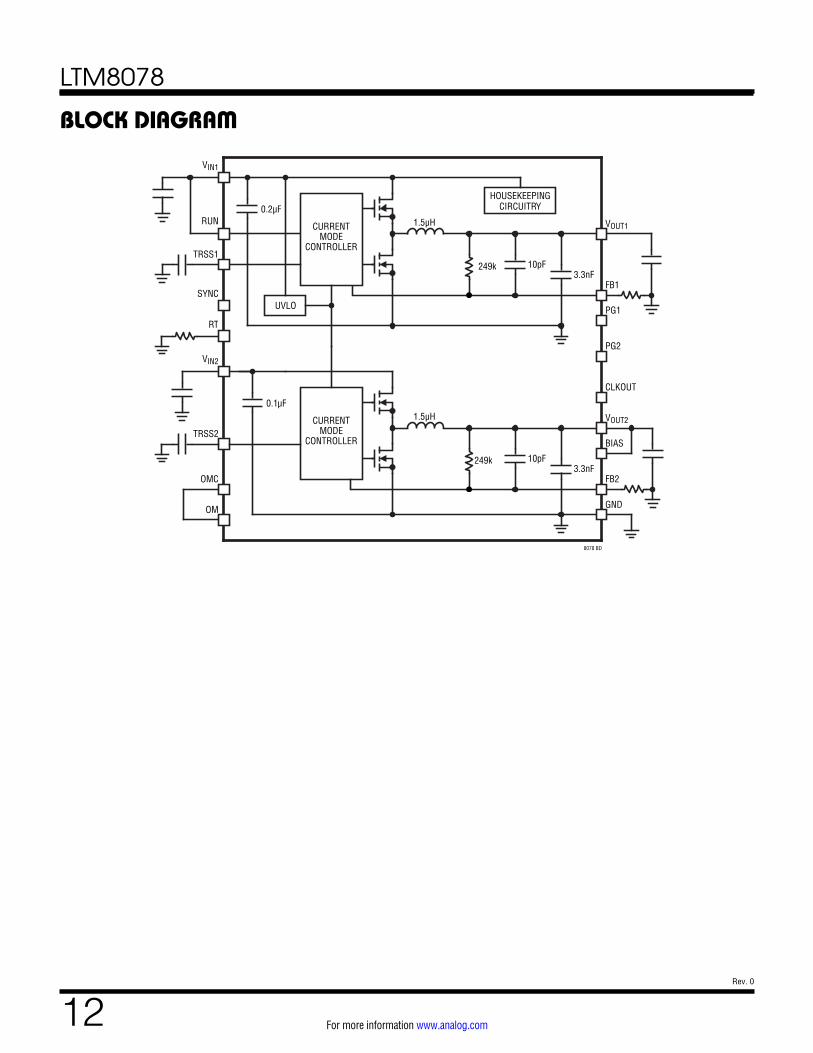
BLOCK DIAGRAM
10pF3.3nF
249k
1.5µH0.2µF
10pF3.3nF
249k
1.5µH0.1µF
CURRENTMODE
CONTROLLER
VIN1
RUN
TRSS1
SYNC
VOUT1
FB1
RTPG1
CLKOUT
CURRENTMODE
CONTROLLER
VIN2
TRSS2
VOUT2
FB2
GND
BIAS
OMC
OM
UVLO
HOUSEKEEPINGCIRCUITRY
PG2
8078 BD
LTM8078
13Rev. 0
For more information www.analog.com
OPERATIONThe LTM8078 is a dual standalone non-isolated step-down switching DC/DC power supply that can deliver a peak current of up to 2.5A per channel. The continuous current is determined by the internal operating tempera-ture. It provides a precisely regulated output voltage pro-grammable via one external resistor from 0.8V to 10V. The input voltage range for channel 1 is 3V to 40V, while the input voltage range for channel 2 is 2V to 40V. VIN1 must be 3V or above for either channel to operate.
Given that the LTM8078 is a step-down converter, make sure that the input voltage is high enough to support the desired output voltage and load current. See simplified Block Diagram.
The LTM8078 contains two current mode controllers, power switching elements, power inductors and a modest amount of input and output capacitance. The LTM8078 is a fixed frequency PWM regulator. The switching frequency is set by simply connecting the appropriate resistor value from the RT pin to GND.
An internal regulator provides power to the control cir-cuitry. This bias regulator normally draws power from the VIN1 pin, but if the BIAS pin is connected to an external voltage higher than 3.2V, bias power is drawn from the external source (typically the regulated output voltage). This improves efficiency. Tie BIAS to GND if it is not used.
To enhance efficiency, the LTM8078 automatically switches to Burst Mode operation in light or no load situations. Between bursts, all circuitry associated with controlling the output switch is shut down reducing the input supply current to just a few µA.
The TRSSn node acts as an auxiliary input to the error amplifier. The voltage at FB servos to the TRSS voltage until TRSS goes above 0.8V. Soft-start is implemented by generating a voltage ramp at the TRSS pin using an exter-nal capacitor which is charged by an internal constant current. Alternatively, driving the TRSS pin with a signal source or resistive network provides a tracking function. Do not drive the TRSS pin with a low impedance volt-age source. See the Applications Information section for more details.
The LTM8078 contains a power good comparator which trips when the FBn pin is at about 92% to 108% of its regulated value. The PGn output is an open-drain transis-tor that is off when the output is in regulation, allowing an external resistor to pull the PGn pin high. The PG1 signal is valid when VIN1 is above 3V. Similarly, the PG2 signal is valid when VIN2 is above 2V.
The LTM8078 is equipped with a thermal shutdown that inhibits power switching at high junction temperatures. The activation threshold of this function is above the max-imum temperature rating to avoid interfering with normal operation, so prolonged or repetitive operation under a condition in which the thermal shutdown activates may damage or impair the reliability of the device.
LTM8078
14Rev. 0
For more information www.analog.com
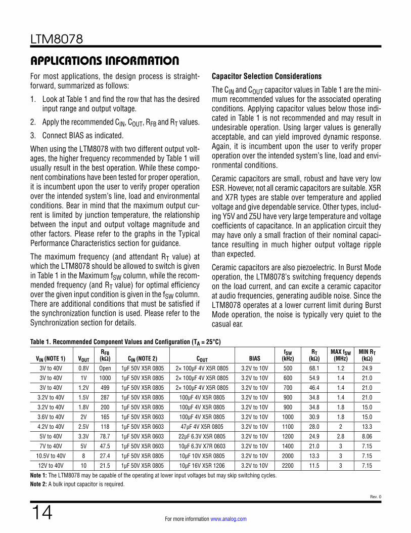
For most applications, the design process is straight-forward, summarized as follows:
1. Look at Table 1 and find the row that has the desired input range and output voltage.
2. Apply the recommended CIN, COUT, RFB and RT values.
3. Connect BIAS as indicated.
When using the LTM8078 with two different output volt-ages, the higher frequency recommended by Table 1 will usually result in the best operation. While these compo-nent combinations have been tested for proper operation, it is incumbent upon the user to verify proper operation over the intended system’s line, load and environmental conditions. Bear in mind that the maximum output cur-rent is limited by junction temperature, the relationship between the input and output voltage magnitude and other factors. Please refer to the graphs in the Typical Performance Characteristics section for guidance.
The maximum frequency (and attendant RT value) at which the LTM8078 should be allowed to switch is given in Table 1 in the Maximum fSW column, while the recom-mended frequency (and RT value) for optimal efficiency over the given input condition is given in the fSW column. There are additional conditions that must be satisfied if the synchronization function is used. Please refer to the Synchronization section for details.
APPLICATIONS INFORMATIONCapacitor Selection Considerations
The CIN and COUT capacitor values in Table 1 are the mini-mum recommended values for the associated operating conditions. Applying capacitor values below those indi-cated in Table 1 is not recommended and may result in undesirable operation. Using larger values is generally acceptable, and can yield improved dynamic response. Again, it is incumbent upon the user to verify proper operation over the intended system’s line, load and envi-ronmental conditions.
Ceramic capacitors are small, robust and have very low ESR. However, not all ceramic capacitors are suitable. X5R and X7R types are stable over temperature and applied voltage and give dependable service. Other types, includ-ing Y5V and Z5U have very large temperature and voltage coefficients of capacitance. In an application circuit they may have only a small fraction of their nominal capaci-tance resulting in much higher output voltage ripple than expected.
Ceramic capacitors are also piezoelectric. In Burst Mode operation, the LTM8078’s switching frequency depends on the load current, and can excite a ceramic capacitor at audio frequencies, generating audible noise. Since the LTM8078 operates at a lower current limit during Burst Mode operation, the noise is typically very quiet to the casual ear.
Table 1. Recommended Component Values and Configuration (TA = 25°C)
VIN (NOTE 1) VOUT
RFB (kΩ) CIN (NOTE 2) COUT BIAS
fSW (kHz)
RT (kΩ)
MAX fSW (MHz)
MIN RT (kΩ)
3V to 40V 0.8V Open 1µF 50V X5R 0805 2× 100µF 4V X5R 0805 3.2V to 10V 500 68.1 1.2 24.9
3V to 40V 1V 1000 1µF 50V X5R 0805 2× 100µF 4V X5R 0805 3.2V to 10V 600 54.9 1.4 21.0
3V to 40V 1.2V 499 1µF 50V X5R 0805 2× 100µF 4V X5R 0805 3.2V to 10V 700 46.4 1.4 21.0
3.2V to 40V 1.5V 287 1µF 50V X5R 0805 100µF 4V X5R 0805 3.2V to 10V 900 34.8 1.4 21.0
3.2V to 40V 1.8V 200 1µF 50V X5R 0805 100µF 4V X5R 0805 3.2V to 10V 900 34.8 1.8 15.0
3.6V to 40V 2V 165 1µF 50V X5R 0603 100µF 4V X5R 0805 3.2V to 10V 1000 30.9 1.8 15.0
4.2V to 40V 2.5V 118 1µF 50V X5R 0603 47µF 4V X5R 0805 3.2V to 10V 1100 28.0 2 13.3
5V to 40V 3.3V 78.7 1µF 50V X5R 0603 22µF 6.3V X5R 0805 3.2V to 10V 1200 24.9 2.8 8.06
7V to 40V 5V 47.5 1µF 50V X5R 0603 10µF 6.3V X7R 0603 3.2V to 10V 1400 21.0 3 7.15
10.5V to 40V 8 27.4 1µF 50V X5R 0805 10µF 10V X5R 0805 3.2V to 10V 2000 13.3 3 7.15
12V to 40V 10 21.5 1µF 50V X5R 0805 10µF 16V X5R 1206 3.2V to 10V 2200 11.5 3 7.15
Note 1: The LTM8078 may be capable of the operating at lower input voltages but may skip switching cycles.Note 2: A bulk input capacitor is required.
LTM8078
15Rev. 0
For more information www.analog.com
APPLICATIONS INFORMATIONIf this audible noise is unacceptable, use a high perfor-mance electrolytic capacitor at the output. It may also be a parallel combination of a ceramic capacitor and a low cost electrolytic capacitor.
A final precaution regarding ceramic capacitors concerns the maximum input voltage rating of the LTM8078. A ceramic input capacitor combined with trace or cable inductance forms a high-Q (underdamped) tank circuit. If the LTM8078 circuit is plugged into a live supply, the input voltage can ring to twice its nominal value, possi-bly exceeding the device’s rating. This situation is easily avoided; see the Hot-Plugging Safely section.
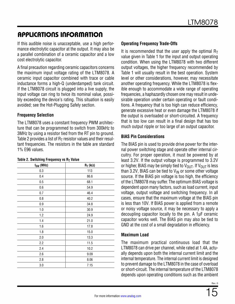
Frequency Selection
The LTM8078 uses a constant frequency PWM architec-ture that can be programmed to switch from 300kHz to 3MHz by using a resistor tied from the RT pin to ground. Table 2 provides a list of RT resistor values and their resul-tant frequencies. The resistors in the table are standard 1% E96 values.
Operating Frequency Trade-Offs
It is recommended that the user apply the optimal RT value given in Table 1 for the input and output operating condition. When using the LTM8078 with two different output voltages, the higher frequency recommended by Table 1 will usually result in the best operation. System level or other considerations, however, may necessitate another operating frequency. While the LTM8078 is flex-ible enough to accommodate a wide range of operating frequencies, a haphazardly chosen one may result in unde-sirable operation under certain operating or fault condi-tions. A frequency that is too high can reduce efficiency, generate excessive heat or even damage the LTM8078 if the output is overloaded or short-circuited. A frequency that is too low can result in a final design that has too much output ripple or too large of an output capacitor.
BIAS Pin Considerations
The BIAS pin is used to provide drive power for the inter-nal power switching stage and operate other internal cir-cuitry. For proper operation, it must be powered by at least 3.2V. If the output voltage is programmed to 3.2V or higher, BIAS may be simply tied to VOUT. If VOUT is less than 3.2V, BIAS can be tied to VIN or some other voltage source. If the BIAS pin voltage is too high, the efficiency of the LTM8078 may suffer. The optimum BIAS voltage is dependent upon many factors, such as load current, input voltage, output voltage and switching frequency. In all cases, ensure that the maximum voltage at the BIAS pin is less than 10V. If BIAS power is applied from a remote or noisy voltage source, it may be necessary to apply a decoupling capacitor locally to the pin. A 1µF ceramic capacitor works well. The BIAS pin may also be tied to GND at the cost of a small degradation in efficiency.
Maximum Load
The maximum practical continuous load that the LTM8078 can drive per channel, while rated at 1.4A, actu-ally depends upon both the internal current limit and the internal temperature. The internal current limit is designed to prevent damage to the LTM8078 in the case of overload or short-circuit. The internal temperature of the LTM8078 depends upon operating conditions such as the ambient
Table 2. Switching Frequency vs RT ValuefSW (MHz) RT (kΩ)
0.3 113
0.4 86.6
0.5 68.1
0.6 54.9
0.7 46.4
0.8 40.2
0.9 34.8
1.0 30.9
1.2 24.9
1.4 21.0
1.6 17.8
1.8 15.0
2.0 13.3
2.2 11.5
2.4 10.2
2.6 9.09
2.8 8.06
3.0 7.15
Table 1. Recommended Component Values and Configuration (TA = 25°C)
VIN (NOTE 1) VOUT
RFB (kΩ) CIN (NOTE 2) COUT BIAS
fSW (kHz)
RT (kΩ)
MAX fSW (MHz)
MIN RT (kΩ)
3V to 40V 0.8V Open 1µF 50V X5R 0805 2× 100µF 4V X5R 0805 3.2V to 10V 500 68.1 1.2 24.9
3V to 40V 1V 1000 1µF 50V X5R 0805 2× 100µF 4V X5R 0805 3.2V to 10V 600 54.9 1.4 21.0
3V to 40V 1.2V 499 1µF 50V X5R 0805 2× 100µF 4V X5R 0805 3.2V to 10V 700 46.4 1.4 21.0
3.2V to 40V 1.5V 287 1µF 50V X5R 0805 100µF 4V X5R 0805 3.2V to 10V 900 34.8 1.4 21.0
3.2V to 40V 1.8V 200 1µF 50V X5R 0805 100µF 4V X5R 0805 3.2V to 10V 900 34.8 1.8 15.0
3.6V to 40V 2V 165 1µF 50V X5R 0603 100µF 4V X5R 0805 3.2V to 10V 1000 30.9 1.8 15.0
4.2V to 40V 2.5V 118 1µF 50V X5R 0603 47µF 4V X5R 0805 3.2V to 10V 1100 28.0 2 13.3
5V to 40V 3.3V 78.7 1µF 50V X5R 0603 22µF 6.3V X5R 0805 3.2V to 10V 1200 24.9 2.8 8.06
7V to 40V 5V 47.5 1µF 50V X5R 0603 10µF 6.3V X7R 0603 3.2V to 10V 1400 21.0 3 7.15
10.5V to 40V 8 27.4 1µF 50V X5R 0805 10µF 10V X5R 0805 3.2V to 10V 2000 13.3 3 7.15
12V to 40V 10 21.5 1µF 50V X5R 0805 10µF 16V X5R 1206 3.2V to 10V 2200 11.5 3 7.15
Note 1: The LTM8078 may be capable of the operating at lower input voltages but may skip switching cycles.Note 2: A bulk input capacitor is required.
LTM8078
16Rev. 0
For more information www.analog.com
APPLICATIONS INFORMATIONtemperature, the power delivered, and the heat sinking capability of the system. For example, if a single LTM8078 is configured to regulate at 1V, and channel 2 is turned off, channel 1 may continuously deliver 2.5A from 12VIN if the ambient temperature is controlled to less than 60°C. This is quite a bit higher than the 1.4A continu-ous rating. Please see graphs in the Typical Performance Characteristics section. Similarly, if both channels of the LTM8078 are delivering 8VOUT and the ambient tempera-ture is 100°C, each channel will deliver at most 0.6A from 24VIN, which is less than the 1.4A continuous rating.
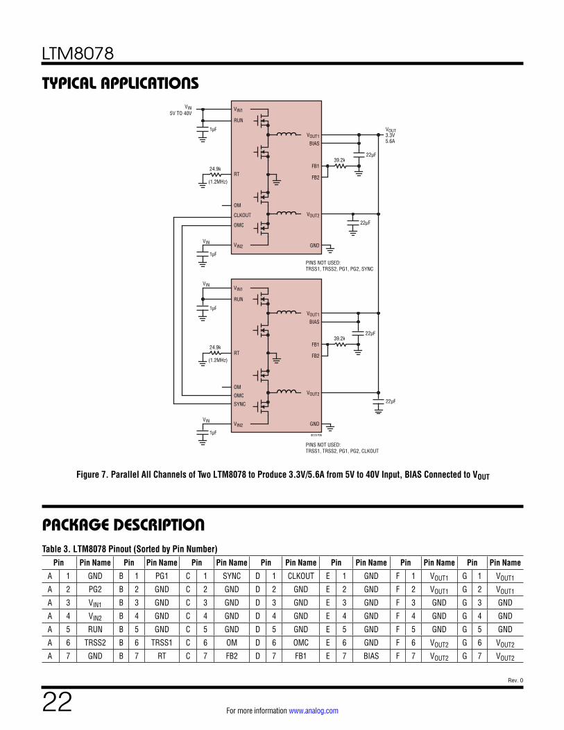
Load Sharing
The two LTM8078 channels may be paralleled to produce higher currents. To do this on two or more LTM8078, tie the VIN, VOUT, FB and OMC pins of all the paralleled channels/modules together (see Figure 7). If only the two channels of a LTM8078 are paralleled, leave OMC and OM floating. To ensure that paralleled channels start up together, the TRSS pins may be tied together, as well. If it is inconvenient to tie the TRSS pins together, make sure that the same value soft-start capacitors are used for each µModule regulator. When load sharing among n units and using a single RFB resistor, the value of the resistor is:
RFB =
199.2n(VOUT − 0.8)
,where RFB is in kΩ
When the LTM8078 outputs regulate independently, tie OM to OMC. Examples of load sharing applications are given in Figure 4 through Figure 6.
Burst Mode Operation
To enhance efficiency at light loads, the LTM8078 automatically switches to Burst Mode operation which keeps the output capacitor charged to the proper volt-age while minimizing the input quiescent current. During Burst Mode operation, the LTM8078 delivers single cycle bursts of current to the output capacitor followed by sleep periods where most of the internal circuitry is powered off and energy is delivered to the load by the output capacitor. During the sleep time, VIN and BIAS quiescent currents
are greatly reduced, so, as the load current decreases towards a no load condition, the percentage of time that the LTM8078 operates in sleep mode increases and the average input current is greatly reduced, resulting in higher light load efficiency.
Burst Mode operation is enabled by tying SYNC to GND.
Minimum Input Voltage
The LTM8078 is a step-down converter, so a minimum amount of headroom is required to keep the output in regulation. Keep the input above 3V to ensure proper operation. Voltage transients or ripple valleys that cause the input to fall below 3V may turn off the LTM8078.
VIN1 must be above 3V for either channel to operate. If VIN1 is above 3V, channel 2 will operate as long as VIN2 is above 2V.
Output Voltage Tracking and Soft-Start
The LTM8078 allows the user to adjust its output volt-age ramp rate by means of the TRSS pin. An internal 2μA pulls up the TRSSn pin to about 2.4V. Putting an external capacitor on TRSSn enables soft starting the out-put to reduce current surges on the input supply. During the soft-start ramp the output voltage will proportionally track the TRSSn pin voltage. For output tracking applica-tions, TRSSn can be externally driven by another voltage source. From 0V to 0.8V, the TRSSn voltage will override the internal 0.8V reference input to the error amplifier, thus regulating the FBn pin voltage to that of the TRSSn pin. When TRSSn is above 0.8V, tracking is disabled and the feedback voltage will regulate to the internal reference voltage. The TRSSn pin may be left floating if the function is not needed.
An active pull-down circuit is connected to the TRSSn pin which will discharge the external soft-start capacitor in the case of fault conditions and restart the ramp when the faults are cleared. Fault conditions that clear the soft-start capacitor are the RUNn pin transitioning low, VINn voltage falling too low, or thermal shutdown.
LTM8078
17Rev. 0
For more information www.analog.com
APPLICATIONS INFORMATIONPre-Biased Output
As discussed in the Output Voltage Tracking and Soft-Start section, the LTM8078 regulates the output to the FB voltage determined by the TRSSn pin whenever TRSSn is less than 0.8V. If the LTM8078 output is higher than the target output voltage, and SYNC is not held below 0.8V, the LTM8078 will attempt to regulate the output to the target voltage by returning a small amount of energy back to the input supply. If there is nothing loading the input supply, its voltage may rise. Take care that it does not rise so high that the input voltage exceeds the absolute maximum rating of the LTM8078. If SYNC is grounded, the LTM8078 will not return current to the input.
Synchronization
To select low ripple Burst Mode operation, tie the SYNC pin below about 0.8V (this can be ground or a logic low output). To synchronize the LTM8078 oscillator to an external frequency, connect a square wave (with about 20% to 80% duty cycle) to the SYNC pin. The square wave amplitude should have valleys that are below 0.8V and peaks above 1.5V.
The LTM8078 may be synchronized over a 300kHz to 3MHz range. The LTM8078 will not enter Burst Mode operation at light output loads while synchronized to an external clock. The RT resistor should be chosen to set the switching frequency equal to or below the lowest synchronization input. For example, if the synchroniza-tion signal will be 500kHz and higher, the RT should be selected for 500kHz or lower.
The LTM8078 features spread spectrum operation to fur-ther reduce EMI/EMC emissions. To enable spread spec-trum operation, apply between 2.8V and 4V to the SYNC pin. In this mode, triangular frequency modulation is used to vary the switching frequency between the value pro-grammed by RT to about 20% higher than that value. The
modulation frequency is about 5kHz. For example, when the LTM8078 is programmed to 2MHz, the frequency will vary from 2MHz to 2.4MHz at a 5kHz rate. When spread spectrum operation is selected, Burst Mode operation is disabled, and the part may run in discontinuous mode.
Shorted Input Protection
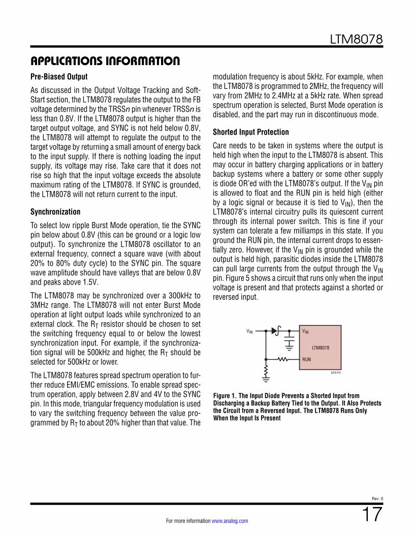
Care needs to be taken in systems where the output is held high when the input to the LTM8078 is absent. This may occur in battery charging applications or in battery backup systems where a battery or some other supply is diode OR’ed with the LTM8078’s output. If the VIN pin is allowed to float and the RUN pin is held high (either by a logic signal or because it is tied to VIN), then the LTM8078’s internal circuitry pulls its quiescent current through its internal power switch. This is fine if your system can tolerate a few milliamps in this state. If you ground the RUN pin, the internal current drops to essen-tially zero. However, if the VIN pin is grounded while the output is held high, parasitic diodes inside the LTM8078 can pull large currents from the output through the VIN pin. Figure 5 shows a circuit that runs only when the input voltage is present and that protects against a shorted or reversed input.
Figure 1. The Input Diode Prevents a Shorted Input from Discharging a Backup Battery Tied to the Output. It Also Protects the Circuit from a Reversed Input. The LTM8078 Runs Only When the Input Is Present
VIN
RUN
VIN
LTM8078
8078 F01
LTM8078
18Rev. 0
For more information www.analog.com
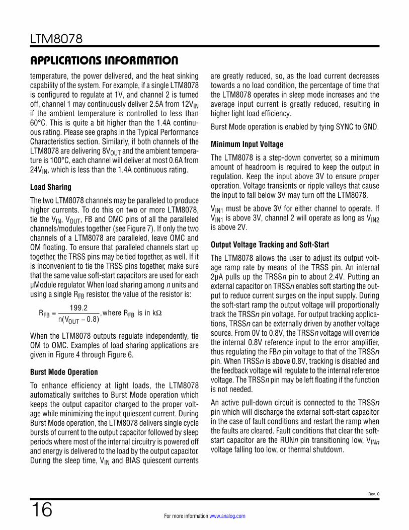
APPLICATIONS INFORMATIONPCB Layout
Most of the headaches associated with PCB layout have been alleviated or even eliminated by the high level of integration of the LTM8078. The LTM8078 is neverthe-less a switching power supply, and care must be taken to minimize EMI and ensure proper operation. Even with the high level of integration, you may fail to achieve specified operation with a haphazard or poor layout. See Figure 2 for a suggested layout. Ensure that the grounding and heat sinking are acceptable.
A few rules to keep in mind are:
1. Place the RFB and RT resistors as close as possible to their respective pins.
2. Place the CIN capacitor as close as possible to the VIN and GND connection of the LTM8078.
3. Place the COUT capacitor as close as possible to the VOUT and GND connection of the LTM8078.
4. Place the CIN and COUT capacitors such that their ground current flow directly adjacent to or underneath the LTM8078.
5. Connect all of the GND connections to as large a cop-per pour or plane area as possible on the top layer. Avoid breaking the ground connection between the external components and the LTM8078.
6. Use vias to connect the GND copper area to the board’s internal ground planes. Liberally distribute these GND vias to provide both a good ground con-nection and thermal path to the internal planes of the printed circuit board. Pay attention to the location and density of the thermal vias in Figure 2. The LTM8078 can benefit from the heat sinking afforded by vias that connect to internal GND planes at these locations, due to their proximity to internal power handling components. The optimum number of thermal vias depends upon the printed circuit board design. For example, a board might use very small via holes. It should employ more thermal vias than a board that uses larger holes.
Hot-Plugging Safely
The small size, robustness and low impedance of ceramic capacitors make them an attractive option for the input bypass capacitor of LTM8078. However, these capacitors can cause problems if the LTM8078 is plugged into a live supply (see Application Note 88 for a complete dis-cussion). The low loss ceramic capacitor combined with stray inductance in series with the power source forms an underdamped tank circuit, and the voltage at the VIN pin of the LTM8078 can ring to more than twice the nominal input voltage, possibly exceeding the LTM8078’s rating and damaging the part. If the input supply is poorly con-trolled or the LTM8078 is hot-plugged into an energized supply, the input network should be designed to prevent this overshoot. This can be accomplished by installing a small resistor in series to VIN, but the most popular method of controlling input voltage overshoot is add an electrolytic bulk cap to the VIN net. This capacitor’s rela-tively high equivalent series resistance damps the circuit and eliminates the voltage overshoot. The extra capacitor improves low frequency ripple filtering and can slightly improve the efficiency of the circuit, though it is likely to be the largest component in the circuit.
Figure 2. Layout Showing Suggested External Components, GND Plane and Thermal Vias
RT BIASFB1FB2
GND PLANE
TRSS2 TRSS1 OM OMC VOUT2
VIN2
VIN1
PG2
PG1 SYNC CLKOUT
RUN
VOUT2
GND PLANE
GND/THERMAL VIA
COUT1
CIN1
COUT2
CIN2
8078 F02
LTM8078
19Rev. 0
For more information www.analog.com
APPLICATIONS INFORMATIONThermal Considerations
The LTM8078 output current may need to be derated if it is required to operate in a high ambient temperature. The amount of current derating is dependent upon the input voltage, output power and ambient temperature. The derating curves given in the Typical Performance Characteristics section can be used as a guide. These curves were generated by the LTM8078 mounted to a 58cm2 4-layer FR4 printed circuit board. Boards of other sizes and layer count can exhibit different thermal behavior, so it is incumbent upon the user to verify proper operation over the intended system’s line, load and envi-ronmental operating conditions.
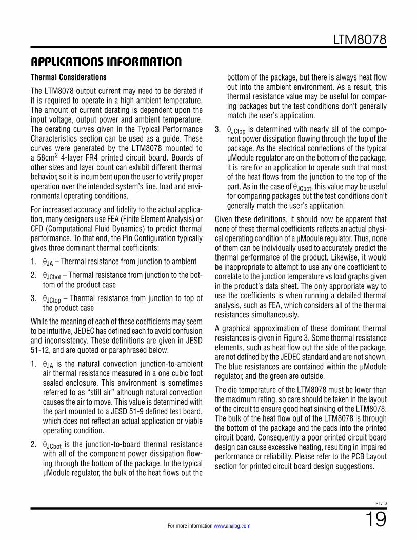
For increased accuracy and fidelity to the actual applica-tion, many designers use FEA (Finite Element Analysis) or CFD (Computational Fluid Dynamics) to predict thermal performance. To that end, the Pin Configuration typically gives three dominant thermal coefficients:
1. θJA – Thermal resistance from junction to ambient
2. θJCbot – Thermal resistance from junction to the bot-tom of the product case
3. θJCtop – Thermal resistance from junction to top of the product case
While the meaning of each of these coefficients may seem to be intuitive, JEDEC has defined each to avoid confusion and inconsistency. These definitions are given in JESD 51-12, and are quoted or paraphrased below:
1. θJA is the natural convection junction-to-ambient air thermal resistance measured in a one cubic foot sealed enclosure. This environment is sometimes referred to as “still air” although natural convection causes the air to move. This value is determined with the part mounted to a JESD 51-9 defined test board, which does not reflect an actual application or viable operating condition.
2. θJCbot is the junction-to-board thermal resistance with all of the component power dissipation flow-ing through the bottom of the package. In the typical µModule regulator, the bulk of the heat flows out the
bottom of the package, but there is always heat flow out into the ambient environment. As a result, this thermal resistance value may be useful for compar-ing packages but the test conditions don’t generally match the user’s application.
3. θJCtop is determined with nearly all of the compo-nent power dissipation flowing through the top of the package. As the electrical connections of the typical µModule regulator are on the bottom of the package, it is rare for an application to operate such that most of the heat flows from the junction to the top of the part. As in the case of θJCbot, this value may be useful for comparing packages but the test conditions don’t generally match the user’s application.
Given these definitions, it should now be apparent that none of these thermal coefficients reflects an actual physi-cal operating condition of a µModule regulator. Thus, none of them can be individually used to accurately predict the thermal performance of the product. Likewise, it would be inappropriate to attempt to use any one coefficient to correlate to the junction temperature vs load graphs given in the product’s data sheet. The only appropriate way to use the coefficients is when running a detailed thermal analysis, such as FEA, which considers all of the thermal resistances simultaneously.
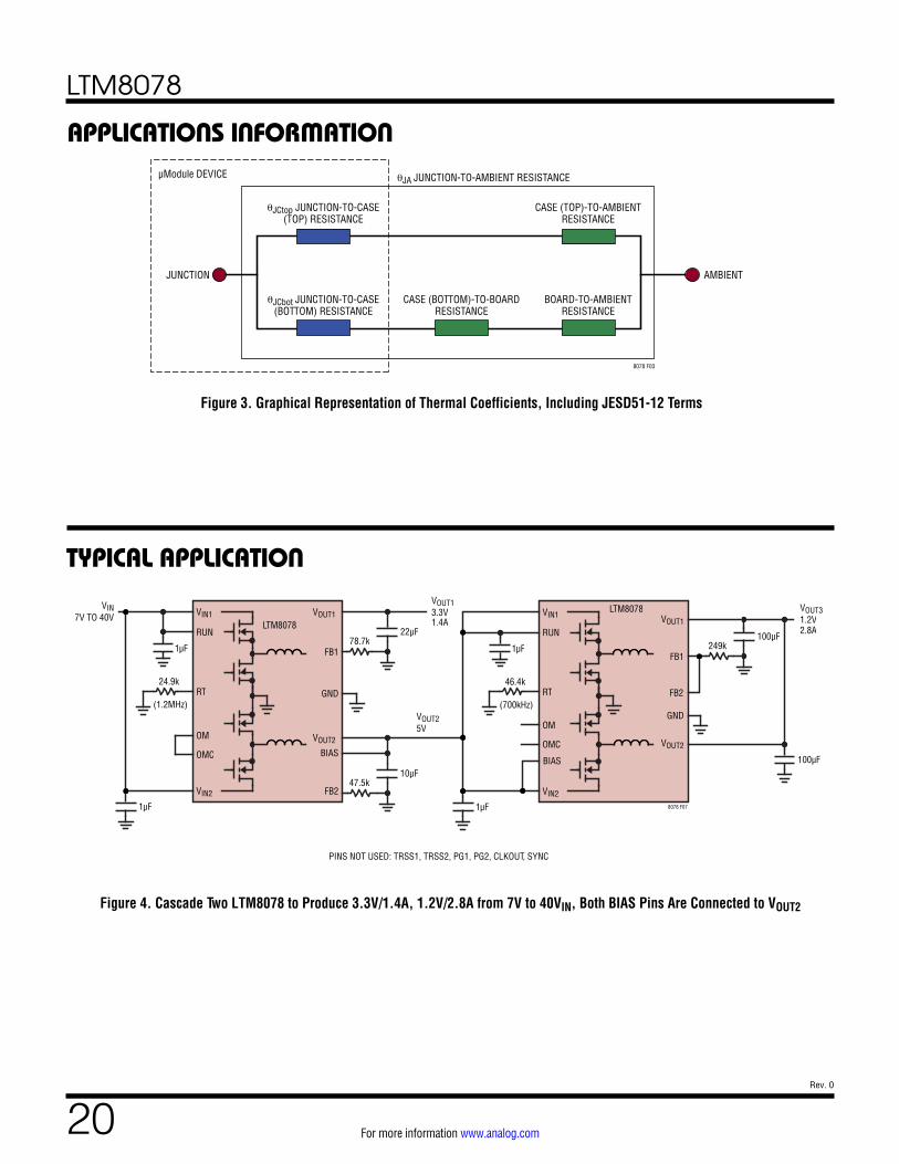
A graphical approximation of these dominant thermal resistances is given in Figure 3. Some thermal resistance elements, such as heat flow out the side of the package, are not defined by the JEDEC standard and are not shown. The blue resistances are contained within the µModule regulator, and the green are outside.
The die temperature of the LTM8078 must be lower than the maximum rating, so care should be taken in the layout of the circuit to ensure good heat sinking of the LTM8078. The bulk of the heat flow out of the LTM8078 is through the bottom of the package and the pads into the printed circuit board. Consequently a poor printed circuit board design can cause excessive heating, resulting in impaired performance or reliability. Please refer to the PCB Layout section for printed circuit board design suggestions.
LTM8078
20Rev. 0
For more information www.analog.com
Figure 3. Graphical Representation of Thermal Coefficients, Including JESD51-12 Terms
APPLICATIONS INFORMATION
8078 F03
µModule DEVICE
θJCtop JUNCTION-TO-CASE(TOP) RESISTANCE
θJA JUNCTION-TO-AMBIENT RESISTANCE
CASE (TOP)-TO-AMBIENTRESISTANCE
BOARD-TO-AMBIENTRESISTANCE
θJCbot JUNCTION-TO-CASE(BOTTOM) RESISTANCE
JUNCTION AMBIENT
CASE (BOTTOM)-TO-BOARDRESISTANCE
TYPICAL APPLICATION
Figure 4. Cascade Two LTM8078 to Produce 3.3V/1.4A, 1.2V/2.8A from 7V to 40VIN, Both BIAS Pins Are Connected to VOUT2
1µF
24.9k
47.5k10µF
78.7k22µF
1µF
VIN1
RUN
VOUT1
FB1
RT
VIN2
VOUT2
FB2
GND
BIAS
(1.2MHz)VOUT25V
VOUT13.3V1.4A
VIN7V TO 40V
PINS NOT USED: TRSS1, TRSS2, PG1, PG2, CLKOUT, SYNC
OM
OMC
VOUT1
VOUT2
BIAS
1µF
46.4k
1µF
VIN1
RUN
RT
VIN2
(700kHz)
OM
OMC
8078 F07
100µF
249k100µF
FB1
FB2
GND
VOUT31.2V2.8ALTM8078
LTM8078
LTM8078
21Rev. 0
For more information www.analog.com
TYPICAL APPLICATIONS
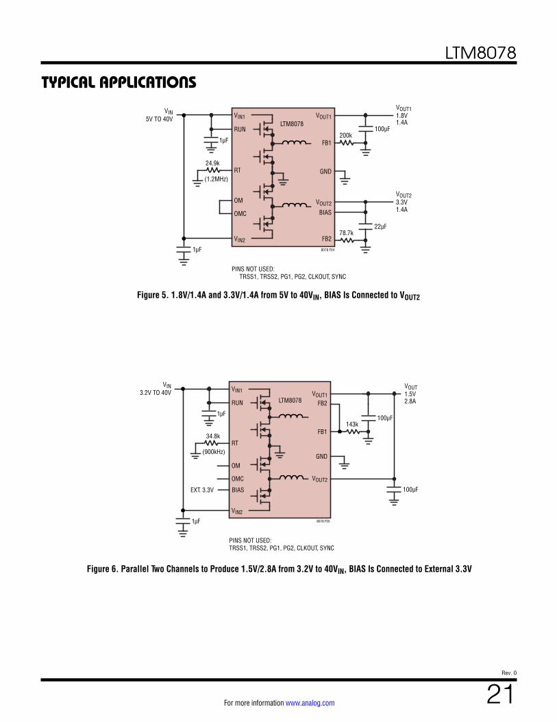
Figure 5. 1.8V/1.4A and 3.3V/1.4A from 5V to 40VIN, BIAS Is Connected to VOUT2
Figure 6. Parallel Two Channels to Produce 1.5V/2.8A from 3.2V to 40VIN, BIAS Is Connected to External 3.3V
1µF
24.9k
78.7k22µF
200k100µF
1µF
VIN1
RUN
VOUT1
FB1
RT
VIN2
VOUT2
FB2
GND
BIAS
(1.2MHz)
VOUT23.3V1.4A
VOUT11.8V1.4A
VIN5V TO 40V
PINS NOT USED: TRSS1, TRSS2, PG1, PG2, CLKOUT, SYNC
OM
OMC
8078 F04
LTM8078
VOUT1
VOUT2
BIASEXT. 3.3V
1µF
34.8k
1µF
VIN1
RUN
RT
VIN2
(900kHz)
VIN3.2V TO 40V
PINS NOT USED:TRSS1, TRSS2, PG1, PG2, CLKOUT, SYNC
OM
OMC
8078 F05
100µF
143k100µF
FB1
FB2
GND
VOUT1.5V2.8ALTM8078
LTM8078
22Rev. 0
For more information www.analog.com
PACKAGE DESCRIPTIONTable 3. LTM8078 Pinout (Sorted by Pin Number)
Pin Pin Name Pin Pin Name Pin Pin Name Pin Pin Name Pin Pin Name Pin Pin Name Pin Pin Name
A 1 GND B 1 PG1 C 1 SYNC D 1 CLKOUT E 1 GND F 1 VOUT1 G 1 VOUT1
A 2 PG2 B 2 GND C 2 GND D 2 GND E 2 GND F 2 VOUT1 G 2 VOUT1
A 3 VIN1 B 3 GND C 3 GND D 3 GND E 3 GND F 3 GND G 3 GND
A 4 VIN2 B 4 GND C 4 GND D 4 GND E 4 GND F 4 GND G 4 GND
A 5 RUN B 5 GND C 5 GND D 5 GND E 5 GND F 5 GND G 5 GND
A 6 TRSS2 B 6 TRSS1 C 6 OM D 6 OMC E 6 GND F 6 VOUT2 G 6 VOUT2
A 7 GND B 7 RT C 7 FB2 D 7 FB1 E 7 BIAS F 7 VOUT2 G 7 VOUT2
Figure 7. Parallel All Channels of Two LTM8078 to Produce 3.3V/5.6A from 5V to 40V Input, BIAS Connected to VOUT
1µF
24.9k
22µF
39.2k22µF
1µF
1µF
24.9k
22µF
39.2k22µF
1µF
VIN1
RUN
VOUT1
FB1
RT
VIN2
VOUT2
FB2
GND
BIAS
(1.2MHz)
PINS NOT USED: TRSS1, TRSS2, PG1, PG2, CLKOUT
OM
OMC
VIN1
RUN
VOUT1
FB1
RT
VIN2
VOUT2
FB2
GND
BIAS
(1.2MHz)
VOUT3.3V5.6A
VIN5V TO 40V
PINS NOT USED:TRSS1, TRSS2, PG1, PG2, SYNC
OM
OMC
VIN
VIN
VIN
CLKOUT
SYNC
8078 F06
TYPICAL APPLICATIONS
LTM8078
23Rev. 0
For more information www.analog.com
Information furnished by Analog Devices is believed to be accurate and reliable. However, no responsibility is assumed by Analog Devices for its use, nor for any infringements of patents or other rights of third parties that may result from its use. Specifications subject to change without notice. No license is granted by implication or otherwise under any patent or patent rights of Analog Devices.
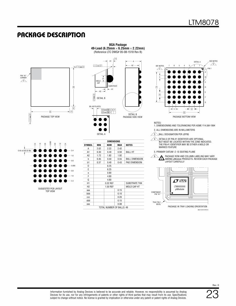
PACKAGE DESCRIPTION
PACKAGE TOP VIEW
4
PIN “A1”CORNER
DETAIL A
PACKAGE BOTTOM VIEW
3
SEE NOTES
G
F
E
D
C
B
A
1234567
PIN 1
NOTES:1. DIMENSIONING AND TOLERANCING PER ASME Y14.5M-1994
2. ALL DIMENSIONS ARE IN MILLIMETERS
BALL DESIGNATION PER JEP95
4
3
DETAILS OF PIN #1 IDENTIFIER ARE OPTIONAL,BUT MUST BE LOCATED WITHIN THE ZONE INDICATED.THE PIN #1 IDENTIFIER MAY BE EITHER A MOLD OR MARKED FEATURE
A
DETAIL BPACKAGE SIDE VIEW
A2
e
b
eb
F
G
SUGGESTED PCB LAYOUTTOP VIEW
0.000
0.8
0.8
1.6
1.6
2.4
2.4
2.4
1.6
0.8
2.4
1.6
0.8
0.00
0
BGA Package49-Lead (6.25mm × 6.25mm × 2.22mm)
(Reference LTC DWG# 05-08-1518 Rev B)
6
SEE NOTES
DETAIL A
Øb (49 PLACES)
M X YZdddM Zeee
BGA 49 0418 REV B
TRAY PIN 1BEVEL
PACKAGE IN TRAY LOADING ORIENTATION
COMPONENTPIN “A1”
LTMXXXXXXµModule
X
aaa Z2×
D
Y
aaa
Z2×
E
0.40 ±0.025 Ø 49x
SYMBOLAA1A2bb1DEeFGH1H2aaabbbcccdddeee
MIN2.020.301.720.450.37
NOM2.220.401.820.500.406.256.250.804.804.80
0.32 REF1.50 REF
MAX2.420.501.920.550.43
0.150.100.200.150.08
TOTAL NUMBER OF BALLS: 49
DIMENSIONSNOTES
BALL HT
BALL DIMENSIONPAD DIMENSION
SUBSTRATE THKMOLD CAP HT
DETAIL B
SUBSTRATE
A1
ccc Z
Z
// b
bb Z
H2H1
b1MOLDCAP
5. PRIMARY DATUM -Z- IS SEATING PLANE
6 PACKAGE ROW AND COLUMN LABELING MAY VARY AMONG µModule PRODUCTS. REVIEW EACH PACKAGE LAYOUT CAREFULLY
!
LTM8078
24Rev. 0
For more information www.analog.com ANALOG DEVICES, INC. 2019
10/19www.analog.com
RELATED PARTSPART NUMBER DESCRIPTION COMMENTS
LTM8074 40V, 1.2A Silent Switcher µModule Regulator 3.2V ≤ VIN ≤ 40V, 0.8V ≤ VOUT ≤ 12V, 4mm × 4mm × 1.82mm BGA
LTM8063 40V, 2A Step-Down Silent Switcher µModule Regulator 3.2V ≤ VIN ≤ 40V, 0.8V ≤ VOUT ≤ 15V, 4mm × 6.25mm × 2.22mm BGA Package
LTM8065 40V, 2.5A Step-Down Silent Switcher µModule Regulator 3.4V ≤ VIN ≤ 40V, 0.97V ≤ VOUT ≤ 18V, 6.25mm × 6.25mm × 2.32mm BGA Package
LTM8053 40V, 3.5A Step-Down μModule Regulator 3.4V ≤ VIN ≤ 40V, 0.97V ≤ VOUT ≤ 15V, 6.25mm × 9mm × 3.32mm BGA
LTM8003 40V, 3.5A, H-Grade, 150°C Operation, FMAE-Compliant Pinout 3.4V ≤ VIN ≤ 40V, 0.97V ≤ VOUT ≤ 15V, IOUT = 3.5A, 6.25mm × 9mm × 3.32mm BGA
LTM8052 36V, 5A CVCC Step-Down μModule Regulator 6V ≤ VIN ≤ 36V, 1.2V ≤ VOUT ≤ 24V, Constant Voltage Constant Current, 11.25mm × 15mm × 2.82mm LGA, 11.25mm × 15mm × 3.42mm BGA
LTM4613 36V, 8A Low EMI Step-Down μModule Regulator 5V ≤ VIN ≤ 36V, 3.3V ≤ VOUT ≤ 15V, EN55022B Compliant, 15mm × 15mm × 4.32mm LGA, 15mm × 15mm × 4.92mm BGA.
LTM8073 60V, 3A Step-Down µModule Regulator 3.4V ≤ VIN ≤ 60V, 0.85V ≤ VOUT ≤ 15V, 6.25mm × 9mm × 3.32mm BGA
LTM8071 60V, 5A Silent Switcher µModule Regulator 3.6V ≤ VIN ≤ 60V, 0.97V ≤ VOUT ≤ 15V, 9mm × 11.25mm × 3.32mm BGA
LTM4622 Dual 2.5A, 20V Step-Down µModule Regulator 3.6V ≤ VIN ≤ 20V, 0.6V ≤ VOUT ≤ 5.5V, 6.25mm × 6.25mm × 1.82mm LGA, 6.25mm × 6.25mm × 2.42mm BGA
LTM4642 Dual 4A, 20V Step-Down µModule Regulator 4.5V ≤ VIN ≤ 20V, 0.6V ≤ VOUT ≤ 5.5V, 9mm × 11.25mm × 4.92mm BGA
LTM4643 Quad 3A, 20V Step-Down µModule Regulator 4V ≤ VIN ≤ 20V, 0.6V ≤ VOUT ≤ 3.3V, 9mm × 15mm × 1.82mm LGA, 9mm × 15mm × 2.42mm BGA
LTM4644 Quad 4A, 14V Step-Down µModule Regulator 4V ≤ VIN ≤ 14V, 0.6V ≤ VOUT ≤ 5.5V, 9mm × 15mm × 5.01mm BGA
LTM8024 40VIN, Dual 3.5A or Single 7A Silent Switcher μModule Regulator 3V ≤ VIN ≤ 40V, 0.8V ≤ VOUT ≤ 8V, 9mm × 11.25mm × 3.32mm BGA Package
PACKAGE PHOTOGRAPH