LTM2893/LTM2389-1 (Rev. C) - analog.com · cnv busy ss sck misoa sa sb sc sa2 sb2 sc2 cnv2 busy2...
32
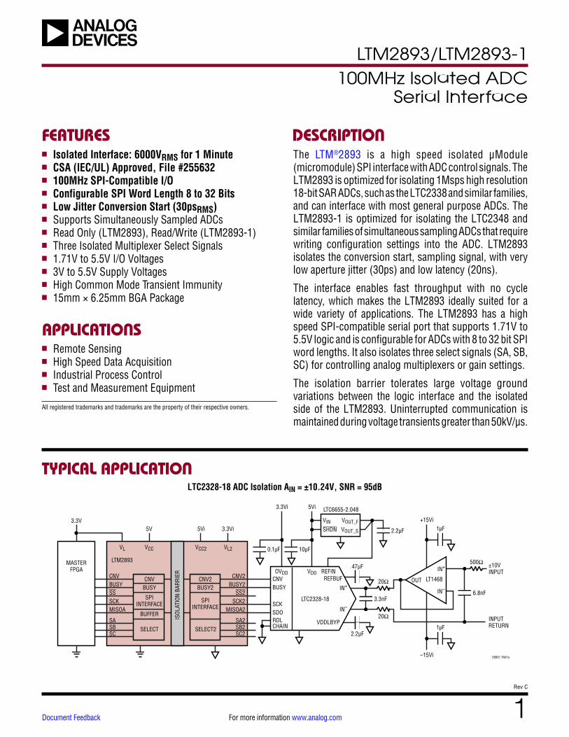
LTM2893/LTM2893-1 1 Rev C For more information www.analog.com Document Feedback TYPICAL APPLICATION FEATURES DESCRIPTION 100MHz Isolated ADC Serial Interface The LTM ® 2893 is a high speed isolated μModule (micromodule) SPI interface with ADC control signals. The LTM2893 is optimized for isolating 1Msps high resolution 18-bit SAR ADCs, such as the LTC2338 and similar families, and can interface with most general purpose ADCs. The LTM2893-1 is optimized for isolating the LTC2348 and similar families of simultaneous sampling ADCs that require writing configuration settings into the ADC. LTM2893 isolates the conversion start, sampling signal, with very low aperture jitter (30ps) and low latency (20ns). The interface enables fast throughput with no cycle latency, which makes the LTM2893 ideally suited for a wide variety of applications. The LTM2893 has a high speed SPI-compatible serial port that supports 1.71V to 5.5V logic and is configurable for ADCs with 8 to 32 bit SPI word lengths. It also isolates three select signals (SA, SB, SC) for controlling analog multiplexers or gain settings. The isolation barrier tolerates large voltage ground variations between the logic interface and the isolated side of the LTM2893. Uninterrupted communication is maintained during voltage transients greater than 50kV/µs. LTC2328-18 ADC Isolation A IN = ±10.24V, SNR = 95dB APPLICATIONS n Isolated Interface: 6000V RMS for 1 Minute n CSA (IEC/UL) Approved, File #255632 n 100MHz SPI-Compatible I/O n Configurable SPI Word Length 8 to 32 Bits n Low Jitter Conversion Start (30ps RMS ) n Supports Simultaneously Sampled ADCs n Read Only (LTM2893), Read/Write (LTM2893-1) n Three Isolated Multiplexer Select Signals n 1.71V to 5.5V I/O Voltages n 3V to 5.5V Supply Voltages n High Common Mode Transient Immunity n 15mm × 6.25mm BGA Package n Remote Sensing n High Speed Data Acquisition n Industrial Process Control n Test and Measurement Equipment LTM2893 V L V CC V L2 V CC2 CNV BUSY SS SCK MISOA SA SB SC SA2 SB2 SC2 CNV2 BUSY2 SS2 SCK2 MISOA2 CNV BUSY SPI INTERFACE BUFFER SELECT CNV2 BUSY2 SPI INTERFACE CNV BUSY SCK SDO RDL CHAIN V DD 5Vi 3.3Vi 5Vi 5V 3.3V 3.3Vi REFIN OV DD REFBUF VDDLBYP IN + IN – V IN SHDN V OUT_F V OUT_S 0.1μF 10μF 2.2μF 47μF 3.3nF IN + IN – OUT 2.2μF LTC2328-18 LTC6655-2.048 LT1468 6.8nF ±10V INPUT INPUT RETURN 500Ω 20Ω 20Ω MASTER FPGA 28931 TA01a 1μF +15Vi –15Vi ISOLATION BARRIER 1μF SELECT2 All registered trademarks and trademarks are the property of their respective owners.
Transcript of LTM2893/LTM2389-1 (Rev. C) - analog.com · cnv busy ss sck misoa sa sb sc sa2 sb2 sc2 cnv2 busy2...
LTM2893/LTM2893-1
1Rev C
For more information www.analog.comDocument Feedback
TYPICAL APPLICATION
FEATURES DESCRIPTION
100MHz Isolated ADCSerial Interface
The LTM®2893 is a high speed isolated μModule (micromodule) SPI interface with ADC control signals. The LTM2893 is optimized for isolating 1Msps high resolution 18-bit SAR ADCs, such as the LTC2338 and similar families, and can interface with most general purpose ADCs. The LTM2893-1 is optimized for isolating the LTC2348 and similar families of simultaneous sampling ADCs that require writing configuration settings into the ADC. LTM2893 isolates the conversion start, sampling signal, with very low aperture jitter (30ps) and low latency (20ns).
The interface enables fast throughput with no cycle latency, which makes the LTM2893 ideally suited for a wide variety of applications. The LTM2893 has a high speed SPI-compatible serial port that supports 1.71V to 5.5V logic and is configurable for ADCs with 8 to 32 bit SPI word lengths. It also isolates three select signals (SA, SB, SC) for controlling analog multiplexers or gain settings.
The isolation barrier tolerates large voltage ground variations between the logic interface and the isolated side of the LTM2893. Uninterrupted communication is maintained during voltage transients greater than 50kV/µs.
LTC2328-18 ADC Isolation AIN = ±10.24V, SNR = 95dB
APPLICATIONS
n Isolated Interface: 6000VRMS for 1 Minute n CSA (IEC/UL) Approved, File #255632 n 100MHz SPI-Compatible I/O n Configurable SPI Word Length 8 to 32 Bits n Low Jitter Conversion Start (30psRMS) n Supports Simultaneously Sampled ADCs n Read Only (LTM2893), Read/Write (LTM2893-1) n Three Isolated Multiplexer Select Signals n 1.71V to 5.5V I/O Voltages n 3V to 5.5V Supply Voltages n High Common Mode Transient Immunity n 15mm × 6.25mm BGA Package
n Remote Sensing n High Speed Data Acquisition n Industrial Process Control n Test and Measurement Equipment
LTM2893
VL VCC VL2VCC2
CNVBUSYSSSCKMISOA
SASBSC
SA2SB2SC2
CNV2BUSY2
SS2SCK2
MISOA2
CNVBUSY
SPIINTERFACE
BUFFER
SELECT
CNV2BUSY2
SPIINTERFACE
CNVBUSY
SCKSDORDLCHAIN
VDD
5Vi3.3Vi
5Vi5V3.3V
3.3Vi
REFINOVDDREFBUF
VDDLBYP
IN+
IN–
VIN
SHDN
VOUT_F
VOUT_S
0.1µF 10µF
2.2µF
47µF
3.3nF
IN+
IN–
OUT
2.2µF
LTC2328-18
LTC6655-2.048
LT1468
6.8nF
±10VINPUT
INPUTRETURN
500Ω
20Ω
20Ω
MASTERFPGA
28931 TA01a
1µF+15Vi
–15Vi
ISOL
ATIO
N BA
RRIE
R
1µFSELECT2
All registered trademarks and trademarks are the property of their respective owners.
LTM2893/LTM2893-1
2Rev C
For more information www.analog.com
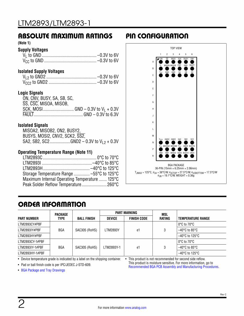
PIN CONFIGURATIONABSOLUTE MAXIMUM RATINGS
Supply Voltages VL to GND ................................................ –0.3V to 6V VCC to GND .............................................. –0.3V to 6V
Isolated Supply Voltages VL2 to GND2 ............................................ –0.3V to 6V VCC2 to GND2 .......................................... –0.3V to 6V
Logic Signals ON, CNV, BUSY, SA, SB, SC, SS, CSC, MISOA, MISOB, SCK, MOSI ........................... GND – 0.3V to VL + 0.3V FAULT ........................................... GND – 0.3V to 6.3V
Isolated Signals MISOA2, MISOB2, ON2, BUSY2, BUSYS, MOSI2, CNV2, SCK2, SS2, SA2, SB2, SC2 ..................GND2 – 0.3V to VL2 + 0.3V
Operating Temperature Range (Note 11) LTM2893C ............................................... 0°C to 70°C LTM2893I ............................................–40°C to 85°C LTM2893H ......................................... –40°C to 125°C Storage Temperature Range .............. –55°C to 125°C Maximum Internal Operating Temperature ....... 125°C Peak Solder Reflow Temperature ...................... 260°C
(Note 1)
BGA PACKAGE36-PIN (15mm × 6.25mm × 2.06mm)
TJMAX = 125°C, θJA = 36°C/W, θJCTOP = 27.5°C/W, θJCBOTTOM = 17.5°C/WθJB = 19.1°C/W, WEIGHT = 0.36g
TOP VIEW
R
P
N
M
L
K
J
H
G
F
E
D
C
B
A
1 2 3 4 5 6
CNV
FAULT
SC
SCK
CSC
SA
BUSY
SB
GND
MOSI
GND
MISOB
SS
GND
MISOA
ON
VCC
VL
SC2
BUSYS
CNV2
SA2
VL2
SCK2
SB2
BUSY2
GND2
GND2
MOSI2
MISOB2
GND2
SS2
MISOA2
VCC2
ON2
VL2
ORDER INFORMATION
PART NUMBERPACKAGE
TYPE BALL FINISH
PART MARKING MSL RATING TEMPERATURE RANGEDEVICE FINISH CODE
LTM2893CY#PBF
BGA SAC305 (RoHS) LTM2893Y e1 3
0°C to 70°C
LTM2893IY#PBF –40°C to 85°C
LTM2893HY#PBF –40°C to 125°C
LTM2893CY-1#PBF
BGA SAC305 (RoHS) LTM2893Y-1 e1 3
0°C to 70°C
LTM2893IY-1#PBF –40°C to 85°C
LTM2893HY-1#PBF –40°C to 125°C
• Device temperature grade is indicated by a label on the shipping container.
• Pad or ball finish code is per IPC/JEDEC J-STD-609.• BGA Package and Tray Drawings
• This product is not recommended for second side reflow. This product is moisture sensitive. For more information, go to Recommended BGA PCB Assembly and Manufacturing Procedures.

LTM2893/LTM2893-1
3Rev C
For more information www.analog.com
ELECTRICAL CHARACTERISTICS The l denotes the specifications which apply over the full specified operating temperature range, otherwise specifications are at TA = 25°C. VCC = 5V, VL = 3.3V, GND = 0V, VCC2 = 5V, VL2 = 3.3V, GND2 = 0V unless otherwise noted. (Note 9)
SYMBOL PARAMETER CONDITIONS MIN TYP MAX UNITS
Power Supplies
VCC Operating Supply Range l 3.0 5.5 V
ICC Operating Supply Current Idle l 9 12 mA
Operating Supply Current 1Msps, ADC Conversion Rate
20pF Loads, SCK = 100MHz l 12 15 mA
VCC2 Isolated Operating Supply Range l 3.0 5.5 V
ICC2 Isolated Operating Supply Current Idle l 9 12 mA
Isolated Operating Supply Current, 1Msps ADC Conversion Rate
20pF Loads, SCK2 = 100MHz l 12 15 mA
VL Logic Interface Supply Range l 1.71 5.5 V
IL Logic Interface Supply Current Inputs and Outputs Static at GND or VL l ±200 µA
Logic Interface Supply Current, 1Msps Conversion Rate
SCK = 100MHz, 20pF Load l 2 5 mA
VL2 Isolated Interface Supply Range l 1.71 5.5 V
IL2 Isolated Interface Supply Current Inputs and Outputs Static at GND2 or VL2 l ±200 µA
Isolated Interface Supply Current, 1Msps ADC Conversion Rate
SCK2 = 100MHz, 20pF Load l 2.5 5 mA
Digital Inputs and Digital Outputs (Logic Side)
VIH High Level Input Voltage 1.71V ≤ VL ≤ 5.5V l 0.8 • VL V
VIL Low Level Input Voltage 1.71V ≤ VL ≤ 5.5V l 0.2 • VL V
Digital Input Current (MOSI, SCK, CNV) VIN = 0V to VL l ±1 µA
Digital Input Current (SS, CSC, SA, SB, SC, ON) VIN = 0V to VL l ±60 µA
Digital Input Capacitance Note 2 5 pF
VOH High Level Output Voltage IOUT = –500µA, 1.71V ≤ VL ≤ 5.5V l VL – 0.2 V
VOL Low Level Output Voltage IOUT = 500µA, 1.71V ≤ VL ≤ 5.5V l 0.2 V
IOZ High-Z Output Leakage Current MISOA, MISOB SS = VL l ±1 µA
Output Source Current (Short-Circuit) VOUT = 0V (Note 2) –80 mA
Output Sink Current (Short-Circuit) VOUT = VL (Note 2) 80 mA
Digital Inputs and Digital Outputs (Isolated Side)
VIH High Level Input Voltage 1.71V ≤ VL2 ≤ 5.5V l 0.8 • VL2 V
VIL Low Level Input Voltage 1.71V ≤ VL2 ≤ 5.5V l 0.2 • VL2 V
Digital Input Current (ON2, BUSY2, BUSYS) VIN = 0V to VL2, ON2 = VL2 l ±60 µA
Digital Input Current (MISOA2, MISOB2) VIN = 0V to VL2 l ±10 µA
Digital Input Capacitance Note 2 5 pF
VOH High Level Output Voltage IOUT = –500µA, 1.71V ≤ VL2 ≤ 5.5V l VL2 – 0.2 V
VOL Low Level Output Voltage IOUT = 500µA, 1.71V ≤ VL2 ≤ 5.5V l 0.2 V
Output Source Current (Short-Circuit) VOUT = 0V (Note 2) –80 mA
Output Sink Current (Short-Circuit) VOUT = VL2 (Note 2) 80 mA
ESD Performance (Note 7)
Isolation Barrier Logic Side I/O Pins Isolated Side I/O Pins
From GND, VL, or VCC to GND2, VL2, or VCC2 With Respect to GND, VL, or VCC With Respect to GND2, VL2, or VCC2
±15 ±4 ±4
kV kV kV
LTM2893/LTM2893-1
4Rev C
For more information www.analog.com
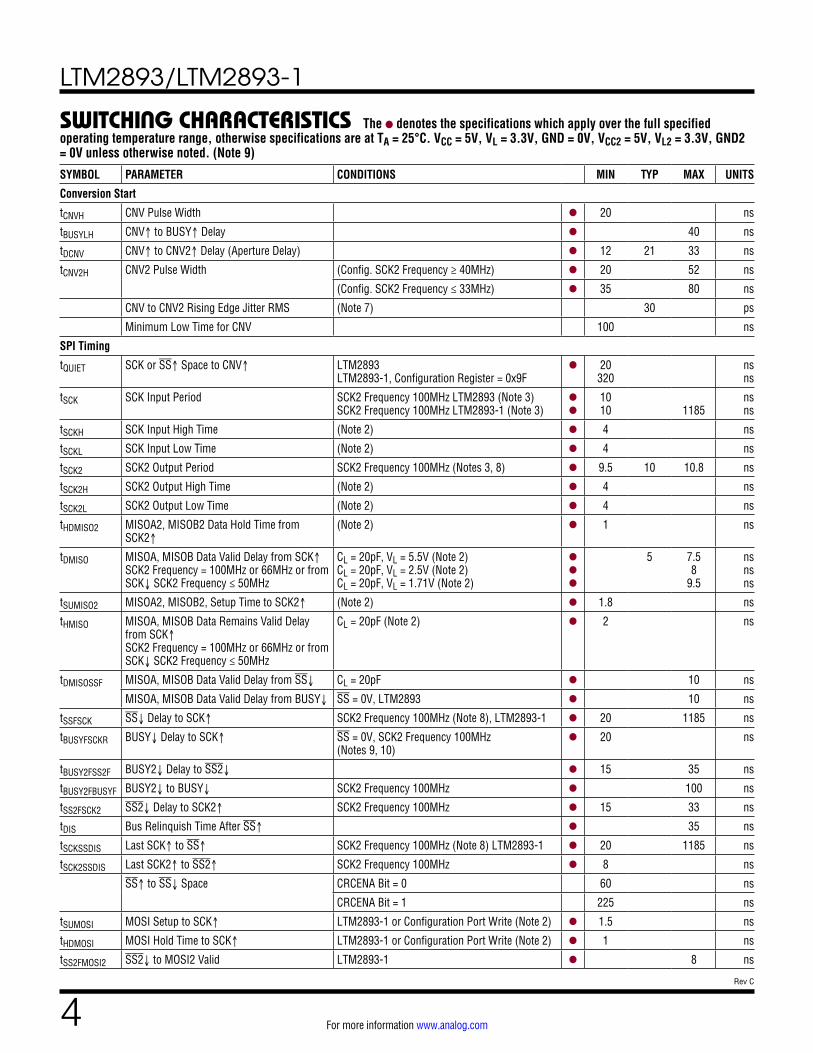
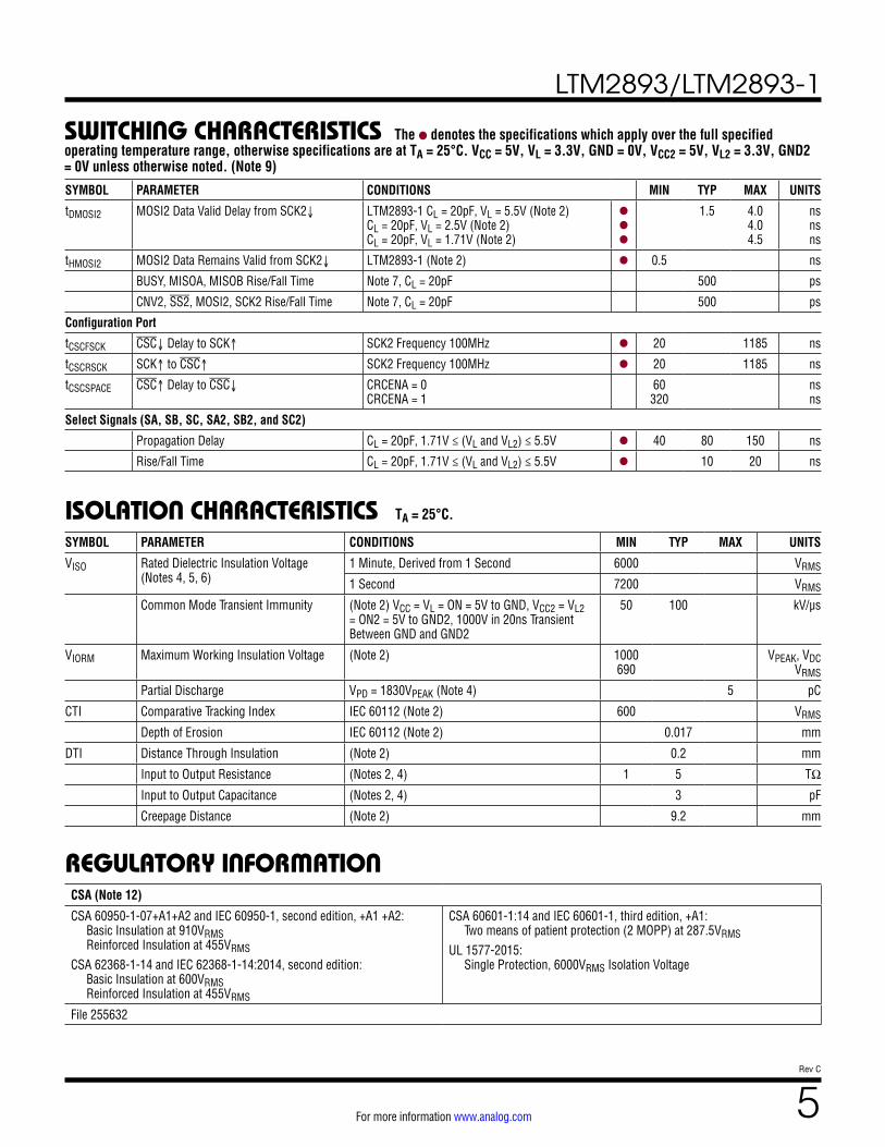
SWITCHING CHARACTERISTICS The l denotes the specifications which apply over the full specified operating temperature range, otherwise specifications are at TA = 25°C. VCC = 5V, VL = 3.3V, GND = 0V, VCC2 = 5V, VL2 = 3.3V, GND2 = 0V unless otherwise noted. (Note 9)
SYMBOL PARAMETER CONDITIONS MIN TYP MAX UNITS
Conversion Start
tCNVH CNV Pulse Width l 20 ns
tBUSYLH CNV↑ to BUSY↑ Delay l 40 ns
tDCNV CNV↑ to CNV2↑ Delay (Aperture Delay) l 12 21 33 ns
tCNV2H CNV2 Pulse Width (Config. SCK2 Frequency ≥ 40MHz) l 20 52 ns
(Config. SCK2 Frequency ≤ 33MHz) l 35 80 ns
CNV to CNV2 Rising Edge Jitter RMS (Note 7) 30 ps
Minimum Low Time for CNV 100 ns
SPI Timing
tQUIET SCK or SS↑ Space to CNV↑ LTM2893 LTM2893-1, Configuration Register = 0x9F
l 20 320
ns ns
tSCK SCK Input Period SCK2 Frequency 100MHz LTM2893 (Note 3) SCK2 Frequency 100MHz LTM2893-1 (Note 3)
l
l
10 10
1185
ns ns
tSCKH SCK Input High Time (Note 2) l 4 ns
tSCKL SCK Input Low Time (Note 2) l 4 ns
tSCK2 SCK2 Output Period SCK2 Frequency 100MHz (Notes 3, 8) l 9.5 10 10.8 ns
tSCK2H SCK2 Output High Time (Note 2) l 4 ns
tSCK2L SCK2 Output Low Time (Note 2) l 4 ns
tHDMISO2 MISOA2, MISOB2 Data Hold Time from SCK2↑
(Note 2) l 1 ns
tDMISO MISOA, MISOB Data Valid Delay from SCK↑ SCK2 Frequency = 100MHz or 66MHz or from SCK↓ SCK2 Frequency ≤ 50MHz
CL = 20pF, VL = 5.5V (Note 2) CL = 20pF, VL = 2.5V (Note 2) CL = 20pF, VL = 1.71V (Note 2)
l
l
l
5 7.5 8
9.5
ns ns ns
tSUMISO2 MISOA2, MISOB2, Setup Time to SCK2↑ (Note 2) l 1.8 ns
tHMISO MISOA, MISOB Data Remains Valid Delay from SCK↑ SCK2 Frequency = 100MHz or 66MHz or from SCK↓ SCK2 Frequency ≤ 50MHz
CL = 20pF (Note 2) l 2 ns
tDMISOSSF MISOA, MISOB Data Valid Delay from SS↓ CL = 20pF l 10 ns
MISOA, MISOB Data Valid Delay from BUSY↓ SS = 0V, LTM2893 l 10 ns
tSSFSCK SS↓ Delay to SCK↑ SCK2 Frequency 100MHz (Note 8), LTM2893-1 l 20 1185 ns
tBUSYFSCKR BUSY↓ Delay to SCK↑ SS = 0V, SCK2 Frequency 100MHz (Notes 9, 10)
l 20 ns
tBUSY2FSS2F BUSY2↓ Delay to SS2↓ l 15 35 ns
tBUSY2FBUSYF BUSY2↓ to BUSY↓ SCK2 Frequency 100MHz l 100 ns
tSS2FSCK2 SS2↓ Delay to SCK2↑ SCK2 Frequency 100MHz l 15 33 ns
tDIS Bus Relinquish Time After SS↑ l 35 ns
tSCKSSDIS Last SCK↑ to SS↑ SCK2 Frequency 100MHz (Note 8) LTM2893-1 l 20 1185 ns
tSCK2SSDIS Last SCK2↑ to SS2↑ SCK2 Frequency 100MHz l 8 ns
SS↑ to SS↓ Space CRCENA Bit = 0 60 ns
CRCENA Bit = 1 225 ns
tSUMOSI MOSI Setup to SCK↑ LTM2893-1 or Configuration Port Write (Note 2) l 1.5 ns
tHDMOSI MOSI Hold Time to SCK↑ LTM2893-1 or Configuration Port Write (Note 2) l 1 ns
tSS2FMOSI2 SS2↓ to MOSI2 Valid LTM2893-1 l 8 ns
LTM2893/LTM2893-1
5Rev C
For more information www.analog.com
SWITCHING CHARACTERISTICS The l denotes the specifications which apply over the full specified operating temperature range, otherwise specifications are at TA = 25°C. VCC = 5V, VL = 3.3V, GND = 0V, VCC2 = 5V, VL2 = 3.3V, GND2 = 0V unless otherwise noted. (Note 9)
SYMBOL PARAMETER CONDITIONS MIN TYP MAX UNITS
tDMOSI2 MOSI2 Data Valid Delay from SCK2↓ LTM2893-1 CL = 20pF, VL = 5.5V (Note 2) CL = 20pF, VL = 2.5V (Note 2) CL = 20pF, VL = 1.71V (Note 2)
l
l
l
1.5 4.0 4.0 4.5
ns ns ns
tHMOSI2 MOSI2 Data Remains Valid from SCK2↓ LTM2893-1 (Note 2) l 0.5 ns
BUSY, MISOA, MISOB Rise/Fall Time Note 7, CL = 20pF 500 ps
CNV2, SS2, MOSI2, SCK2 Rise/Fall Time Note 7, CL = 20pF 500 ps
Configuration Port
tCSCFSCK CSC↓ Delay to SCK↑ SCK2 Frequency 100MHz l 20 1185 ns
tCSCRSCK SCK↑ to CSC↑ SCK2 Frequency 100MHz l 20 1185 ns
tCSCSPACE CSC↑ Delay to CSC↓ CRCENA = 0 CRCENA = 1
60 320
ns ns
Select Signals (SA, SB, SC, SA2, SB2, and SC2)
Propagation Delay CL = 20pF, 1.71V ≤ (VL and VL2) ≤ 5.5V l 40 80 150 ns
Rise/Fall Time CL = 20pF, 1.71V ≤ (VL and VL2) ≤ 5.5V l 10 20 ns
SYMBOL PARAMETER CONDITIONS MIN TYP MAX UNITS
VISO Rated Dielectric Insulation Voltage (Notes 4, 5, 6)
1 Minute, Derived from 1 Second 6000 VRMS
1 Second 7200 VRMS
Common Mode Transient Immunity (Note 2) VCC = VL = ON = 5V to GND, VCC2 = VL2 = ON2 = 5V to GND2, 1000V in 20ns Transient Between GND and GND2
50 100 kV/µs
VIORM Maximum Working Insulation Voltage (Note 2) 1000 690
VPEAK, VDC VRMS
Partial Discharge VPD = 1830VPEAK (Note 4) 5 pC
CTI Comparative Tracking Index IEC 60112 (Note 2) 600 VRMS
Depth of Erosion IEC 60112 (Note 2) 0.017 mm
DTI Distance Through Insulation (Note 2) 0.2 mm
Input to Output Resistance (Notes 2, 4) 1 5 TΩ
Input to Output Capacitance (Notes 2, 4) 3 pF
Creepage Distance (Note 2) 9.2 mm
CSA (Note 12)
CSA 60950-1-07+A1+A2 and IEC 60950-1, second edition, +A1 +A2: Basic Insulation at 910VRMS Reinforced Insulation at 455VRMS
CSA 62368-1-14 and IEC 62368-1-14:2014, second edition: Basic Insulation at 600VRMS Reinforced Insulation at 455VRMS
CSA 60601-1:14 and IEC 60601-1, third edition, +A1: Two means of patient protection (2 MOPP) at 287.5VRMS
UL 1577-2015: Single Protection, 6000VRMS Isolation Voltage
File 255632
ISOLATION CHARACTERISTICS
REGULATORY INFORMATION
TA = 25°C.
LTM2893/LTM2893-1
6Rev C
For more information www.analog.com
ELECTRICAL CHARACTERISTICS
tDELAY
0.8 •VL or 0.8 •VL2
0.2 •VL or 0.2 •VL2
tDELAY
tWIDTH
2893 F01
0.8 •VL or 0.8 •VL20.2•VL or 0.2•VL2
0.8 •VL or 0.8 •VL2
0.5•VL or0.5•VL2
0.2•VL or 0.2•VL2
Figure 1. Voltage Levels for Timing Specifications
TYPICAL PERFORMANCE CHARACTERISTICS
SNR vs fIN for 30psRMS CNV JitterCNV → CNV2 Delay vs Temperature CNV → CNV2 Delay vs VL and VL2
Specifications are at TA = 25°C. VCC = 5V, VL = 3.3V, GND = 0V, VCC2 = 5V, VL2 = 5.0V, GND2 = 0V, unless otherwise noted.
100dB96dB84dB
72dB60dB
FREQUENCY (Hz)1k 10k 100k 1M
40
50
60
70
80
90
100
110
120
SNR
(dB)
2893 G01TEMPERATURE (°C)
–60 –40 –20 0 20 40 60 80 100 120 14015
16
17
18
19
20
21
22
23
24
25
DELA
Y (n
s)
2893 G02VL AND VL2 (V)
1.5 2 2.5 3 3.5 4 4.5 5 5.515
16
17
18
19
20
21
22
23
24
25
DELA
Y (n
s)
2893 G03
Note 1: Stresses beyond those listed under Absolute Maximum Ratings may cause permanent damage to the device. Exposure to any Absolute Maximum Rating condition for extended periods may affect device reliability and lifetime.Note 2: Guaranteed by design, not production tested.Note 3: Guaranteed by other measured parameters and is not directly tested. Note 4: Device considered a 2-terminal device. Measurement between groups of pins A1 through C6 shorted together and pins N1 through R6 shorted together. Note 5: The rated dielectric insulation voltage should not be interpreted as a continuous voltage rating.Note 6: In accordance with UL1577, each device is proof tested for the 6000VRMS rating by applying an RMS voltage multiplied by an acceleration factor of 1.2 for one second.
Note 7: Evaluated by Design, not production tested.Note 8: See Table 5 for minimum and maximum timing specifications affected by the selection of SCK2 frequencies in the configuration register. Note 9: All currents into device pins are positive; all currents out of device are negative. All voltages are referenced to their corresponding ground unless otherwise specified.Note 10: See Table 2 for delay requirements between falling edge of BUSY and SCK for large word lengths.Note 11: Continuous operation above specified maximum operating junction temperature may result in device degradation or failure. Note 12: Ratings are for pollution degree 2, material group 3 and overvoltage category II where applicable. Ratings for other environmental and electrical conditions to be determined from the appropriate safety standard.
LTM2893/LTM2893-1
7Rev C
For more information www.analog.com
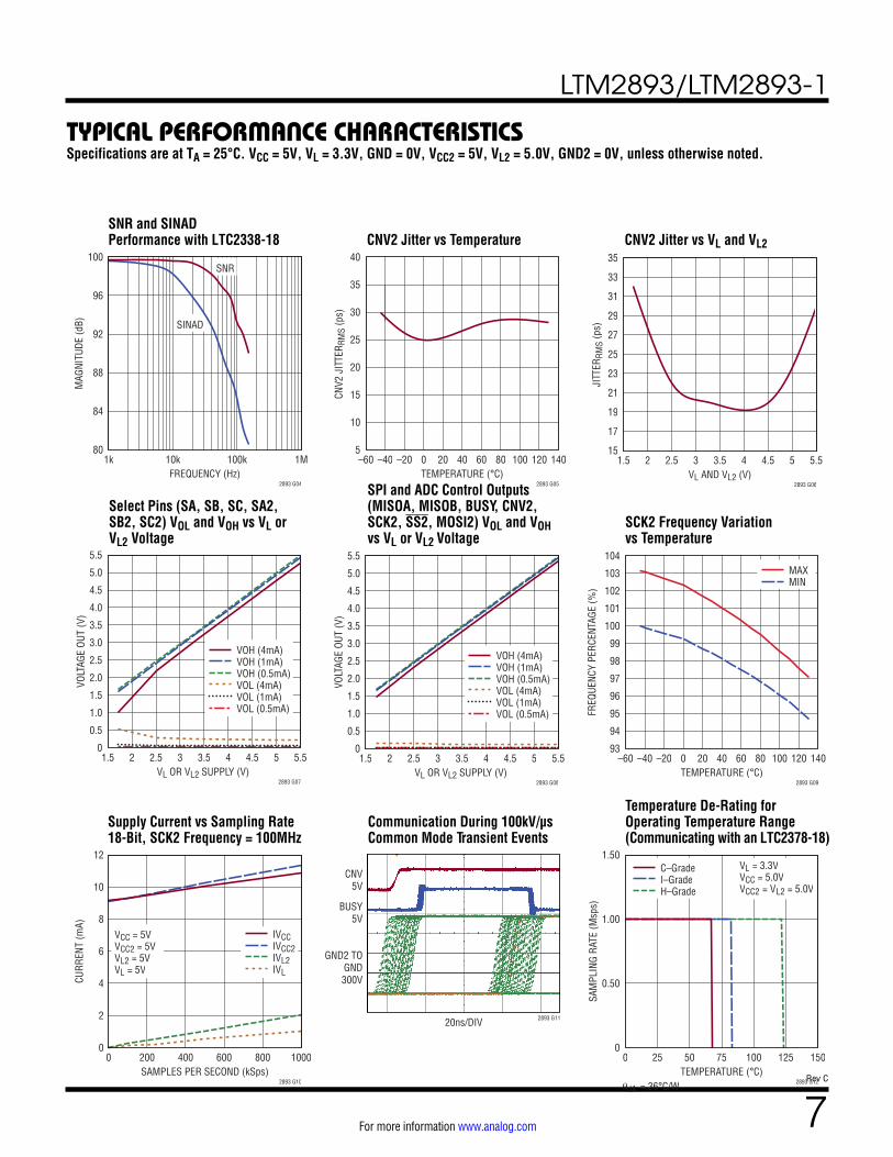
SNR and SINADPerformance with LTC2338-18 CNV2 Jitter vs Temperature CNV2 Jitter vs VL and VL2
Select Pins (SA, SB, SC, SA2, SB2, SC2) VOL and VOH vs VL or VL2 Voltage
SPI and ADC Control Outputs (MISOA, MISOB, BUSY, CNV2, SCK2, SS2, MOSI2) VOL and VOH vs VL or VL2 Voltage
SCK2 Frequency Variation vs Temperature
TYPICAL PERFORMANCE CHARACTERISTICSSpecifications are at TA = 25°C. VCC = 5V, VL = 3.3V, GND = 0V, VCC2 = 5V, VL2 = 5.0V, GND2 = 0V, unless otherwise noted.
Supply Current vs Sampling Rate 18-Bit, SCK2 Frequency = 100MHz
Communication During 100kV/µs Common Mode Transient Events
Temperature De-Rating for Operating Temperature Range (Communicating with an LTC2378-18)
VOH (4mA)VOH (1mA)VOH (0.5mA)VOL (4mA)VOL (1mA)VOL (0.5mA)
VL OR VL2 SUPPLY (V)1.5 2 2.5 3 3.5 4 4.5 5 5.5
0
0.5
1.0
1.5
2.0
2.5
3.0
3.5
4.0
4.5
5.0
5.5
VOLT
AGE
OUT
(V)
2893 G07
VOH (4mA)VOH (1mA)VOH (0.5mA)VOL (4mA)VOL (1mA)VOL (0.5mA)
VL OR VL2 SUPPLY (V)1.5 2 2.5 3 3.5 4 4.5 5 5.5
0
0.5
1.0
1.5
2.0
2.5
3.0
3.5
4.0
4.5
5.0
5.5
VOLT
AGE
OUT
(V)
2893 G08
MAXMIN
TEMPERATURE (°C)–60 –40 –20 0 20 40 60 80 100 120 140
93
94
95
96
97
98
99
100
101
102
103
104
FREQ
UENC
Y PE
RCEN
TAGE
(%)
2893 G09
SNR
SINAD
FREQUENCY (Hz)1k 10k 100k 1M
80
84
88
92
96
100
MAG
NITU
DE (d
B)
2893 G04TEMPERATURE (°C)
–60 –40 –20 0 20 40 60 80 100 120 1405
10
15
20
25
30
35
40
CNV2
JIT
TER R
MS
(ps)
2893 G05VL AND VL2 (V)
1.5 2 2.5 3 3.5 4 4.5 5 5.515
17
19
21
23
25
27
29
31
33
35
JITT
ERRM
S (p
s)
2893 G06
VCC = 5V VCC2 = 5V VL2 = 5V VL = 5V
IVCCIVCC2IVL2IVL
SAMPLES PER SECOND (kSps)0 200 400 600 800 1000
0
2
4
6
8
10
12
CURR
ENT
(mA)
2893 G10
VL = 3.3VVCC = 5.0VVCC2 = VL2 = 5.0V
θJA = 36°C/W
C–GradeI–GradeH–Grade
TEMPERATURE (°C)0 25 50 75 100 125 150
0
0.50
1.00
1.50
SAM
PLIN
G RA
TE (M
sps)
2893 G12
20ns/DIV
GND2 TOGND300V
BUSY5V
CNV5V
2893 G11
LTM2893/LTM2893-1
8Rev C
For more information www.analog.com
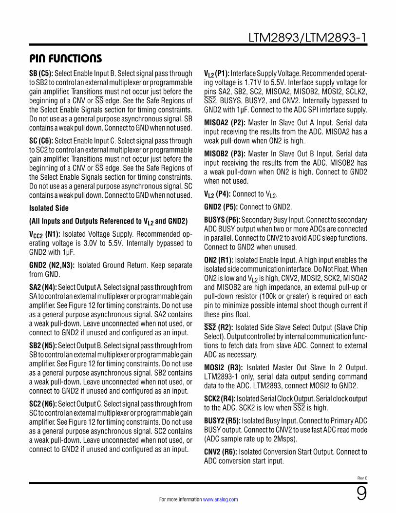
PIN FUNCTIONSLogic Side
(All Inputs and Outputs Referenced to VL and GND)
ON (A1): Enable Input. A high input enables the logic side. When ON is low and VL is high, MOSI, SCK, CNV, MISOA, and MISOB are high impedance, an external pull-up or pull-down resistor (100k or greater) is required on each pin to minimize possible internal shoot though current if these pins float.
SS (A2): Slave Select Input (Low True Slave Chip Select). A low on the SS input enables MISOA and MISOB. To clear faults or write the configuration register the SS input must be high. With the LTM2893, the SS input may remain low between ADC reads. With the LTM2893-1, the SS input must frame the SCK transitions and not exceed the defined watchdog timeouts. The SS pin contains a weak pull up to the VL supply. CSC must be high for SS to be enabled.
MOSI (A3): Master Out Slave In Input. MOSI is the serial data input for the configuration registers or input for se-rial data to be written to the isolated ADC through MOSI2, (LTM2893-1 option). When MOSI is not used, MOSI should be connected to GND. Connect a weak pull-up to VL or a weak pull-down to GND to maintain a valid logic input when MOSI is not driven.
SCK (A4): Serial Port Clock Input. MISOA and MISOB data change after a rising edge of the SCK input. MOSI data is read in on the rising edge of the SCK input. Connect a weak pull-up to VL or a weak pull-down to GND to maintain a valid logic input when SCK is not driven.
BUSY (A5): Busy Output. A high output indicates the ADC is currently converting a result. On the falling edge of the BUSY output the data is ready to be read out of the serial digital interface. At startup, a high on the BUSY output indicates the isolated side is not ready. Once the BUSY output goes low the system is ready.
CNV (A6): Conversion Start Input. The rising edge of CNV is transferred to CNV2 with minimal delay and minimal jitter. Do not change the CNV input during a read of the serial digital interface. The falling edge of CNV is ignored.
VL (B1): Interface Logic Supply. Recommended operating voltage is 1.71V to 5.5V. Interface supply voltage for pins SA, SB, SC, MISOA, MISOB, MOSI, SCLK, SS, CSC, BUSY, and CNV. Internally bypassed to GND with 1µF.
MISOA (B2): Master In Slave Out A Output. Serial data output containing the ADC result from MISOA2. Connect a weak pull-up to VL or a weak pull-down to GND to maintain a valid logic level when MISOA is high impedance while SS is high.
MISOB (B3): Master In Slave Out B Output. Serial data output containing the ADC results from MISOB2. Con-nect a weak pull-up to VL or a weak pull-down to GND to maintain a valid logic level when MISOB is high impedance while SS is high..
CSC (B4): Chip Select Configuration Input (CSC Chip Select). A low on the CSC input enables access to the configuration register. The Configuration Register section describes configurable options. SS must be high for CSC to be enabled.
GND (B5): Connect to GND.
FAULT (B6): Fault Output Open Drain. A low on the FAULT output indicates a communication or command error. Connect to an external 4.7k pull-up to VL to monitor fault events.
VCC (C1): Supply Voltage. Recommended operating volt-age is 3.0V to 5.5V. Internally bypassed to GND with 1µF.
GND (C2-C3): Circuit Ground. Return for VL logic supply and VCC supply.
SA (C4): Select Enable Input A. Select signal pass through to SA2 to control an external multiplexer or programmable gain amplifier. Transitions must not occur just before the beginning of a CNV or SS edge. See the Safe Regions of the Select Enable Signals section for timing constraints. Do not use as a general purpose asynchronous signal. SA contains a weak pull down. Connect to GND when not used.
LTM2893/LTM2893-1
9Rev C
For more information www.analog.com
SB (C5): Select Enable Input B. Select signal pass through to SB2 to control an external multiplexer or programmable gain amplifier. Transitions must not occur just before the beginning of a CNV or SS edge. See the Safe Regions of the Select Enable Signals section for timing constraints. Do not use as a general purpose asynchronous signal. SB contains a weak pull down. Connect to GND when not used.
SC (C6): Select Enable Input C. Select signal pass through to SC2 to control an external multiplexer or programmable gain amplifier. Transitions must not occur just before the beginning of a CNV or SS edge. See the Safe Regions of the Select Enable Signals section for timing constraints. Do not use as a general purpose asynchronous signal. SC contains a weak pull down. Connect to GND when not used.
Isolated Side
(All Inputs and Outputs Referenced to VL2 and GND2)
VCC2 (N1): Isolated Voltage Supply. Recommended op-erating voltage is 3.0V to 5.5V. Internally bypassed to GND2 with 1µF.
GND2 (N2,N3): Isolated Ground Return. Keep separate from GND.
SA2 (N4): Select Output A. Select signal pass through from SA to control an external multiplexer or programmable gain amplifier. See Figure 12 for timing constraints. Do not use as a general purpose asynchronous signal. SA2 contains a weak pull-down. Leave unconnected when not used, or connect to GND2 if unused and configured as an input.
SB2 (N5): Select Output B. Select signal pass through from SB to control an external multiplexer or programmable gain amplifier. See Figure 12 for timing constraints. Do not use as a general purpose asynchronous signal. SB2 contains a weak pull-down. Leave unconnected when not used, or connect to GND2 if unused and configured as an input.
SC2 (N6): Select Output C. Select signal pass through from SC to control an external multiplexer or programmable gain amplifier. See Figure 12 for timing constraints. Do not use as a general purpose asynchronous signal. SC2 contains a weak pull-down. Leave unconnected when not used, or connect to GND2 if unused and configured as an input.
PIN FUNCTIONSVL2 (P1): Interface Supply Voltage. Recommended operat-ing voltage is 1.71V to 5.5V. Interface supply voltage for pins SA2, SB2, SC2, MISOA2, MISOB2, MOSI2, SCLK2, SS2, BUSYS, BUSY2, and CNV2. Internally bypassed to GND2 with 1µF. Connect to the ADC SPI interface supply.
MISOA2 (P2): Master In Slave Out A Input. Serial data input receiving the results from the ADC. MISOA2 has a weak pull-down when ON2 is high.
MISOB2 (P3): Master In Slave Out B Input. Serial data input receiving the results from the ADC. MISOB2 has a weak pull-down when ON2 is high. Connect to GND2 when not used.
VL2 (P4): Connect to VL2.
GND2 (P5): Connect to GND2.
BUSYS (P6): Secondary Busy Input. Connect to secondary ADC BUSY output when two or more ADCs are connected in parallel. Connect to CNV2 to avoid ADC sleep functions. Connect to GND2 when unused.
ON2 (R1): Isolated Enable Input. A high input enables the isolated side communication interface. Do Not Float. When ON2 is low and VL2 is high, CNV2, MOSI2, SCK2, MISOA2 and MISOB2 are high impedance, an external pull-up or pull-down resistor (100k or greater) is required on each pin to minimize possible internal shoot though current if these pins float.
SS2 (R2): Isolated Side Slave Select Output (Slave Chip Select). Output controlled by internal communication func-tions to fetch data from slave ADC. Connect to external ADC as necessary.
MOSI2 (R3): Isolated Master Out Slave In 2 Output. LTM2893-1 only, serial data output sending command data to the ADC. LTM2893, connect MOSI2 to GND2.
SCK2 (R4): Isolated Serial Clock Output. Serial clock output to the ADC. SCK2 is low when SS2 is high.
BUSY2 (R5): Isolated Busy Input. Connect to Primary ADC BUSY output. Connect to CNV2 to use fast ADC read mode (ADC sample rate up to 2Msps).
CNV2 (R6): Isolated Conversion Start Output. Connect to ADC conversion start input.
LTM2893/LTM2893-1
10Rev C
For more information www.analog.com
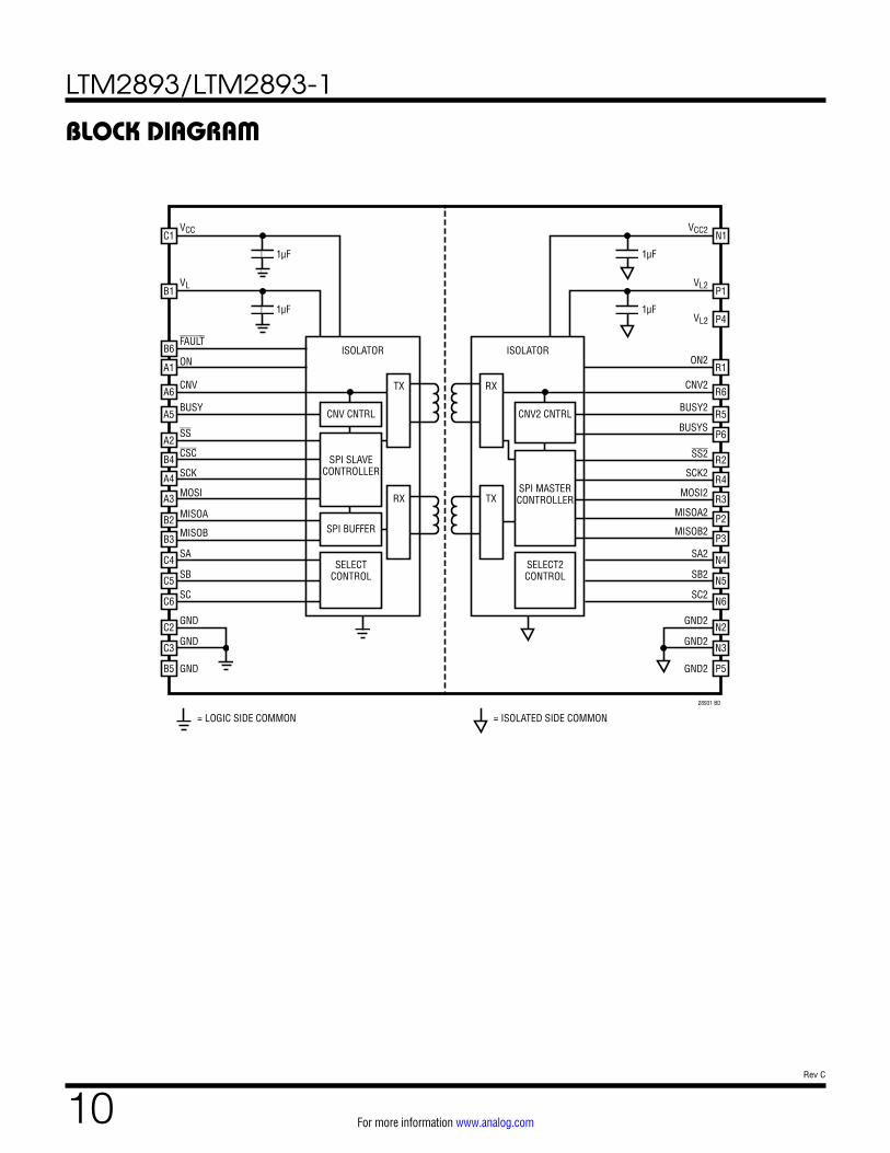
BLOCK DIAGRAM
28931 BD
SPI BUFFER
SELECTCONTROL
SPI SLAVECONTROLLER
TX
RX
CNV CNTRL
ISOLATOR
SELECT2CONTROL
SPI MASTERCONTROLLER
RX
TX
CNV2 CNTRL
ISOLATOR
1µF
1µF
VCC
VL
ON
CNV
BUSY
SS
CSC
SCK
MOSI
MISOA
MISOB
SA
SB
SC
GND
GND
GND
FAULT
VCC2
VL2
ON2
CNV2
BUSY2
BUSYS
SS2
SCK2
MOSI2
MISOA2
MISOB2
SA2
SB2
SC2
GND2
GND2
GND2
1µF
1µF
C1
B1
N1
P1
VL2 P4
B6
A1 R1
A6
A5
A2
B4
A4
A3
B2
B3
C6
C5
C4
N6
N5
N4
B5
C3
C2
P6
P5
N3
N2
R2
R4
R3
P2
P3
R6
R5
= LOGIC SIDE COMMON = ISOLATED SIDE COMMON
LTM2893/LTM2893-1
11Rev C
For more information www.analog.com
APPLICATIONS INFORMATIONOVERVIEW
The LTM2893 contains the functions to communicate with analog to digital converters (ADC) using a fast SPI interface. The LTM2893 utilizes state machines and SPI buffers to manage the ADC-specific operations. An inde-pendent configuration chip select (CSC) allows selection of the SCK frequency, word length, device count, and select signal direction to tailor the operation to a specific ADC. See ADC Requirements for a list of compatibility-tested Analog Devices ADCs.
The LTM2893 follows the signal flow of a standard SAR ADC interface. The process is initiated by the rising edge of the CNV input signal. A high on the BUSY signal follows and the CNV start edge is transferred to the isolated ADC through the CNV2 output. The isolated side waits for the ADC’s busy signal, connected to BUSY2, to go high then low. At the falling edge of BUSY2, the isolated side will access the ADC’s SPI port and read out the result and transfer it to the logic side, where it is stored in a buffer. When the buffer has data, the logic side BUSY signal will release and the MISOA, MISOB ports are ready to be read. The ADC SPI isolator adds a small delay to the process of an overall ADC cycle. The small delay, approximately 80ns, is observed as a difference in the length of the BUSY and BUSY2 signals.
ISOLATOR µMODULE TECHNOLOGY
The LTM2893 utilizes isolator μModule technology to trans-late signals across an isolation barrier. Signals on either side of the barrier are encoded into pulses and translated across the isolation boundary using differential signaling through coreless transformers formed in the μModule substrate. This system, complete with error checking, safe shutdown on fail, and extremely high common mode im-munity, provides a robust solution for bidirectional signal isolation. The μModule technology provides the means to combine the isolated signaling with our SPI transceiver in one small package.
ADC REQUIREMENTS
Ideally Suited ADI ADCs:
LTM2893n LTC2380/LTC2379/LTC2378/LTC2377/LTC2376n LTC2338/LTC2337/LTC2336n LTC2328/LTC2327/LTC2326n LTC2370/LTC2369/LTC2368/LTC2367/LTC2364n LTC2383/LTC2382/LTC2381
LTM2893-1n LTC2348/LTC2345
The following requirements should be met for other ADCs to be compatible with the LTM2893:n 6.25MHz ≤ SPI shift clock maximum frequency ≤
100MHzn Operates in SPI mode (0,0): SCK starts low, data cap-
tured on rising edge.n Meets setup and hold timing requirements (tHDMISO2
and tSUMISO2) with the SPI shift clock operating between 6.25MHz and 100MHz.
n SPI shift clock (SCK) is static outside of CS (the ADC does not require a constant running SCK as a conver-sion clock)
n If used, the conversion start pulse width minimum is ≤ tCNVH
The following requirements should be met for other ADCs to be compatible with the LTM2893-1 in addition to the LTM2893 requirements:n The ADC write data is a second transaction. The first
transaction reads the ADC result. A second transaction writes the data received into the MOSI pin when the ADC result is read from the LTM2893.
LTM2893/LTM2893-1
12Rev C
For more information www.analog.com
APPLICATIONS INFORMATIONThe SPI bus lacks a formal standard, and therefore, various implementations of protocol, bit lengths, and signal polari-ties exist. In the universe of analog-to-digital converters (ADCs) with serial peripheral interfaces (SPI), a nominal set of requirements must be met to operate properly with the LTM2893.
First, the LTM2893 operates similar to mode (0, 0). The data is captured and shifted on the rising edge of SCK. All setup and hold timing characteristics are related to the rising edge of the SCK. In a normal mode (0, 0) SPI pattern, the data changes on the falling edge of the SCK. Be aware of the timing delay for the data to be stable before the rising edge SCK capture, if the chosen ADC changes data on the falling edge. At 100MHz and 66MHz, the LTM2893 changes MISOA and MISOB after the rising edge in order to allow for the maximum time for data to change, stabilize, and be ready for the next rising clock edge.
Second, the SCK and SS must be dedicated to the opera-tion of reading or writing data. Some ADC interfaces use the SCK as a conversion clock in addition to the shift clock function for the SPI port. Excessive SCK transitions will assert the FAULT pin as a SPI buffer under-run. The isolated side will transition SCK2 based on the configured count and will not mimic the extra SCK transitions.
The slave select (SS) is low true and frames the SPI trans-action. With the LTM2893, if a single ADC is implemented, the logic side SS can be driven low during normal operation and the isolated side SS2 can be left open. Otherwise, the SS must be returned to a high, and then can be driven low to clear the FAULT pin. The LTM2893-1 requires the SS to frame the SPI transaction.
The CNV to CNV2 signal is initiated on a rising edge. The falling edge of CNV is ignored. The falling edge of CNV2 is generated internally and has up to 5ns of jitter. The positive pulse width of CNV2 is dependent on the configured SCK2 frequency. SCK2 frequencies of 40MHz or greater have a pulse width of ~40ns, and SCK2 frequencies of 33MHz or below have a pulse width of ~60ns.
ADCs with or without conversion start or busy pins are compatible with the LTM2893.
ADCs that offer conversion start signals and busy signals connect directly to the CNV2 and BUSY2 pins on the
LTM2893. The anticipated operation of a conversion start signal is to initiate the conversion operation and for the busy signal to be high during the conversion. The busy signal is anticipated to go low when the conversion is complete.
ADCs that offer conversion start signals without a busy signal are anticipated to allow reading of the prior SPI result while the current conversion is ongoing. Connect the CNV2 signal to the ADC conversion start and the BUSY2 signal. This will force the LTM2893 to read data from the ADC after the CNV2 signal goes low.
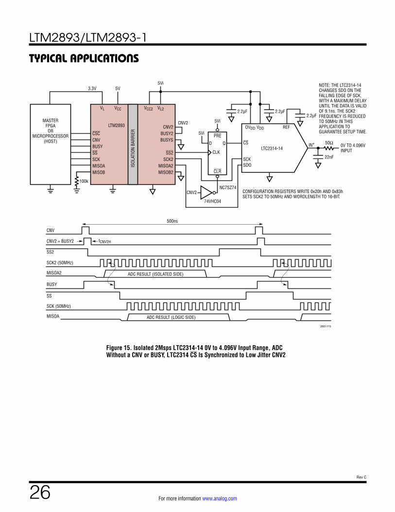
ADCs that do not have a conversion start or a busy signal are anticipated to allow reading of the prior SPI result while a conversion is ongoing. Connect the CNV2 signal to the BUSY2 signal. This will force the LTM2893 to read data from the ADC after the CNV2 signal goes low. This may include ADCs that use the CS signal to initiate a conver-sion start. An example of this is shown in Figure 15 with an LTC2314-14.
TIMING AND CONTROL
A conversion is initiated by CNV. A rising edge on CNV will start a conversion and start the process controlling the BUSY output and the collection of ADC results. Once a conversion has been initiated, do not start a new conver-sion until the current process is completed and the ADC results have been read or else data loss may occur. Once a CNV rising edge is detected, the BUSY output is asserted high and remains high throughout the ADC conversion phase and is de-asserted at the point the most significant bit is ready to be read. Reading data from the serial digital interface before the BUSY output is de-asserted will result in erroneous results and an assertion of the FAULT flag. To enable the serial digital interface assert the SS input low. The SS input allows the serial digital interface to be shared with other devices. When the device count is 1-2, the SS input may be held low at all times or asserted low at each read of the ADC results after the BUSY output has gone low. Asserting SS low at each ADC result read will allow a FAULT report to be cleared. At each SCK rising edge, the MISOA and MISOB data is read by the external master controller and the next data bit is registered to the MISOA and MISOB pin. The external master controller must read the result in one transaction prior to the next CNV rising edge.
LTM2893/LTM2893-1
13Rev C
For more information www.analog.com
APPLICATIONS INFORMATIONDIGITAL INTERFACE
The LTM2893 has a serial digital interface. The flexible VL supply allows the LTM2893 to communicate with digital logic operating between 1.71V and 5.5V, including 2.5V and 3.3V systems. The serial digital interface matches the characteristics of a serial peripheral interface bus (SPI) mode (0, 0) with a minor variation that data is captured on the rising edge and changes after the rising edge for SCK2 frequencies of 100MHz and 66MHz, except for MOSI2 on the LTM2893-1, which changes data on the falling edge of SCK2 in all cases. This variation allows for additional propagation and setup time to the next rising clock (SCK) edge, and should be transparent in most ap-plications. For SCK2 frequencies of 50MHz or less, data is captured on the rising edge of SCK and changes on the falling edge of SCK.
The serial output data is clocked out on the MISO pin when SS is low and an external clock is applied to the SCK pin. Clocking out the data immediately after the BUSY signal goes low will yield the best performance. When SS is high, the MISOA and MISOB pins are high impedance.
The serial digital interface is monitored by the fault detec-tion system watchdog for conditions that are considered a stalled process. Input timing is monitored for delays longer than tWATCHDOG_TIMEOUT between the rising edges of adjacent SCKs. The SCKs are counted and if the expected number is exceeded, the FAULT output will go low.
The rise and fall time of the logic signals into and out of the serial digital interface are approximately 1ns or less. Careful routing between the master device and the LTM2893 are necessary to avoid reflections resulting in incorrect data sampling or double clocking. Short direct routing with ground shielding is necessary. Avoid adding stubs to the signal routing as these may cause reflections.
STARTUP
The LTM2893 has an internal startup communication rou-tine to verify both sides of the isolation barrier are ready for communication. The startup routine is initiated when voltage is supplied to VCC and VCC2 inputs above 2.75V, VL and VL2 inputs above 1.5V, the logic side ON signal is high, and the Isolated ON2 signal is high. The BUSY signal will
go high and then low indicating the two internal isolators have completed the communication startup routine. Once the BUSY output goes low, the system is ready.
The isolated ON2 pin can be controlled by an external volt-age supervisor to delay the system ready signal until all isolated supplies and systems are ready. An example of this is demonstrated in Figure 16 with a LTC2917 configurable voltage supervisor. The logic side BUSY signal will stay high until the isolated side supervisor has verified the supplies are above the specified voltage.
BUSY INDICATOR (LOGIC SIDE)
The BUSY output pin goes high under three conditions: at startup, during data conversion, and when a watchdog timeout occurs. During normal operation, after a CNV rising edge, a high on the BUSY output indicates the ADC is currently converting an ADC result and is de-asserted when the data is ready to be read from MISOA and MISOB. Wait for the BUSY output to go low and wait a tSSFSCK delay before initiating the first SCK after SS is set low. This delay allows the most significant bit to be setup properly.
During startup the BUSY output is set high to indicate the LTM2893 is powering up and will be de-asserted when isolated communication is verified.
If a watchdog time-out occurs the BUSY signal will go high and the FAULT pin will go low.
BUSY2 AND BUSYS INPUTS (ISOLATED SIDE)
The isolated side signals BUSY2 and BUSYS control when the LTM2893 reads data from the ADC(s). Multiple con-figurations of the two isolated busy signals exist. Internally, the BUSY2 and the BUSYS input are logically OR-ed into a single busy response for which the falling edge is used to trigger the ready to read isolated SPI port function.
If a single ADC is connected to the LTM2893, the ADC BUSY output connects to the BUSY2 signal and BUSYS is connected to GND2, see Figure 14. Once the BUSY2 signal goes high then low, a SPI transaction will begin.
ADCs that contain a sleep function when two conversion start events are triggered without a SPI read must be treated differently. The LTM2893 does not wake up ADCs
LTM2893/LTM2893-1
14Rev C
For more information www.analog.com
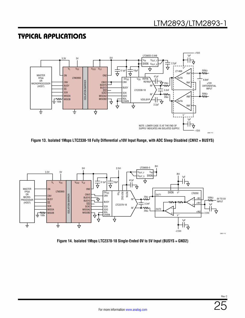
APPLICATIONS INFORMATIONthat use this function, such as the LTC2338 and LTC2328. In order to defeat this, connect the BUSYS signal to CNV2, and the ADCs’ BUSY signal to BUSY2. This will always keep the ADC awake, see Figure 13.
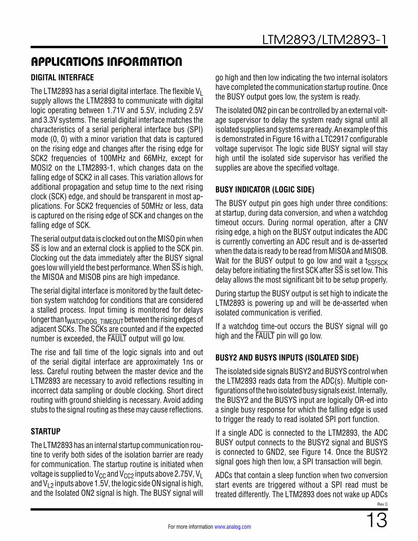
If the sleep function is needed, a select signal (SA, SB, or SC) can be used with 74VHC02 logic gates to disable this keep-alive function shown in Figure 2.
Table 1. Fault ReportingFAULTS CAUSE/TROUBLESHOOTING
Idle time during serial digital interface read during configuration write (CSC) or LTM2893-1
SCK↑ to SCK↑ > tWATCHDOG_TIMEOUT or SS or CSC↓ to SCK↑ > tWATCHDOG_TIMEOUT. Minimize delay between this relationship to less than tWATCHDOG_TIMEOUT. SCK frequency must be greater than the minimum referenced in Table 5.
Exceeding configured SCKs within a cycle
Exceeding the configured WORDLENGTH number of SCKs during a read is considered a fault.
Data loss in isolation communication
Common mode transients (GND to GND2) greater than 50kV/µs. High transient EM field disturbances greater than specified in EN61000, or an ESD event
Isolated side power loss
ON2, VL2, or VCC2 was removed and returned. Indicates unexpected interface loss.
CNV rising edge during serial digital interface read
Avoid transitioning CNV during the read of the serial digital interface. CNV will be ignored during the read of the serial digital interface.
SELECT SIGNALS
The select signal inputs SA, SB, and SC are communicated to the isolated side and output on SA2, SB2, and SC2 re-spectively. The select signals allow control of an external device related to the acquisition of an analog input signal. Select signals are communicated through the isolator on edge events. A static condition at start up is not com-municated to the isolated side. A transition is required to exit the default low output. Examples of device types anticipated for use on these pins are analog multiplexers (Figure 18) or programmable gain amplifiers. The signals can be used as logic controls for resets or power down functions that are not expected to occur during a conversion of an analog signal. The select signals are not designed for use as general purpose logic signals with asynchronous transition times relative to an analog to digital conversion. Use of these signals must be kept synchronous and outside of the operation of the CNV, BUSY, or SS active duration. Data and time sensitive information may be lost if a select signal transitions within 150ns of the CNV or SS signal.
Figure 2. ADC Keep-Alive and Sleep Enable
28931 F02
CNV2
BUSYS
LTM2893
BUSY2
74VHC02
ENABLE SLEEPSA2
32
1112
64
10
1
13
5
98
LTC2338-18
CNV
BUSY
IF ENABLE SLEEP = 0, BUSY SIGNALS PASSIF ENABLE SLEEP = 1, BUSY2,S = 0 ANDTWO CNV RISING EDGES WILL PUT ADC TO SLEEP
FAULT REPORTING
The FAULT pin indicates the occurrence of an internal communication error or an erroneous input condition. The FAULT pin is an open drain and requires an external pull up resistance for monitoring. If the FAULT pin is as-serted low, data loss may have occurred and the current transaction is suspected to contain an error. To clear the FAULT pin, return CNV low and SS high and initiate a new transaction with CNV or SS.
The LTM2893 does not have the provisions to provide the reason for the fault condition. Possible fault conditions are listed in Table 1. If the BUSY signal goes high and the FAULT pin goes low a watchdog time out has occurred. The configuration register is cleared and must be rewritten.
LTM2893/LTM2893-1
15Rev C
For more information www.analog.com
APPLICATIONS INFORMATIONThe direction of the SA, SB, or SC signals may be changed independently with the configuration register. The default condition of ‘0’ for each select bit maintains the signal flow from logic-to-isolated. Loading a ‘1’ into the direction bits will change the direction for that pin(s) to isolated-to-logic.
Warning: Careful planning is required for the use of SA, SB, and SC signals. Figure 12 shows the regions were transitions are safe and not safe for the logic side interface.
The select signals are sampled and transferred as a packet of the current value of the three signals. The select signal sampling will have up to 10ns of sampling jitter. If a signal transitions after another signal was sampled and is in the process of being transferred to the adjacent side, it will be delayed until the next available transmission slot. The delay may cause a perceived jitter or uncertainty of 80ns.
CONFIGURATION REGISTER
The LTM2893 contains a configuration register to adjust parameters of the speed and features of the ADC write and read process. After power up, write the configura-tion register by setting the CSC chip select input low and clocking in a one-byte configuration word with SCK and MOSI. The configuration register contains two bytes where the most significant bit of the SPI word selects which byte is addressed. Complete each configuration word by reasserting CSC high. The isolated side will be configured through an internal communication.
Table 3 shows the configuration register bit map for control-ling the operation and frequency of the logic and isolated interfaces. The configuration register allows adjustment of the default SCK frequency, direction of the SA, SB, SC to SA2, SB2, SC2 signals, the length of the SPI word and number of SPI words to process per SS cycle. Figure 8 demonstrates access to the configuration register.
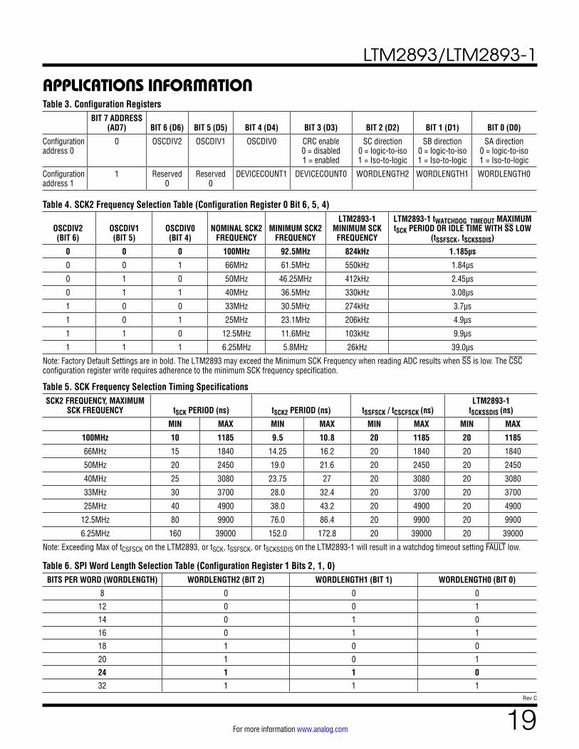
SCK AND SCK2 FREQUENCY
The SCK2 frequency selection list is shown in Table 4. Select the SCK2 frequency that is equal or less than the specifications of the ADC’s SPI port. Example: the LTC2338 has a 100MHz SCK maximum, 10ns minimum SCK period; therefore configure SCK2 for 100MHz.
The isolated SCK2 frequency is an internal trimmed oscil-lator. Graph SCK2 Frequency Variation versus Temperature shows the minimum and maximum characteristics over temperature and trim variation of the SCK2 frequency.
The logic-side SPI SCK frequency may be selected within a range that is dependent on the isolated-side’s SCK2 frequency. The minimum SCK frequency is limited to avoid triggering the watchdog timer and the maximum SCK frequency is limited to prevent a SPI buffer under-run.
To prevent a watchdog time out, the logic-side SPI SCK frequency must be at least 0.00795 times SCK2. If a watchdog timeout occurs, the FAULT flag will assert low.
To prevent a SPI buffer under-run, either the logic-side SPI SCK frequency must be less than the SCK2 frequency or there needs to be a sufficient delay after BUSY falls, tBUSYFSCKR, so that the buffer will be full enough to allow its reading at the desired logic-side SPI SCK frequency. If these conditions are not met and a buffer under-run occurs, then the FAULT flag will assert low.
Accounting for temperature and trim variations, the lowest SCK2 frequency will be 0.925 times the nominal SCK2 frequency.
The delay tBUSYFSCKR is calculated using Equation 1 and Table 2 lists values of tBUSYFSCKR for common operating conditions.
Equation 1:
tBUSYFSCKR ≥WORD COUNT • WORDLENGTH − 2
SCK2 • 0.925
−
+ 2ns, tSSFSCK,MIN
max
WORD COUNT • WORDLENGTH − 1SCKMAX
where tBUSYFSCKR is the time between the falling edge of BUSY and the 1st rising edge of SCK, SCK2 is the nominal configured frequency in Hz and SCK_MAX is the maximum frequency in Hz.
LTM2893/LTM2893-1
16Rev C
For more information www.analog.com
APPLICATIONS INFORMATIONNote that, provided the timing for SCK_MAX doesn’t vio-late the other SCK timing specifications, SCK_MAX may exceed SCK2 if the corresponding tBUSYFSCKR is observed.
Note that the minimum tSSFSCK of 20ns must also be independently satisfied and so, if the falling edge of SS is delayed sufficiently past the falling edge of BUSY, then the reading may need to be delayed beyond the value of tBUSYFSCKR calculated in Equation 1.
When the number of bits to be transferred (WORDCOUNT • WORDLENGTH) is equal to or less than 32 bits, the delay needed to meet timing at the maximum SCK frequency of 100MHz is equal to the minimum SS to SCK required and therefore no additional delay is required.
Table 2. BUSY Fall to SCK Rising Delay Required for Major Word Boundaries to Operate at Maximum SCK Under Worst Case SCK2 Tolerance
tBUSYFSCKR TOTAL NUMBER OF BITS PER SPI TRANSACTION
SCKMAX 32 64 96 128
100MHz 20ns 43ns 69ns 95ns
66MHz 24ns 64ns 103ns 142ns
50MHz 31ns 83ns 135ns 187ns
40MHz 38ns 103ns 168ns 233ns
33MHz 46ns 125ns 203ns 282ns
25MHz 60ns 164ns 267ns 371ns
12.5MHz 117ns 325ns 532ns 740ns
6.25MHz 232ns 647ns 1062ns 1477ns
CYCLIC REDUNDANCY CHECK (CRC)
The CRC enable selection bit (Config Register 0, bit 3) enables an internal CRC process to be completed during the communication of SPI data across the internal isolation barrier. The CRC is a 3-bit message added to the end of a SPI data word and is checked on the receiver side. The CRC is an internal function and the values are not readable. If the check fails, the FAULT pin is asserted low. When CRC is enabled, an additional wait of 225ns is required for the CRC to complete processing before the reassertion of a new SPI transaction or a new rising edge on CNV.
DEVICECOUNT AND WORDLENGTH
The DEVICECOUNT configuration bits select the number of words the LTM2893 will process. The selection of this value is based on the number of ADCs isolated or the number of words that must be written or read from the ADC. The DEVICECOUNT selection is used in conjunction with the WORDLENGTH selection bits. The WORDLENGTH is set to the number of bits per word. The WORDLENGTH selec-tion allows the SPI access to be tailored to a specific ADC result length to maximize throughput. When a controller that requires byte wide increments is used, set the word length to the number of bits on a byte size boundary (8, 16, 24, or 32). The total number of bits per SPI transac-tion is the WORD COUNT • WORDLENGTH as referenced in Table 6 and Table 7.
For example, a single 16-bit ADC is selected as DEVICE-COUNT of 1-2 with a WORDLENGTH of 16. Two 16 bit ADCs in parallel (SDO of ADC1 connected to MISOA2 and SDO of ADC2 connected to MISOB2) are also selected as a DEVICECOUNT of 1-2 with a word length of 16. Chaining a device increases the DEVICECOUNT. Chaining two ad-ditional ADCs through the first pair of ADCs would change the DEVICECOUNT to 3-4 with a word-length of 16.
The DEVICECOUNT is interchangeable with the number of words, WORD COUNT, a device requires for communica-tion. An example ADC may need 4 words of 32 bits. In this case, selecting the maximum DEVICECOUNT of 7-8 will write or read 4 words and setting the WORDLENGTH to 32 will set the length of each word. The LTM2893 writes or reads ½ the number of words as the DEVICECOUNT value. WORD COUNT is equal to ½ of DEVICECOUNT, see Table 7. A DEVICECOUNT of 1-2 will read 1 word, a DEVICECOUNT of 3-4 will read 2 words, a DEVICECOUNT of 5-6 will read 3 words, and a DEVICECOUNT of 7-8 will read 4 words.
LTM2893-1 ADC READ/WRITE
The LTM2893-1 writes a SPI word to the isolated ADC after the read operation. On the logic side, a SPI transac-tion will output data from MISOA, MISOB and read in a
LTM2893/LTM2893-1
17Rev C
For more information www.analog.com
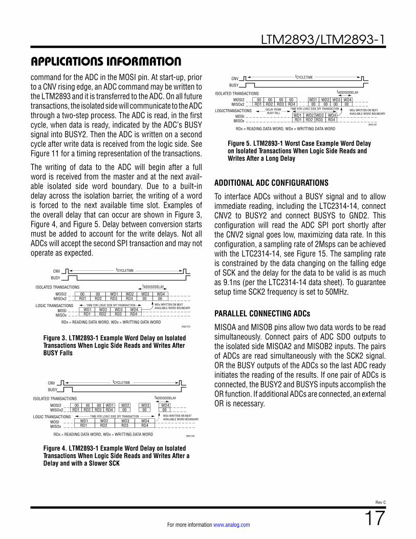
Figure 3. LTM2893-1 Example Word Delay on Isolated Transactions When Logic Side Reads and Writes After BUSY Falls
Figure 4. LTM2893-1 Example Word Delay on Isolated Transactions When Logic Side Reads and Writes After a Delay and with a Slower SCK
Figure 5. LTM2893-1 Worst Case Example Word Delay on Isolated Transactions When Logic Side Reads and Writes After a Long Delay
APPLICATIONS INFORMATIONcommand for the ADC in the MOSI pin. At start-up, prior to a CNV rising edge, an ADC command may be written to the LTM2893 and it is transferred to the ADC. On all future transactions, the isolated side will communicate to the ADC through a two-step process. The ADC is read, in the first cycle, when data is ready, indicated by the ADC’s BUSY signal into BUSY2. Then the ADC is written on a second cycle after write data is received from the logic side. See Figure 11 for a timing representation of the transactions.
The writing of data to the ADC will begin after a full word is received from the master and at the next avail-able isolated side word boundary. Due to a built-in delay across the isolation barrier, the writing of a word is forced to the next available time slot. Examples of the overall delay that can occur are shown in Figure 3, Figure 4, and Figure 5. Delay between conversion starts must be added to account for the write delays. Not all ADCs will accept the second SPI transaction and may not operate as expected.
ISOLATED TRANSACTIONS
LOGIC TRANSACTIONS
CNV
BUSY
MOSI2MISOx2
MOSIMISOx
RDx = READING DATA WORD, WDx = WRITTING DATA WORD2893 F03
00
tCYCLETIME
0000 00RD1
RD1 RD2
RD2 RD3 RD4
RD4RD3WD1 WD2 WD3 WD4
WD4WD3WD2WD1
WDx WRITTEN ON NEXT AVAILABLE WORD BOUNDARY
tADDISODELAY
TIME FOR LOGIC SIDE SPI TRANSACTION
CNV
BUSY
MOSI2MISOx2
MOSIMISOx
RDx = READING DATA WORD, WDx = WRITTING DATA WORD 2893 F04
00
tCYCLETIME
0000RD1
RD1 RD2
RD2 RD3 RD4
RD4RD3WD1 WD2 WD3 WD4
WD4WD3WD2WD1
WDx WRITTEN ON NEXT AVAILABLE WORD BOUNDARY
tADDISODELAY
000000
TIME FOR LOGIC SIDE SPI TRANSACTION
ISOLATED TRANSACTIONS
LOGIC TRANSACTIONS
CNV
BUSY
MOSI2MISOx2
MOSIMISOx
RDx = READING DATA WORD, WDx = WRITTING DATA WORD2893 F05
00
tCYCLETIME
0000RD1 RD2 RD3 RD4
WD4WD3WD2
WDx WRITTEN ON NEXTAVAILABLE WORD BOUNDARY
tADDISODELAY
000000
TIME FOR LOGIC SIDE SPI TRANSACTION
WD100
00
RD1WD1 WD2 WD3 WD4
RD2 RD3 RD4
DELAY FROM BUSY FALL
ISOLATED TRANSACTIONS
LOGICTRANSACTIONS
ADDITIONAL ADC CONFIGURATIONS
To interface ADCs without a BUSY signal and to allow immediate reading, including the LTC2314-14, connect CNV2 to BUSY2 and connect BUSYS to GND2. This configuration will read the ADC SPI port shortly after the CNV2 signal goes low, maximizing data rate. In this configuration, a sampling rate of 2Msps can be achieved with the LTC2314-14, see Figure 15. The sampling rate is constrained by the data changing on the falling edge of SCK and the delay for the data to be valid is as much as 9.1ns (per the LTC2314-14 data sheet). To guarantee setup time SCK2 frequency is set to 50MHz.
PARALLEL CONNECTING ADCs
MISOA and MISOB pins allow two data words to be read simultaneously. Connect pairs of ADC SDO outputs to the isolated side MISOA2 and MISOB2 inputs. The pairs of ADCs are read simultaneously with the SCK2 signal. OR the BUSY outputs of the ADCs so the last ADC ready initiates the reading of the results. If one pair of ADCs is connected, the BUSY2 and BUSYS inputs accomplish the OR function. If additional ADCs are connected, an external OR is necessary.
LTM2893/LTM2893-1
18Rev C
For more information www.analog.com
APPLICATIONS INFORMATION
28931 F07
LTM2893
SCK2
MISOA2
MISOB2
LTC2328-18
SCKSDOSDI CHAIN
LTC2328-18
SCKSDOSDI CHAIN
LTC2328-18
SCKSDOSDI CHAIN
LTC2328-18
SCKSDOSDI CHAIN
LTC2328-18
SCKSDOSDI CHAIN
LTC2328-18
SCKSDOSDI CHAIN
LTC2328-18
DEVICE 1 DEVICE 3 DEVICE 5 DEVICE 7
DEVICE 2 DEVICE 4 DEVICE 6 DEVICE 8
WORD COUNT =1 WORD COUNT =2 WORD COUNT =3 WORD COUNT =4
SCKSDOSDI CHAIN
LTC2328-18
SCKSDOSDI CHAIN
SET CONFIGURATION REGISTER OF LTM2893 SCK2DEVICECOUNT = 7-8 OR WORD COUNT = 4CONFIGURATION REGISTER COMMANDS0x10h, 0x9Eh (66MHz, 24-BITS) or 0x10h, 0x94h (66MHz, 18-BITS)
Figure 7. DEVICECOUNT, WORDCOUNT in Parallel and Chain Configuration
28931 F06
CNV2
BUSYS
LTM2893
BUSY2
SCK2
MISOA2
MISOB2
LTC2328-18
CNVSCKSDOSDIBUSY CHAIN
LTC2328-18
BUSYCNVSCKSDOSDI
SET CONFIGURATION REGISTER OF LTM2893 SCK2FREQUENCY 66MHz, DEVICECOUNT = 3-4 ORWORD COUNT = 2, WORDLENGTH = 18 OR 24.
CHAIN
LTC2328-18
CNVSCKSDOSDIBUSY CHAIN
LTC2328-18
BUSYCNVSCKSDOSDI
CHAIN
Figure 6. Connecting Four ADCs, One Chain Into MISOA2 and One Chain Into MISOB2
LTM2893/LTM2893-1
19Rev C
For more information www.analog.com
Table 3. Configuration RegistersBIT 7 ADDRESS
(AD7) BIT 6 (D6) BIT 5 (D5) BIT 4 (D4) BIT 3 (D3) BIT 2 (D2) BIT 1 (D1) BIT 0 (D0)
Configuration address 0
0 OSCDIV2 OSCDIV1 OSCDIV0 CRC enable 0 = disabled 1 = enabled
SC direction 0 = logic-to-iso 1 = Iso-to-logic
SB direction 0 = logic-to-iso 1 = Iso-to-logic
SA direction 0 = logic-to-iso 1 = Iso-to-logic
Configuration address 1
1 Reserved 0
Reserved 0
DEVICECOUNT1 DEVICECOUNT0 WORDLENGTH2 WORDLENGTH1 WORDLENGTH0
Table 4. SCK2 Frequency Selection Table (Configuration Register 0 Bit 6, 5, 4)
OSCDIV2 (BIT 6)
OSCDIV1 (BIT 5)
OSCDIV0 (BIT 4)
NOMINAL SCK2 FREQUENCY
MINIMUM SCK2 FREQUENCY
LTM2893-1 MINIMUM SCK FREQUENCY
LTM2893-1 tWATCHDOG_TIMEOUT MAXIMUM tSCK PERIOD OR IDLE TIME WITH SS LOW
(tSSFSCK, tSCKSSDIS)
0 0 0 100MHz 92.5MHz 824kHz 1.185µs
0 0 1 66MHz 61.5MHz 550kHz 1.84µs
0 1 0 50MHz 46.25MHz 412kHz 2.45µs
0 1 1 40MHz 36.5MHz 330kHz 3.08µs
1 0 0 33MHz 30.5MHz 274kHz 3.7µs
1 0 1 25MHz 23.1MHz 206kHz 4.9µs
1 1 0 12.5MHz 11.6MHz 103kHz 9.9µs
1 1 1 6.25MHz 5.8MHz 26kHz 39.0µs
Note: Factory Default Settings are in bold. The LTM2893 may exceed the Minimum SCK Frequency when reading ADC results when SS is low. The CSC configuration register write requires adherence to the minimum SCK frequency specification.
APPLICATIONS INFORMATION
Table 5. SCK Frequency Selection Timing SpecificationsSCK2 FREQUENCY, MAXIMUM
SCK FREQUENCY tSCK PERIOD (ns) tSCK2 PERIOD (ns) tSSFSCK / tCSCFSCK (ns)LTM2893-1
tSCKSSDIS (ns)
MIN MAX MIN MAX MIN MAX MIN MAX
100MHz 10 1185 9.5 10.8 20 1185 20 1185
66MHz 15 1840 14.25 16.2 20 1840 20 1840
50MHz 20 2450 19.0 21.6 20 2450 20 2450
40MHz 25 3080 23.75 27 20 3080 20 3080
33MHz 30 3700 28.0 32.4 20 3700 20 3700
25MHz 40 4900 38.0 43.2 20 4900 20 4900
12.5MHz 80 9900 76.0 86.4 20 9900 20 9900
6.25MHz 160 39000 152.0 172.8 20 39000 20 39000
Note: Exceeding Max of tCSFSCK on the LTM2893, or tSCK, tSSFSCK, or tSCKSSDIS on the LTM2893-1 will result in a watchdog timeout setting FAULT low.
Table 6. SPI Word Length Selection Table (Configuration Register 1 Bits 2, 1, 0)BITS PER WORD (WORDLENGTH) WORDLENGTH2 (BIT 2) WORDLENGTH1 (BIT 1) WORDLENGTH0 (BIT 0)
8 0 0 0
12 0 0 1
14 0 1 0
16 0 1 1
18 1 0 0
20 1 0 1
24 1 1 032 1 1 1
LTM2893/LTM2893-1
20Rev C
For more information www.analog.com
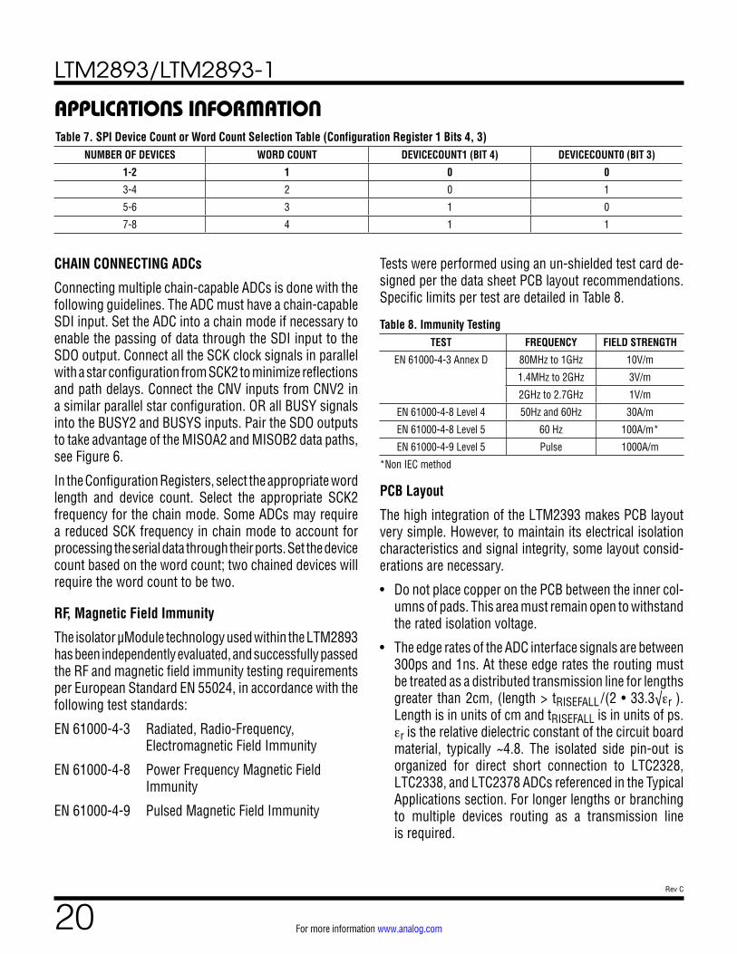
CHAIN CONNECTING ADCs
Connecting multiple chain-capable ADCs is done with the following guidelines. The ADC must have a chain-capable SDI input. Set the ADC into a chain mode if necessary to enable the passing of data through the SDI input to the SDO output. Connect all the SCK clock signals in parallel with a star configuration from SCK2 to minimize reflections and path delays. Connect the CNV inputs from CNV2 in a similar parallel star configuration. OR all BUSY signals into the BUSY2 and BUSYS inputs. Pair the SDO outputs to take advantage of the MISOA2 and MISOB2 data paths, see Figure 6.
In the Configuration Registers, select the appropriate word length and device count. Select the appropriate SCK2 frequency for the chain mode. Some ADCs may require a reduced SCK frequency in chain mode to account for processing the serial data through their ports. Set the device count based on the word count; two chained devices will require the word count to be two.
RF, Magnetic Field Immunity
The isolator µModule technology used within the LTM2893 has been independently evaluated, and successfully passed the RF and magnetic field immunity testing requirements per European Standard EN 55024, in accordance with the following test standards:
EN 61000-4-3 Radiated, Radio-Frequency, Electromagnetic Field Immunity
EN 61000-4-8 Power Frequency Magnetic Field Immunity
EN 61000-4-9 Pulsed Magnetic Field Immunity
APPLICATIONS INFORMATION
Tests were performed using an un-shielded test card de-signed per the data sheet PCB layout recommendations. Specific limits per test are detailed in Table 8.
Table 8. Immunity TestingTEST FREQUENCY FIELD STRENGTH
EN 61000-4-3 Annex D 80MHz to 1GHz 10V/m
1.4MHz to 2GHz 3V/m
2GHz to 2.7GHz 1V/m
EN 61000-4-8 Level 4 50Hz and 60Hz 30A/m
EN 61000-4-8 Level 5 60 Hz 100A/m*
EN 61000-4-9 Level 5 Pulse 1000A/m
*Non IEC method
PCB Layout
The high integration of the LTM2393 makes PCB layout very simple. However, to maintain its electrical isolation characteristics and signal integrity, some layout consid-erations are necessary.
• Do not place copper on the PCB between the inner col-umns of pads. This area must remain open to withstand the rated isolation voltage.
• The edge rates of the ADC interface signals are between 300ps and 1ns. At these edge rates the routing must be treated as a distributed transmission line for lengths greater than 2cm, (length > tRISEFALL /(2 • 33.3√εr ). Length is in units of cm and tRISEFALL is in units of ps. εr is the relative dielectric constant of the circuit board material, typically ~4.8. The isolated side pin-out is organized for direct short connection to LTC2328, LTC2338, and LTC2378 ADCs referenced in the Typical Applications section. For longer lengths or branching to multiple devices routing as a transmission line is required.
Table 7. SPI Device Count or Word Count Selection Table (Configuration Register 1 Bits 4, 3)NUMBER OF DEVICES WORD COUNT DEVICECOUNT1 (BIT 4) DEVICECOUNT0 (BIT 3)
1-2 1 0 0
3-4 2 0 1
5-6 3 1 0
7-8 4 1 1
LTM2893/LTM2893-1
21Rev C
For more information www.analog.com
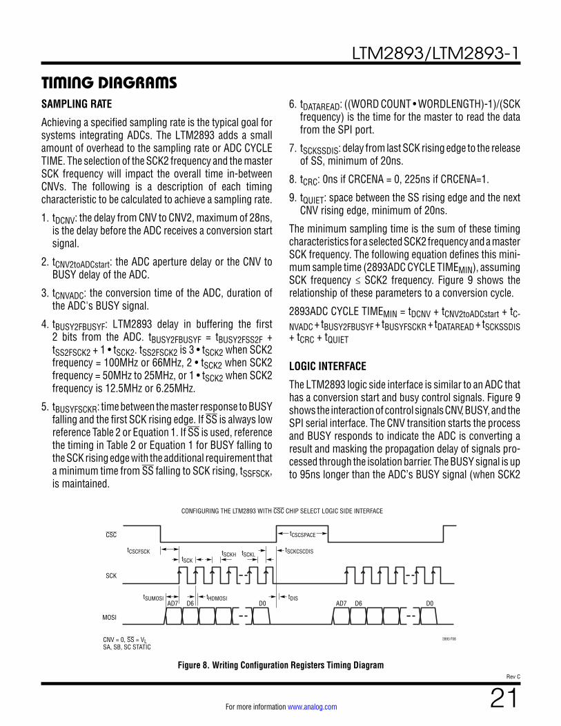
TIMING DIAGRAMSSAMPLING RATE
Achieving a specified sampling rate is the typical goal for systems integrating ADCs. The LTM2893 adds a small amount of overhead to the sampling rate or ADC CYCLE TIME. The selection of the SCK2 frequency and the master SCK frequency will impact the overall time in-between CNVs. The following is a description of each timing characteristic to be calculated to achieve a sampling rate.
1. tDCNV: the delay from CNV to CNV2, maximum of 28ns, is the delay before the ADC receives a conversion start signal.
2. tCNV2toADCstart: the ADC aperture delay or the CNV to BUSY delay of the ADC.
3. tCNVADC: the conversion time of the ADC, duration of the ADC's BUSY signal.
4. tBUSY2FBUSYF: LTM2893 delay in buffering the first 2 bits from the ADC. tBUSY2FBUSYF = tBUSY2FSS2F + tSS2FSCK2 + 1 • tSCK2. tSS2FSCK2 is 3 • tSCK2 when SCK2 frequency = 100MHz or 66MHz, 2 • tSCK2 when SCK2 frequency = 50MHz to 25MHz, or 1 • tSCK2 when SCK2 frequency is 12.5MHz or 6.25MHz.
5. tBUSYFSCKR: time between the master response to BUSY falling and the first SCK rising edge. If SS is always low reference Table 2 or Equation 1. If SS is used, reference the timing in Table 2 or Equation 1 for BUSY falling to the SCK rising edge with the additional requirement that a minimum time from SS falling to SCK rising, tSSFSCK, is maintained.
6. tDATAREAD: ((WORD COUNT • WORDLENGTH)-1)/(SCK frequency) is the time for the master to read the data from the SPI port.
7. tSCKSSDIS: delay from last SCK rising edge to the release of SS, minimum of 20ns.
8. tCRC: 0ns if CRCENA = 0, 225ns if CRCENA=1.
9. tQUIET: space between the SS rising edge and the next CNV rising edge, minimum of 20ns.
The minimum sampling time is the sum of these timing characteristics for a selected SCK2 frequency and a master SCK frequency. The following equation defines this mini-mum sample time (2893ADC CYCLE TIMEMIN), assuming SCK frequency ≤ SCK2 frequency. Figure 9 shows the relationship of these parameters to a conversion cycle.
2893ADC CYCLE TIMEMIN = tDCNV + tCNV2toADCstart + tC-NVADC + tBUSY2FBUSYF + tBUSYFSCKR + tDATAREAD + tSCKSSDIS + tCRC + tQUIET
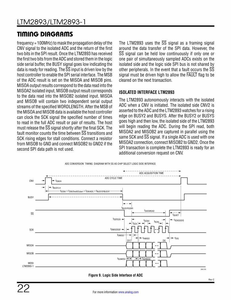
LOGIC INTERFACE
The LTM2893 logic side interface is similar to an ADC that has a conversion start and busy control signals. Figure 9 shows the interaction of control signals CNV, BUSY, and the SPI serial interface. The CNV transition starts the process and BUSY responds to indicate the ADC is converting a result and masking the propagation delay of signals pro-cessed through the isolation barrier. The BUSY signal is up to 95ns longer than the ADC’s BUSY signal (when SCK2
Figure 8. Writing Configuration Registers Timing Diagram
CONFIGURING THE LTM2893 WITH CSC CHIP SELECT LOGIC SIDE INTERFACE
CSC
SCK
MOSI
AD7 D0
tSCKtSCKH tSCKL
tCSCFSCK
AD7 D0D6 D6
CNV = 0, SS = VL SA, SB, SC STATIC
2893 F08
tSCKCSCDIS
tCSCSPACE
tDIStHDMOSItSUMOSI
LTM2893/LTM2893-1
22Rev C
For more information www.analog.com
TIMING DIAGRAMS
Figure 9. Logic Side Interface of ADC
frequency = 100MHz) to mask the propagation delay of the CNV signal to the isolated ADC and the return of the first two bits in the SPI result. Once the LTM2893 has received the first two bits from the ADC and stored them in the logic side serial buffer, the BUSY signal goes low indicating the data is ready for reading. The SS input is driven low by the host controller to enable the SPI serial interface. The MSB of the ADC result is set on the MISOA and MISOB pins. MISOA output results correspond to the data read into the MISOA2 isolated input, MISOB output result corresponds to the data read into the MISOB2 isolated input. MISOA and MISOB will contain two independent serial output streams of the specified WORDLENGTH. After the MSB of the MISOA and MISOB data is available the host controller can clock the SCK signal the specified number of times to read in the full ADC result or pair of results. The host must release the SS signal shortly after the final SCK. The fault monitor counts the time between SS transitions and SCK rising edges for stall conditions. Connect a resistor from MISOB to GND and connect MISOB2 to GND2 if the second SPI data path is not used.
The LTM2893 uses the SS signal as a framing signal around the data transfer of the SPI data. However, the SS signal can be held low continuously if only one or one pair of simultaneously sampled ADCs exists on the isolated side and the logic side SPI bus is not shared by other peripherals. In the event that a fault occurs the SS signal must be driven high to allow the FAULT flag to be cleared on the next transaction.
ISOLATED INTERFACE LTM2893
The LTM2893 autonomously interacts with the isolated ADC when a CNV is initiated. The isolated side CNV2 is asserted to the ADC and the LTM2893 watches for a rising edge on BUSY2 and BUSYS. After the BUSY2 or BUSYS goes high and then low, the isolated side of the LTM2893 will begin reading the ADC. During the SPI read, both MISOA2 and MISOB2 are captured in parallel using the same SCK and SS signal. If a single ADC is used with one MISOA2 connection, connect MISOB2 to GND2. Once the SPI transaction is complete the LTM2893 is ready for an additional conversion request on CNV.
CNV
BUSY
ADC CONVERSION TIMING DIAGRAM WITH SS AS CHIP SELECT LOGIC SIDE INTERFACE
SS
SCK
MISOA
D17
tDCNV + tCNV2toADCstart + tCNVADC + tBUSY2FBUSYF
tBUSYLH
D0
ADC CYCLE TIME
ADC ACQUISITION TIME
tQUIET
tDATAREAD
tSCKSSDIS
MISOB
MOSILTM2893-1
tBUSYFSCKR
tHDMOSI
2893 F09
tSUMOSI
tCNVH
tSSFSCK
tDMISOSSF
tDMISOtHMISO
tSCKLtSCKH
tSCK
tDIS
LTM2893/LTM2893-1
23Rev C
For more information www.analog.com
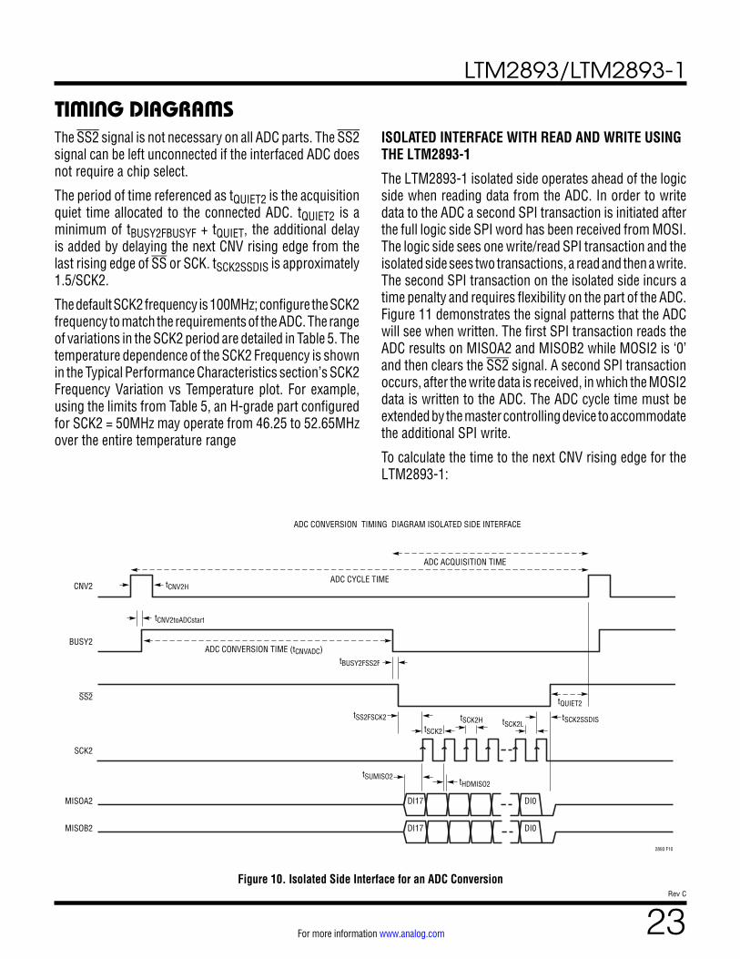
TIMING DIAGRAMSThe SS2 signal is not necessary on all ADC parts. The SS2 signal can be left unconnected if the interfaced ADC does not require a chip select.
The period of time referenced as tQUIET2 is the acquisition quiet time allocated to the connected ADC. tQUIET2 is a minimum of tBUSY2FBUSYF + tQUIET, the additional delay is added by delaying the next CNV rising edge from the last rising edge of SS or SCK. tSCK2SSDIS is approximately 1.5/SCK2.
The default SCK2 frequency is 100MHz; configure the SCK2 frequency to match the requirements of the ADC. The range of variations in the SCK2 period are detailed in Table 5. The temperature dependence of the SCK2 Frequency is shown in the Typical Performance Characteristics section’s SCK2 Frequency Variation vs Temperature plot. For example, using the limits from Table 5, an H-grade part configured for SCK2 = 50MHz may operate from 46.25 to 52.65MHz over the entire temperature range
ISOLATED INTERFACE WITH READ AND WRITE USING THE LTM2893-1
The LTM2893-1 isolated side operates ahead of the logic side when reading data from the ADC. In order to write data to the ADC a second SPI transaction is initiated after the full logic side SPI word has been received from MOSI. The logic side sees one write/read SPI transaction and the isolated side sees two transactions, a read and then a write. The second SPI transaction on the isolated side incurs a time penalty and requires flexibility on the part of the ADC. Figure 11 demonstrates the signal patterns that the ADC will see when written. The first SPI transaction reads the ADC results on MISOA2 and MISOB2 while MOSI2 is ‘0’ and then clears the SS2 signal. A second SPI transaction occurs, after the write data is received, in which the MOSI2 data is written to the ADC. The ADC cycle time must be extended by the master controlling device to accommodate the additional SPI write.
To calculate the time to the next CNV rising edge for the LTM2893-1:
Figure 10. Isolated Side Interface for an ADC Conversion
CNV2
BUSY2
ADC CONVERSION TIMING DIAGRAM ISOLATED SIDE INTERFACE
SS2
SCK2
MISOA2 DI17
ADC CONVERSION TIME (tCNVADC)
DI0
ADC CYCLE TIME
ADC ACQUISITION TIME
DI17 DI0MISOB2
2893 F10
tCNV2H
tCNV2toADCstart
tBUSY2FSS2F
tSS2FSCK2
tSCK2
tSCK2H tSCK2LtSCK2SSDIS
tQUIET2
tHDMISO2tSUMISO2
LTM2893/LTM2893-1
24Rev C
For more information www.analog.com
TIMING DIAGRAMS
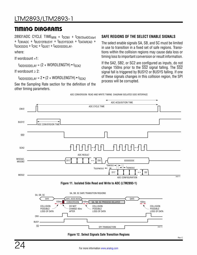
Figure 11. Isolated Side Read and Write to ADC (LTM2893-1)
28931ADC CYCLE TIMEMIN = tDCNV + tCNV2toADCstart + tCNVADC + tBUSY2FBUSYF + tBUSYFSCKR + tDATAREAD + tSCKSSDIS + tCRC + tQUIET + tADDISODELAY.
where:
If wordcount =1:
tADDISODELAY = (2 + WORDLENGTH) • tSCK2
If wordcount ≥ 2:
tADDISODELAY = 2 • (2 + WORDLENGTH) • tSCK2
See the Sampling Rate section for the definition of the other timing parameters.
SAFE REGIONS OF THE SELECT ENABLE SIGNALS
The select enable signals SA, SB, and SC must be limited in use to transition in a fixed set of safe regions. Transi-tions within the collision regions may cause data loss or timing loss to important conversion or result information.
If the SA2, SB2, or SC2 are configured as inputs, do not change 150ns prior to the SS2 signal falling. The SS2 signal fall is triggered by BUSY2 or BUSYS falling. If one of these signals changes in this collision region, the SPI process will be corrupted.
CNV2
BUSY2
ADC CONVERSION READ AND WRITE TIMING DIAGRAM ISOLATED SIDE INTERFACE
SS2
SCK2
MISOA2,MISOB2 DI17
ADC CONVERSION TIME
DI0
ADC CYCLE TIME
ADC ACQUISITION TIME
MOSI2D17 D0
ADC RESULT
ADC CONFIGURATION
tDMOSI2tHDMOSI2tSS2FMOSI2
XXXXXXXX
2893 F11
Figure 12. Select Signals Safe Transition Regions
SA, SB, SC SAFE TRANSITION REGIONS
SAFE SAFE150ns
CNV
COLLISION POSSIBLE LOSS OF DATA
SPI TRANSACTION
DO NOT CHANGE 40ns AFTER
CONVERSION SA, SB, SC PROCESS DELAYED
COLLISION POSSIBLE LOSS OF DATA
150ns150ns
SA, SB, SC
BUSY
SS
SAFE, ADDS NOISE
2893 F12
COLLISION POSSIBLE LOSS OF DATA
LTM2893/LTM2893-1
25Rev C
For more information www.analog.com
TYPICAL APPLICATIONS
Figure 13. Isolated 1Msps LTC2338-18 Fully Differential ±10V Input Range, with ADC Sleep Disabled (CNV2 = BUSYS)
LTM2893
100k
VL VCC VL2VCC2
CNVBUSYSSSCKMISOAMISOB
ON ON2
CNV2BUSYSBUSY2
SS2
CNV
RDLCHAIN
VDD
5Vi5V3.3V
REFINOVDDREFBUF
VDDLBYP
IN+
IN–
VIN
SHDN
VOUT_F
VOUT_S
0.1µF 10µF
2.2µF
47µF
3.3nF
INA+
V+
V–
INA–
OUTA
2.2µF
LTC2338-18
LTC6655-2.048
LT1469
20Ω6.8nF
±10VDIFFERENTIAL
INPUT
500Ω
INB+
INB–
OUTA
NOTE: LOWER CASE i’S AT THE END OFSUPPLY INDICATES AN ISOLATED SUPPLY.
500Ω
MASTERFPGAOR
MICROPROCESSOR(HOST)
28931 F13
1µF
1µF
+15Vi
–15Vi
ISOL
ATIO
N BA
RRIE
RBUSY
SCKSDO
SCK2MISOA2MISOB2
20Ω
LTM2893
100k
VL VCC VL2VCC2
CNVBUSYSSSCKMISOAMISOB
ON ON2
CNV2BUSYSBUSY2
SS2
CNV
RDLCHAIN
VDD
5Vi 2.5Vi
5V3.3V
REFIN
OVDD
REF/DGC IN+
IN–
VIN
SHDN
VOUT_F
VOUT_S
0.1µF 10µF47µF
3.3nF
20ΩOUT1
OUT2
V+SHDN
V–
LTC2378-18
LT6350
LTC6655-5
0V TO 5VINPUT
500Ω
MASTERFPGAOR
MICRO-PROCESSOR
(HOST)
28931 F13
1µF
1µF
8Vi
–2.5Vi
ISOL
ATIO
N BA
RRIE
R
BUSY
SCKSDO
SCK2MISOA2MISOB2
+–
+–
8Vi
–IN1
+IN1
+IN2 2.5Vi
1µF
20Ω
Figure 14. Isolated 1Msps LTC2378-18 Single-Ended 0V to 5V Input (BUSYS = GND2)
LTM2893/LTM2893-1
26Rev C
For more information www.analog.com
TYPICAL APPLICATIONS
Figure 15. Isolated 2Msps LTC2314-14 0V to 4.096V Input Range, ADC Without a CNV or BUSY, LTC2314 CS Is Synchronized to Low Jitter CNV2
LTM2893
100k
VL VCC VL2VCC2
CSCCNVBUSYSSSCKMISOAMISOB
CNV2BUSY2BUSYS
SS2SCK2
MISOA2MISOB2
VDD
5Vi5V3.3V
REFOVDD
IN+
2.2µF 2.2µF2.2µF
LTC2314-14
CNV2
5Vi
5Vi
CONFIGURATION REGISTERS WRITE 0x20h AND 0x83hSETS SCK2 TO 50MHz AND WORDLENGTH TO 16-BIT.
NOTE: THE LTC2314-14 CHANGES SDO ON THE FALLING EDGE OF SCK, WITH A MAXIMUM DELAY UNTIL THE DATA IS VALID OF 9.1ns. THE SCK2 FREQUENCY IS REDUCED TO 50MHz IN THIS APPLICATION TO GUARANTEE SETUP TIME.
MASTERFPGAOR
MICROPROCESSOR(HOST)
28931 F15
ISOL
ATIO
N BA
RRIE
R
SCKSDO
22nF
50Ω 0V TO 4.096VINPUT
BUSY
CNV
CNV2 = BUSY2
SS2
SCK2 (50MHz)
tCNV2H
MISOA2 ADC RESULT (ISOLATED SIDE)
SS
SCK (50MHz)
MISOA ADC RESULT (LOGIC SIDE)
500ns
CSPRE
CLR
D
CLK
NC7SZ74
CNV2
74VHC04
Q
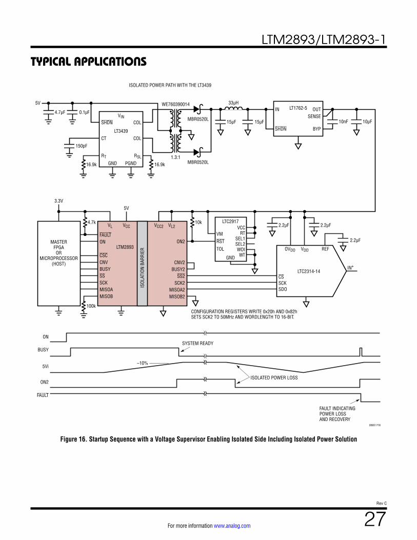
LTM2893/LTM2893-1
27Rev C
For more information www.analog.com
TYPICAL APPLICATIONS
Figure 16. Startup Sequence with a Voltage Supervisor Enabling Isolated Side Including Isolated Power Solution
LTM2893
VL VCC VL2VCC2
FAULTON
CSCCNVBUSYSSSCKMISOAMISOB
CNV2BUSY2
SS2SCK2
MISOA2MISOB2
ON2VDD
5V3.3V
4.7k
REFOVDD
IN+
2.2µF 2.2µF
2.2µF
LTC2314-14
CONFIGURATION REGISTERS WRITE 0x20h AND 0x82hSETS SCK2 TO 50MHz AND WORDLENGTH TO 16-BIT.
MASTERFPGAOR
MICROPROCESSOR(HOST)
28931 F16
ISOL
ATIO
N BA
RRIE
R
CSSCKSDO
10k
VM
RST
TOL
VCCRT
SEL1SEL2WDIWT
LTC2917
GND
LT3439
VIN
GND PGND
SHDN
CT
RT
COL
COL
RSL
16.9k
150pF
16.9k
0.1µF4.7µF
5V WE760390014
1.3:1
ISOLATED POWER PATH WITH THE LT3439
MBR0520L
MBR0520L
33µH
15µF 15µF 10nFSHDN
IN OUTSENSE
BYP
LT1762-5
10µF
ON
BUSY
ON2
5Vi
FAULT
–10%
FAULT INDICATING POWER LOSSAND RECOVERY
SYSTEM READY
ISOLATED POWER LOSS
100k
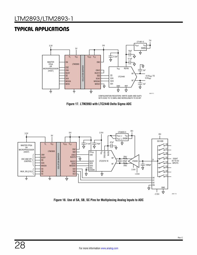
LTM2893/LTM2893-1
28Rev C
For more information www.analog.com
TYPICAL APPLICATIONS
Figure 17. LTM2893 with LTC2440 Delta Sigma ADC
Figure 18. Use of SA, SB, SC Pins for Multiplexing Analog Inputs to ADC
LTM2893
VL VCC VL2VCC2
CSCCNVBUSYSSSCKMISOAMOSI
CNV2BUSY2
SS2SCK2
MISOA2MOSI2
ON ON2
VCC
CSSCKSDOSDI
5Vi
5V3.3V
REFIN
GND REF
IN+
IN–
VIN
SHDN
VOUT
2.2µF0.1µF
10µF
1µF
1µF
LTC2440
LT1461-5
MASTERFPGAOR
MICROPROCESSOR(HOST)
28931 F17
ISOL
ATIO
N BA
RRIE
R
7Vi
–0.5VREF TO0.5VREF
CONFIGURATION REGISTERS: WRITE 0x60h AND 0x87hSETS SCK2 TO 12.5MHz AND WORDLENGTH TO 32-BIT
LTM2893
VL VCC VL2VCC2
CNVBUSYSSSCKMISOA
ON2
CNV2BUSYS
SS2
SA2SB2SC2
SASBSC
CNV
CNV AND SPICONTROL
MUX_SEL[2:0]
RDLCHAIN
VDD
5Vi 2.5Vi
5V3.3V
REFIN
OVDD
REF/DGC
IN+
IN–
VIN
SHDN
VOUT_F
VOUT_S
0.1µF 10µF47µF
20Ω
20Ω
330pFLTC2378-18
LTC6655-5
MASTER FPGAOR
MICROPROCESSOR(HOST)
28931 F18
ISOL
ATIO
N BA
RRIE
R
BUSYSCKSDO
BUSY2SCK2
MISOA2
8Vi
8Vi
2.5Vi
–2.5Vi
LT6350
GND
–2.5Vi
DG1408
EIGHT0V TO 5VINPUTS
1000pF
D
S8
S7
S6
S5
S4
S3
S2
S1A0A1A2EN
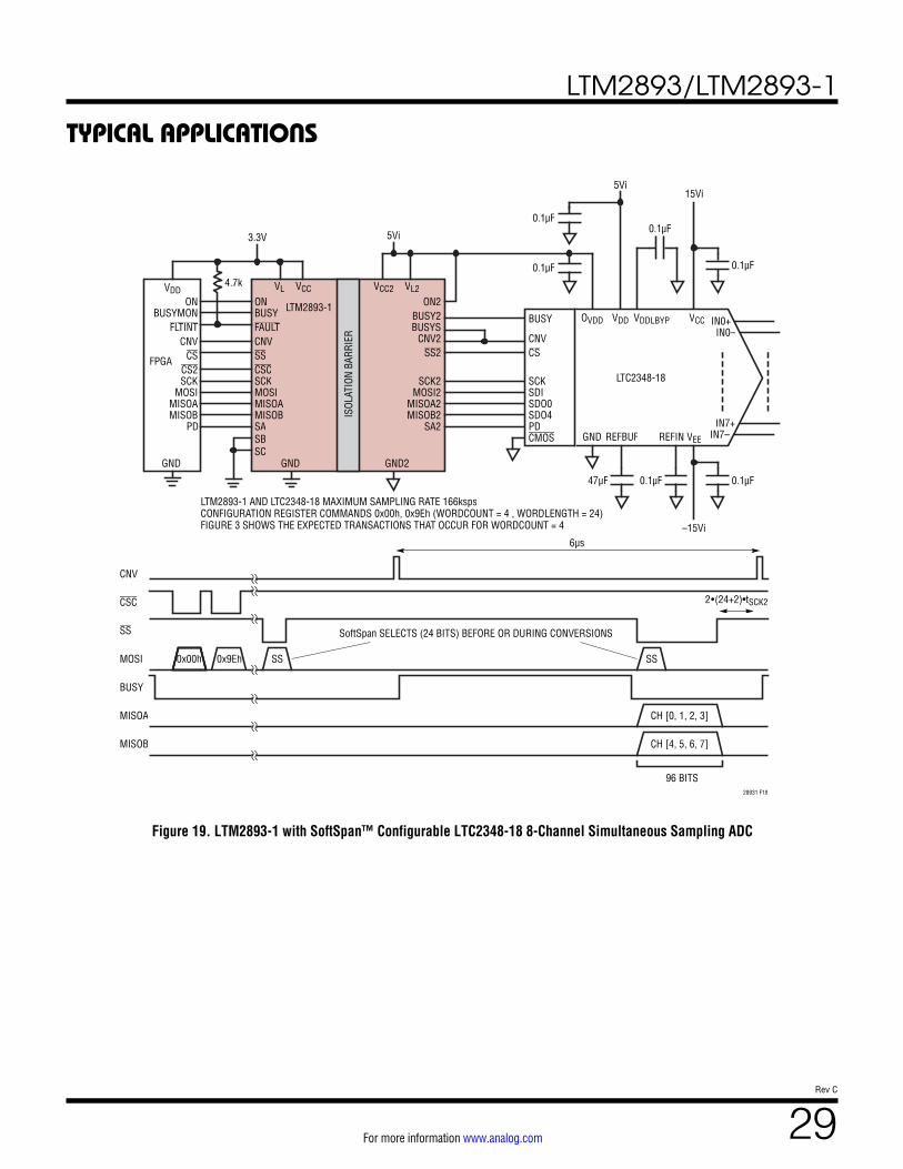
LTM2893/LTM2893-1
29Rev C
For more information www.analog.com
TYPICAL APPLICATIONS
Figure 19. LTM2893-1 with SoftSpan™ Configurable LTC2348-18 8-Channel Simultaneous Sampling ADC
4.7k
0.1µF
0.1µF
0.1µF47µF 0.1µF
0.1µF
0.1µF
VL2VCC2ON2
CNV2SS2
SCK2MOSI2
MISOA2
SA2
GND2
VL VCCON
CSCSCKMOSIMISOA
SASBSC
GND
CNV
BUSYFAULT
SSIS
OLAT
ION
BARR
IER
ON
PD
CS2SCK
MOSI
CNV
BUSYMONFLTINT
CS
MISOA
VDD
GND
5Vi3.3V
LTM2893-1
FPGA
BUSY2BUSYS
MISOB2MISOB
IN0+IN0–
VDD
5Vi
REFINGND
CS
SDO0
SCK
BUSY
CNV
LTC2348-18
OVDD
SDI
SDO4PDCMOS
IN7+IN7–REFBUF VEE
–15Vi
VCC
15Vi
VDDLBYP
MISOB
LTM2893-1 AND LTC2348-18 MAXIMUM SAMPLING RATE 166kspsCONFIGURATION REGISTER COMMANDS 0x00h, 0x9Eh (WORDCOUNT = 4 , WORDLENGTH = 24)FIGURE 3 SHOWS THE EXPECTED TRANSACTIONS THAT OCCUR FOR WORDCOUNT = 4
CSC
SS
MOSI 0x00h 0x9Eh SS
CNV
6µs
BUSY
MISOA
MISOB
CH [0, 1, 2, 3]
CH [4, 5, 6, 7]
96 BITS
SS
SoftSpan SELECTS (24 BITS) BEFORE OR DURING CONVERSIONS
2•(24+2)•tSCK2
28931 F19

LTM2893/LTM2893-1
30Rev C
For more information www.analog.com
PACKAGE DESCRIPTIONBGA Package
36-Lead (15mm × 6.25mm × 2.06mm)(Reference LTC DWG # 05-08-1987 Rev Ø)
PACKAGE TOP VIEW
4
PIN “A1”CORNER
YX
aaa Z
aaa Z
BGA Package36-Lead (15mm × 6.25mm × 2.06mm)(Reference LTC DWG# 05-08-1987 Rev Ø)
NOTES:1. DIMENSIONING AND TOLERANCING PER ASME Y14.5M-1994
2. ALL DIMENSIONS ARE IN MILLIMETERS
BALL DESIGNATION PER JESD MS-028 AND JEP95
4
3
DETAILS OF PIN #1 IDENTIFIER ARE OPTIONAL,BUT MUST BE LOCATED WITHIN THE ZONE INDICATED.THE PIN #1 IDENTIFIER MAY BE EITHER A MOLD OR MARKED FEATURE
DETAIL A
Øb (36 PLACES)
DETAIL B
SUBSTRATE
A
A1
b1
ccc Z
DETAIL BPACKAGE SIDE VIEW
MOLDCAP
Z
M X YZdddM Zeee
SYMBOLA
A1A2b
b1DEeFG
H1H2aaabbbcccdddeee
MIN1.860.401.460.450.47
0.510.95
NOM2.060.501.560.600.50
15.006.251.00
13.755.000.561.00
MAX2.260.601.660.750.53
0.611.050.150.100.150.150.08
NOTES
DIMENSIONS
TOTAL NUMBER OF BALLS: 36
A2
D
E
SUGGESTED PCB LAYOUTTOP VIEW
0.00
5.875
6.875
4.875
1.50
1.50
0.50
2.50
2.50
0.50
0.00
6.875
5.875
4.875
6.675
6.125
// b
bb Z Z
H2H1
5. PRIMARY DATUM -Z- IS SEATING PLANE
6. SOLDER BALL COMPOSITION IS 96.5% Sn/3.0% Ag/0.5% Cu
0.50 ±0.025 Ø 36x
2.75
2.25
BGA 36 0914 REV Ø
TRAY PIN 1BEVEL
PACKAGE IN TRAY LOADING ORIENTATION
COMPONENTPIN “A1”
LTMXXXXXXµModule
7 PACKAGE ROW AND COLUMN LABELING MAY VARY AMONG µModule PRODUCTS. REVIEW EACH PACKAGE LAYOUT CAREFULLY
!
PACKAGE BOTTOM VIEW
R
P
N
M
L
K
J
H
G
F
E
D
C
B
A
123456
DETAIL A
3
SEE NOTESPIN 1
e
e
F
Gb
7
SEE NOTES
b
LTM2893/LTM2893-1
31Rev C
For more information www.analog.com
REVISION HISTORYREV DATE DESCRIPTION PAGE NUMBER
A 03/17 Corrected VCC2 pin number on Block DiagramCorrected SCK and tBUSYFSCKR formulasCorrection to Table 2. BUSY Fall to SCK Rising Delay Required for Major Word Boundaries to Operate at Maximum SCK Under Worst Case SCK2 ToleranceCorrection to Table 4. SCK2 Frequency SelectionMultiple corrections to Table 5. SCK Frequency Selection Timing SpecificationsCorrections to multiple sampling rate parameters (tBUSY2FBUSYF, tBUSYFSCKR, tDATAREAD)
101516
191921
B 05/17 Revised SS pin descriptionRevised SCK2 frequency range calculation for H-gradeRevised tADC_CYCLE_TIME_MIN equation
82324
C 02/18 Added UL/CSA Certifications 1, 5
Information furnished by Analog Devices is believed to be accurate and reliable. However, no responsibility is assumed by Analog Devices for its use, nor for any infringements of patents or other rights of third parties that may result from its use. Specifications subject to change without notice. No license is granted by implication or otherwise under any patent or patent rights of Analog Devices.
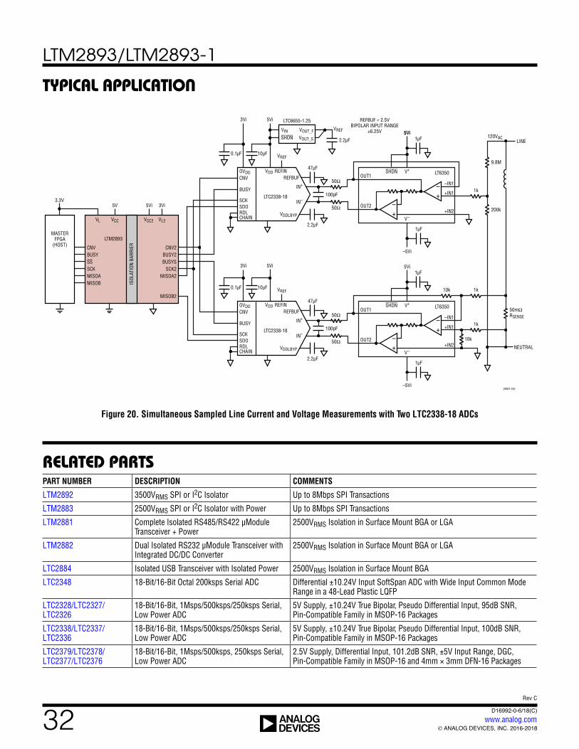
LTM2893/LTM2893-1
32Rev C
For more information www.analog.com
D16992-0-6/18(C)www.analog.com
ANALOG DEVICES, INC. 2016-2018
RELATED PARTS
TYPICAL APPLICATION
PART NUMBER DESCRIPTION COMMENTS
LTM2892 3500VRMS SPI or I2C Isolator Up to 8Mbps SPI Transactions
LTM2883 2500VRMS SPI or I2C Isolator with Power Up to 8Mbps SPI Transactions
LTM2881 Complete Isolated RS485/RS422 µModule Transceiver + Power
2500VRMS Isolation in Surface Mount BGA or LGA
LTM2882 Dual Isolated RS232 µModule Transceiver with Integrated DC/DC Converter
2500VRMS Isolation in Surface Mount BGA or LGA
LTC2884 Isolated USB Transceiver with Isolated Power 2500VRMS Isolation in Surface Mount BGA
LTC2348 18-Bit/16-Bit Octal 200ksps Serial ADC Differential ±10.24V Input SoftSpan ADC with Wide Input Common Mode Range in a 48-Lead Plastic LQFP
LTC2328/LTC2327/LTC2326
18-Bit/16-Bit, 1Msps/500ksps/250ksps Serial, Low Power ADC
5V Supply, ±10.24V True Bipolar, Pseudo Differential Input, 95dB SNR, Pin-Compatible Family in MSOP-16 Packages
LTC2338/LTC2337/LTC2336
18-Bit/16-Bit, 1Msps/500ksps/250ksps Serial, Low Power ADC
5V Supply, ±10.24V True Bipolar, Pseudo Differential Input, 100dB SNR, Pin-Compatible Family in MSOP-16 Packages
LTC2379/LTC2378/LTC2377/LTC2376
18-Bit/16-Bit, 1Msps/500ksps, 250ksps Serial, Low Power ADC
2.5V Supply, Differential Input, 101.2dB SNR, ±5V Input Range, DGC, Pin-Compatible Family in MSOP-16 and 4mm × 3mm DFN-16 Packages
Figure 20. Simultaneous Sampled Line Current and Voltage Measurements with Two LTC2338-18 ADCs
LTM2893
VL VCC VL2VCC2
CNVBUSYSSSCKMISOAMISOB
CNV2BUSY2BUSYS
SCK2MISOA2
MISOB2
CNV
RDLCHAIN
VDD
VREF
VREF
3Vi5Vi
5Vi3Vi
5V3.3V
REFINOVDDREFBUF
VDDLBYP
IN+
IN–
VIN
SHDN
VOUT_F
VOUT_S
0.1µF 10µF
47µF
50Ω
50Ω
2.2µF
100pF
2.2µF
OUT1
OUT2
V+SHDN
V–
LTC2338-18
LT6350
1k
200k
LTC6655-1.25
MASTERFPGA
(HOST)
28931 F20
1µF
1µF
5Vi
REFBUF = 2.5VBIPOLAR INPUT RANGE
±6.25V
–5Vi
ISOL
ATIO
N BA
RRIE
R
BUSY
SCKSDO
+–
+–
–IN1
+IN1
+IN2
CNV
RDLCHAIN
VDD
VREF
5Vi3Vi
REFINOVDDREFBUF
VDDLBYP
IN+
IN–
0.1µF 10µF
47µF
50Ω
50Ω
2.2µF
100pF
OUT1
OUT2
V+SHDN
V–
LTC2338-18
LT6350
1µF
1µF
5Vi
–5Vi
BUSY
SCKSDO
+–
+–
–IN1
+IN1
+IN2
9.8M
LINE
1k
1k
10k
10k
50mΩRSENSE
NEUTRAL
120VAC5Vi