
LTC4269-1 - IEEE 802.3at PD with Synchronous No-Opto ... · The LTC®4269-1 is an integrated...
44
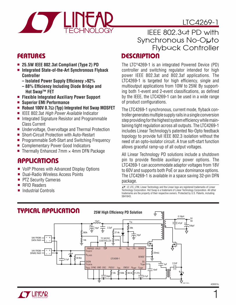
LTC4269-1 1 42691fc • • • • 33mΩ 39k 10μF 30.9Ω 1.21k 38.3k 100k 12k 10nF 10μF 2.2μF 0.1μF 33pF 0.1μF 2.2nF 1μF t ON SYNC PGDLY UVLO PWRGD SENSE – V CMP SENSE + R CMP V NEG SHDN R CLASS V PORTP V PORTN ENDLY OSC LTC4269-1 GND FB V CC V IN SG PG C CMP 10μH TO MICRO CONTROLLER • 47μF 0.18μH 5V 5A 100μF + + 3.01k 27.4k T2P 14k 383k 54V FROM DATA PAIR 54V FROM SPARE PAIR + – ~ ~ + – ~ ~ 42691 TA01a TYPICAL APPLICATION FEATURES APPLICATIONS DESCRIPTION IEEE 802.3at PD with Synchronous No-Opto Flyback Controller The LTC ® 4269-1 is an integrated Powered Device (PD) controller and switching regulator intended for high power IEEE 802.3at and 802.3af applications. The LTC4269-1 is targeted for high efficiency, single and multioutput applications from 10W to 25W. By support- ing both 1-event and 2-event classifications, as defined by the IEEE, the LTC4269-1 can be used in a wide range of product configurations. The LTC4269-1 synchronous, current mode, flyback con- troller generates multiple supply rails in a single conversion step providing for the highest system efficiency while main- taining tight regulation across all outputs. The LTC4269-1 includes Linear Technology’s patented No-Opto feedback topology to provide full IEEE 802.3 isolation without the need of an opto-isolator circuit. A true soft-start function allows graceful ramp-up of all output voltages. All Linear Technology PD solutions include a shutdown pin to provide flexible auxiliary power options. The LTC4269-1 can accommodate adaptor voltages from 18V to 60V and supports both PoE or aux dominance options. The LTC4269-1 is available in a space saving 32-pin DFN package. L, LT, LTC, LTM, Linear Technology and the Linear logo are registered trademarks of Linear Technology Corporation. Hot Swap is a trademark of Linear Technology Corporation. All other trademarks are the property of their respective owners. Protected by U.S. Patents, including 5841643. n 25.5W IEEE 802.3at Compliant (Type 2) PD n Integrated State-of-the-Art Synchronous Flyback Controller – Isolated Power Supply Efficiency >92% – 88% Efficiency Including Diode Bridge and Hot Swap™ FET n Flexible Integrated Auxiliary Power Support n Superior EMI Performance n Robust 100V 0.7Ω (Typ) Integrated Hot Swap MOSFET n IEEE 802.3at High Power Available Indicator n Integrated Signature Resistor and Programmable Class Current n Undervoltage, Overvoltage and Thermal Protection n Short-Circuit Protection with Auto-Restart n Programmable Soft-Start and Switching Frequency n Complementary Power Good Indicators n Thermally Enhanced 7mm × 4mm DFN Package n VoIP Phones with Advanced Display Options n Dual-Radio Wireless Access Points n PTZ Security Cameras n RFID Readers n Industrial Controls 25W High Efficiency PD Solution
-
Upload
nguyenhuong -
Category
Documents
-
view
222 -
download
0
Transcript of LTC4269-1 - IEEE 802.3at PD with Synchronous No-Opto ... · The LTC®4269-1 is an integrated...
LTC4269-1
142691fc
•
•
••
33mΩ
39k
10μF
30.9Ω
1.21k38.3k100k12k
10nF
10μF 2.2μF
0.1μF33pF
0.1μF
2.2nF1μF
tONSYNC PGDLY
UVLOPWRGD
SENSE–
VCMP
SENSE+
RCMPVNEG
SHDN
RCLASS
VPORTP
VPORTN
ENDLYOSC
LTC4269-1
GND
FB VCC
VIN
SG
PG
CCMP
10μH
TO MICROCONTROLLER
•
47μF
0.18μH5V5A
100μF++
3.01k
27.4k
T2P
14k
383k
54V FROMDATA PAIR
54V FROMSPARE PAIR
+–
~~
+–
~~
42691 TA01a
TYPICAL APPLICATION
FEATURES
APPLICATIONS
DESCRIPTION
IEEE 802.3at PD with Synchronous No-Opto
Flyback Controller
The LTC®4269-1 is an integrated Powered Device (PD) controller and switching regulator intended for high power IEEE 802.3at and 802.3af applications. The LTC4269-1 is targeted for high effi ciency, single and multioutput applications from 10W to 25W. By support-ing both 1-event and 2-event classifi cations, as defi ned by the IEEE, the LTC4269-1 can be used in a wide range of product confi gurations.
The LTC4269-1 synchronous, current mode, fl yback con-troller generates multiple supply rails in a single conversion step providing for the highest system effi ciency while main-taining tight regulation across all outputs. The LTC4269-1 includes Linear Technology’s patented No-Opto feedback topology to provide full IEEE 802.3 isolation without the need of an opto-isolator circuit. A true soft-start function allows graceful ramp-up of all output voltages.
All Linear Technology PD solutions include a shutdown pin to provide fl exible auxiliary power options. The LTC4269-1 can accommodate adaptor voltages from 18V to 60V and supports both PoE or aux dominance options. The LTC4269-1 is available in a space saving 32-pin DFN package.L, LT, LTC, LTM, Linear Technology and the Linear logo are registered trademarks of Linear Technology Corporation. Hot Swap is a trademark of Linear Technology Corporation. All other trademarks are the property of their respective owners. Protected by U.S. Patents, including 5841643.
n 25.5W IEEE 802.3at Compliant (Type 2) PDn Integrated State-of-the-Art Synchronous Flyback
Controller – Isolated Power Supply Effi ciency >92% – 88% Effi ciency Including Diode Bridge and
Hot Swap™ FETn Flexible Integrated Auxiliary Power Supportn Superior EMI Performancen Robust 100V 0.7Ω (Typ) Integrated Hot Swap MOSFETn IEEE 802.3at High Power Available Indicatorn Integrated Signature Resistor and Programmable
Class Currentn Undervoltage, Overvoltage and Thermal Protectionn Short-Circuit Protection with Auto-Restartn Programmable Soft-Start and Switching Frequencyn Complementary Power Good Indicatorsn Thermally Enhanced 7mm × 4mm DFN Package
n VoIP Phones with Advanced Display Optionsn Dual-Radio Wireless Access Pointsn PTZ Security Camerasn RFID Readersn Industrial Controls
25W High Effi ciency PD Solution
LTC4269-1
242691fc
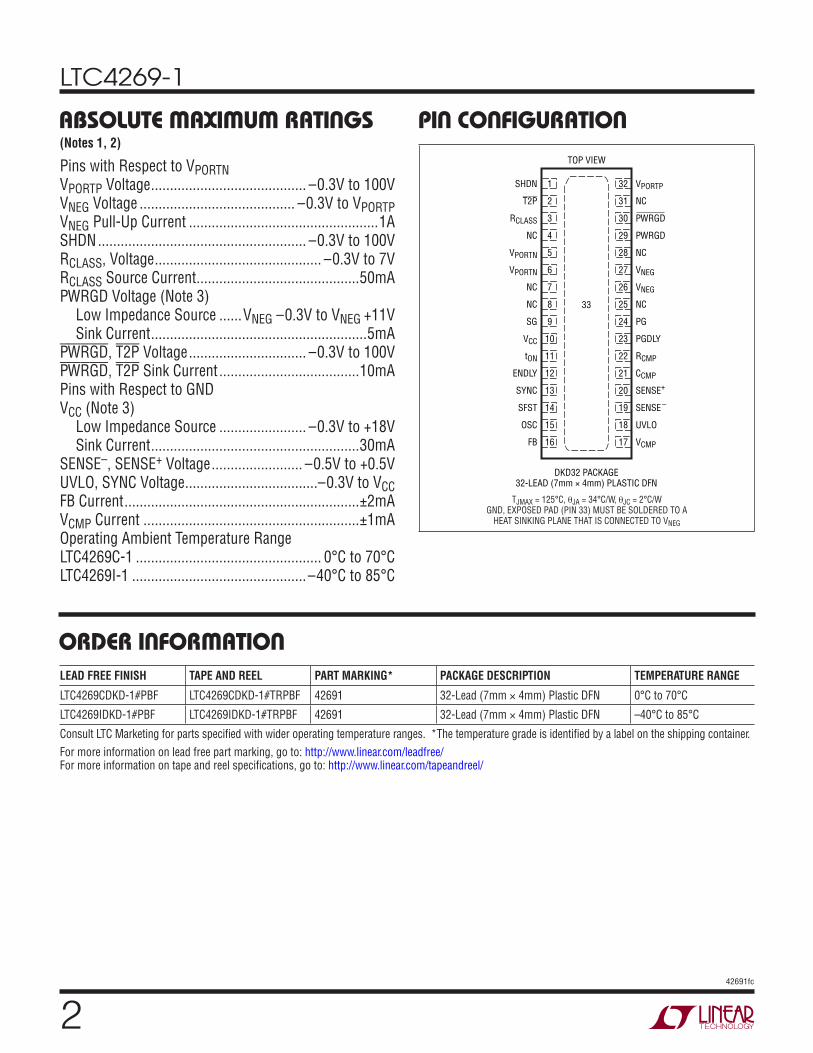
PIN CONFIGURATIONABSOLUTE MAXIMUM RATINGS
Pins with Respect to VPORTN VPORTP Voltage ......................................... –0.3V to 100VVNEG Voltage ......................................... –0.3V to VPORTP
VNEG Pull-Up Current ..................................................1ASHDN ....................................................... –0.3V to 100VRCLASS, Voltage ............................................ –0.3V to 7VRCLASS Source Current ...........................................50mAPWRGD Voltage (Note 3) Low Impedance Source ......VNEG –0.3V to VNEG +11V Sink Current .........................................................5mAPWRGD, T2P Voltage ............................... –0.3V to 100V PWRGD, T2P Sink Current .....................................10mAPins with Respect to GNDVCC (Note 3) Low Impedance Source ....................... –0.3V to +18V Sink Current .......................................................30mASENSE–, SENSE+ Voltage ........................ –0.5V to +0.5VUVLO, SYNC Voltage ...................................–0.3V to VCC FB Current ..............................................................±2mAVCMP Current .........................................................±1mAOperating Ambient Temperature RangeLTC4269C-1 ................................................. 0°C to 70°CLTC4269I-1 ..............................................–40°C to 85°C
(Notes 1, 2)
32
31
30
29
28
27
26
25
24
23
22
21
20
19
18
17
33
1
2
3
4
5
6
7
8
9
10
11
12
13
14
15
16
VPORTP
NC
PWRGD
PWRGD
NC
VNEG
VNEG
NC
PG
PGDLY
RCMP
CCMP
SENSE+
SENSE –
UVLO
VCMP
SHDN
T2P
RCLASS
NC
VPORTN
VPORTN
NC
NC
SG
VCC
tON
ENDLY
SYNC
SFST
OSC
FB
TOP VIEW
DKD32 PACKAGE32-LEAD (7mm × 4mm) PLASTIC DFN
TJMAX = 125°C, θJA = 34°C/W, θJC = 2°C/WGND, EXPOSED PAD (PIN 33) MUST BE SOLDERED TO A
HEAT SINKING PLANE THAT IS CONNECTED TO VNEG
ORDER INFORMATIONLEAD FREE FINISH TAPE AND REEL PART MARKING* PACKAGE DESCRIPTION TEMPERATURE RANGE
LTC4269CDKD-1#PBF LTC4269CDKD-1#TRPBF 42691 32-Lead (7mm × 4mm) Plastic DFN 0°C to 70°C
LTC4269IDKD-1#PBF LTC4269IDKD-1#TRPBF 42691 32-Lead (7mm × 4mm) Plastic DFN –40°C to 85°C
Consult LTC Marketing for parts specifi ed with wider operating temperature ranges. *The temperature grade is identifi ed by a label on the shipping container.
For more information on lead free part marking, go to: http://www.linear.com/leadfree/ For more information on tape and reel specifi cations, go to: http://www.linear.com/tapeandreel/
LTC4269-1
342691fc
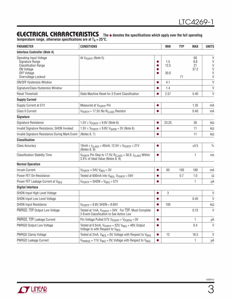
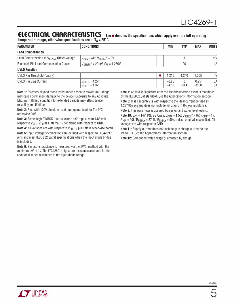
ELECTRICAL CHARACTERISTICS The l denotes the specifi cations which apply over the full operating temperature range, otherwise specifi cations are at TA = 25°C.
PARAMETER CONDITIONS MIN TYP MAX UNITS
Interface Controller (Note 4)
Operating Input VoltageSignature RangeClassifi cation RangeON VoltageOFF VoltageOvervoltage Lockout
At VPORTP (Note 5)l
l
l
l
1.512.5
30.071
609.821
37.2
VVVVV V
ON/OFF Hysteresis Window l 4.1 V
Signature/Class Hysteresis Window l 1.4 V
Reset Threshold State Machine Reset for 2-Event Classifi cation l 2.57 5.40 V
Supply Current
Supply Current at 57V Measured at VPORTP Pin l 1.35 mA
Class 0 Current VPORTP = 17.5V, No RCLASS Resistor l 0.40 mA
Signature
Signature Resistance 1.5V ≤ VPORTP ≤ 9.8V (Note 6) l 23.25 26 kΩ
Invalid Signature Resistance, SHDN Invoked 1.5V ≤ VPORTP ≤ 9.8V, VSHDN = 3V (Note 6) l 11 kΩ
Invalid Signature Resistance During Mark Event (Notes 6, 7) l 11 kΩ
Classifi cation
Class Accuracy 10mA < ICLASS < 40mA, 12.5V < VPORTP < 21V (Notes 8, 9)
l ±3.5 %
Classifi cation Stability Time VPORTP Pin Step to 17.5V, RCLASS = 30.9, ICLASS Within 3.5% of Ideal Value (Notes 8, 9)
l 1 ms
Normal Operation
Inrush Current VPORTP = 54V, VNEG = 3V l 60 100 180 mA
Power FET On-Resistance Tested at 600mA into VNEG, VPORTP = 54V l 0.7 1.0 Ω
Power FET Leakage Current at VNEG VPORTP = SHDN = VNEG = 57V l 1 μA
Digital Interface
SHDN Input High Level Voltage l 3 V
SHDN Input Low Level Voltage l 0.45 V
SHDN Input Resistance VPORTP = 9.8V, SHDN = 9.65V l 100 kΩ
PWRGD, T2P Output Low Voltage Tested at 1mA, VPORTP = 54V. For T2P, Must Complete 2-Event Classifi cation to See Active Low
l 0.15 V
PWRGD, T2P Leakage Current Pin Voltage Pulled 57V, VPORTP = VPORTN = 0V l 1 μA
PWRGD Output Low Voltage Tested at 0.5mA, VPORTP = 52V, VNEG = 48V, Output Voltage Is with Respect to VNEG
l 0.4 V
PWRGD Clamp Voltage Tested at 2mA, VNEG = 0V, Voltage with Respect to VNEG l 12 16.5 V
PWRGD Leakage Current VPWRGD = 11V, VNEG = 0V, Voltage with Respect to VNEG l 1 μA
LTC4269-1
442691fc
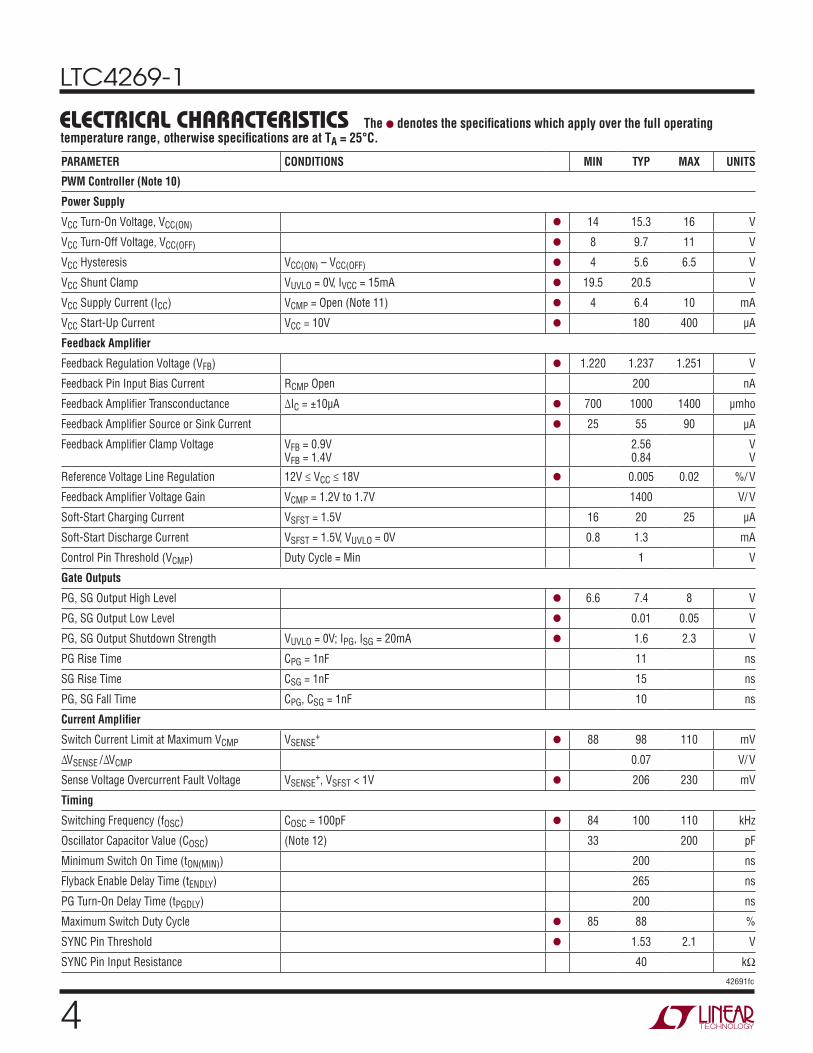
ELECTRICAL CHARACTERISTICS The l denotes the specifi cations which apply over the full operating temperature range, otherwise specifi cations are at TA = 25°C.
PARAMETER CONDITIONS MIN TYP MAX UNITS
PWM Controller (Note 10)
Power Supply
VCC Turn-On Voltage, VCC(ON) l 14 15.3 16 V
VCC Turn-Off Voltage, VCC(OFF) ● 8 9.7 11 V
VCC Hysteresis VCC(ON) – VCC(OFF) ● 4 5.6 6.5 V
VCC Shunt Clamp VUVLO = 0V, IVCC = 15mA ● 19.5 20.5 V
VCC Supply Current (ICC) VCMP = Open (Note 11) ● 4 6.4 10 mA
VCC Start-Up Current VCC = 10V ● 180 400 μA
Feedback Amplifi er
Feedback Regulation Voltage (VFB) ● 1.220 1.237 1.251 V
Feedback Pin Input Bias Current RCMP Open 200 nA
Feedback Amplifi er Transconductance ΔIC = ±10μA ● 700 1000 1400 μmho
Feedback Amplifi er Source or Sink Current ● 25 55 90 μA
Feedback Amplifi er Clamp Voltage VFB = 0.9VVFB = 1.4V
2.560.84
VV
Reference Voltage Line Regulation 12V ≤ VCC ≤ 18V ● 0.005 0.02 %/ V
Feedback Amplifi er Voltage Gain VCMP = 1.2V to 1.7V 1400 V/ V
Soft-Start Charging Current VSFST = 1.5V 16 20 25 μA
Soft-Start Discharge Current VSFST = 1.5V, VUVLO = 0V 0.8 1.3 mA
Control Pin Threshold (VCMP) Duty Cycle = Min 1 V
Gate Outputs
PG, SG Output High Level ● 6.6 7.4 8 V
PG, SG Output Low Level ● 0.01 0.05 V
PG, SG Output Shutdown Strength VUVLO = 0V; IPG, ISG = 20mA ● 1.6 2.3 V
PG Rise Time CPG = 1nF 11 ns
SG Rise Time CSG = 1nF 15 ns
PG, SG Fall Time CPG, CSG = 1nF 10 ns
Current Amplifi er
Switch Current Limit at Maximum VCMP VSENSE+ ● 88 98 110 mV
ΔVSENSE /ΔVCMP 0.07 V/ V
Sense Voltage Overcurrent Fault Voltage VSENSE+, VSFST < 1V ● 206 230 mV
Timing
Switching Frequency (fOSC) COSC = 100pF ● 84 100 110 kHz
Oscillator Capacitor Value (COSC) (Note 12) 33 200 pF
Minimum Switch On Time (tON(MIN)) 200 ns
Flyback Enable Delay Time (tENDLY) 265 ns
PG Turn-On Delay Time (tPGDLY) 200 ns
Maximum Switch Duty Cycle ● 85 88 %
SYNC Pin Threshold ● 1.53 2.1 V
SYNC Pin Input Resistance 40 kΩ
LTC4269-1
542691fc
Note 1: Stresses beyond those listed under Absolute Maximum Ratings
may cause permanent damage to the device. Exposure to any Absolute
Maximum Rating condition for extended periods may affect device
reliability and lifetime.
Note 2: Pins with 100V absolute maximum guaranteed for T ≥ 0°C,
otherwise 90V.
Note 3: Active high PWRGD internal clamp self-regulates to 14V with
respect to VNEG. VCC has internal 19.5V clamp with respect to GND.
Note 4: All voltages are with respect to VPORTN pin unless otherwise noted.
Note 5: Input voltage specifi cations are defi ned with respect to LTC4269-1
pins and meet IEEE 802.3af/at specifi cations when the input diode bridge
is included.
Note 6: Signature resistance is measured via the ΔV/ΔI method with the
minimum ΔV of 1V. The LTC4269-1 signature resistance accounts for the
additional series resistance in the input diode bridge.
Note 7: An invalid signature after the 1st classifi cation event is mandated
by the IEEE802.3at standard. See the Applications Information section.
Note 8: Class accuracy is with respect to the ideal current defi ned as
1.237/RCLASS and does not include variations in RCLASS resistance.
Note 9: This parameter is assured by design and wafer level testing.
Note 10: VCC = 14V; PG, SG Open; VCMP = 1.5V, VSENSE– = 0V, RCMP = 1k,
RtON = 90k, RPGDLY = 27.4k, RENDLY = 90k, unless otherwise specifi ed. All
voltages are with respect to GND.
Note 11: Supply current does not include gate charge current to the
MOSFETs. See the Applications Information section.
Note 12: Component value range guaranteed by design.
ELECTRICAL CHARACTERISTICS The l denotes the specifi cations which apply over the full operating temperature range, otherwise specifi cations are at TA = 25°C.
PARAMETER CONDITIONS MIN TYP MAX UNITS
Load Compensation
Load Compensation to VSENSE Offset Voltage VRCMP with VSENSE+ = 0V 1 mV
Feedback Pin Load Compensation Current VSENSE+ = 20mV, VFB = 1.230V 20 μA
UVLO Function
UVLO Pin Threshold (VUVLO) ● 1.215 1.240 1.265 V
UVLO Pin Bias Current VUVLO = 1.2VVUVLO = 1.3V
–0.25–4.50
0–3.4
0.25–2.50
μAμA
LTC4269-1
642691fc
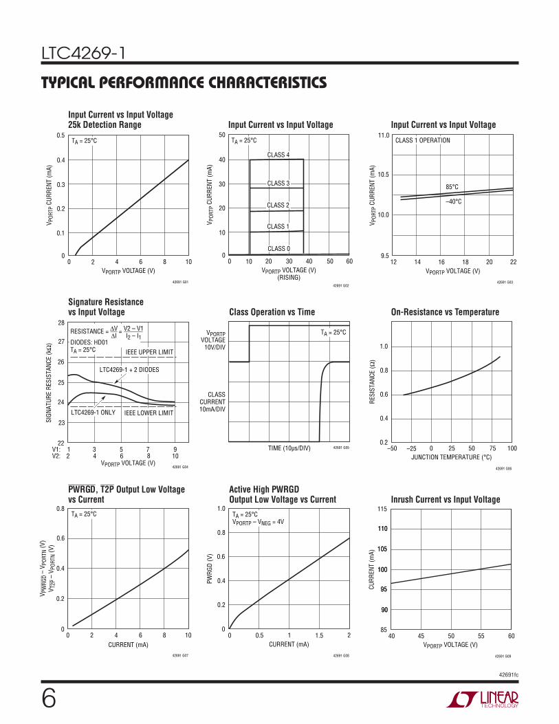
TYPICAL PERFORMANCE CHARACTERISTICS
Input Current vs Input Voltage 25k Detection Range Input Current vs Input Voltage Input Current vs Input Voltage
VPORTP VOLTAGE (V)
00
VP
OR
TP C
UR
REN
T (
mA
)
0.1
0.2
0.3
0.4
0.5
2 4 6 8
42691 G01
10
TA = 25°C
VPORTP VOLTAGE (V)(RISING)
00
VP
OR
TP C
UR
REN
T (
mA
)
10
20
30
40
50
10 20 30 40
42691 G02
50 60
TA = 25°C
CLASS 4
CLASS 3
CLASS 2
CLASS 1
CLASS 0
VPORTP VOLTAGE (V)
129.5
VP
OR
TP C
UR
REN
T (
mA
)
10.5
14 16
42691 G03
10.0
18 20 22
11.0
85°C
–40°C
CLASS 1 OPERATION
Signature Resistance vs Input Voltage
PWRGD, T2P Output Low Voltage vs Current
Active High PWRGD Output Low Voltage vs Current Inrush Current vs Input Voltage
CURRENT (mA)
0
VP
WR
GD
– V
PO
RTN
(V
)
VT2P –
VP
OR
TN
(V
)
0.4
0.6
8
42691 G07
0.2
02 4 6 10
0.8TA = 25°C
CURRENT (mA)
00
PW
RG
D (
V)
0.4
1.0
0.5 1
42691 G08
0.2
0.8
0.6
1.5 2
TA = 25°CVPORTP – VNEG = 4V
VPORTP VOLTAGE (V)
4085
CU
RR
EN
T (
mA
)
115
45 50
42691 G09
55 60
90
100
105
110
95
90
100
105
110
95
Class Operation vs Time On-Resistance vs Temperature
VPORTP VOLTAGE (V)
122
V1:V2:
SIG
NA
TU
RE R
ES
ISTA
NC
E (
kΩ)
23
25
26
27
3 5
42691 G04
24
7 96 102 4 8
28
RESISTANCE =
DIODES: HD01TA = 25°C
= VI
V2 – V1I2 – I1
IEEE UPPER LIMIT
IEEE LOWER LIMITLTC4269-1 ONLY
LTC4269-1 + 2 DIODES
VPORTPVOLTAGE
10V/DIV
CLASSCURRENT10mA/DIV
TIME (10μs/DIV) 42691 G05
TA = 25°C
JUNCTION TEMPERATURE (°C)
–500.2
RES
ISTA
NC
E (
Ω)
0.4
0.6
0.8
1.0
–25 0 25 50
42691 G06
75 100
LTC4269-1
742691fc
TEMPERATURE (°C)
–50
VC
C (
V)
15
25
42691 G10
12
10
–25 0 50
9
8
16
14
13
11
75 100 125
VCC(ON)
VCC(OFF)
TEMPERATURE (°C)
–50
I VC
C (
μA
)
200
250
300
25 75
42691 G11
150
100
–25 0 50 100 125
50
0
TEMPERATURE (°C)
–50
8
9
25 75
42691 G12
7
6
–25 0 50 100 125
5
4
3
10
I VC
C (
mA
)
DYNAMIC CURRENT CPG = 1nF,CSG = 1nF, fOSC = 100kHz
STATIC PART CURRENT
VCC = 14V
TEMPERATURE (°C)
–5090
SEN
SE V
OLTA
GE (
mV
)
92
96
98
100
110
104
0 50 75
42691 G13
94
106
108
102
–25 25 100 125
FB = 1.1VSENSE = VSENSE
+ WITH VSENSE
– = 0V
TEMPERATURE (°C)
–50
SEN
SE V
OLTA
GE (
mV
)
215
25
42691 G14
200
190
–25 0 50
185
180
220
210
205
195
75 100 125
SENSE = VSENSE+
WITH VSENSE– = 0V
TEMPERATURE (°C)
–5090
f OS
C (
kHz)
92
96
98
100
110
104
0 50 75
42691 G15
94
106
108
102
–25 25 100 125
COSC = 100pF
TEMPERATURE (°C)
–501.230
VFB
(V
)
1.231
1.233
1.234
1.235
1.240
1.237
0 50 75
42691 G16
1.232
1.238
1.239
1.236
–25 25 100 125
TEMPERATURE (°C)
–50
FEED
BA
CK
PIN
IN
PU
T B
IAS
(nA
)
200
250
300
25 75
42691 G17
150
100
–25 0 50 100 125
50
0
RCMP OPEN
TEMPERATURE (°C)
–50
VFB
RES
ET (
V)
1.03
25
42691 G18
1.00
0.98
–25 0 50
0.97
0.96
1.04
1.02
1.01
0.99
75 100 125
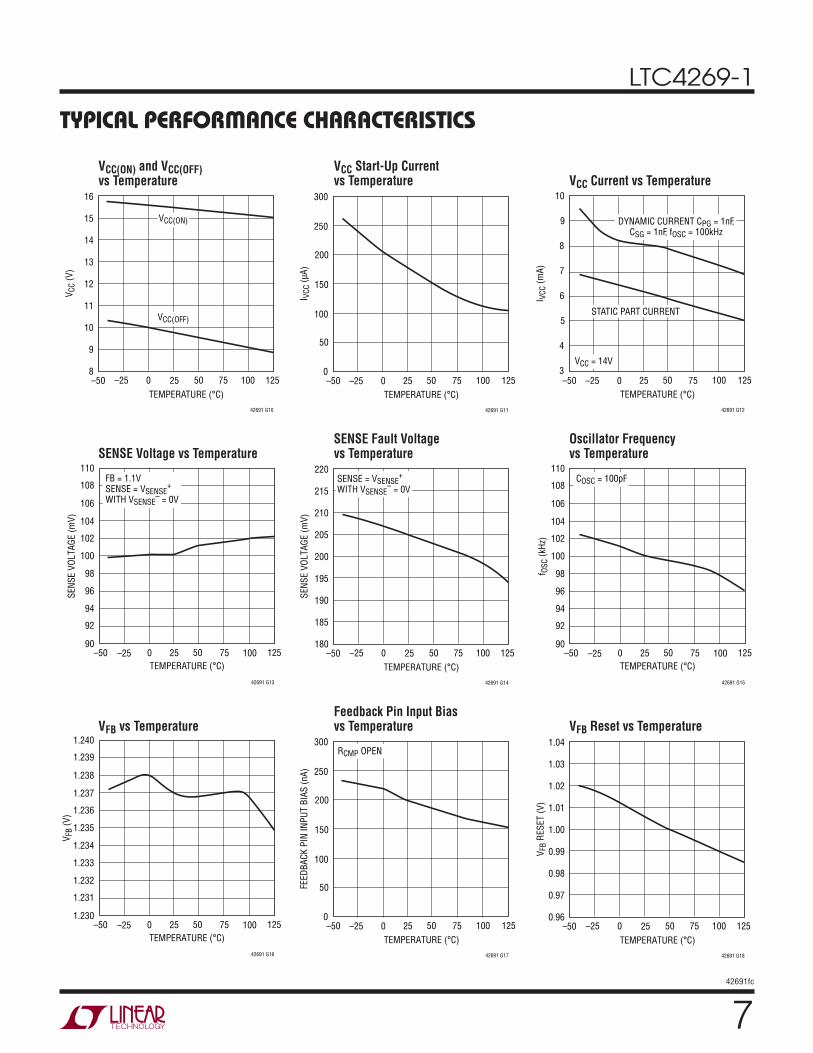
TYPICAL PERFORMANCE CHARACTERISTICS
VCC(ON) and VCC(OFF) vs Temperature
VCC Start-Up Current vs Temperature VCC Current vs Temperature
SENSE Voltage vs TemperatureSENSE Fault Voltage vs Temperature
Oscillator Frequency vs Temperature
VFB vs TemperatureFeedback Pin Input Bias vs Temperature VFB Reset vs Temperature
LTC4269-1
842691fc
VFB (V)
0.9–70
I VC
MP (
μA
)
–50
–30
–10
70
30
1 1.1 1.4
50
10
1.2 1.3 1.5
42691 G19
125°C
25°C
–40°C
TEMPERATURE (°C)
–50
I VC
MP (
μA
)
60
65
70
25 75
42691 G20
55
50
–25 0 50 100 125
45
40
SOURCE CURRENTVFB = 1.1V
SINKCURRENTVFB = 1.4V
TEMPERATURE (°C)
–50900
gm
(μm
ho)
950
1000
1050
1100
–25 0 25 50
42691 G21
75 100 125
TEMPERATURE (°C)
–50
AV (
V/V
)
1550
25
42691 G22
1400
1300
–25 0 50
1250
1200
1150
1100
1600
1650
1700
1500
1450
1350
75 100 125
TEMPERATURE (°C)
–50
UV
LO
(V
)
1.240
1.245
1.250
25 75
42691 G23
1.235
1.230
–25 0 50 100 125
1.225
1.220
TEMPERATURE (°C)
–50
3.4
3.5
3.7
25 75
42691 G24
3.3
3.2
–25 0 50 100 125
3.1
3.0
3.6
I UV
LO
(μA
)
TEMPERATURE (°C)
–50
SFS
T C
HA
RG
E C
UR
REN
T (
μA
)
23
25
42691 G25
20
18
–25 0 50
17
16
15
22
21
19
75 100 125
CAPACITANCE (nF)
0
TIM
E (
ns)
80
70
60
50
40
30
20
10
08
42691 G26
2 4 6 1071 3 5 9
TA = 25°C
FALL TIME
RISE TIME
TEMPERATURE (°C)
–50 –2519.0
VC
C (
V)
20.0
21.5
0 50 75
42691 G27
19.5
21.0
20.5
25 100 125
ICC = 10mA
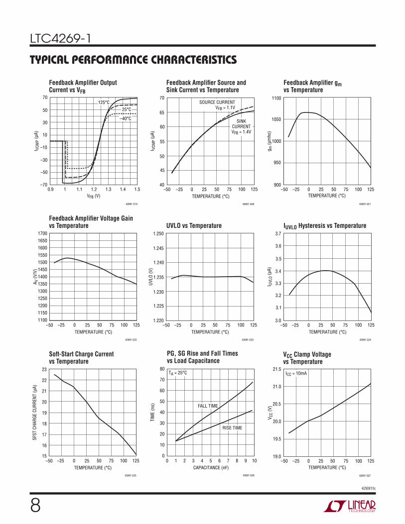
TYPICAL PERFORMANCE CHARACTERISTICS
Feedback Amplifi er Output Current vs VFB
Feedback Amplifi er Source and Sink Current vs Temperature
Feedback Amplifi er gm vs Temperature
Feedback Amplifi er Voltage Gain vs Temperature UVLO vs Temperature IUVLO Hysteresis vs Temperature
Soft-Start Charge Current vs Temperature
PG, SG Rise and Fall Times vs Load Capacitance
VCC Clamp Voltage vs Temperature
LTC4269-1
942691fc
TEMPERATURE (°C)
–50
t ON
(MIN
) (n
s)
330
25
42691 G28
300
280
–25 0 50
270
260
340
320
310
290
75 100 125
RtON(MIN) = 158k
TEMPERATURE (°C)
–500
t PG
DLY (
ns)
50
150
200
250
0 50 75
42691 G29
100
–25 25 100 125
300
RPGDLY = 16.9k
RPGDLY = 27.4k
TEMPERATURE (°C)
–50
t EN
DLY (
ns)
285
305
325
25 75
42691 G30
265
245
–25 0 50 100 125
225
205
RENDLY = 90k
TYPICAL PERFORMANCE CHARACTERISTICS
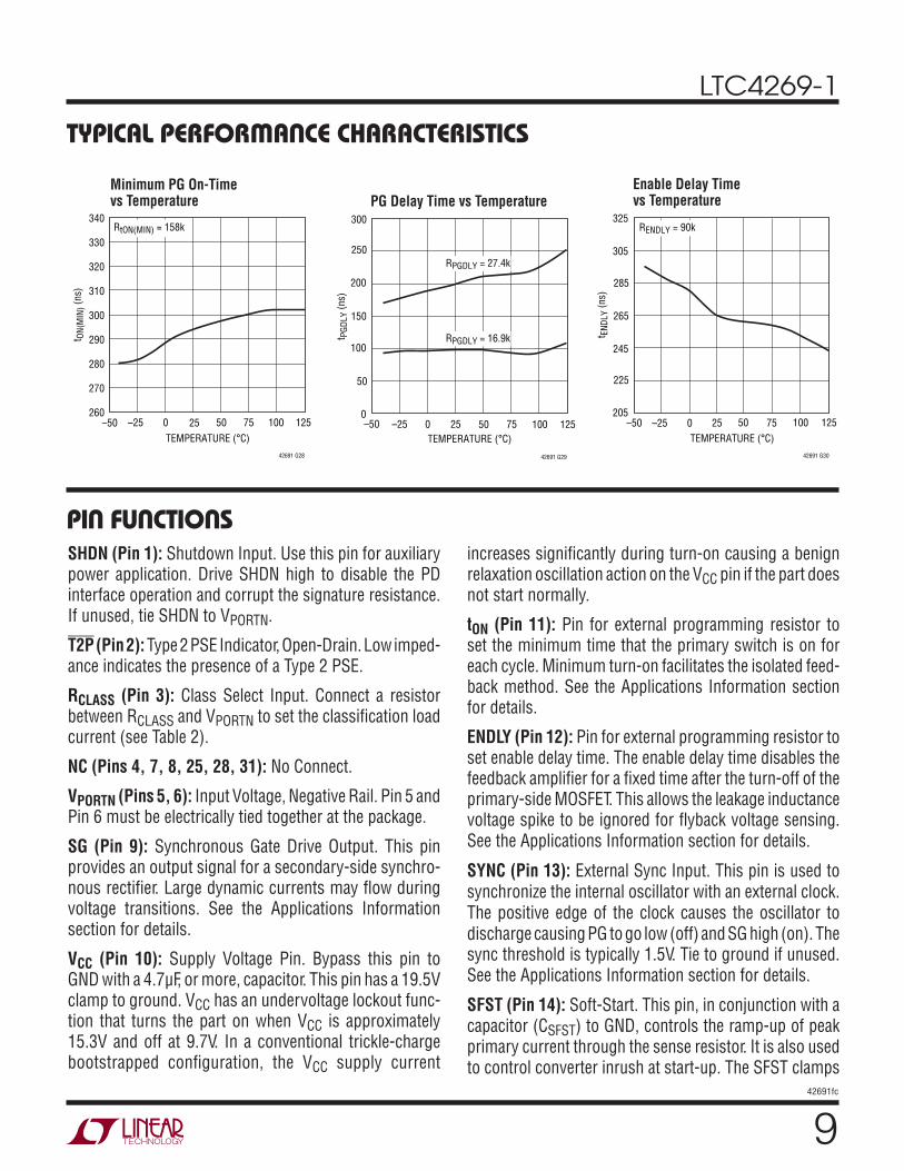
Minimum PG On-Time vs Temperature PG Delay Time vs Temperature
Enable Delay Time vs Temperature
PIN FUNCTIONSSHDN (Pin 1): Shutdown Input. Use this pin for auxiliary power application. Drive SHDN high to disable the PD interface operation and corrupt the signature resistance. If unused, tie SHDN to VPORTN.
T2P (Pin 2): Type 2 PSE Indicator, Open-Drain. Low imped-ance indicates the presence of a Type 2 PSE.
RCLASS (Pin 3): Class Select Input. Connect a resistor between RCLASS and VPORTN to set the classifi cation load current (see Table 2).
NC (Pins 4, 7, 8, 25, 28, 31): No Connect.
VPORTN (Pins 5, 6): Input Voltage, Negative Rail. Pin 5 and Pin 6 must be electrically tied together at the package.
SG (Pin 9): Synchronous Gate Drive Output. This pin provides an output signal for a secondary-side synchro-nous rectifi er. Large dynamic currents may fl ow during voltage transitions. See the Applications Information section for details.
VCC (Pin 10): Supply Voltage Pin. Bypass this pin to GND with a 4.7μF, or more, capacitor. This pin has a 19.5V clamp to ground. VCC has an undervoltage lockout func-tion that turns the part on when VCC is approximately 15.3V and off at 9.7V. In a conventional trickle-charge bootstrapped confi guration, the VCC supply current
increases signifi cantly during turn-on causing a benign relaxation oscillation action on the VCC pin if the part does not start normally.
tON (Pin 11): Pin for external programming resistor to set the minimum time that the primary switch is on for each cycle. Minimum turn-on facilitates the isolated feed-back method. See the Applications Information section for details.
ENDLY (Pin 12): Pin for external programming resistor to set enable delay time. The enable delay time disables the feedback amplifi er for a fi xed time after the turn-off of the primary-side MOSFET. This allows the leakage inductance voltage spike to be ignored for fl yback voltage sensing. See the Applications Information section for details.
SYNC (Pin 13): External Sync Input. This pin is used to synchronize the internal oscillator with an external clock. The positive edge of the clock causes the oscillator to discharge causing PG to go low (off) and SG high (on). The sync threshold is typically 1.5V. Tie to ground if unused. See the Applications Information section for details.
SFST (Pin 14): Soft-Start. This pin, in conjunction with a capacitor (CSFST) to GND, controls the ramp-up of peak primary current through the sense resistor. It is also used to control converter inrush at start-up. The SFST clamps
LTC4269-1
1042691fc
the VCMP voltage and thus limits peak current until soft-start is complete. The ramp time is approximately 70ms per μF of capacitance. Leave SFST open if not using the soft-start function.
OSC (Pin 15): Oscillator. This pin, in conjunction with an external capacitor (COSC) to GND, defi nes the controller oscillator frequency. The frequency is approximately 100kHz • 100/COSC (pF).
FB (Pin 16): Feedback Amplifi er Input. Feedback is usually sensed via a third winding and enabled during the fl yback period. This pin also sinks additional current to compensate for load current variation as set by the RCMP pin. Keep the Thevenin equivalent resistance of the feedback divider at roughly 3k.
VCMP (Pin 17): Frequency Compensation Control. VCMP is used for frequency compensation of the switcher con-trol loop. It is the output of the feedback amplifi er and the input to the current comparator. Switcher frequency compensation components are placed on this pin to GND. The voltage on this pin is proportional to the peak primary switch current. The feedback amplifi er output is enabled during the synchronous switch on time.
UVLO (Pin 18): Undervoltage Lockout. A resistive divider from VPORTP to this pin sets an undervoltage lockout based upon VPORTP level (not VCC). When the UVLO pin is below its threshold, the gate drives are disabled, but the part draws its normal quiescent current from VCC. The VCC undervoltage lockout supersedes this function, so VCC must be great enough to start the part.
The bias current on this pin has hysteresis such that the bias current is sourced when UVLO threshold is exceeded. This introduces a hysteresis at the pin equivalent to the bias current change times the impedance of the upper divider resistor. The user can control the amount of hysteresis by adjusting the impedance of the divider. Tie the UVLO pin to VCC if not using this function. See the Applications Information section for details. This pin is used for the UVLO function of the switching regulator. The PD interface section has an internal UVLO.
SENSE–, SENSE+ (Pins 19, 20): Current Sense Inputs. These pins are used to measure primary-side switch cur-rent through an external sense resistor. Peak primary-side
PIN FUNCTIONScurrent is used in the converter control loop. Make Kelvin connections to the sense resistor RSENSE to reduce noise problems. SENSE– connects to the GND side. At maximum current (VCMP at its maximum voltage) SENSE pins have 100mV threshold. The signal is blanked (ignored) during the minimum turn-on time.
CCMP (Pin 21): Load Compensation Capacitive Control. Connect a capacitor from CCMP to GND in order to reduce the effects of parasitic resistances in the feedback sensing path. A 0.1μF ceramic capacitor suffi ces for most applica-tions. Short this pin to GND when load compensation is not needed.
RCMP (Pin 22): Load Compensation Resistive Control. Connect a resistor from RCMP to GND in order to com-pensate for parasitic resistances in the feedback sensing path. In less demanding applications, this resistor is not needed and this pin can be left open. See the Applications Information section for details.
PGDLY (Pin 23): Primary Gate Delay Control. Connect an external programming resistor (RPGDLY) to set delay from synchronous gate turn-off to primary gate turn-on. See the Applications Information section for details.
PG (Pin 24): Primary Gate Drive. PG is the gate drive pin for the primary-side MOSFET switch. Large dynamic cur-rents fl ow during voltage transitions. See the Applications Information section for details.
VNEG (Pins 26, 27): System Negative Rail. Connects VNEG to VPORTN through an internal power MOSFET. Pin 26 and Pin 27 must be electrically tied together at the package.
PWRGD (Pin 29): Power Good Output, Open-Collector. High impedence signals power-up completion. PWRGD is referenced to VNEG and features a 14V clamp.
PWRGD (Pin 30): Complementary Power Good Output, Open-Drain. Low impedance signals power-up completion. PWRGD is referenced to VPORTN.
VPORTP (Pin 32): Positive Power Input. Tie to the input port power through the input diode bridge.
Exposed Pad (Pin 33): Ground. This is the negative rail connection for both signal ground and gate driver grounds of the fl yback controller. This pin should be connected to VNEG.
LTC4269-1
1142691fc
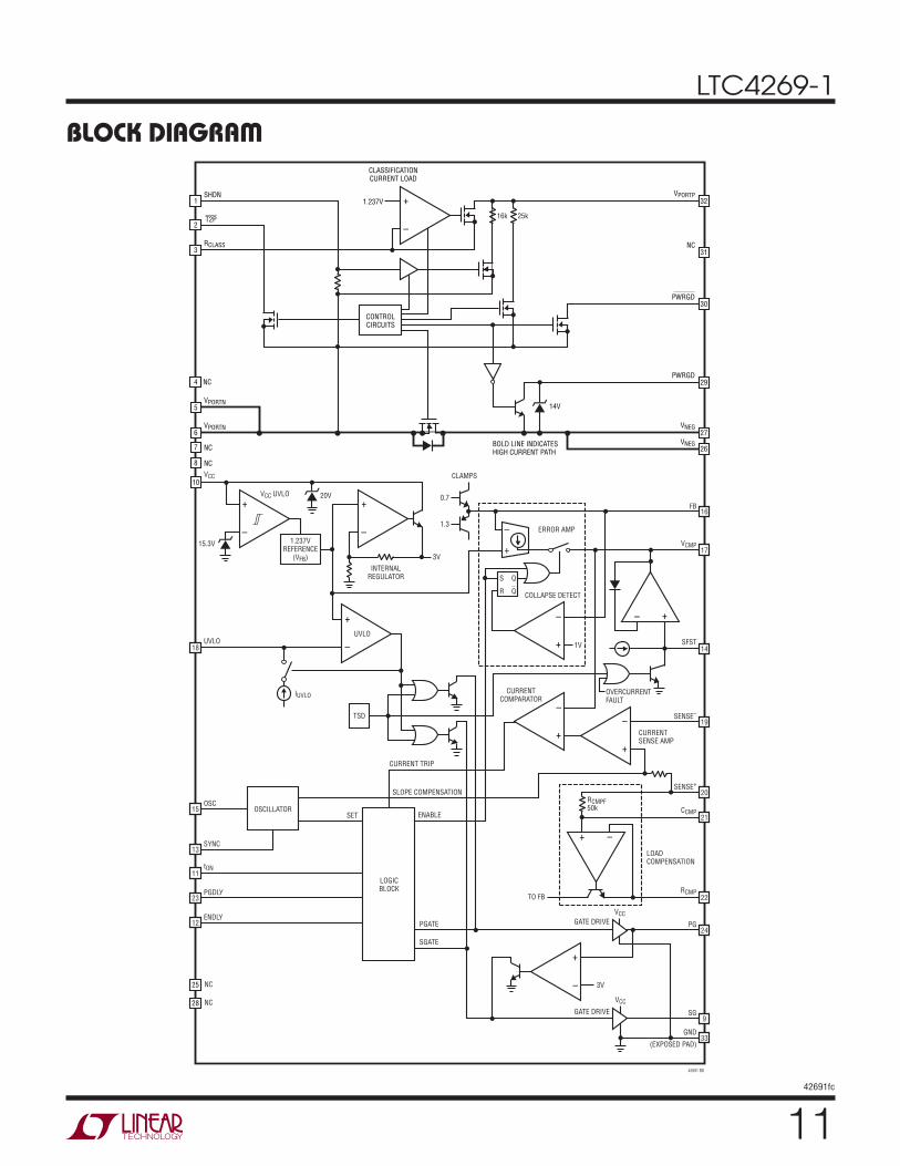
BLOCK DIAGRAM
19SENSE–
20SENSE+
CCMP
VCC
3V
TO FB
PGATE
SGATE
CURRENTSENSE AMP
RCMPF50k
LOADCOMPENSATION
–
+
–
+
–
+ –
+
–
+
– +
–+
15.3V
VCC UVLO
UVLO
IUVLO
18
OSC15
tON11
PGDLY23
ENDLY
NC
12
SYNC13
1.237VREFERENCE
(VFB)
INTERNALREGULATOR
UVLO
3V
COLLAPSE DETECT
ERROR AMP
CLAMPS
0.7
1.3
20V
+
–
S
R
Q
Q
1V
16FB
17VCMP
14SFST
TSD
CURRENT TRIP
SLOPE COMPENSATION
CURRENTCOMPARATOR
OVERCURRENTFAULT
LOGICBLOCK
–
+
–
+
21
RCMP
GATE DRIVE
22
PG24
SG9
GND
(EXPOSED PAD)33
OSCILLATORSET ENABLE
VCC
GATE DRIVE
BOLD LINE INDICATES HIGH CURRENT PATH
14V
32
T2P2
RCLASS3
NC4
SHDN
PWRGD
VPORTP
31NC
1
30
PWRGD29
25
NC28
VNEG
VNEG26
CONTROLCIRCUITS
CLASSIFICATIONCURRENT LOAD
1.237V
–
+
16k 25k
7
VPORTN
NC
8 NC
10VCC
6 27
42691 BD
VPORTN5
LTC4269-1
1242691fc
APPLICATIONS INFORMATIONOVERVIEW
Power over Ethernet (PoE) continues to gain popularity as more products are taking advantage of having DC power and high speed data available from a single RJ45 connector. As PoE continues to grow in the marketplace, Powered Device (PD) equipment vendors are running into the 13.0W power limit established by the IEEE 802.3af standard.
The IEE802.3at standard establishes a higher power allocation for Power over Ethernet while maintaining backwards compatibility with the existing IEEE 802.3af systems. Power sourcing equipment (PSE) and powered devices are distinguished as Type 1 complying with the IEEE 802.3af power levels, or Type 2 complying with the IEEE 802.3at power levels. The maximum available power of a Type 2 PD is 25.5W.
The IEEE 802.3at standard also establishes a new method of acquiring power classifi cation from a PD and communi-cating the presence of a Type 2 PSE. A Type 2 PSE has the option of acquiring PD power classifi cation by performing 2-event classifi cation (layer 1) or by communicating with the PD over the data line (layer 2). In turn, a Type 2 PD must be able to recognize both layers of communications and identify a Type 2 PSE.
The LTC4269-1 is specifi cally designed to support the front end of a PD that must operate under the IEEE 802.3at standard. In particular, the LTC4269-1 provides the T2P
indicator bit which recognizes 2-event classifi cation. This indicator bit may be used to alert the LTC4269-1 output load that a Type 2 PSE is present. With an internal signature resistor, classifi cation circuitry, inrush control, and thermal shutdown, the LTC4269-1 is a complete PD Interface solution capable of supporting in the next gen-eration PD applications.
MODES OF OPERATION
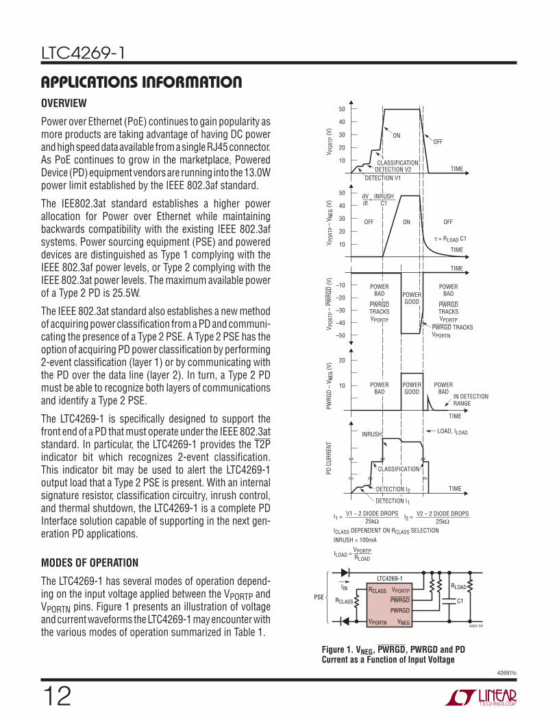
The LTC4269-1 has several modes of operation depend-ing on the input voltage applied between the VPORTP and VPORTN pins. Figure 1 presents an illustration of voltage and current waveforms the LTC4269-1 may encounter with the various modes of operation summarized in Table 1.
DETECTION V1
CLASSIFICATION
ONOFF
OFF
POWERBAD
OFFON
= RLOAD C1
PWRGD TRACKSVPORTN
DETECTION V2
50
TIME
40
30
VP
OR
TP (
V)
20
10
50
40
30
20
10TIME
VP
OR
TP
– V
NEG
(V
)
–10
TIME
–20
–30
VP
OR
TP –
PW
RG
D (
V)
PW
RG
D –
VN
EG
(V
)–40
–50
20
10
PD
CU
RR
EN
T
INRUSH
dVdt
INRUSHC1
=
POWERBAD
PWRGD
TRACKSVPORTP
PWRGD
TRACKSVPORTP
POWERBAD
POWERBAD
TIME
TIME
POWERGOOD
POWERGOOD
DETECTION I1
CLASSIFICATION
DETECTION I2
LOAD, ILOAD
42691 F01
ICLASS DEPENDENT ON RCLASS SELECTION
INRUSH = 100mA
I1 = V1 – 2 DIODE DROPS
25kΩ
ILOAD = VPORTP
RLOAD
I2 = V2 – 2 DIODE DROPS
25kΩ
VPORTP
PSE
IIN RLOAD
RCLASS C1
RCLASS
PWRGD
PWRGD
LTC4269-1
VNEGVPORTN
IN DETECTIONRANGE
Figure 1. VNEG, PWRGD, PWRGD and PD Current as a Function of Input Voltage
LTC4269-1
1342691fc
APPLICATIONS INFORMATIONTable 1. LTC4269-1 Modes of Operation as a Function of Input Voltage
VPORTP–VPORTN (V) LTC4269-1 MODES OF OPERATION
0V to 1.4V Inactive (Reset After 1st Classifi cation Event)
1.5V to 9.8V(5.4V to 9.8V)
25k Signature Resistor Detection Before 1st Classifi cation Event (Mark, 11k Signature Corrupt After 1st Classifi cation Event)
12.5V to ON/OFF* Classifi cation Load Current Active
ON/OFF* to 60V Inrush and Power Applied To PD Load
>71V Overvoltage Lockout, Classifi cation and Hot Swap Are Disabled
*ON/OFF includes hysteresis. Rising input threshold, 37.2V Max. Falling input threshold, 30V Min.
These modes satisfy the requirements defi ned in the IEEE 802.3af/IEEE 802.3at specifi cation.
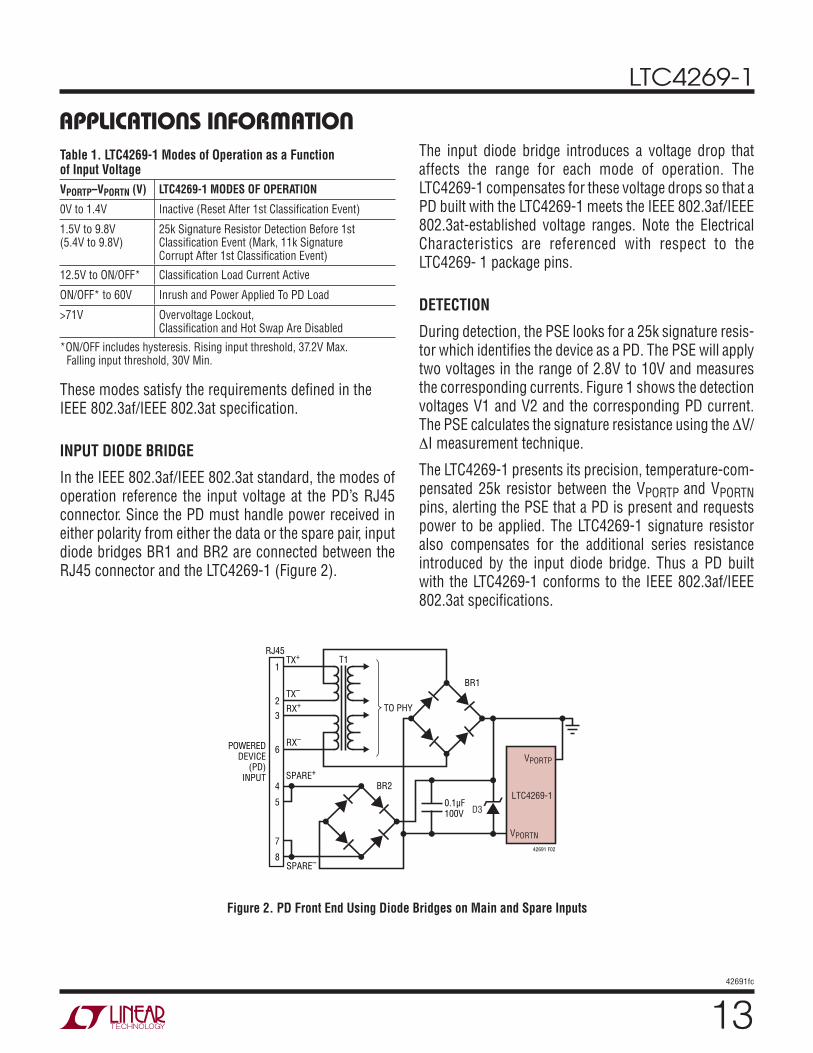
INPUT DIODE BRIDGE
In the IEEE 802.3af/IEEE 802.3at standard, the modes of operation reference the input voltage at the PD’s RJ45 connector. Since the PD must handle power received in either polarity from either the data or the spare pair, input diode bridges BR1 and BR2 are connected between the RJ45 connector and the LTC4269-1 (Figure 2).
The input diode bridge introduces a voltage drop that affects the range for each mode of operation. The LTC4269-1 compensates for these voltage drops so that a PD built with the LTC4269-1 meets the IEEE 802.3af/IEEE 802.3at-established voltage ranges. Note the Electrical Characteristics are referenced with respect to the LTC4269- 1 package pins.
DETECTION
During detection, the PSE looks for a 25k signature resis-tor which identifi es the device as a PD. The PSE will apply two voltages in the range of 2.8V to 10V and measures the corresponding currents. Figure 1 shows the detection voltages V1 and V2 and the corresponding PD current. The PSE calculates the signature resistance using the ΔV/ΔI measurement technique.
The LTC4269-1 presents its precision, temperature-com-pensated 25k resistor between the VPORTP and VPORTN pins, alerting the PSE that a PD is present and requests power to be applied. The LTC4269-1 signature resistor also compensates for the additional series resistance introduced by the input diode bridge. Thus a PD built with the LTC4269-1 conforms to the IEEE 802.3af/IEEE 802.3at specifi cations.
RX–
6
RX+
3
TX–
2
TX+RJ45
T1
POWEREDDEVICE
(PD)INPUT
42691 F02
1
7
8
5
4
SPARE–
SPARE+
TO PHY
BR2
0.1μF100V
BR1
D3
LTC4269-1
VPORTN
VPORTP
Figure 2. PD Front End Using Diode Bridges on Main and Spare Inputs
LTC4269-1
1442691fc
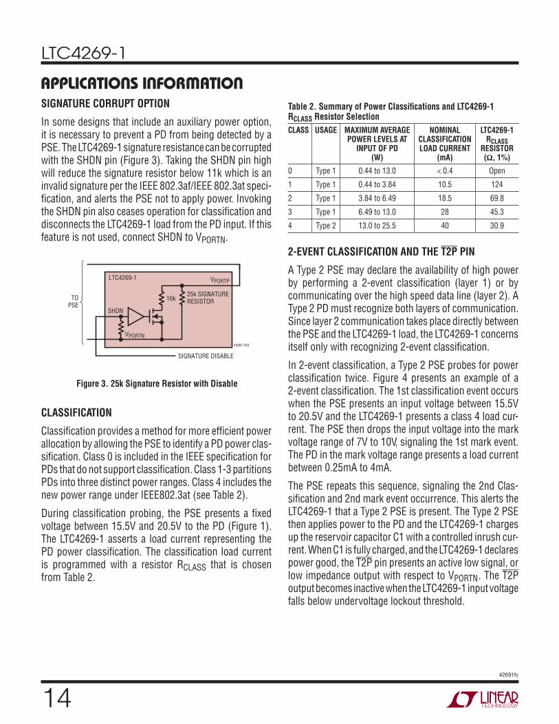
APPLICATIONS INFORMATIONSIGNATURE CORRUPT OPTION
In some designs that include an auxiliary power option, it is necessary to prevent a PD from being detected by a PSE. The LTC4269-1 signature resistance can be corrupted with the SHDN pin (Figure 3). Taking the SHDN pin high will reduce the signature resistor below 11k which is an invalid signature per the IEEE 802.3af/IEEE 802.3at speci-fi cation, and alerts the PSE not to apply power. Invoking the SHDN pin also ceases operation for classifi cation and disconnects the LTC4269-1 load from the PD input. If this feature is not used, connect SHDN to VPORTN.
Table 2. Summary of Power Classifi cations and LTC4269-1 RCLASS Resistor Selection
CLASS USAGE MAXIMUM AVERAGE POWER LEVELS AT
INPUT OF PD (W)
NOMINAL CLASSIFICATION LOAD CURRENT
(mA)
LTC4269-1 RCLASS
RESISTOR (Ω, 1%)
0 Type 1 0.44 to 13.0 < 0.4 Open
1 Type 1 0.44 to 3.84 10.5 124
2 Type 1 3.84 to 6.49 18.5 69.8
3 Type 1 6.49 to 13.0 28 45.3
4 Type 2 13.0 to 25.5 40 30.9
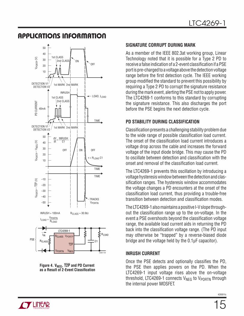
2-EVENT CLASSIFICATION AND THE T2P PIN
A Type 2 PSE may declare the availability of high power by performing a 2-event classifi cation (layer 1) or by communicating over the high speed data line (layer 2). A Type 2 PD must recognize both layers of communication. Since layer 2 communication takes place directly between the PSE and the LTC4269-1 load, the LTC4269-1 concerns itself only with recognizing 2-event classifi cation.
In 2-event classifi cation, a Type 2 PSE probes for power classifi cation twice. Figure 4 presents an example of a 2-event classifi cation. The 1st classifi cation event occurs when the PSE presents an input voltage between 15.5V to 20.5V and the LTC4269-1 presents a class 4 load cur-rent. The PSE then drops the input voltage into the mark voltage range of 7V to 10V, signaling the 1st mark event. The PD in the mark voltage range presents a load current between 0.25mA to 4mA.
The PSE repeats this sequence, signaling the 2nd Clas-sifi cation and 2nd mark event occurrence. This alerts the LTC4269-1 that a Type 2 PSE is present. The Type 2 PSE then applies power to the PD and the LTC4269-1 charges up the reservoir capacitor C1 with a controlled inrush cur-rent. When C1 is fully charged, and the LTC4269-1 declares power good, the T2P pin presents an active low signal, or low impedance output with respect to VPORTN. The T2P output becomes inactive when the LTC4269-1 input voltage falls below undervoltage lockout threshold.
Figure 3. 25k Signature Resistor with Disable
VPORTP
VPORTN
SHDN
LTC4269-1
SIGNATURE DISABLE
42691 F03
25k SIGNATURERESISTOR16kTO
PSE
CLASSIFICATION
Classifi cation provides a method for more effi cient power allocation by allowing the PSE to identify a PD power clas-sifi cation. Class 0 is included in the IEEE specifi cation for PDs that do not support classifi cation. Class 1-3 partitions PDs into three distinct power ranges. Class 4 includes the new power range under IEEE802.3at (see Table 2).
During classifi cation probing, the PSE presents a fi xed voltage between 15.5V and 20.5V to the PD (Figure 1). The LTC4269-1 asserts a load current representing the PD power classifi cation. The classifi cation load current is programmed with a resistor RCLASS that is chosen from Table 2.
LTC4269-1
1542691fc
APPLICATIONS INFORMATION
DETECTION V1
ONOFF
OFF OFFON
= RLOAD C1
TRACKSVPORTN
DETECTION V2
TIME
PD
CU
RR
EN
T
50
40
30
VP
OR
TP (
V)
20
10
40mA
50
40
30
20
10
TIME
VP
OR
TP
– V
NEG
(V
)
–10TIME
–20
–30
VP
OR
TP
– T
2P
(V
)
–40
–50
dVdt
INRUSHC1
=
42691 F04
INRUSH = 100mA RCLASS = 30.9Ω
ILOAD = VPORTN
RLOAD
VPORTP
PSE
IIN RLOAD
RCLASS C1
RCLASS
T2P
LTC4269-1
VNEGVPORTN
1st CLASS
1st MARK 2nd MARK
DETECTION V1DETECTION V2
1st MARK 2nd MARK
2nd CLASS
1st CLASS
2nd CLASS
LOAD, ILOAD
INRUSH
Figure 4. VNEG, T2P and PD Current as a Result of 2-Event Classifi cation
SIGNATURE CORRUPT DURING MARK
As a member of the IEEE 802.3at working group, Linear Technology noted that it is possible for a Type 2 PD to receive a false indication of a 2-event classifi cation if a PSE port is pre-charged to a voltage above the detection voltage range before the fi rst detection cycle. The IEEE working group modifi ed the standard to prevent this possibility by requiring a Type 2 PD to corrupt the signature resistance during the mark event, alerting the PSE not to apply power. The LTC4269-1 conforms to this standard by corrupting the signature resistance. This also discharges the port before the PSE begins the next detection cycle.
PD STABILITY DURING CLASSIFICATION
Classifi cation presents a challenging stability problem due to the wide range of possible classifi cation load current. The onset of the classifi cation load current introduces a voltage drop across the cable and increases the forward voltage of the input diode bridge. This may cause the PD to oscillate between detection and classifi cation with the onset and removal of the classifi cation load current.
The LTC4269-1 prevents this oscillation by introducing a voltage hysteresis window between the detection and clas-sifi cation ranges. The hysteresis window accommodates the voltage changes a PD encounters at the onset of the classifi cation load current, thus providing a trouble-free transition between detection and classifi cation modes.
The LTC4269-1 also maintains a positive I-V slope through-out the classifi cation range up to the on-voltage. In the event a PSE overshoots beyond the classifi cation voltage range, the available load current aids in returning the PD back into the classifi cation voltage range. (The PD input may otherwise be “trapped” by a reverse-biased diode bridge and the voltage held by the 0.1μF capacitor).
INRUSH CURRENT
Once the PSE detects and optionally classifi es the PD, the PSE then applies powers on the PD. When the LTC4269-1 input voltage rises above the on-voltage threshold, LTC4269-1 connects VNEG to VPORTN through the internal power MOSFET.
LTC4269-1
1642691fc
APPLICATIONS INFORMATIONTo control the power-on surge currents in the system, the LTC4269-1 provides a fi xed inrush current, allowing C1 to ramp up to the line voltage in a controlled manner.
The LTC4269-1 keeps the PD inrush current below the PSE current limit to provide a well controlled power-up characteristic that is independent of the PSE behavior. This ensures a PD using the LTC4269-1 interoperability with any PSE.
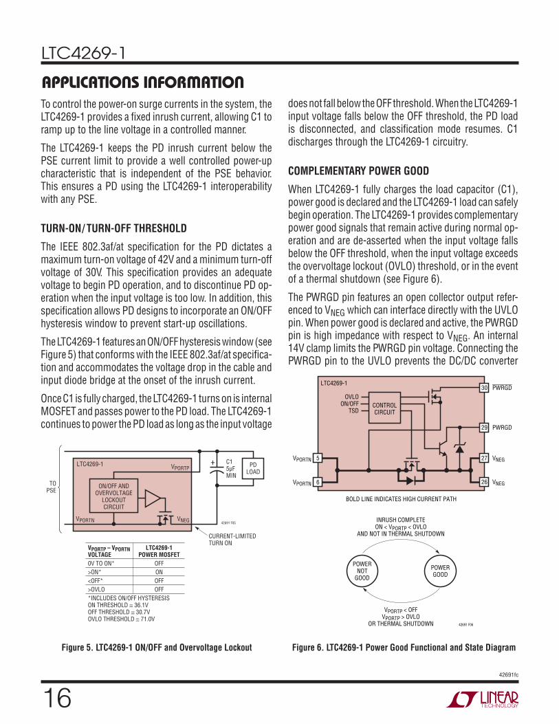
TURN-ON/ TURN-OFF THRESHOLD
The IEEE 802.3af/at specifi cation for the PD dictates a maximum turn-on voltage of 42V and a minimum turn-off voltage of 30V. This specifi cation provides an adequate voltage to begin PD operation, and to discontinue PD op-eration when the input voltage is too low. In addition, this specifi cation allows PD designs to incorporate an ON/OFF hysteresis window to prevent start-up oscillations.
The LTC4269-1 features an ON/OFF hysteresis window (see Figure 5) that conforms with the IEEE 802.3af/at specifi ca-tion and accommodates the voltage drop in the cable and input diode bridge at the onset of the inrush current.
Once C1 is fully charged, the LTC4269-1 turns on is internal MOSFET and passes power to the PD load. The LTC4269-1 continues to power the PD load as long as the input voltage
Figure 5. LTC4269-1 ON/OFF and Overvoltage Lockout
VPORTP
C15μFMIN
VPORTN VNEG
LTC4269-1
42691 F05
TOPSE
ON/OFF ANDOVERVOLTAGE
LOCKOUTCIRCUIT
PDLOAD
CURRENT-LIMITEDTURN ON
+
VPORTP – VPORTN LTC4269-1VOLTAGE POWER MOSFET
0V TO ON* OFF
>ON* ON
<OFF* OFF
>OVLO OFF
*INCLUDES ON/OFF HYSTERESISON THRESHOLD 36.1VOFF THRESHOLD 30.7VOVLO THRESHOLD 71.0V
Figure 6. LTC4269-1 Power Good Functional and State Diagram
42691 F06
BOLD LINE INDICATES HIGH CURRENT PATH
PWRGD
POWERNOT
GOOD
INRUSH COMPLETEON < VPORTP < OVLO
AND NOT IN THERMAL SHUTDOWN
VPORTP < OFFVPORTP > OVLO
OR THERMAL SHUTDOWN
POWERGOOD
29
PWRGDLTC4269-1
30
VNEG27
VNEG26VPORTN 6
VPORTN
OVLOON/OFF
TSD
5
CONTROLCIRCUIT
does not fall below the OFF threshold. When the LTC4269-1 input voltage falls below the OFF threshold, the PD load is disconnected, and classifi cation mode resumes. C1 discharges through the LTC4269-1 circuitry.
COMPLEMENTARY POWER GOOD
When LTC4269-1 fully charges the load capacitor (C1), power good is declared and the LTC4269-1 load can safely begin operation. The LTC4269-1 provides complementary power good signals that remain active during normal op-eration and are de-asserted when the input voltage falls below the OFF threshold, when the input voltage exceeds the overvoltage lockout (OVLO) threshold, or in the event of a thermal shutdown (see Figure 6).
The PWRGD pin features an open collector output refer-enced to VNEG which can interface directly with the UVLO pin. When power good is declared and active, the PWRGD pin is high impedance with respect to VNEG. An internal 14V clamp limits the PWRGD pin voltage. Connecting the PWRGD pin to the UVLO prevents the DC/DC converter
LTC4269-1
1742691fc
from commencing operation before the PD interface completely charges the reservoir capacitor, C1.
The active low PWRGD pin connects to an internal, open-drain MOSFET referenced to VPORTN and may be used as an indicator bit when power good is declared and active. The PWRGD pin is low impedance with respect to VPORTN.
PWRGD PIN WHEN SHDN IS INVOKED
In PD applications where an auxiliary power supply invokes the SHDN feature, the PWRGD pin becomes high imped-ance. This prevents the PWRGD pin that is connected to the UVLO pin from interfering with the DC/DC converter operations when powered by an auxiliary power supply.
OVERVOLTAGE LOCKOUT
The LTC4269-1 includes an overvoltage lockout (OVLO) feature (Figure 6) which protects the LTC4269-1 and its load from an overvoltage event. If the input voltage ex-ceeds the OVLO threshold, the LTC4269-1 discontinues PD operation. Normal operations resume when the input voltage falls below the OVLO threshold and when C1 is charged up.
THERMAL PROTECTION
The IEEE 802.3af/at specifi cation requires a PD to withstand any applied voltage from 0V to 57V indefi nitely. However, there are several possible scenarios where a PD may encounter excessive heating.
During classifi cation, excessive heating may occur if the PSE exceeds the 75ms probing time limit. At turn-on, when the load capacitor begins to charge, the instantaneous power dissipated by the PD interface can be large before it reaches the line voltage. And if the PD experiences a fast input positive voltage step in its operational mode (for example, from 37V to 57V), the instantaneous power dissipated by the PD Interface can be large.
The LTC4269-1 includes a thermal protection feature which protects the LTC4269-1 from excessive heating. If the LTC4269-1 junction temperature exceeds the over-temperature threshold, the LTC4269-1 discontinues PD
operations and power good becomes inactive. Normal operation resumes when the junction temperature falls below the overtemperature threshold and when C1 is charged up.
EXTERNAL INTERFACE AND COMPONENT SELECTION
Transformer
Nodes on an Ethernet network commonly interface to the outside world via an isolation transformer. For PDs, the isolation transformer must also include a center tap on the RJ45 connector side (see Figure 7).
The increased current levels in a Type 2 PD over a Type 1increase the current imbalance in the magnetics which can interfere with data transmission. In addition, proper termination is also required around the transformer to provide correct impedance matching and to avoid radiated and conducted emissions. Transformer vendors such as Bel Fuse, Coilcraft, Halo, Pulse, and Tyco (Table 4) can assist in selecting an appropriate isolation transformer and proper termination methods.
Table 4. Power over Ethernet Transformer Vendors
VENDOR CONTACT INFORMATION
Bel Fuse Inc. 206 Van Vorst StreetJersey City, NJ 07302Tel: 201-432-0463www.belfuse.com
Coilcraft Inc. 1102 Silver Lake RoadGary, IL 60013Tel: 847-639-6400www.coilcraft.com
Halo Electronics 1861 Landings DriveMountain View, CA 94043Tel: 650-903-3800www.haloelectronics.com
PCA Electronics 16799 Schoenborn StreetNorth Hills, CA 91343Tel: 818-892-0761www.pca.com
Pulse Engineering 12220 World Trade DriveSan Diego, CA 92128Tel: 858-674-8100www.pulseeng.com
Tyco Electronics 308 Constitution DriveMenlo Park, CA 94025-1164Tel: 800-227-7040www.circuitprotection.com
APPLICATIONS INFORMATION
LTC4269-1
1842691fc
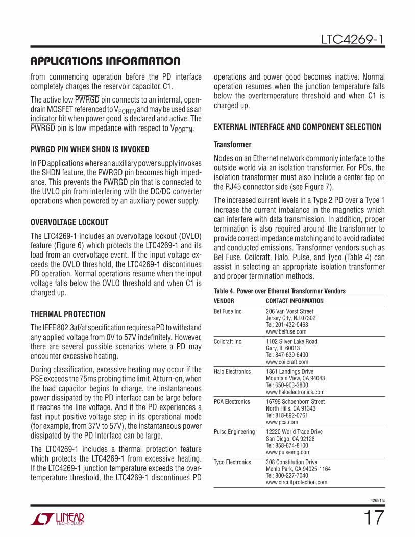
Input Diode Bridge
Figure 2 shows how two diode bridges are typically con-nected in a PD application. One bridge is dedicated to the data pair while the other bridge is dedicated to the spare pair. The LTC4269-1 supports the use of either silicon or Schottky input diode bridges. However, there are trade-offs in the choice of diode bridges.
An input diode bridge must be rated above the maximum current the PD application will encounter at the tempera-ture the PD will operate. Diode bridge vendors typically call out the operating current at room temperature, but derate the maximum current with increasing temperature. Consult the diode bridge vendors for the operating current derating curve.
A silicon diode bridge can consume over 4% of the available power in some PD applications. Using Schottky diodes can help reduce the power loss with a lower forward voltage.
A Schottky bridge may not be suitable for some high temperature PD application. The leakage current has a voltage dependency that can reduce the perceived signature resistance. In addition, the IEEE 802.3af/at specifi cation mandates the leakage back-feeding through the unused bridge cannot generate more than 2.8V across a 100k resistor when a PD is powered with 57V.
Sharing Input Diode Bridges
At higher temperatures, a PD design may be forced to consider larger bridges in a bigger package because the maximum operating current for the input diode bridge is drastically derated. The larger package may not be accept-able in some space-limited environments.
One solution to consider is to reconnect the diode bridges so that only one of the four diodes conducts current in each package. This confi guration extends the maximum operating current while maintaining a smaller package profi le. Figure 7 shows how to reconnect the two diode bridges. Consult the diode bridge vendors for the derating curve when only one of four diodes is in operation.
Input Capacitor
The IEEE 802.3af/at standard includes an impedance requirement in order to implement the AC disconnect function. A 0.1μF capacitor (C14 in Figure 7) is used to meet this AC impedance requirement.
Input Series Resistance
Linear Technology has seen the customer community cable discharge requirements increase by nearly 500,000 times the original test levels. The PD must survive and operate
APPLICATIONS INFORMATION
14
13
12
1
2
3
RX–
6
RX+
3
TX–
2
TX+RJ45
T1
COILCRAFTETHI - 230LD
42691 F07
1
7
8
5
4
10
9
11
5
6
4
D3SMAJ58A
TVS
BR1HD01
10Ω
BR2HD01
TO PHY
VPORTP
LTC4269-1C1
VPORTN VNEG
SPARE–
SPARE+
C140.1μF100V
Figure 7. PD Front-End with Isolation Transformer, Diode Bridges, Capacitors, and a Transient Voltage Suppressor (TVS).
LTC4269-1
1942691fc
reliably not only when an initially charged cable connects and dissipates the energy through the PD front end, but also when the electrical power system grounds are subject to very high energy events (e.g. lightning strikes).
In these high energy events, adding 10Ω series resistance into the VPORTP pin greatly improves the robustness of the LTC4269-1 based PD. (See Figure 7) The TVS limits the voltage across the port while the 10Ω and 0.1μF ca-pacitance reduces the edge rate the LT4269-1 encounters across its pin. The added10Ω series resistance does not operationally affect the LTC4269-1 PD interface nor does it affect its compliance with the IEEE802.3 standard.
Transient Voltage Suppressor
The LTC4269-1 specifi es an absolute maximum voltage of 100V and is designed to tolerate brief overvoltage events. However, the pins that interface to the outside world can rou-tinely see excessive peak voltages. To protect the LTC4269-1, install a transient voltage suppressor (D3) between the input diode bridge and the LTC4269-1 as shown in Figure 7.
A SMAJ58A is recommended for typical PD applications. However, a SMBJ58A may be preferred in applications where the PD front end must absorb higher energy dis-charge events.
Classifi cation Resistor (RCLASS)
The RCLASS resistor sets the classifi cation load current, cor-responding to the PD power classifi cation. Select the value of RCLASS from Table 2 and connect the resistor between the RCLASS and VPORTN pins as shown in Figure 4, or fl oat the RCLASS pin if the classifi cation load current is not re-quired. The resistor tolerance must be 1% or better to avoid degrading the overall accuracy of the classifi cation circuit.
Load Capacitor
The IEEE 802.3af/at specifi cation requires that the PD maintains a minimum load capacitance of 5μF and does not specify a maximum load capacitor. However, if the load capacitor is too large, there may be a problem with inadvertent power shutdown by the PSE.
This occurs when the PSE voltage drops quickly. The input diode bridge reverses bias, and the PD load momentarily powers off the load capacitor. If the PD does not draw power within the PSE’s 300ms disconnection delay, the PSE may remove power from the PD. Thus, it is necessary to evaluate the load current and capacitance to ensure that an inadvertent shutdown cannot occur.
The load capacitor can store signifi cant energy when fully charged. The PD design must ensure that this energy is not inadvertently dissipated in the LTC4269-1. For example, if the VPORTP pin shorts to VPORTN while the capacitor is charged, current will fl ow through the parasitic body diode of the internal MOSFET and may cause permanent damage to the LTC4269-1.
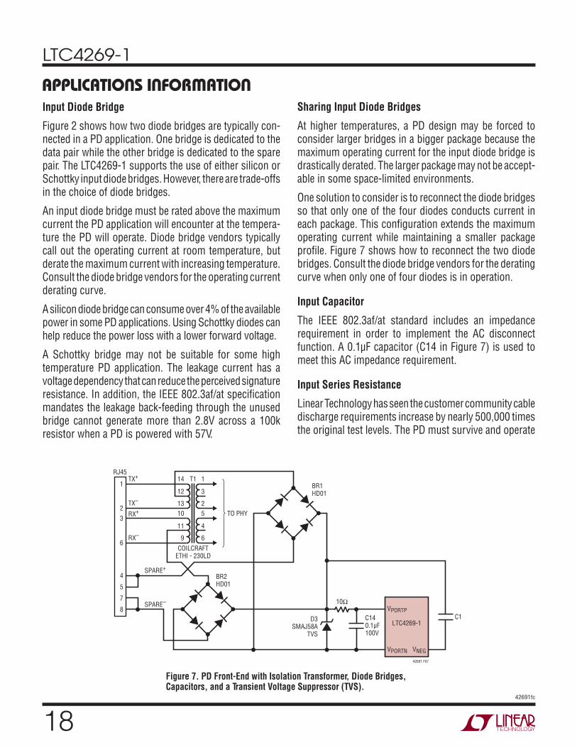
T2P Interface
When a 2-event classifi cation sequence successfully completes, the LTC4269-1 recognizes this sequence, and provides an indicator bit, declaring the presence of a Type 2 PSE. The open-drain output provides the option to use this signal to communicate to the LTC4269-1 load, or to leave the pin unconnected.
Figure 8 shows two interface options using the T2P pin and the opto-isolator. The T2P pin is active low and con-nects to an opto-isolator to communicate across the DC/DC converter isolation barrier. The pull-up resistor RP is sized according to the requirements of the opto-isolator
APPLICATIONS INFORMATION
42691 F08
OPTION 1: SERIES CONFIGURATION FOR ACTIVE LOW/LOW IMPEDANCE OUTPUT
–54V
TOPSE
RP
TO PD LOAD
VPORTP
LTC4269-1
VPORTN T2P
V+
OPTION 2: SHUNT CONFIGURATION FOR ACTIVE HIGH/OPEN COLLECTOR OUTPUT
–54V
TOPSE
RP
TO PD LOAD
VPORTP
LTC4269-1
VPORTN
T2P
V+
Figure 8. T2P Interface Examples
LTC4269-1
2042691fc
operating current, the pull-down capability of the T2P pin, and the choice of V+. V+ for example can come from the PoE supply rail (which the LTC4269-1 VPORTP is tied to), or from the voltage source that supplies power to the DC/DC converter. Option 1 has the advantage of not drawing power unless T2P is declared active.
Shutdown Interface
To corrupt the signature resistance, the SHDN pin can be driven high with respect to VPORTN. If unused, connect SHDN directly to VPORTN.
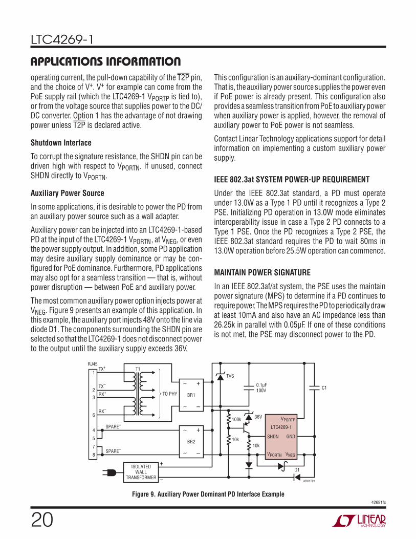
Auxiliary Power Source
In some applications, it is desirable to power the PD from an auxiliary power source such as a wall adapter.
Auxiliary power can be injected into an LTC4269-1-based PD at the input of the LTC4269-1 VPORTN, at VNEG, or even the power supply output. In addition, some PD application may desire auxiliary supply dominance or may be con-fi gured for PoE dominance. Furthermore, PD applications may also opt for a seamless transition — that is, without power disruption — between PoE and auxiliary power.
The most common auxiliary power option injects power at VNEG. Figure 9 presents an example of this application. In this example, the auxiliary port injects 48V onto the line via diode D1. The components surrounding the SHDN pin are selected so that the LTC4269-1 does not disconnect power to the output until the auxiliary supply exceeds 36V.
This confi guration is an auxiliary-dominant confi guration. That is, the auxiliary power source supplies the power even if PoE power is already present. This confi guration also provides a seamless transition from PoE to auxiliary power when auxiliary power is applied, however, the removal of auxiliary power to PoE power is not seamless.
Contact Linear Technology applications support for detail information on implementing a custom auxiliary power supply.
IEEE 802.3at SYSTEM POWER-UP REQUIREMENT
Under the IEEE 802.3at standard, a PD must operate under 13.0W as a Type 1 PD until it recognizes a Type 2 PSE. Initializing PD operation in 13.0W mode eliminates interoperability issue in case a Type 2 PD connects to a Type 1 PSE. Once the PD recognizes a Type 2 PSE, the IEEE 802.3at standard requires the PD to wait 80ms in 13.0W operation before 25.5W operation can commence.
MAINTAIN POWER SIGNATURE
In an IEEE 802.3af/at system, the PSE uses the maintain power signature (MPS) to determine if a PD continues to require power. The MPS requires the PD to periodically draw at least 10mA and also have an AC impedance less than 26.25k in parallel with 0.05μF. If one of these conditions is not met, the PSE may disconnect power to the PD.
APPLICATIONS INFORMATION
Figure 9. Auxiliary Power Dominant PD Interface Example
T1
42691 F09
TVS
TO PHY
36V100k
10k
10k
D1
BR1
+
–
BR2
+
–
0.1μF100V
C1
VPORTP
LTC4269-1
VPORTN
SHDN
VNEG
GND
+
–
ISOLATEDWALL
TRANSFORMER
RX–
6
RX+
3
TX–
2
TX+RJ45
1
7
8
5
4
SPARE–
SPARE+
LTC4269-1
2142691fc
SWITCHING REGULATOR OVERVIEW
The LTC4269-1 includes a current mode converter designed specifi cally for use in an isolated fl yback topology employing synchronous rectifi cation. The LTC4269-1 operation is similar to traditional current mode switchers. The major difference is that output voltage feedback is derived via sensing the output voltage through the transformer. This precludes the need of an opto-isolator in isolated designs, thus greatly improving dynamic response and reliability. The LTC4269-1 has a unique feedback amplifi er that samples a transformer winding voltage during the fl yback period and uses that voltage to control output voltage. The internal blocks are similar to many current mode controllers. The differences lie in the feedback amplifi er and load compensation circuitry. The logic block also contains circuitry to control the special dynamic requirements of fl yback control. For more information on the basics of current mode switcher/controllers and isolated fl yback converters see Application Note 19.
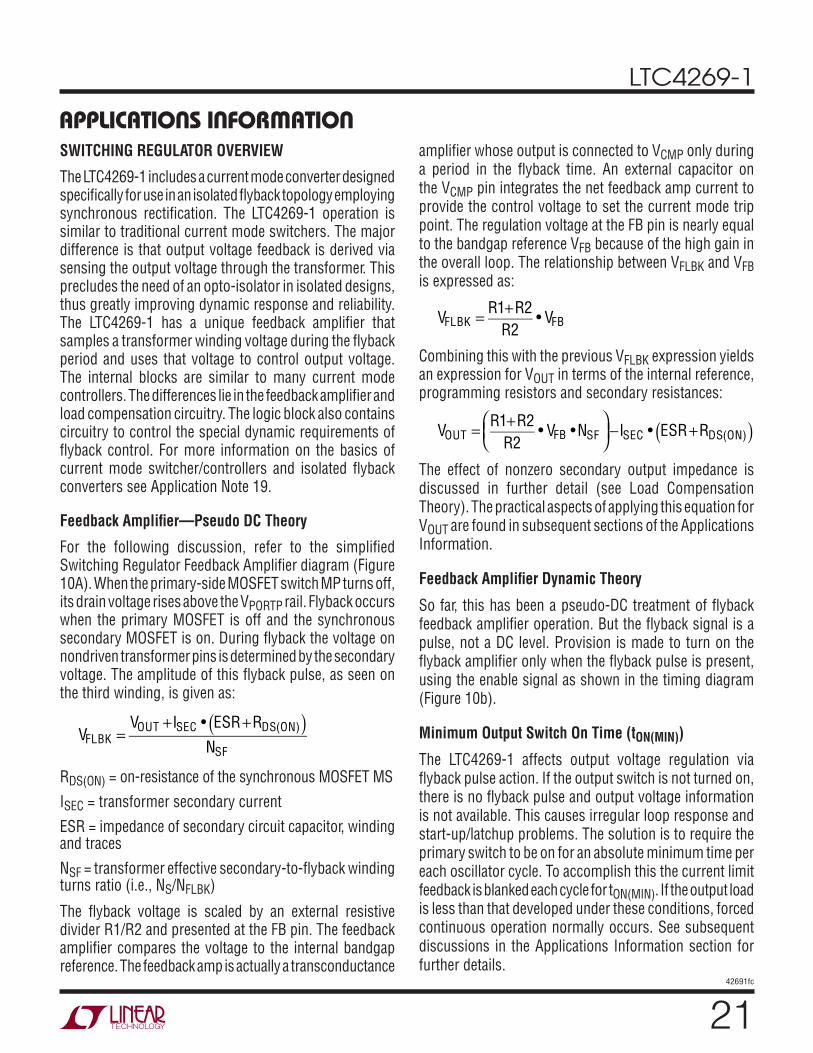
Feedback Amplifi er—Pseudo DC Theory
For the following discussion, refer to the simplifi ed Switching Regulator Feedback Amplifi er diagram (Figure 10A). When the primary-side MOSFET switch MP turns off, its drain voltage rises above the VPORTP rail. Flyback occurs when the primary MOSFET is off and the synchronous secondary MOSFET is on. During fl yback the voltage on nondriven transformer pins is determined by the secondary voltage. The amplitude of this fl yback pulse, as seen on the third winding, is given as:
VFLBK =VOUT +ISEC • ESR+RDS(ON)( )
NSF
RDS(ON) = on-resistance of the synchronous MOSFET MS
ISEC = transformer secondary current
ESR = impedance of secondary circuit capacitor, winding and traces
NSF = transformer effective secondary-to-fl yback winding turns ratio (i.e., NS/NFLBK)
The fl yback voltage is scaled by an external resistive divider R1/R2 and presented at the FB pin. The feedback amplifi er compares the voltage to the internal bandgap reference. The feedback amp is actually a transconductance
APPLICATIONS INFORMATIONamplifi er whose output is connected to VCMP only during a period in the fl yback time. An external capacitor on the VCMP pin integrates the net feedback amp current to provide the control voltage to set the current mode trip point. The regulation voltage at the FB pin is nearly equal to the bandgap reference VFB because of the high gain in the overall loop. The relationship between VFLBK and VFB is expressed as:
VFLBK = R1+R2
R2• VFB
Combining this with the previous VFLBK expression yields an expression for VOUT in terms of the internal reference, programming resistors and secondary resistances:
VOUT = R1+R2
R2• VFB •NSF
⎛⎝⎜
⎞⎠⎟−ISEC • ESR+RDS(ON)( )
The effect of nonzero secondary output impedance is discussed in further detail (see Load Compensation Theory). The practical aspects of applying this equation for VOUT are found in subsequent sections of the Applications Information.
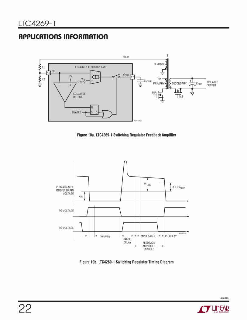
Feedback Amplifi er Dynamic Theory
So far, this has been a pseudo-DC treatment of fl yback feedback amplifi er operation. But the fl yback signal is a pulse, not a DC level. Provision is made to turn on the fl yback amplifi er only when the fl yback pulse is present, using the enable signal as shown in the timing diagram (Figure 10b).
Minimum Output Switch On Time (tON(MIN))
The LTC4269-1 affects output voltage regulation via fl yback pulse action. If the output switch is not turned on, there is no fl yback pulse and output voltage information is not available. This causes irregular loop response and start-up/latchup problems. The solution is to require the primary switch to be on for an absolute minimum time per each oscillator cycle. To accomplish this the current limit feedback is blanked each cycle for tON(MIN). If the output load is less than that developed under these conditions, forced continuous operation normally occurs. See subsequent discussions in the Applications Information section for further details.
LTC4269-1
2242691fc
APPLICATIONS INFORMATION
+
–
VFB1.237V
ENABLE
COLLAPSEDETECT
1V
LTC4269-1 FEEDBACK AMP
FB
R1
R2
16
17VCMP
VIN
PRIMARY
FLYBACK
SECONDARY•
•
•
MP
T1VFLBK
MS
CVCMP
42691 F10a
COUTISOLATEDOUTPUT
+
S
R
Q
– +
PRIMARY-SIDEMOSFET DRAIN
VOLTAGE
PG VOLTAGE
SG VOLTAGE
VIN
tON(MIN)ENABLEDELAY
MIN ENABLE
FEEDBACKAMPLIFIERENABLED
PG DELAY42691 F10b
VFLBK0.8 • VFLBK
Figure 10a. LTC4269-1 Switching Regulator Feedback Amplifi er
Figure 10b. LTC4269-1 Switching Regulator Timing Diagram
LTC4269-1
2342691fc
Enable Delay Time (ENDLY)
The fl yback pulse appears when the primary-side switch shuts off. However, it takes a fi nite time until the transformer primary-side voltage waveform represents the output voltage. This is partly due to rise time on the primary-side MOSFET drain node, but, more importantly, is due to transformer leakage inductance. The latter causes a voltage spike on the primary side, not directly related to output voltage. Some time is also required for internal settling of the feedback amplifi er circuitry. In order to maintain immunity to these phenomena, a fi xed delay is introduced between the switch turn-off command and the enabling of the feedback amplifi er. This is termed “enable delay.” In certain cases where the leakage spike is not suffi ciently settled by the end of the enable delay period, regulation error may result. See the subsequent sections for further details.
Collapse Detect
Once the feedback amplifi er is enabled, some mechanism is then required to disable it. This is accomplished by a collapse detect comparator, which compares the fl yback voltage (FB) to a fi xed reference, nominally 80% of VFB. When the fl yback waveform drops below this level, the feedback amplifi er is disabled.
Minimum Enable Time
The feedback amplifi er, once enabled, stays on for a fi xed minimum time period, termed “minimum enable time.” This prevents lockup, especially when the output voltage is abnormally low, e.g., during start-up. The minimum enable time period ensures that the VCMP node is able to “pump up” and increase the current mode trip point to the level where the collapse detect system exhibits proper operation. This time is set internally.
Effects of Variable Enable Period
The feedback amplifi er is enabled during only a portion of the cycle time. This can vary from the fi xed minimum enable time described to a maximum of roughly the off switch time minus the enable delay time. Certain parameters of feedback amp behavior are directly affected by the variable enable period. These include effective transconductance and VCMP node slew rate.
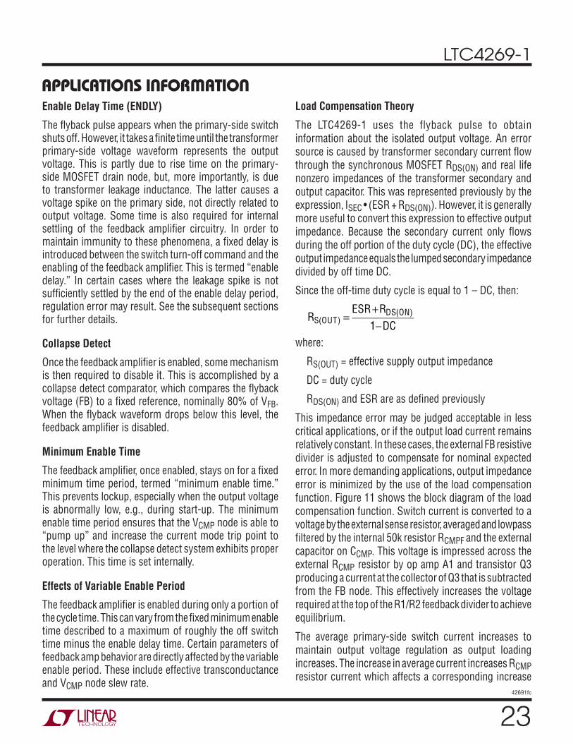
Load Compensation Theory
The LTC4269-1 uses the flyback pulse to obtain information about the isolated output voltage. An error source is caused by transformer secondary current fl ow through the synchronous MOSFET RDS(ON) and real life nonzero impedances of the transformer secondary and output capacitor. This was represented previously by the expression, ISEC • (ESR + RDS(ON)). However, it is generally more useful to convert this expression to effective output impedance. Because the secondary current only fl ows during the off portion of the duty cycle (DC), the effective output impedance equals the lumped secondary impedance divided by off time DC.
Since the off-time duty cycle is equal to 1 – DC, then:
RS(OUT) =
ESR+RDS(ON)
1−DC
where:
RS(OUT) = effective supply output impedance
DC = duty cycle
RDS(ON) and ESR are as defi ned previously
This impedance error may be judged acceptable in less critical applications, or if the output load current remains relatively constant. In these cases, the external FB resistive divider is adjusted to compensate for nominal expected error. In more demanding applications, output impedance error is minimized by the use of the load compensation function. Figure 11 shows the block diagram of the load compensation function. Switch current is converted to a voltage by the external sense resistor, averaged and lowpass fi ltered by the internal 50k resistor RCMPF and the external capacitor on CCMP. This voltage is impressed across the external RCMP resistor by op amp A1 and transistor Q3 producing a current at the collector of Q3 that is subtracted from the FB node. This effectively increases the voltage required at the top of the R1/R2 feedback divider to achieve equilibrium.
The average primary-side switch current increases to maintain output voltage regulation as output loading increases. The increase in average current increases RCMP resistor current which affects a corresponding increase
APPLICATIONS INFORMATION
LTC4269-1
2442691fc
in sensed output voltage, compensating for the IR drops. Assuming relatively fi xed power supply effi ciency, Eff, power balance gives:
POUT = Eff • PIN
VOUT • IOUT = Eff • VIN • IIN
Average primary-side current is expressed in terms of output current as follows:
IIN = K1•IOUT
where:
K1=VOUT
VIN •Eff
So, the effective change in VOUT target is:
ΔVOUT = K1•RSENSE
RCMP
•R1•NSF • ΔIOUT
thus :
ΔVOUT
ΔIOUT
= K1•RSENSE
RCMP
•R1•NSF
where:
K1 = dimensionless variable related to VIN, VOUT and ef-
fi ciency, as previously explained
RSENSE = external sense resistor
Nominal output impedance cancellation is obtained by
equating this expression with RS(OUT):
K1•RSENSE
RCMP
•R1•NSF =ESR+RDS(ON)
1−DC
Solving for RCMP gives:
RCMP = K1•RSENSE • 1−DC( )
ESR+RDS(ON)
•R1•NSF
The practical aspects of applying this equation to determine
an appropriate value for the RCMP resistor are discussed
subsequently in the Applications Information section.
Transformer Design
Transformer design/specifi cation is the most critical part of a successful application of the LTC4269-1. The following sections provide basic information about designing the transformer and potential trade-offs. If you need help, the LTC Applications group is available to assist in the choice and/or design of the transformer.
Turns Ratios
The design of the transformer starts with determining duty cycle (DC). DC impacts the current and voltage stress on the power switches, input and output capacitor RMS currents and transformer utilization (size vs power). The ideal turns ratio is:
NIDEAL= VOUT
VIN
•1−DC
DC
Avoid extreme duty cycles, as they generally increase cur-
rent stresses. A reasonable target for duty cycle is 50%
at nominal input voltage.
For instance, if we wanted a 48V to 5V converter at 50%
DC then:
NIDEAL= 5
48•
1− 0.5
0.5= 1
9.6
In general, better performance is obtained with a lower turns ratio. A DC of 45.5% yields a 1:8 ratio.
APPLICATIONS INFORMATION
•
•
•
MP
RCMPF50k
VIN
VFLBK
R2 LOADCOMP I
R1FB
VFBQ1 Q2
RCMP CCMP RSENSE
SENSE+
42691 F11
Q3
–
+
A1
16
22 21
20
Figure 11. Load Compensation Diagram
LTC4269-1
2542691fc
Note the use of the external feedback resistive divider ratio to set output voltage provides the user additional freedom in selecting a suitable transformer turns ratio. Turns ratios that are the simple ratios of small integers; e.g., 1:1, 2:1, 3:2 help facilitate transformer construction and improve performance.
When building a supply with multiple outputs derived through a multiple winding transformer, lower duty cycle can improve cross regulation by keeping the synchronous rectifi er on longer, and thus, keep secondary windings coupled longer. For a multiple output transformer, the turns ratio between output windings is critical and affects the accuracy of the voltages. The ratio between two output voltages is set with the formula VOUT2 = VOUT1 • N21 where N21 is the turns ratio between the two windings. Also keep the secondary MOSFET RDS(ON) small to improve cross regulation.
The feedback winding usually provides both the feedback voltage and power for the LTC4269-1. Set the turns ratio between the output and feedback winding to provide a rectifi ed voltage that under worst-case conditions is greater than the 11V maximum VCC turn-off voltage.
NSF > VOUT
11+ VF
where :
VF = Diode Forward Voltage
For our example: NSF > 5
11+ 0.7= 1
2.34
We will choose 1
3
Leakage Inductance
Transformer leakage inductance (on either the primary or secondary) causes a spike after the primary-side switch turn-off. This is increasingly prominent at higher load currents, where more stored energy is dissipated. Higher fl yback voltage may break down the MOSFET switch if it has too low a BVDSS rating.
One solution to reducing this spike is to use a clamp circuit to suppress the voltage excursion. However, suppressing the voltage extends the fl yback pulse width. If the fl yback
pulse extends beyond the enable delay time, output voltage regulation is affected. The feedback system has a deliberately limited input range, roughly ±50mV referred to the FB node. This rejects higher voltage leakage spikes because once a leakage spike is several volts in amplitude, a further increase in amplitude has little effect on the feedback system. Therefore, it is advisable to arrange the clamp circuit to clamp at as high a voltage as possible, observing MOSFET breakdown, such that leakage spike duration is as short as possible. Application Note 19 provides a good reference on clamp design.
As a rough guide, leakage inductance of several percent (of mutual inductance) or less may require a clamp, but exhibit little to no regulation error due to leakage spike behavior. Inductances from several percent up to, perhaps, ten percent, cause increasing regulation error.
Avoid double digit percentage leakage inductances. There is a potential for abrupt loss of control at high load current. This curious condition potentially occurs when the leakage spike becomes such a large portion of the fl yback waveform that the processing circuitry is fooled into thinking that the leakage spike itself is the real fl yback signal!
It then reverts to a potentially stable state whereby the top of the leakage spike is the control point, and the trailing edge of the leakage spike triggers the collapse detect circuitry. This typically reduces the output voltage abruptly to a fraction, roughly one-third to two-thirds of its correct value.
Once load current is reduced suffi ciently, the system snaps back to normal operation. When using transformers with considerable leakage inductance, exercise this worst-case check for potential bistability:
1. Operate the prototype supply at maximum expected load current.
2. Temporarily short-circuit the output.
3. Observe that normal operation is restored.
If the output voltage is found to hang up at an abnormally low value, the system has a problem. This is usually evident by simultaneously viewing the primary-side MOSFET drain voltage to observe fi rsthand the leakage spike behavior.
APPLICATIONS INFORMATION
LTC4269-1
2642691fc
APPLICATIONS INFORMATIONA fi nal note—the susceptibility of the system to bistable behavior is somewhat a function of the load current/voltage characteristics. A load with resistive—i.e., I = V/R behavior—is the most apt to be bistable. Capacitive loads that exhibit I = V2/R behavior are less susceptible.
Secondary Leakage Inductance
Leakage inductance on the secondary forms an inductive divider on the transformer secondary, reducing the size of the fl yback pulse. This increases the output voltage target by a similar percentage. Note that unlike leakage spike behavior, this phenomenon is independent of load. Since the secondary leakage inductance is a constant percentage of mutual inductance (within manufacturing variations), the solution is to adjust the feedback resistive divider ratio to compensate.
Winding Resistance Effects
Primary or secondary winding resistance acts to reduce overall effi ciency (POUT/PIN). Secondary winding resistance increases effective output impedance, degrading load regu-lation. Load compensation can mitigate this to some extent but a good design keeps parasitic resistances low.
Bifi lar Winding
A bifi lar, or similar winding, is a good way to minimize troublesome leakage inductances. Bifi lar windings also improve coupling coeffi cients, and thus improve cross regulation in multiple winding transformers. However, tight coupling usually increases primary-to-secondary capacitance and limits the primary-to-secondary breakdown voltage, so is not always practical.
Primary Inductance
The transformer primary inductance, LP, is selected based on the peak-to-peak ripple current ratio (X) in the transformer relative to its maximum value. As a general rule, keep X in the range of 20% to 40% (i.e., X = 0.2 to 0.4). Higher values of ripple will increase conduction losses, while lower values will require larger cores.
Ripple current and percentage ripple is largest at minimum duty cycle; in other words, at the highest input voltage. LP is calculated from the following equation.
LP =VIN(MAX) • DCMIN( )2
fOSC • XMAX • PIN
=VIN(MAX) • DCMIN( )2
• Eff
fOSC • XMAX • POUT
where:
fOSC is the oscillator frequency
DCMIN is the DC at maximum input voltage
XMAX is ripple current ratio at maximum input voltage
Using common high power PoE values, a 48V (41V < VIN < 57V) to 5V/5.3A converter with 90% effi ciency, POUT= 26.5W and PIN = 29.5W. Using X = 0.4 N = 1/8 and fOSC = 200kHz:
DCMIN = 1
1+N • VIN(MAX)
VOUT
= 1
1+ 1
8•
57
5
= 41.2%
LP =57V • 0.412( )2
200kHz • 0.4 • 26.5W= 260μH
Optimization might show that a more effi cient solution is obtained at higher peak current but lower inductance and the associated winding series resistance. A simple spreadsheet program is useful for looking at trade-offs.
Transformer Core Selection
Once LP is known, the type of transformer is selected. High effi ciency converters use ferrite cores to minimize core loss. Actual core loss is independent of core size for a fi xed inductance, but decreases as inductance increases. Since increased inductance is accomplished through more turns of wire, copper losses increase. Thus, transformer design balances core and copper losses. Remember that increased winding resistance will degrade cross regulation and increase the amount of load compensation required.
The main design goals for core selection are reducing copper losses and preventing saturation. Ferrite core material saturates hard, rapidly reducing inductance when the peak design current is exceeded. This results
LTC4269-1
2742691fc
APPLICATIONS INFORMATIONin an abrupt increase in inductor ripple current and, consequently, output voltage ripple. Do not allow the core to saturate! The maximum peak primary current occurs at minimum VIN:
IPK = PIN
VIN(MIN) •DCMAX
• 1+ XMIN
2
⎛⎝⎜
⎞⎠⎟
now :
DCMAX = 1
1+N • VIN MIN( )
VOUT
= 1
1+ 1
8•
41
5
= 49.4%
XMIN =VIN(MIN) •DCMAX( )2
fOSC •LP •PIN
=41• 49.4%( )2
200kHz • 260μH • 29.5W
= 0.267
Using the example numbers leads to:
IPK = 29.5W
41• 0.494• 1+ 0.267
2
⎛⎝⎜
⎞⎠⎟ = 1.65A
Multiple Outputs
One advantage that the fl yback topology offers is that additional output voltages can be obtained simply by adding windings. Designing a transformer for such a situation is beyond the scope of this document. For multiple windings, realize that the fl yback winding signal is a combination of activity on all the secondary windings. Thus load regulation is affected by each winding’s load. Take care to minimize cross regulation effects.
Setting Feedback Resistive Divider
The expression for VOUT developed in the Operation section is rearranged to yield the following expression for the feedback resistors:
R1= R2VOUT +ISEC • ESR+RDS(ON)( )⎡⎣ ⎤⎦
VFB •NSF
−1⎛
⎝⎜⎜
⎞
⎠⎟⎟
Continuing the example, if ESR + RDS(ON) = 8mΩ, R2 =
3.32k, then:
R1= 3.32k
5+ 5.3 • 0.008
1.237 • 1/ 3−1
⎛⎝⎜
⎞⎠⎟ = 37.28k
choose 37.4k.
It is recommended that the Thevenin impedance of the
resistive divider (R1||R2) is roughly 3k for bias current
cancellation and other reasons.
Current Sense Resistor Considerations
The external current sense resistor is used to control peak primary switch current, which controls a number of key converter characteristics including maximum power and external component ratings. Use a noninductive current sense resistor (no wire-wound resistors). Mounting the resistor directly above an unbroken ground plane connected with wide and short traces keeps stray resistance and inductance low.
The dual sense pins allow for a full Kelvin connection. Make sure that SENSE+ and SENSE– are isolated and connect close to the sense resistor.
Peak current occurs at 100mV of sense voltage VSENSE. So the nominal sense resistor is VSENSE/IPK. For example, a peak switch current of 10A requires a nominal sense resistor of 0.010Ω Note that the instantaneous peak power in the sense resistor is 1W, and that it is rated accordingly. The use of parallel resistors can help achieve low resistance, low parasitic inductance and increased power capability.
Size RSENSE using worst-case conditions, minimum LP, VSENSE and maximum VIN. Continuing the example, let us assume that our worst-case conditions yield an IPK of 40% above nominal, so IPK = 2.3A. If there is a 10% tolerance on RSENSE and minimum VSENSE = 88mV, then RSENSE • 110% = 88mV/2.3A and nominal RSENSE = 35mΩ. Round to the nearest available lower value, 33mΩ.
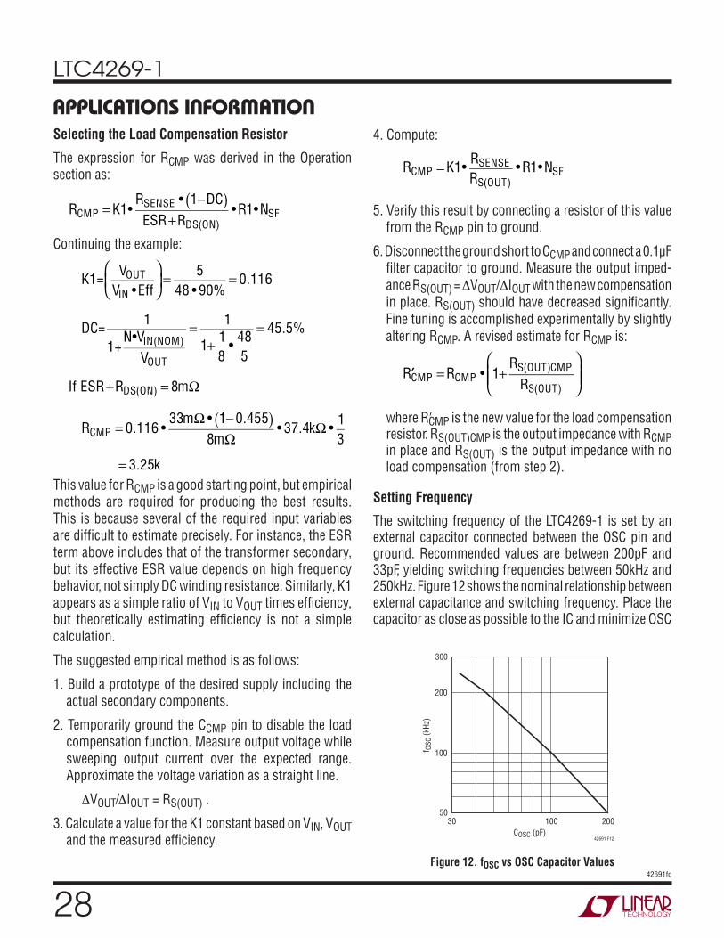
LTC4269-1
2842691fc
APPLICATIONS INFORMATIONSelecting the Load Compensation Resistor
The expression for RCMP was derived in the Operation section as:
RCMP = K1•RSENSE • 1−DC( )
ESR+RDS(ON)
•R1•NSF
Continuing the example:
K1=VOUT
VIN •Eff
⎛
⎝⎜
⎞
⎠⎟ = 5
48 • 90%= 0.116
DC=1
1+N•VIN(NOM)
VOUT
= 1
1+ 1
8•
48
5
= 45.5%
If ESR+RDS(ON) = 8mΩ
RCMP = 0.116 •33mΩ • 1− 0.455( )
8mΩ• 37.4kΩ •
1
3
= 3.25k
This value for RCMP is a good starting point, but empirical methods are required for producing the best results. This is because several of the required input variables are diffi cult to estimate precisely. For instance, the ESR term above includes that of the transformer secondary, but its effective ESR value depends on high frequency behavior, not simply DC winding resistance. Similarly, K1 appears as a simple ratio of VIN to VOUT times effi ciency, but theoretically estimating effi ciency is not a simple calculation.
The suggested empirical method is as follows:
1. Build a prototype of the desired supply including the actual secondary components.
2. Temporarily ground the CCMP pin to disable the load compensation function. Measure output voltage while sweeping output current over the expected range. Approximate the voltage variation as a straight line.
ΔVOUT/ΔIOUT = RS(OUT) .
3. Calculate a value for the K1 constant based on VIN, VOUT and the measured effi ciency.
4. Compute:
RCMP = K1•RSENSE
RS(OUT)
•R1•NSF
5. Verify this result by connecting a resistor of this value from the RCMP pin to ground.
6. Disconnect the ground short to CCMP and connect a 0.1μF fi lter capacitor to ground. Measure the output imped-
ance RS(OUT) = ΔVOUT/ΔIOUT with the new compensation
in place. RS(OUT) should have decreased signifi cantly.
Fine tuning is accomplished experimentally by slightly
altering RCMP. A revised estimate for RCMP is:
′RCMP = RCMP • 1+RS(OUT)CMP
RS(OUT)
⎛
⎝⎜⎜
⎞
⎠⎟⎟
where RCMP is the new value for the load compensation resistor. RS(OUT)CMP is the output impedance with RCMP in place and RS(OUT) is the output impedance with no load compensation (from step 2).
Setting Frequency
The switching frequency of the LTC4269-1 is set by an external capacitor connected between the OSC pin and ground. Recommended values are between 200pF and 33pF, yielding switching frequencies between 50kHz and 250kHz. Figure 12 shows the nominal relationship between external capacitance and switching frequency. Place the capacitor as close as possible to the IC and minimize OSC
COSC (pF)
3050
f OS
C (
kHz)
100
200
300
100 200
42691 F12
Figure 12. fOSC vs OSC Capacitor Values
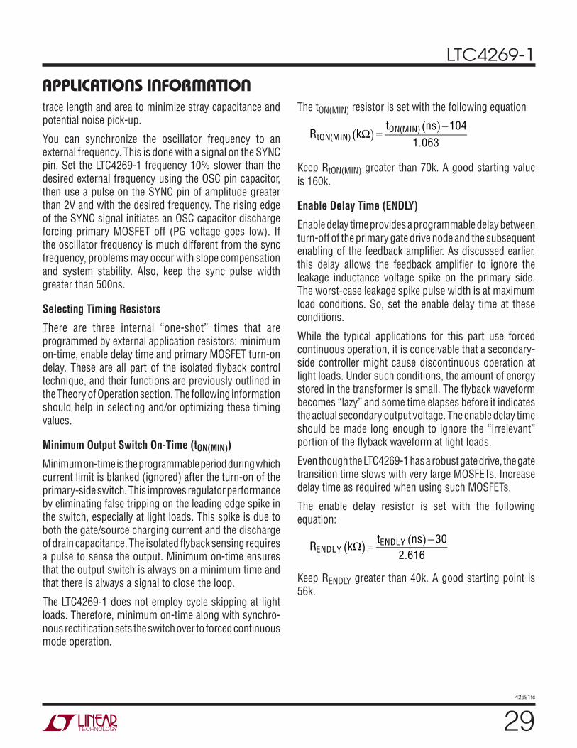
LTC4269-1
2942691fc
APPLICATIONS INFORMATIONtrace length and area to minimize stray capacitance and potential noise pick-up.
You can synchronize the oscillator frequency to an external frequency. This is done with a signal on the SYNC pin. Set the LTC4269-1 frequency 10% slower than the desired external frequency using the OSC pin capacitor, then use a pulse on the SYNC pin of amplitude greater than 2V and with the desired frequency. The rising edge of the SYNC signal initiates an OSC capacitor discharge forcing primary MOSFET off (PG voltage goes low). If the oscillator frequency is much different from the sync frequency, problems may occur with slope compensation and system stability. Also, keep the sync pulse width greater than 500ns.
Selecting Timing Resistors
There are three internal “one-shot” times that are programmed by external application resistors: minimum on-time, enable delay time and primary MOSFET turn-on delay. These are all part of the isolated fl yback control technique, and their functions are previously outlined in the Theory of Operation section. The following information should help in selecting and/or optimizing these timing values.
Minimum Output Switch On-Time (tON(MIN))
Minimum on-time is the programmable period during which current limit is blanked (ignored) after the turn-on of the primary-side switch. This improves regulator performance by eliminating false tripping on the leading edge spike in the switch, especially at light loads. This spike is due to both the gate/source charging current and the discharge of drain capacitance. The isolated fl yback sensing requires a pulse to sense the output. Minimum on-time ensures that the output switch is always on a minimum time and that there is always a signal to close the loop.
The LTC4269-1 does not employ cycle skipping at light loads. Therefore, minimum on-time along with synchro-nous rectifi cation sets the switch over to forced continuous mode operation.
The tON(MIN) resistor is set with the following equation
RtON(MIN) kΩ( ) =
tON(MIN) ns( ) −104
1.063
Keep RtON(MIN) greater than 70k. A good starting value
is 160k.
Enable Delay Time (ENDLY)
Enable delay time provides a programmable delay between turn-off of the primary gate drive node and the subsequent enabling of the feedback amplifi er. As discussed earlier, this delay allows the feedback amplifi er to ignore the leakage inductance voltage spike on the primary side. The worst-case leakage spike pulse width is at maximum load conditions. So, set the enable delay time at these conditions.
While the typical applications for this part use forced continuous operation, it is conceivable that a secondary-side controller might cause discontinuous operation at light loads. Under such conditions, the amount of energy stored in the transformer is small. The fl yback waveform becomes “lazy” and some time elapses before it indicates the actual secondary output voltage. The enable delay time should be made long enough to ignore the “irrelevant” portion of the fl yback waveform at light loads.
Even though the LTC4269-1 has a robust gate drive, the gate transition time slows with very large MOSFETs. Increase delay time as required when using such MOSFETs.
The enable delay resistor is set with the following equation:
RENDLY kΩ( ) = tENDLY ns( ) − 30
2.616
Keep RENDLY greater than 40k. A good starting point is 56k.
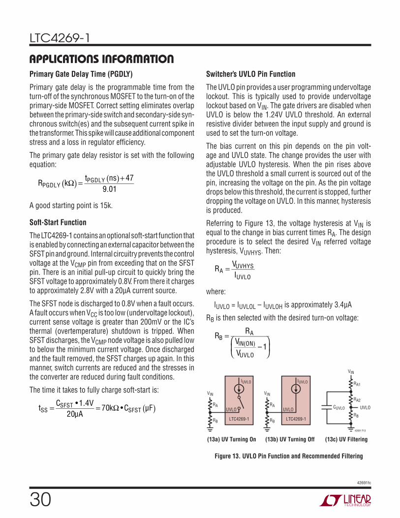
LTC4269-1
3042691fc
Primary Gate Delay Time (PGDLY)
Primary gate delay is the programmable time from the turn-off of the synchronous MOSFET to the turn-on of the primary-side MOSFET. Correct setting eliminates overlap between the primary-side switch and secondary-side syn-chronous switch(es) and the subsequent current spike in the transformer. This spike will cause additional component stress and a loss in regulator effi ciency.
The primary gate delay resistor is set with the following equation:
RPGDLY kΩ( ) = tPGDLY ns( )+ 47
9.01
A good starting point is 15k.
Soft-Start Function
The LTC4269-1 contains an optional soft-start function that is enabled by connecting an external capacitor between the SFST pin and ground. Internal circuitry prevents the control voltage at the VCMP pin from exceeding that on the SFST pin. There is an initial pull-up circuit to quickly bring the SFST voltage to approximately 0.8V. From there it charges to approximately 2.8V with a 20μA current source.
The SFST node is discharged to 0.8V when a fault occurs. A fault occurs when VCC is too low (undervoltage lockout), current sense voltage is greater than 200mV or the IC’s thermal (overtemperature) shutdown is tripped. When SFST discharges, the VCMP node voltage is also pulled low to below the minimum current voltage. Once discharged and the fault removed, the SFST charges up again. In this manner, switch currents are reduced and the stresses in the converter are reduced during fault conditions.
The time it takes to fully charge soft-start is:
tSS = CSFST • 1.4V
20μA= 70kΩ • CSFST μF( )
Switcher’s UVLO Pin Function
The UVLO pin provides a user programming undervoltage lockout. This is typically used to provide undervoltage lockout based on VIN. The gate drivers are disabled when UVLO is below the 1.24V UVLO threshold. An external resistive divider between the input supply and ground is used to set the turn-on voltage.
The bias current on this pin depends on the pin volt-age and UVLO state. The change provides the user with adjustable UVLO hysteresis. When the pin rises above the UVLO threshold a small current is sourced out of the pin, increasing the voltage on the pin. As the pin voltage drops below this threshold, the current is stopped, further dropping the voltage on UVLO. In this manner, hysteresis is produced.
Referring to Figure 13, the voltage hysteresis at VIN is equal to the change in bias current times RA. The design procedure is to select the desired VIN referred voltage hysteresis, VUVHYS. Then:
RA = VUVHYS
IUVLO
where:
IUVLO = IUVLOL – IUVLOH is approximately 3.4μA
RB is then selected with the desired turn-on voltage:
RB = RA
VIN(ON)
VUVLO
– 1⎛
⎝⎜
⎞
⎠⎟
APPLICATIONS INFORMATION
VIN
RA
LTC4269-1
(13a) UV Turning On
UVLO
IUVLO
RB
VIN
RA
LTC4269-1
(13b) UV Turning Off (13c) UV Filtering
UVLO UVLO
RB
VIN
RA2
RA1
CUVLO
RB
42691 F13
IUVLO
Figure 13. UVLO Pin Function and Recommended Filtering
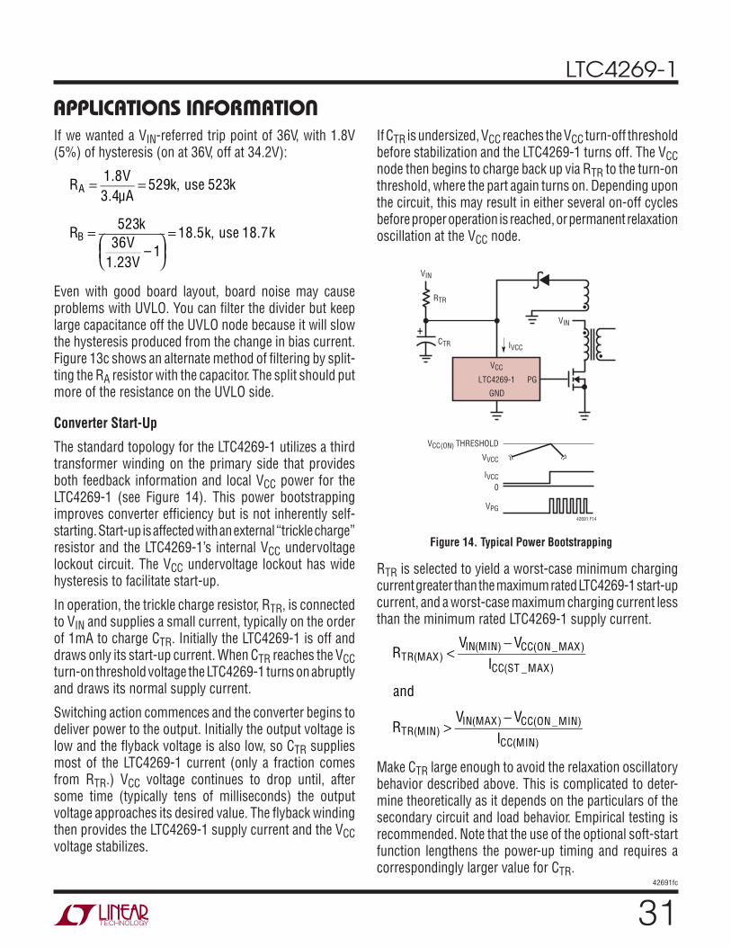
LTC4269-1
3142691fc
APPLICATIONS INFORMATIONIf we wanted a VIN-referred trip point of 36V, with 1.8V (5%) of hysteresis (on at 36V, off at 34.2V):
RA = 1.8V
3.4μA= 529k, use 523k
RB = 523k
36V
1.23V– 1
⎛⎝⎜
⎞⎠⎟
= 18.5k, use 18.7k
Even with good board layout, board noise may cause problems with UVLO. You can fi lter the divider but keep large capacitance off the UVLO node because it will slow the hysteresis produced from the change in bias current. Figure 13c shows an alternate method of fi ltering by split-ting the RA resistor with the capacitor. The split should put more of the resistance on the UVLO side.
Converter Start-Up
The standard topology for the LTC4269-1 utilizes a third transformer winding on the primary side that provides both feedback information and local VCC power for the LTC4269-1 (see Figure 14). This power bootstrapping improves converter effi ciency but is not inherently self-starting. Start-up is affected with an external “trickle charge” resistor and the LTC4269-1’s internal VCC undervoltage lockout circuit. The VCC undervoltage lockout has wide hysteresis to facilitate start-up.
In operation, the trickle charge resistor, RTR, is connected to VIN and supplies a small current, typically on the order of 1mA to charge CTR. Initially the LTC4269-1 is off and draws only its start-up current. When CTR reaches the VCC turn-on threshold voltage the LTC4269-1 turns on abruptly and draws its normal supply current.
Switching action commences and the converter begins to deliver power to the output. Initially the output voltage is low and the fl yback voltage is also low, so CTR supplies most of the LTC4269-1 current (only a fraction comes from RTR.) VCC voltage continues to drop until, after some time (typically tens of milliseconds) the output voltage approaches its desired value. The fl yback winding then provides the LTC4269-1 supply current and the VCC voltage stabilizes.
If CTR is undersized, VCC reaches the VCC turn-off threshold before stabilization and the LTC4269-1 turns off. The VCC node then begins to charge back up via RTR to the turn-on threshold, where the part again turns on. Depending upon the circuit, this may result in either several on-off cycles before proper operation is reached, or permanent relaxation oscillation at the VCC node.
RTR is selected to yield a worst-case minimum charging current greater than the maximum rated LTC4269-1 start-up current, and a worst-case maximum charging current less than the minimum rated LTC4269-1 supply current.
RTR(MAX) <VIN(MIN) − VCC(ON _MAX)
ICC(ST _MAX)
and
RTR(MIN) >VIN(MAX) − VCC(ON _MIN)
ICC(MIN)
Make CTR large enough to avoid the relaxation oscillatory behavior described above. This is complicated to deter-mine theoretically as it depends on the particulars of the secondary circuit and load behavior. Empirical testing is recommended. Note that the use of the optional soft-start function lengthens the power-up timing and requires a correspondingly larger value for CTR.
+IVCC
42691 F14
RTR
CTR
VIN
VIN
IVCC
VVCC
VCC(ON) THRESHOLD
0
VPG
VCC
LTC4269-1 PG
GND
•
•
•
Figure 14. Typical Power Bootstrapping
LTC4269-1
3242691fc
The LTC4269-1 has an internal clamp on VCC of approxi-mately 19.5V. This provides some protection for the part in the event that the switcher is off (UVLO low) and the VCC node is pulled high. If RTR is sized correctly, the part should never attain this clamp voltage.
Control Loop Compensation
Loop frequency compensation is performed by connect-ing a capacitor network from the output of the feedback amplifi er (VCMP pin) to ground as shown in Figure 15. Because of the sampling behavior of the feedback amplifi er, compensation is different from traditional current mode controllers. Normally only CVCMP is required. RVCMP can be used to add a zero, but the phase margin improvement traditionally offered by this extra resistor is usually already accomplished by the nonzero secondary circuit impedance. CVCMP2 can be used to add an additional high frequency pole and is usually sized at 0.1 times CVCMP.
Slope Compensation
The LTC4269-1 incorporates current slope compensation. Slope compensation is required to ensure current loop stability when the DC is greater than 50%. In some switching regulators, slope compensation reduces the maximum peak current at higher duty cycles. The LTC4269-1 eliminates this problem by having circuitry that compensates for the slope compensation so that maximum current sense voltage is constant across all duty cycles.
Minimum Load Considerations
At light loads, the LTC4269-1 derived regulator goes into forced continuous conduction mode. The primary-side switch always turns on for a short time as set by the tON(MIN) resistor. If this produces more power than the load requires, power will fl ow back into the primary dur-ing the off period when the synchronization switch is on. This does not produce any inherently adverse problems, although light load effi ciency is reduced.
Maximum Load Considerations
The current mode control uses the VCMP node voltage and amplifi ed sense resistor voltage as inputs to the current comparator. When the amplifi ed sense voltage exceeds the VCMP node voltage, the primary-side switch is turned off.
In normal use, the peak switch current increases while FB is below the internal reference. This continues until VCMP reaches its 2.56V clamp. At clamp, the primary-side MOSFET will turn off at the rated 100mV VSENSE level. This repeats on the next cycle.
It is possible for the peak primary switch currents as referred across RSENSE to exceed the max 100mV rating because of the minimum switch on time blanking. If the voltage on VSENSE exceeds 205mV after the minimum turn-on time, the SFST capacitor is discharged, causing the discharge of the VCMP capacitor. This then reduces the peak current on the next cycle and will reduce overall stress in the primary switch.
APPLICATIONS INFORMATION
17
RVCMP
VCMP
CVCMP
42691 F15
CVCMP2
Figure 15. VCMP Compensation Network
In further contrast to traditional current mode switchers, VCMP pin ripple is generally not an issue with the LTC4269-1. The dynamic nature of the clamped feedback amplifi er forms an effective track/hold type response, whereby the VCMP voltage changes during the fl yback pulse, but is then held during the subsequent switch-on portion of the next cycle. This action naturally holds the VCMP voltage stable during the current comparator sense action (current mode switching).
Application Note 19 provides a method for empirically tweaking frequency compensation. Basically, it involves introducing a load current step and monitoring the response.
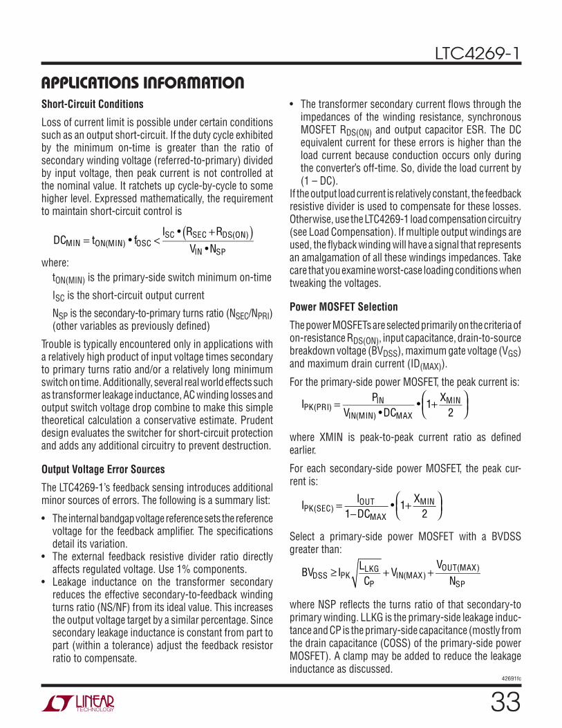
LTC4269-1
3342691fc
Short-Circuit Conditions
Loss of current limit is possible under certain conditions such as an output short-circuit. If the duty cycle exhibited by the minimum on-time is greater than the ratio of secondary winding voltage (referred-to-primary) divided by input voltage, then peak current is not controlled at the nominal value. It ratchets up cycle-by-cycle to some higher level. Expressed mathematically, the requirement to maintain short-circuit control is
DCMIN = tON(MIN) • fOSC <ISC • RSEC +RDS(ON)( )
VIN •NSP
where:
tON(MIN) is the primary-side switch minimum on-time
ISC is the short-circuit output current
NSP is the secondary-to-primary turns ratio (NSEC/NPRI) (other variables as previously defi ned)
Trouble is typically encountered only in applications with a relatively high product of input voltage times secondary to primary turns ratio and/or a relatively long minimum switch on time. Additionally, several real world effects such as transformer leakage inductance, AC winding losses and output switch voltage drop combine to make this simple theoretical calculation a conservative estimate. Prudent design evaluates the switcher for short-circuit protection and adds any additional circuitry to prevent destruction.
Output Voltage Error Sources
The LTC4269-1’s feedback sensing introduces additional minor sources of errors. The following is a summary list:
• The internal bandgap voltage reference sets the reference voltage for the feedback amplifi er. The specifi cations detail its variation.
• The external feedback resistive divider ratio directly affects regulated voltage. Use 1% components.
• Leakage inductance on the transformer secondary reduces the effective secondary-to-feedback winding turns ratio (NS/NF) from its ideal value. This increases the output voltage target by a similar percentage. Since secondary leakage inductance is constant from part to part (within a tolerance) adjust the feedback resistor ratio to compensate.
APPLICATIONS INFORMATION• The transformer secondary current fl ows through the
impedances of the winding resistance, synchronous MOSFET RDS(ON) and output capacitor ESR. The DC equivalent current for these errors is higher than the load current because conduction occurs only during the converter’s off-time. So, divide the load current by (1 – DC).
If the output load current is relatively constant, the feedback resistive divider is used to compensate for these losses. Otherwise, use the LTC4269-1 load compensation circuitry (see Load Compensation). If multiple output windings are used, the fl yback winding will have a signal that represents an amalgamation of all these windings impedances. Take care that you examine worst-case loading conditions when tweaking the voltages.
Power MOSFET Selection
The power MOSFETs are selected primarily on the criteria of on-resistance RDS(ON), input capacitance, drain-to-source breakdown voltage (BVDSS), maximum gate voltage (VGS) and maximum drain current (ID(MAX)).
For the primary-side power MOSFET, the peak current is:
IPK(PRI) = PIN
VIN(MIN) •DCMAX
• 1+ XMIN
2
⎛⎝⎜
⎞⎠⎟
where XMIN is peak-to-peak current ratio as defi ned earlier.
For each secondary-side power MOSFET, the peak cur-rent is:
IPK(SEC) = IOUT
1−DCMAX
• 1+ XMIN
2
⎛⎝⎜
⎞⎠⎟
Select a primary-side power MOSFET with a BVDSS greater than:
BVDSS ≥ IPKLLKG
CP
+ VIN(MAX) +VOUT(MAX)
NSP
where NSP refl ects the turns ratio of that secondary-to primary winding. LLKG is the primary-side leakage induc-tance and CP is the primary-side capacitance (mostly from the drain capacitance (COSS) of the primary-side power MOSFET). A clamp may be added to reduce the leakage inductance as discussed.
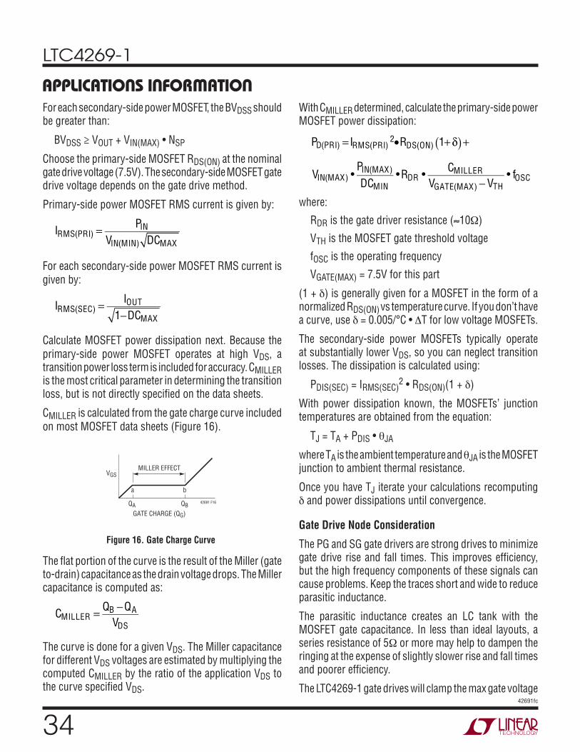
LTC4269-1
3442691fc
APPLICATIONS INFORMATIONFor each secondary-side power MOSFET, the BVDSS should be greater than:
BVDSS ≥ VOUT + VIN(MAX) • NSP
Choose the primary-side MOSFET RDS(ON) at the nominal gate drive voltage (7.5V). The secondary-side MOSFET gate drive voltage depends on the gate drive method.
Primary-side power MOSFET RMS current is given by:
IRMS(PRI) = PIN
VIN(MIN) DCMAX
For each secondary-side power MOSFET RMS current is
given by:
IRMS(SEC) = IOUT
1−DCMAX
Calculate MOSFET power dissipation next. Because the
primary-side power MOSFET operates at high VDS, a transition power loss term is included for accuracy. CMILLER is the most critical parameter in determining the transition loss, but is not directly specifi ed on the data sheets.
CMILLER is calculated from the gate charge curve included
on most MOSFET data sheets (Figure 16).
With CMILLER determined, calculate the primary-side power MOSFET power dissipation:
PD(PRI) = IRMS(PRI)2•RDS(ON) 1+ δ( )+
VIN(MAX) •PIN(MAX)
DCMIN
•RDR •CMILLER
VGATE(MAX) − VTH
• fOSC
where:
RDR is the gate driver resistance (≈10Ω)
VTH is the MOSFET gate threshold voltage
fOSC is the operating frequency
VGATE(MAX) = 7.5V for this part
(1 + δ) is generally given for a MOSFET in the form of a normalized RDS(ON) vs temperature curve. If you don’t have a curve, use δ = 0.005/°C • ΔT for low voltage MOSFETs.
The secondary-side power MOSFETs typically operate at substantially lower VDS, so you can neglect transition losses. The dissipation is calculated using:
PDIS(SEC) = IRMS(SEC)2 • RDS(ON)(1 + δ)
With power dissipation known, the MOSFETs’ junction temperatures are obtained from the equation:
TJ = TA + PDIS • θJA
where TA is the ambient temperature and θJA is the MOSFET junction to ambient thermal resistance.
Once you have TJ iterate your calculations recomputing δ and power dissipations until convergence.
Gate Drive Node Consideration
The PG and SG gate drivers are strong drives to minimize gate drive rise and fall times. This improves effi ciency, but the high frequency components of these signals can cause problems. Keep the traces short and wide to reduce parasitic inductance.
The parasitic inductance creates an LC tank with the MOSFET gate capacitance. In less than ideal layouts, a series resistance of 5Ω or more may help to dampen the ringing at the expense of slightly slower rise and fall times and poorer effi ciency.
The LTC4269-1 gate drives will clamp the max gate voltage
QA
VGS
a b
42691 F16QB
MILLER EFFECT
GATE CHARGE (QG)
Figure 16. Gate Charge Curve
The fl at portion of the curve is the result of the Miller (gate to-drain) capacitance as the drain voltage drops. The Miller capacitance is computed as:
CMILLER = QB −QA
VDS
The curve is done for a given VDS. The Miller capacitance for different VDS voltages are estimated by multiplying the computed CMILLER by the ratio of the application VDS to the curve specifi ed VDS.
LTC4269-1
3542691fc
APPLICATIONS INFORMATIONto roughly 7.5V, so you can safely use MOSFETs with maximum VGS of 10V and larger.
Synchronous Gate Drive
There are several different ways to drive the synchronous gate MOSFET. Full converter isolation requires the synchro-nous gate drive to be isolated. This is usually accomplished by way of a pulse transformer. Usually the pulse driver is used to drive a buffer on the secondary, as shown in the application on the front page of this data sheet.
However, other schemes are possible. There are gate drivers and secondary-side synchronous controllers available that provide the buffer function as well as additional features.
Capacitor Selection
In a fl yback converter, the input and output current fl ows in pulses, placing severe demands on the input and output fi lter capacitors. The input and output fi lter capacitors are selected based on RMS current ratings and ripple voltage.
Select an input capacitor with a ripple current rating greater than:
IRMS(PRI) = PIN
VIN(MIN)
1−DCMAX
DCMAX
Continuing the example:
IRMS(PRI) = 29.5W
41V
1− 49.4%
49.4%= 0.728A
Keep input capacitor series resistance (ESR) and inductance (ESL) small, as they affect electromagnetic interference suppression. In some instances, high ESR can also produce stability problems because fl yback converters exhibit a negative input resistance characteristic. Refer to Application Note 19 for more information.
The output capacitor is sized to handle the ripple current and to ensure acceptable output voltage ripple. The output capacitor should have an RMS current rating greater than:
IRMS(SEC) = IOUTDCMAX
1−DCMAX
Continuing the example:
IRMS(SEC) = 5.3A49.4%
1− 49.4%= 5.24A
This is calculated for each output in a multiple winding application.
ESR and ESL along with bulk capacitance directly affect the output voltage ripple. The waveforms for a typical fl yback converter are illustrated in Figure 17.
The maximum acceptable ripple voltage (expressed as a percentage of the output voltage) is used to establish a starting point for the capacitor values. For the purpose of simplicity, we will choose 2% for the maximum output
OUTPUT VOLTAGERIPPLE WAVEFORM
SECONDARYCURRENT
PRIMARYCURRENT
IPRI
ΔVCOUT
42691 F17
RINGINGDUE TO ESL
IPRI
N
ΔVESR
Figure 17. Typical Flyback Converter Waveforms
ripple, divided equally between the ESR step and the charging/discharging ΔV. This percentage ripple changes, depending on the requirements of the application. You can modify the following equations.
For a 1% contribution to the total ripple voltage, the ESR
of the output capacitor is determined by:
ESRCOUT ≤ 1% •VOUT • 1−DCMAX( )
IOUT
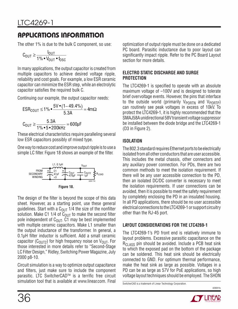
LTC4269-1
3642691fc
The other 1% is due to the bulk C component, so use:
COUT ≥ IOUT
1% • VOUT • fOSC
In many applications, the output capacitor is created from multiple capacitors to achieve desired voltage ripple, reliability and cost goals. For example, a low ESR ceramic capacitor can minimize the ESR step, while an electrolytic capacitor satisfi es the required bulk C.
Continuing our example, the output capacitor needs:
ESRCOUT ≤ 1% •5V • 1− 49.4%( )
5.3A= 4mΩ
COUT ≥ 5.3A
1% • 5 • 200kHz= 600μF
These electrical characteristics require paralleling several low ESR capacitors possibly of mixed type.
One way to reduce cost and improve output ripple is to use a simple LC fi lter. Figure 18 shows an example of the fi lter.
APPLICATIONS INFORMATIONoptimization of output ripple must be done on a dedicated PC board. Parasitic inductance due to poor layout can signifi cantly impact ripple. Refer to the PC Board Layout section for more details.
ELECTRO STATIC DISCHARGE AND SURGE PROTECTION
The LTC4269-1 is specifi ed to operate with an absolute maximum voltage of –100V and is designed to tolerate brief overvoltage events. However, the pins that interface to the outside world (primarily VPORTN and VPORTP) can routinely see peak voltages in excess of 10kV. To protect the LTC4269-1, it is highly recommended that the SMAJ58A unidirectional 58V transient voltage suppressor be installed between the diode bridge and the LTC4269-1 (D3 in Figure 2).
ISOLATION
The 802.3 standard requires Ethernet ports to be electrically isolated from all other conductors that are user accessible. This includes the metal chassis, other connectors and any auxiliary power connection. For PDs, there are two common methods to meet the isolation requirement. If there will be any user accessible connection to the PD, then an isolated DC/DC converter is necessary to meet the isolation requirements. If user connections can be avoided, then it is possible to meet the safety requirement by completely enclosing the PD in an insulated housing. In all PD applications, there should be no user accessible electrical connections to the LTC4269-1 or support circuitry other than the RJ-45 port.
LAYOUT CONSIDERATIONS FOR THE LTC4269-1
The LTC4269-1’s PD front end is relatively immune to layout problems. Excessive parasitic capacitance on the RCLASS pin should be avoided. Include a PCB heat sink to which the exposed pad on the bottom of the package can be soldered. This heat sink should be electrically connected to GND. For optimum thermal performance, make the heat sink as large as possible. Voltages in a PD can be as large as 57V for PoE applications, so high voltage layout techniques should be employed. The SHDN
RLOADCOUT21μF
VOUT
COUT470μF
C147μF
3
FROMSECONDARY
WINDING
L1, 0.1μH
42691 F18
++
Figure 18.
The design of the fi lter is beyond the scope of this data sheet. However, as a starting point, use these general guidelines. Start with a COUT 1/4 the size of the nonfi lter solution. Make C1 1/4 of COUT to make the second fi lter pole independent of COUT. C1 may be best implemented with multiple ceramic capacitors. Make L1 smaller than the output inductance of the transformer. In general, a 0.1μH fi lter inductor is suffi cient. Add a small ceramic capacitor (COUT2) for high frequency noise on VOUT. For those interested in more details refer to “Second-Stage LC Filter Design,” Ridley, Switching Power Magazine, July 2000 p8-10.
Circuit simulation is a way to optimize output capacitance and fi lters, just make sure to include the component parasitic. LTC SwitcherCADTM is a terrifi c free circuit simulation tool that is available at www.linear.com. Final
SwitcherCAD is a trademark of Linear Technology Corporation.
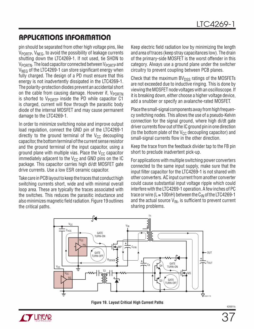
LTC4269-1
3742691fc
pin should be separated from other high voltage pins, like VPORTP, VNEG, to avoid the possibility of leakage currents shutting down the LTC4269-1. If not used, tie SHDN to VPORTN. The load capacitor connected between VPORTP and VNEG of the LTC4269-1 can store signifi cant energy when fully charged. The design of a PD must ensure that this energy is not inadvertently dissipated in the LTC4269-1. The polarity-protection diodes prevent an accidental short on the cable from causing damage. However if, VPORTN is shorted to VPORTP inside the PD while capacitor C1 is charged, current will fl ow through the parasitic body diode of the internal MOSFET and may cause permanent damage to the LTC4269-1.
In order to minimize switching noise and improve output load regulation, connect the GND pin of the LTC4269-1 directly to the ground terminal of the VCC decoupling capacitor, the bottom terminal of the current sense resistor and the ground terminal of the input capacitor, using a ground plane with multiple vias. Place the VCC capacitor immediately adjacent to the VCC and GND pins on the IC package. This capacitor carries high di/dt MOSFET gate drive currents. Use a low ESR ceramic capacitor.
Take care in PCB layout to keep the traces that conduct high switching currents short, wide and with minimal overall loop area. These are typically the traces associated with the switches. This reduces the parasitic inductance and also minimizes magnetic fi eld radiation. Figure 19 outlines the critical paths.
Keep electric fi eld radiation low by minimizing the length and area of traces (keep stray capacitances low). The drain of the primary-side MOSFET is the worst offender in this category. Always use a ground plane under the switcher circuitry to prevent coupling between PCB planes.
Check that the maximum BVDSS ratings of the MOSFETs are not exceeded due to inductive ringing. This is done by viewing the MOSFET node voltages with an oscilloscope. If it is breaking down, either choose a higher voltage device, add a snubber or specify an avalanche-rated MOSFET.
Place the small-signal components away from high frequen-cy switching nodes. This allows the use of a pseudo-Kelvin connection for the signal ground, where high di/dt gate driver currents fl ow out of the IC ground pin in one direction (to the bottom plate of the VCC decoupling capacitor) and small-signal currents fl ow in the other direction.
Keep the trace from the feedback divider tap to the FB pin short to preclude inadvertent pick-up.
For applications with multiple switching power converters connected to the same input supply, make sure that the input fi lter capacitor for the LTC4269-1 is not shared with other converters. AC input current from another converter could cause substantial input voltage ripple which could interfere with the LTC4269-1 operation. A few inches of PC trace or wire (L ≅ 100nH) between the CIN of the LTC4269-1 and the actual source VIN, is suffi cient to prevent current sharing problems.
APPLICATIONS INFORMATION
T2
T1
CR
CVIN
MS
MP
GATETURN-ON
GATETURN-ON
RSENSE
• •
CVCC
SG
VCC
PG
VCC
VCC
VCC
VIN
GATETURN-OFF
GATETURN-OFF
Q4
Q3
COUT
42691 F19
OUT
•
•
•+
++
Figure 19. Layout Critical High Current Paths
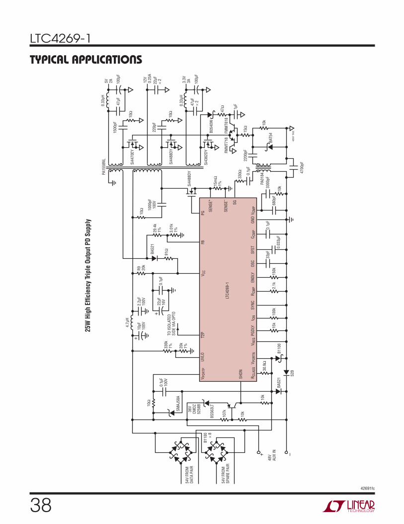
LTC4269-1
3842691fc
TYPICAL APPLICATIONS
25W
Hig
h Ef
fi cie
ncy
Trip
le O
utpu
t P
D S
uppl
y
10
0k
30
.9Ω
91
Ω
3.0
1k
1%
29
.4k
1%
22
μF
16
V
R9
20
k
0.1
μF
BA
S2
1
2.1
k1
50
k
33
pF
10
μF
10
0V
TO
IS
OL
AT
ED
SID
E V
IA O
PT
O
0.1
μF
10
0V
SM
AJ5
8A
2.2
μF
10
0V
0.1
μF
t ON
15
k
PG
DLY
VN
EG
S2
B
B1
10
00
.03
3μ
F
SY
NC
RC
LA
SS
SH
DN
VC
MP
RC
MP
EN
DLY
OS
CS
FST
LTC
42
69
-1
GN
D
UV
LO
VP
OR
TP
VC
CFB
CC
MP
T2
P
4.7
μH
BS
S6
3LT
+
+
VP
OR
TN
10
7k
10
Ω
10
k
10
k
54V
FR
OM
DA
TA
PA
IR
54V
FR
OM
SP
AR
E P
AIR
B1
10
0×
8
36
VC
MD
Z5
25
8B
33
0k
1%
20
k1
%
10
k
68
0p
F
33
00pF
48V
AUX
IN
15m
Ω1%
Si4
488D
Y
Si4
362D
Y
10k
15Ω
47Ω
10Ω
10
Ω
B0540W
PA
0184
BA
T54
330Ω
2200pF
4700pF
FMM
T718
FMM
T618
220pF
0.1
μF
1μF47μF
× 2
100μF
3.3
V3A
0.3
3μH
PA
1558N
L
42
69
1 T
A0
2
SE
NS
E–
SE
NS
E+
SG
PG
0.3
3μH
10
00
pF
10
0V
100μF
Si4
488D
Y
12V
0.2
5A
22μF
× 2
10Ω
1500pF
Si4
470EY
47μF
5V
2A
+
+ –
+
BA
S2
1
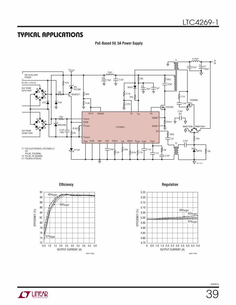
LTC4269-1
3942691fc
TYPICAL APPLICATIONSPoE-Based 5V, 5A Power Supply
100k
150Ω
30.9Ω
20Ω
3.01k
27.4k
39k
BAS21
1.2k38.3k
33pF
0.1μF100V
10μF
VPORTP
0.1μF
tON
12k
PGDLYVNEG
S1B
B1100
S1B
SYNC
RCLASS
SHDN
VCMPRCMPENDLYOSC
LTC4269-1
GND
UVLO
VPORTP
VCCFB
CCMP
10μH
BSS63LT1
36VPDZ36B
SMAJ58A
+
VPORTN
107k
24k
10k
10Ω
54V FROMSPARE PAIR
T1: PCA ELECTRONICS, EPC3409G-LF OR PULSE, PA2369NLT2: PULSE, PE-68386NLC1: PSLB20J107M(45)
54V FROMDATA PAIR
48V AUXILIARYPOWER
B1100 × 8 PLCS
383k
14.0k
10k
1nF3.3nF
33mΩ
FDS2582
10k
15Ω
BAT54
100Ω
2.2nF
MMBT3906 MMBT3904
T2
FDS8880
1μF
T1
42691 TA03a
SENSE–
SENSE+
SG
PGPWRGD
0.18μH
C1100μF
2.2nF2kV
47μF
5V5A
+
+
–
1μF
22pF
1.5nF
10μF+
2.2μF
5.1Ω
5.04.5
EFF
ICIE
NC
Y (
%)
80
90
92
76
86
78
88
74
72
84
82
OUTPUT CURRENT (A)
42691 TA03b
42VPORT
57VPORT
0.5 1.0 2.0 3.01.5 4.02.5 3.5
50VPORT
Effi ciency Regulation
OUTPUT CURRENT (A)
0
EFF
ICIE
NC
Y (
%)
4.95
5.20
5.25
1.0 2.0 3.0
4.85
5.10
4.90
5.15
4.80
4.75
5.05
5.00
0.5 1.5 4.0 5.02.5 3.5 4.5
42691 TA03c
42VPORT
57VPORT
50VPORT
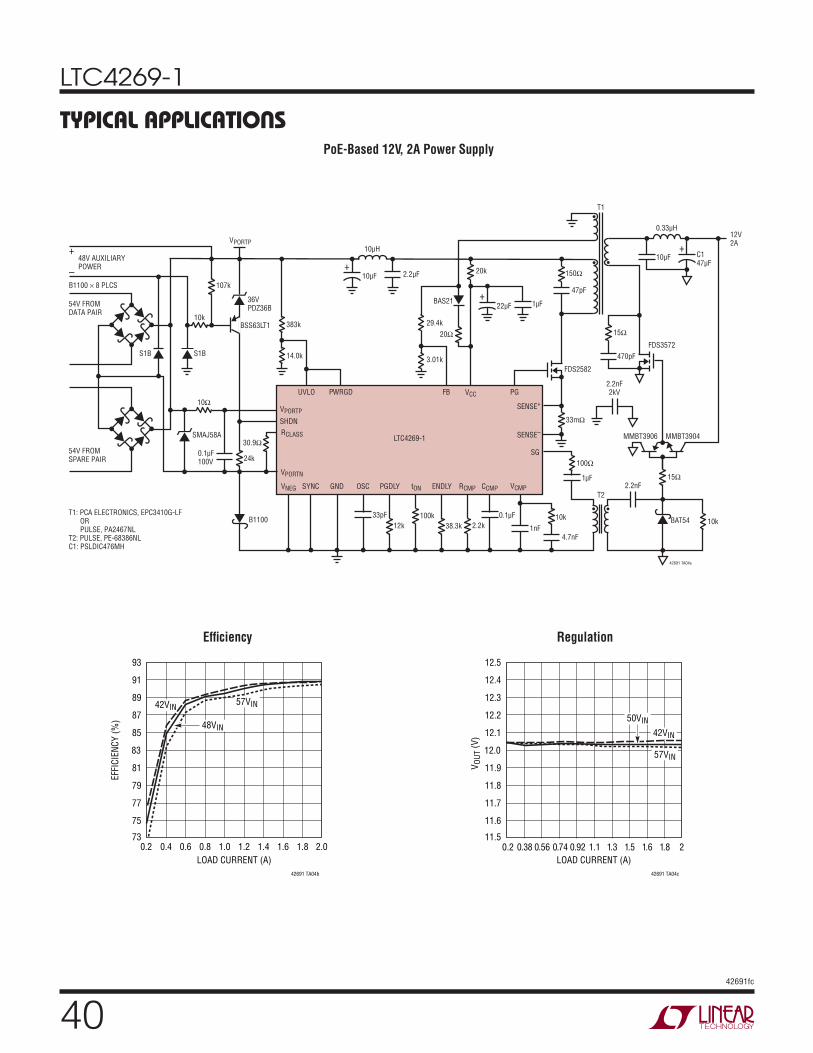
LTC4269-1
4042691fc
TYPICAL APPLICATIONSPoE-Based 12V, 2A Power Supply
100k
150Ω
30.9Ω
20Ω
3.01k
29.4k
20k
BAS21
2.2k38.3k
33pF
0.1μF100V
22μF
VPORTP
0.1μF
tON
12k
PGDLYVNEG
S1BS1B
SYNC
RCLASS
SHDN
VCMPRCMPENDLYOSC
LTC4269-1
GND
UVLO
VPORTP
VCCFB
CCMP
10μH
BSS63LT1
36VPDZ36B
SMAJ58A
+
VPORTN
107k
24k
10k
10Ω
54V FROMSPARE PAIR
54V FROMDATA PAIR
48V AUXILIARYPOWER
B1100 × 8 PLCS
383k
14.0k
10k
1nF4.7nF
33mΩ
FDS2582
10k
15Ω
BAT54B1100
100Ω
2.2nF
MMBT3906 MMBT3904
FDS3572
1μF
42691 TA04a
SENSE–
SENSE+
SG
PG
0.33μH
2.2nF2kV
10μF
12V2A
++
–
1μF
47pF
470pF
10μF+
2.2μF
15Ω
T1: PCA ELECTRONICS, EPC3410G-LF OR PULSE, PA2467NLT2: PULSE, PE-68386NLC1: PSLDIC476MH
T2
T1
C147μF
PWRGD
LOAD CURRENT (A)
0.2
EFF
ICIE
NC
Y (
%)
81
91
93
0.4 0.8 1.2
77
87
79
89
75
73
85
83
0.6 1.6 2.01.0 1.4 1.8
42691 TA04b
42VIN
48VIN
57VIN
LOAD CURRENT (A)
0.2
11.9
12.4
12.5
0.38 0.74 1.1
11.7
12.2
11.8
12.3
11.6
11.5
12.1
12.0
0.56 1.5 20.92 1.3 1.6 1.8
42691 TA04c
42VIN
57VIN
50VIN
VO
UT (
V)
Effi ciency Regulation
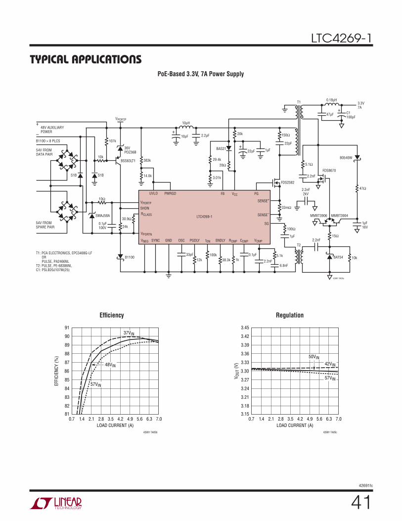
LTC4269-1
4142691fc
TYPICAL APPLICATIONSPoE-Based 3.3V, 7A Power Supply
100k
150Ω
30.9Ω
20Ω
3.01k
29.4k
20k
BAS21
1k38.3k
33pF
0.1μF100V
22μF
VPORTP
0.1μF
tON
12k
PGDLYVNEG
S1BS1B
SYNC
RCLASS
SHDN
VCMPRCMPENDLYOSC
LTC4269-1
GND
UVLO
VPORTP
VCCFB
CCMP
10μH
BSS63LT1
36VPDZ36B
SMAJ58A
+
VPORTN
107k
24k
10k
10Ω
54V FROMSPARE PAIR
54V FROMDATA PAIR
48V AUXILIARYPOWER
B1100 × 8 PLCS
383k
14.0k
5.1k
2.2nF6.8nF
33mΩ
FDS2582
10k
15Ω
BAT54
100Ω
2.2nF
MMBT3906 MMBT3904
FDS8670
1μF
1μF16V
42691 TA05a
SENSE–
SENSE+
SG
PG
0.18μH
2.2nF2kV
47μF
3.3V7A
+
+
–
B1100
B0540W
1μF
22pF
2.2nF
10μF+
2.2μF
5.1Ω
47Ω
T1: PCA ELECTRONICS, EPC3408G-LF OR PULSE, PA2466NLT2: PULSE, PE-68386NLC1: PSLB20J107M(25)
T2
T1
C1100μF
PWRGD
Effi ciency Regulation
LOAD CURRENT (A)
0.7
EFF
ICIE
NC
Y (
%)
85
90
91
1.4 2.8 4.2
83
88
84
89
82
81
87
86
2.1 5.6 7.03.5 4.9 6.3
42691 TA05b
37VIN
48VIN
57VIN
LOAD CURRENT (A)
3.27
3.42
3.45
3.21
3.36
3.24
3.39
3.18
3.15
3.33
3.30
42691 TA05c
42VIN
50VIN
57VINVO
UT (
V)
0.7 1.4 2.8 4.22.1 5.6 7.03.5 4.9 6.3
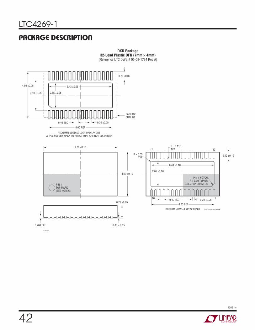
LTC4269-1
4242691fc
PACKAGE DESCRIPTION
NOTE:
PIN 1TOP MARK(SEE NOTE 6)
BOTTOM VIEW—EXPOSED PAD
R = 0.115TYP
0.20 ±0.05116
17 32
6.00 REF
6.43 ±0.10
2.65 ±0.104.00 ±0.10
0.75 ±0.05
0.00 – 0.050.200 REF
7.00 ±0.10
(DKD32) QFN 0707 REV A
0.40 BSC
RECOMMENDED SOLDER PAD LAYOUTAPPLY SOLDER MASK TO AREAS THAT ARE NOT SOLDERED
PIN 1 NOTCHR = 0.30 TYP OR
0.35 45° CHAMFER
6.43 ±0.05
2.65 ±0.05
0.70 ±0.05
0.40 BSC
6.00 REF
3.10 ±0.05
4.50 ±0.05
0.40 ±0.10
0.20 ±0.05
PACKAGEOUTLINE
R = 0.05TYP
DKD Package32-Lead Plastic DFN (7mm × 4mm)
(Reference LTC DWG # 05-08-1734 Rev A)
LTC4269-1
4342691fc
Information furnished by Linear Technology Corporation is believed to be accurate and reliable. However, no responsibility is assumed for its use. Linear Technology Corporation makes no representa-tion that the interconnection of its circuits as described herein will not infringe on existing patent rights.
REVISION HISTORYREV DATE DESCRIPTION PAGE NUMBER
B 04/10 Connected PWRGD Pin to UVLO Pin in Typical Application Circuit Drawings
Added Text Clarifying Connecting PWRGD Pin to UVLO Pin in Complementary Power Good Section of the Applications Information Section
1, 39-41
16, 17
C 08/12 Updated maximum power levels for class 0 and class 3 to 13.0W
Added 10Ω resistor to VPORTP pin in Figure 7 and supporting text in Input Series Resistance section
Added SMAJ58A (TVS) recommendation paragraph
Figure 8: Changed connection of photodiode (cathode side) from VNEG to –54V rail
Figure 9: Added Schottky diode between VPORTN and VNEG to make solution more robust to surges
Schematic changes to make solution more robust to surges: added 10Ω resistor to VPORTP pin, added Schottky diode to VPORTN pin, and changed diode going from VPORTN to negative auxiliary input to S1B
14
18, 19
19
19
20
38, 39, 40, 41
(Revision history begins at Rev B)
LTC4269-1
4442691fc
Linear Technology Corporation1630 McCarthy Blvd., Milpitas, CA 95035-7417 (408) 432-1900 ● FAX: (408) 434-0507 ● www.linear.com © LINEAR TECHNOLOGY CORPORATION 2009
LT 0812 REV C • PRINTED IN USA
RELATED PARTSPART NUMBER DESCRIPTION COMMENTS
LTC4257-1 IEEE 802.3af PD Interface Controller 100V 400mA Internal Switch, Programmable Classifi cation, Dual Current Limit
LTC4258 Quad IEEE 802.3af Power over Ethernet Controller DC Disconnect Only, IEEE-Compliant PD Detection and Classifi cation, Autonomous Operation or I2C Control
LTC4259A-1 Quad IEEE 802.3af Power over Ethernet Controller AC or DC Disconnect, IEEE-Compliant PD Detection and Classifi cation, Autonomous Operation or I2C Control
LTC4263 Single IEEE 802.3af Power over Ethernet Controller AC or DC Disconnect, IEEE-Compliant PD Detection and Classifi cation, Autonomous Operation
LTC4263-1 High Power Single PSE Controller Internal Switch, Autonomous Operation, 30W
LTC4264 High Power PD Interface Controller with 750mA Current Limit
750mA Internal Switch, Programmable Classifi cation Current to 75mA. Precision Dual Current Limit with Disable.
LTC4265 IEEE 802.3at High Power PD Interface Controller with 2-Event Classifi cation
2-Event Classifi cation Recognition, 100mA Inrush Current, Single-Class Programming Resistor, Full Compliance to 802.3at
LTC4266 IEEE 802.3at Quad PSE Controller Supports IEEE 802.3at Type 1 and Type 2 PDs, 0.34Ω Channel Resistance, Advanced Power Management, High Reliability 4-Point PD Detection, Legacy Capacitance Detect
LTC4266A Quad LTPoE++ PSE Controller Provides up to 90W. Backwards Compatible with IEEE 802.3af and IEEE 802.3at PDs. With Programmable ICUT/ILIM, 2-Event Classifi cation, and Port Current and Voltage Monitoring
LTC4266C Quad IEEE 802af PSE Controller With Programmable ICUT/ILIM, 1-Event Classifi cation, and Port Current and Voltage Monitoring
LTC4267-1 IEEE 802.3af PD Interface with an Integrated Switching Regulator
Internal 100V 400mA Switch, Programmable Class, 200kHz Constant Frequency PWM
LTC4267-3 IEEE 802.3af PD Interface with an Integrated Switching Regulator
100V 400mA Internal Switch, Programmable Classifi cation, 300kHz Constant-Frequency PWM, Optimized for IEEE-Compliant PD System
LTC4268-1 High Power PD with Synchronous No-Opto Flyback Controller
IEEE 802.3af Compliant, 750mA Hot Swap FET, 92% Power Supply Effi ciency, Flexible Aux Support, Superior EMI
LTC4269-2 IEEE 802.3af/IEEE 802.3at PD with Synchronous Forward Controller
2-Event Classifi cation Recognition, 94% Power Supply Effi ciency, Flexible Aux Support, Superior EMI, 100kHz to 500kHz
LTC4270/LTC4271 12-Port PoE/PoE+/LTPoE++ PSE Controller Transformer Isolation, Supports Type 1, Type 2 and LTPoE++ PDs
LTC4274 Single IEEE 802.3at PoE PSE Controller With Programmable ICUT/ILIM, 2-Event Classifi cation, and Port Current and Voltage Monitoring
LTC4274A Single LTPoE++ PSE Controller Provides up to 90W. Backwards Compatible with IEEE 802.3af and IEEE 802.3at PDs. With Programmable ICUT/ILIM, 2-Event Classifi cation, and Port Current and Voltage Monitoring
LTC4274C Single IEEE 802.3af PSE Controller With Programmable ICUT/ILIM, 1-Event Classifi cation, and Port Current and Voltage Monitoring
LTC4278 IEEE 802.3at PD Interface with Integrated Flyback Switching Regulator
2-Event Classifi cation, Programmable Classifi cation, Synchronous No-Opto Flyback Controller, 50kHz to 250kHz, 12V Auxillary Support
ThinSOT is a trademark of Linear Technology Corporation.