LT1375/LT1376 1.5A, 500kHz Step-Down · 13755 1375HV 1375I 1375I5 375HVI 1376 13765 1376HV 1376I...
28
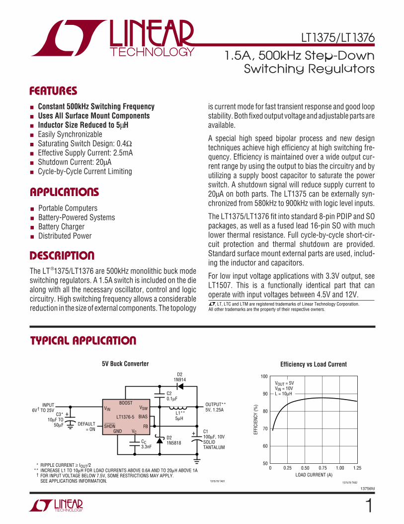
1 LT1375/LT1376 13756fd APPLICATIO S U DESCRIPTIO U FEATURES TYPICAL APPLICATIO U 1.5A, 500kHz Step-Down Switching Regulators ■ Constant 500kHz Switching Frequency ■ Uses All Surface Mount Components ■ Inductor Size Reduced to 5μ H ■ Easily Synchronizable ■ Saturating Switch Design: 0.4Ω ■ Effective Supply Current: 2.5mA ■ Shutdown Current: 20μ A ■ Cycle-by-Cycle Current Limiting ■ Portable Computers ■ Battery-Powered Systems ■ Battery Charger ■ Distributed Power The LT ® 1375/LT1376 are 500kHz monolithic buck mode switching regulators. A 1.5A switch is included on the die along with all the necessary oscillator, control and logic circuitry. High switching frequency allows a considerable reduction in the size of external components. The topology is current mode for fast transient response and good loop stability. Both fixed output voltage and adjustable parts are available. A special high speed bipolar process and new design techniques achieve high efficiency at high switching fre- quency. Efficiency is maintained over a wide output cur- rent range by using the output to bias the circuitry and by utilizing a supply boost capacitor to saturate the power switch. A shutdown signal will reduce supply current to 20μ A on both parts. The LT1375 can be externally syn- chronized from 580kHz to 900kHz with logic level inputs. The LT1375/LT1376 fit into standard 8-pin PDIP and SO packages, as well as a fused lead 16-pin SO with much lower thermal resistance. Full cycle-by-cycle short-cir- cuit protection and thermal shutdown are provided. Standard surface mount external parts are used, includ- ing the inductor and capacitors. For low input voltage applications with 3.3V output, see LT1507. This is a functionally identical part that can operate with input voltages between 4.5V and 12V. 5V Buck Converter LOAD CURRENT (A) 0 EFFICIENCY (%) 100 90 80 70 60 50 1.00 1375/76 TA02 0.25 0.50 0.75 1.25 V OUT = 5V V IN = 10V L = 10μH Efficiency vs Load Current BOOST LT1376-5 V IN OUTPUT** 5V, 1.25A * RIPPLE CURRENT ≥ I OUT /2 ** INCREASE L1 TO 10μH FOR LOAD CURRENTS ABOVE 0.6A AND TO 20μH ABOVE 1A † FOR INPUT VOLTAGE BELOW 7.5V, SOME RESTRICTIONS MAY APPLY. SEE APPLICATIONS INFORMATION. INPUT 6V † TO 25V 1375/76 TA01 C2 0.1μF C C 3.3nF D2 1N5818 C1 100μF, 10V SOLID TANTALUM C3* 10μF TO 50μF D2 1N914 L1** 5μH V SW FB BIAS GND V C DEFAULT = ON SHDN + + , LT, LTC and LTM are registered trademarks of Linear Technology Corporation. All other trademarks are the property of their respective owners.
Transcript of LT1375/LT1376 1.5A, 500kHz Step-Down · 13755 1375HV 1375I 1375I5 375HVI 1376 13765 1376HV 1376I...
1
LT1375/LT1376
13756fd
APPLICATIO SU
DESCRIPTIOU
FEATURES
TYPICAL APPLICATIO
U
1.5A, 500kHz Step-DownSwitching Regulators
Constant 500kHz Switching Frequency Uses All Surface Mount Components Inductor Size Reduced to 5µH Easily Synchronizable Saturating Switch Design: 0.4Ω Effective Supply Current: 2.5mA Shutdown Current: 20µA Cycle-by-Cycle Current Limiting
Portable Computers Battery-Powered Systems Battery Charger Distributed Power
The LT®1375/LT1376 are 500kHz monolithic buck modeswitching regulators. A 1.5A switch is included on the diealong with all the necessary oscillator, control and logiccircuitry. High switching frequency allows a considerablereduction in the size of external components. The topology
is current mode for fast transient response and good loopstability. Both fixed output voltage and adjustable parts areavailable.
A special high speed bipolar process and new designtechniques achieve high efficiency at high switching fre-quency. Efficiency is maintained over a wide output cur-rent range by using the output to bias the circuitry and byutilizing a supply boost capacitor to saturate the powerswitch. A shutdown signal will reduce supply current to20µA on both parts. The LT1375 can be externally syn-chronized from 580kHz to 900kHz with logic level inputs.
The LT1375/LT1376 fit into standard 8-pin PDIP and SOpackages, as well as a fused lead 16-pin SO with muchlower thermal resistance. Full cycle-by-cycle short-cir-cuit protection and thermal shutdown are provided.Standard surface mount external parts are used, includ-ing the inductor and capacitors.
For low input voltage applications with 3.3V output, seeLT1507. This is a functionally identical part that canoperate with input voltages between 4.5V and 12V.
5V Buck Converter
LOAD CURRENT (A)0
EFFI
CIEN
CY (%
)
100
90
80
70
60
501.00
1375/76 TA02
0.25 0.50 0.75 1.25
VOUT = 5VVIN = 10VL = 10µH
Efficiency vs Load Current
BOOST
LT1376-5
VINOUTPUT**5V, 1.25A
* RIPPLE CURRENT ≥ IOUT/2** INCREASE L1 TO 10µH FOR LOAD CURRENTS ABOVE 0.6A AND TO 20µH ABOVE 1A
† FOR INPUT VOLTAGE BELOW 7.5V, SOME RESTRICTIONS MAY APPLY.SEE APPLICATIONS INFORMATION.
INPUT6V† TO 25V
1375/76 TA01
C20.1µF
CC3.3nF
D21N5818
C1100µF, 10VSOLIDTANTALUM
C3*10µF TO
50µF
D21N914
L1**5µH
VSW
FB
BIAS
GND VC
DEFAULT= ON
SHDN
+
+
, LT, LTC and LTM are registered trademarks of Linear Technology Corporation.All other trademarks are the property of their respective owners.
2
LT1375/LT1376
13756fd
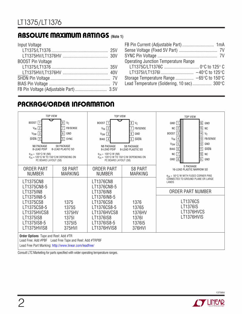
ABSOLUTE MAXIMUM RATINGS
W WW U
Input VoltageLT1375/LT1376 .................................................. 25VLT1375HV/LT1376HV ........................................ 30V
BOOST Pin VoltageLT1375/LT1376 .................................................. 35VLT1375HV/LT1376HV ........................................ 40V
SHDN Pin Voltage ..................................................... 7VBIAS Pin Voltage ...................................................... 7VFB Pin Voltage (Adjustable Part) ............................ 3.5V
FB Pin Current (Adjustable Part) ............................ 1mASense Voltage (Fixed 5V Part) .................................. 7VSYNC Pin Voltage ..................................................... 7VOperating Junction Temperature Range
LT1375C/LT1376C ............................... 0°C to 125° CLT1375I/LT1376I ............................. – 40°C to 125°C
Storage Temperature Range ................ – 65°C to 150°CLead Temperature (Soldering, 10 sec)................. 300°C
(Note 1)
PACKAGE/ORDER INFORMATION
W UU
TOP VIEW
S PACKAGE16-LEAD PLASTIC NARROW SO
1
2
3
4
5
6
7
8
16
15
14
13
12
11
10
9
GND
NC
BOOST
VIN
VSW
BIAS
NC
GND
GND
NC
VC
FB/SENSE
GND
SHDN
NC
GND
ORDER PART NUMBER
θJA = 50°C/ W WITH FUSED CORNER PINSCONNECTED TO GROUND PLANE OR LARGELANDS
1
2
3
4
8
7
6
5
TOP VIEW
BOOST
VIN
VSW
BIAS
N8 PACKAGE8-LEAD PDIP
S8 PACKAGE8-LEAD PLASTIC SO
VC
FB/SENSE
GND
SHDN
θJA = 100°C/ W (N8)θJA = 120°C/ W TO 150°C/W DEPENDING ON
PC BOARD LAYOUT (S8)
1
2
3
4
8
7
6
5
TOP VIEW
VC
FB/SENSE
GND
SYNC
N8 PACKAGE8-LEAD PDIP
S8 PACKAGE8-LEAD PLASTIC SO
BOOST
VIN
VSW
SHDN
θJA = 100°C/ W (N8)θJA = 120°C/ W TO 150°C/W DEPENDING ON
PC BOARD LAYOUT (S8)
LT1375CN8LT1375CN8-5LT1375IN8LT1375IN8-5LT1375CS8LT1375CS8-5LT1375HVCS8LT1375IS8LT1375IS8-5LT1375HVIS8
ORDER PARTNUMBER
LT1376CN8LT1376CN8-5LT1376IN8LT1376IN8-5LT1376CS8LT1376CS8-5LT1376HVCS8LT1376IS8LT1376IS8-5LT1376HVIS8
S8 PARTMARKING
1375137551375HV1375I1375I5375HVI
1376137651376HV1376I1376I5376HVI
LT1376CSLT1376ISLT1376HVCSLT1376HVIS
ORDER PARTNUMBER
S8 PARTMARKING
Order Options Tape and Reel: Add #TRLead Free: Add #PBF Lead Free Tape and Reel: Add #TRPBFLead Free Part Marking: http://www.linear.com/leadfree/
Consult LTC Marketing for parts specified with wider operating temperature ranges.
3
LT1375/LT1376
13756fd
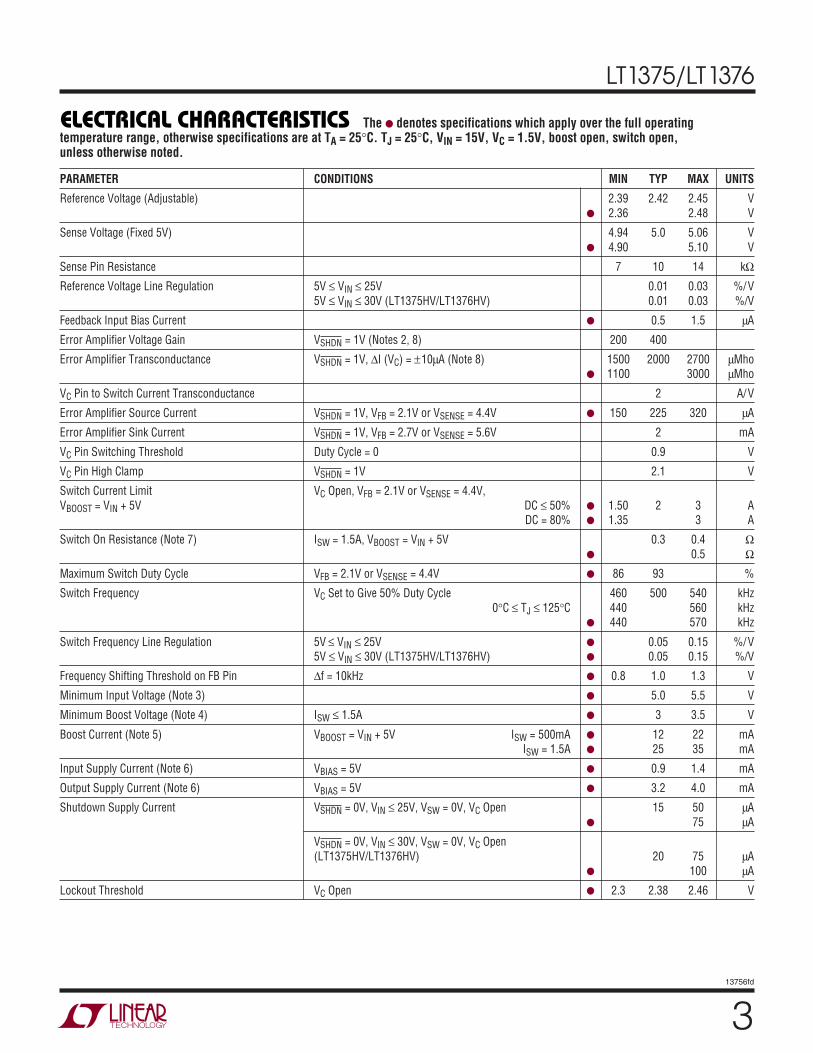
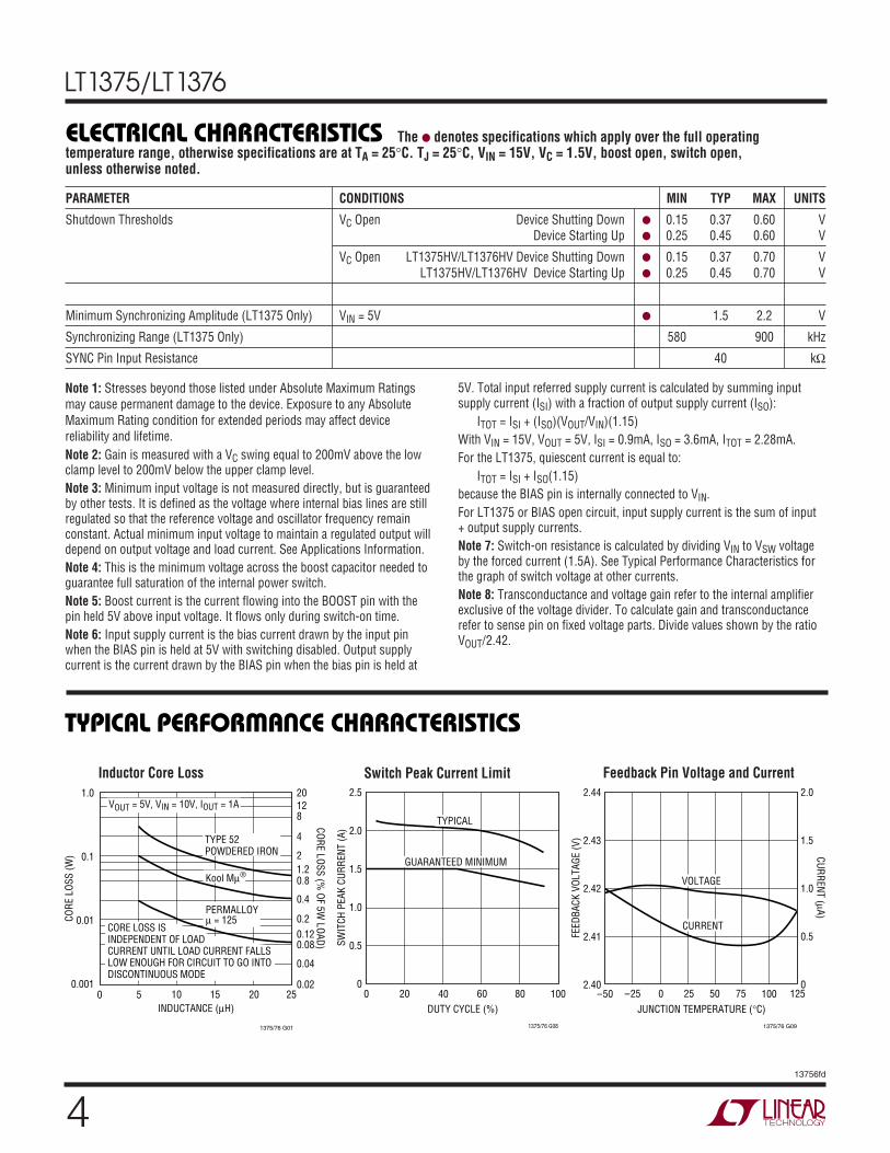
ELECTRICAL CHARACTERISTICS The denotes specifications which apply over the full operatingtemperature range, otherwise specifications are at TA = 25°C. TJ = 25°C, VIN = 15V, VC = 1.5V, boost open, switch open,unless otherwise noted.
PARAMETER CONDITIONS MIN TYP MAX UNITS
Reference Voltage (Adjustable) 2.39 2.42 2.45 V 2.36 2.48 V
Sense Voltage (Fixed 5V) 4.94 5.0 5.06 V 4.90 5.10 V
Sense Pin Resistance 7 10 14 kΩReference Voltage Line Regulation 5V ≤ VIN ≤ 25V 0.01 0.03 %/V
5V ≤ VIN ≤ 30V (LT1375HV/LT1376HV) 0.01 0.03 %/V
Feedback Input Bias Current 0.5 1.5 µA
Error Amplifier Voltage Gain VSHDN = 1V (Notes 2, 8) 200 400
Error Amplifier Transconductance VSHDN = 1V, ∆I (VC) = ±10µA (Note 8) 1500 2000 2700 µMho 1100 3000 µMho
VC Pin to Switch Current Transconductance 2 A/V
Error Amplifier Source Current VSHDN = 1V, VFB = 2.1V or VSENSE = 4.4V 150 225 320 µA
Error Amplifier Sink Current VSHDN = 1V, VFB = 2.7V or VSENSE = 5.6V 2 mA
VC Pin Switching Threshold Duty Cycle = 0 0.9 V
VC Pin High Clamp VSHDN = 1V 2.1 V
Switch Current Limit VC Open, VFB = 2.1V or VSENSE = 4.4V,VBOOST = VIN + 5V DC ≤ 50% 1.50 2 3 A
DC = 80% 1.35 3 A
Switch On Resistance (Note 7) ISW = 1.5A, VBOOST = VIN + 5V 0.3 0.4 Ω 0.5 Ω
Maximum Switch Duty Cycle VFB = 2.1V or VSENSE = 4.4V 86 93 %
Switch Frequency VC Set to Give 50% Duty Cycle 460 500 540 kHz0°C ≤ TJ ≤ 125°C 440 560 kHz
440 570 kHz
Switch Frequency Line Regulation 5V ≤ VIN ≤ 25V 0.05 0.15 %/V5V ≤ VIN ≤ 30V (LT1375HV/LT1376HV) 0.05 0.15 %/V
Frequency Shifting Threshold on FB Pin ∆f = 10kHz 0.8 1.0 1.3 V
Minimum Input Voltage (Note 3) 5.0 5.5 V
Minimum Boost Voltage (Note 4) ISW ≤ 1.5A 3 3.5 V
Boost Current (Note 5) VBOOST = VIN + 5V ISW = 500mA 12 22 mAISW = 1.5A 25 35 mA
Input Supply Current (Note 6) VBIAS = 5V 0.9 1.4 mA
Output Supply Current (Note 6) VBIAS = 5V 3.2 4.0 mA
Shutdown Supply Current VSHDN = 0V, VIN ≤ 25V, VSW = 0V, VC Open 15 50 µA 75 µA
VSHDN = 0V, VIN ≤ 30V, VSW = 0V, VC Open(LT1375HV/LT1376HV) 20 75 µA
100 µA
Lockout Threshold VC Open 2.3 2.38 2.46 V
4
LT1375/LT1376
13756fd
ELECTRICAL CHARACTERISTICS
Note 1: Stresses beyond those listed under Absolute Maximum Ratingsmay cause permanent damage to the device. Exposure to any AbsoluteMaximum Rating condition for extended periods may affect devicereliability and lifetime.Note 2: Gain is measured with a VC swing equal to 200mV above the lowclamp level to 200mV below the upper clamp level.Note 3: Minimum input voltage is not measured directly, but is guaranteedby other tests. It is defined as the voltage where internal bias lines are stillregulated so that the reference voltage and oscillator frequency remainconstant. Actual minimum input voltage to maintain a regulated output willdepend on output voltage and load current. See Applications Information.Note 4: This is the minimum voltage across the boost capacitor needed toguarantee full saturation of the internal power switch.Note 5: Boost current is the current flowing into the BOOST pin with thepin held 5V above input voltage. It flows only during switch-on time.Note 6: Input supply current is the bias current drawn by the input pinwhen the BIAS pin is held at 5V with switching disabled. Output supplycurrent is the current drawn by the BIAS pin when the bias pin is held at
5V. Total input referred supply current is calculated by summing inputsupply current (ISI) with a fraction of output supply current (ISO):
ITOT = ISI + (ISO)(VOUT/VIN)(1.15)With VIN = 15V, VOUT = 5V, ISI = 0.9mA, ISO = 3.6mA, ITOT = 2.28mA.For the LT1375, quiescent current is equal to:
ITOT = ISI + ISO(1.15)because the BIAS pin is internally connected to VIN.For LT1375 or BIAS open circuit, input supply current is the sum of input+ output supply currents.Note 7: Switch-on resistance is calculated by dividing VIN to VSW voltageby the forced current (1.5A). See Typical Performance Characteristics forthe graph of switch voltage at other currents.Note 8: Transconductance and voltage gain refer to the internal amplifierexclusive of the voltage divider. To calculate gain and transconductancerefer to sense pin on fixed voltage parts. Divide values shown by the ratioVOUT/2.42.
The denotes specifications which apply over the full operatingtemperature range, otherwise specifications are at TA = 25°C. TJ = 25°C, VIN = 15V, VC = 1.5V, boost open, switch open,unless otherwise noted.
PARAMETER CONDITIONS MIN TYP MAX UNITS
Shutdown Thresholds VC Open Device Shutting Down 0.15 0.37 0.60 VDevice Starting Up 0.25 0.45 0.60 V
VC Open LT1375HV/LT1376HV Device Shutting Down 0.15 0.37 0.70 VLT1375HV/LT1376HV Device Starting Up 0.25 0.45 0.70 V
Minimum Synchronizing Amplitude (LT1375 Only) VIN = 5V 1.5 2.2 V
Synchronizing Range (LT1375 Only) 580 900 kHz
SYNC Pin Input Resistance 40 kΩ
INDUCTANCE (µH)0 5
CORE
LOS
S (W
)
CORE LOSS (% OF 5W
LOAD)
1.0
0.1
0.01
0.00110 15 20
20128
4
21.20.8
0.4
0.20.120.08
0.04
0.0225
1375/76 G01
TYPE 52POWDERED IRON
Kool Mµ®
PERMALLOYµ = 125
VOUT = 5V, VIN = 10V, IOUT = 1A
CORE LOSS ISINDEPENDENT OF LOADCURRENT UNTIL LOAD CURRENT FALLSLOW ENOUGH FOR CIRCUIT TO GO INTODISCONTINUOUS MODE
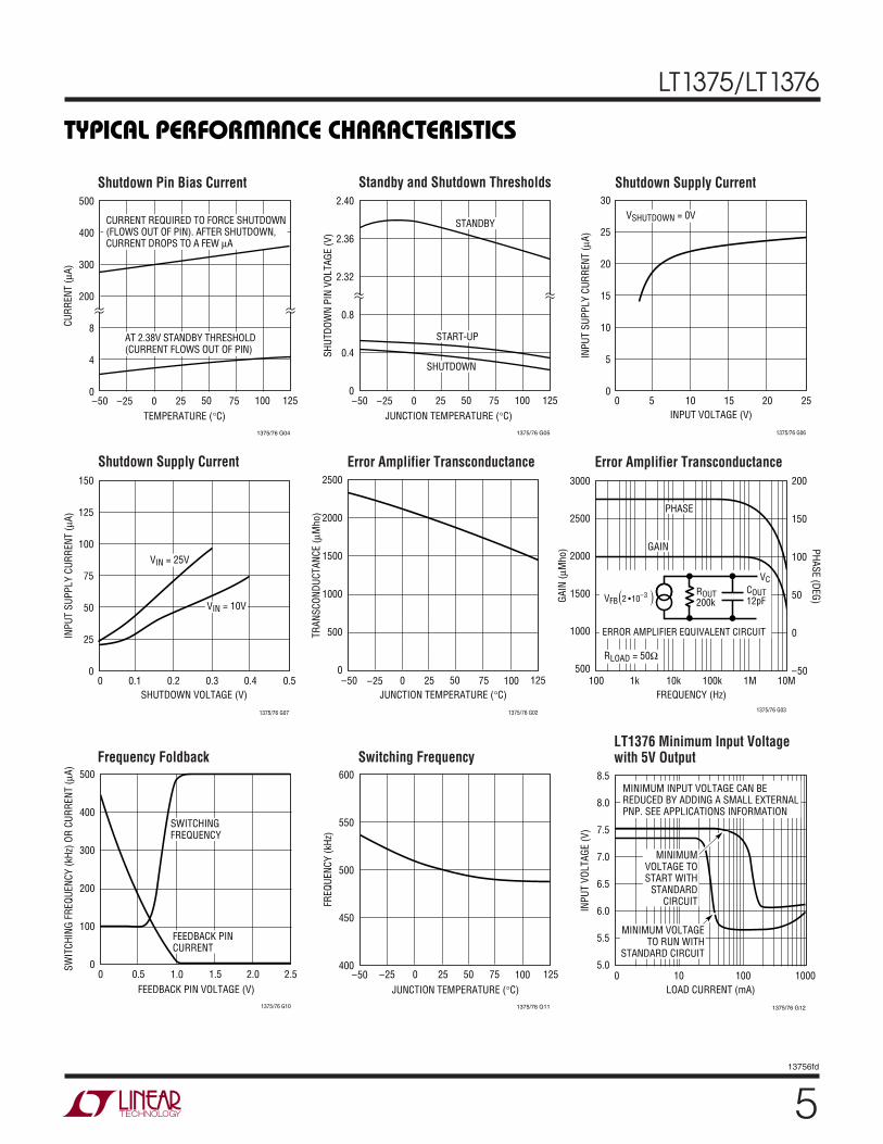
Inductor Core Loss
TYPICAL PERFORMANCE CHARACTERISTICS
UW
DUTY CYCLE (%)0
SWIT
CH P
EAK
CURR
ENT
(A)
2.5
2.0
1.5
1.0
0.5
080
1375/76 G08
20 40 60 100
TYPICAL
GUARANTEED MINIMUM
Switch Peak Current Limit
JUNCTION TEMPERATURE (°C)–50
2.44
2.43
2.42
2.41
2.40100
1375/76 G09
–25 0 25 50 75 125
FEED
BACK
VOL
TAGE
(V)
CURRENT (µA)
2.0
1.5
1.0
0.5
0
VOLTAGE
CURRENT
Feedback Pin Voltage and Current
5
LT1375/LT1376
13756fd
TYPICAL PERFORMANCE CHARACTERISTICS
UW
TEMPERATURE (°C)–50
500
400
300
200
8
4
025 75
1375/76 G04
–25 0 50 100 125
CURR
ENT
(µA)
CURRENT REQUIRED TO FORCE SHUTDOWN(FLOWS OUT OF PIN). AFTER SHUTDOWN,CURRENT DROPS TO A FEW µA
AT 2.38V STANDBY THRESHOLD(CURRENT FLOWS OUT OF PIN)
Shutdown Pin Bias Current
JUNCTION TEMPERATURE (°C)–50
TRAN
SCON
DUCT
ANCE
(µM
ho)
2500
2000
1500
1000
500
00 50 75
1375/76 G02
–25 25 100 125
Error Amplifier Transconductance
FREQUENCY (Hz)
GAIN
(µM
ho) PHASE (DEG)
3000
2500
2000
1500
1000
500
200
150
100
50
0
–50100 10k 100k 10M
1375/76 G03
1k 1M
GAIN
PHASE
ERROR AMPLIFIER EQUIVALENT CIRCUIT
ROUT200k
COUT12pF
VC
RLOAD = 50Ω
VFB 2 • 10–3 )(
Error Amplifier Transconductance
Frequency Foldback
LOAD CURRENT (mA)0
INPU
T VO
LTAG
E (V
)
8.5
8.0
7.5
7.0
6.5
6.0
5.5
5.010 100 1000
1375/76 G12
MINIMUM INPUT VOLTAGE CAN BEREDUCED BY ADDING A SMALL EXTERNALPNP. SEE APPLICATIONS INFORMATION
MINIMUMVOLTAGE TOSTART WITH
STANDARDCIRCUIT
MINIMUM VOLTAGETO RUN WITH
STANDARD CIRCUIT
LT1376 Minimum Input Voltagewith 5V Output
Shutdown Supply Current
INPUT VOLTAGE (V)0
INPU
T SU
PPLY
CUR
RENT
(µA)
30
25
20
15
10
5
05 10 15 20
1375/76 G06
25
VSHUTDOWN = 0V
JUNCTION TEMPERATURE (°C)–50
2.40
2.36
2.32
0.8
0.4
025 75
1375/76 G05
–25 0 50 100 125
SHUT
DOW
N PI
N VO
LTAG
E (V
)
STANDBY
START-UP
SHUTDOWN
Standby and Shutdown Thresholds
Shutdown Supply Current
SHUTDOWN VOLTAGE (V)0
INPU
T SU
PPLY
CUR
RENT
(µA)
150
125
100
75
50
25
00.1 0.2 0.3 0.4
1375/76 G07
0.5
VIN = 25V
VIN = 10V
FEEDBACK PIN VOLTAGE (V)0
SWIT
CHIN
G FR
EQUE
NCY
(kHz
) OR
CURR
ENT
(µA) 500
400
300
200
100
02.0
1375/76 G10
0.5 1.0 1.5 2.5
SWITCHINGFREQUENCY
FEEDBACK PINCURRENT
Switching Frequency
JUNCTION TEMPERATURE (°C)–50
600
550
500
450
400100
1375/76 G11
–25 0 25 50 75 125
FREQ
UENC
Y (k
Hz)
6
LT1375/LT1376
13756fd
TYPICAL PERFORMANCE CHARACTERISTICS
UW
INPUT VOLTAGE (V)0
CURR
ENT
(A)
1.50
1.25
1.00
0.75
0.50
0.25
05 10 15 20
1375/76 G13
25
L = 20µH
L = 10µH
L = 5µH
VOUT = 10V
INPUT VOLTAGE (V)0
CURR
ENT
(A)
1.50
1.25
1.00
0.75
0.50
0.25
05 10 15 20
1375/76 G14
25
L = 20µH
L = 10µH
L = 5µH
VOUT = 3.3V
Maximum Load Currentat VOUT = 10V
Maximum Load Currentat VOUT = 3.3V
Maximum Load Currentat VOUT = 5V
INPUT VOLTAGE (V)0
CURR
ENT
(A)
1.50
1.25
1.00
0.75
0.50
0.25
05 10 15 20
1375/76 G15
25
L = 20µH
L = 10µH
L = 5µH
VOUT = 5V
PIN FUNCTIONS
UUU
BOOST: The BOOST pin is used to provide a drive voltage,higher than the input voltage, to the internal bipolar NPNpower switch. Without this added voltage, the typicalswitch voltage loss would be about 1.5V. The additionalboost voltage allows the switch to saturate and voltageloss approximates that of a 0.3Ω FET structure, but withmuch smaller die area. Efficiency improves from 75% forconventional bipolar designs to > 87% for these new parts.
VSW: The switch pin is the emitter of the on-chip powerNPN switch. It is driven up to the input pin voltage duringswitch on time. Inductor current drives the switch pinnegative during switch off time. Negative voltage is clamped
with the external catch diode. Maximum negative switchvoltage allowed is –0.8V.
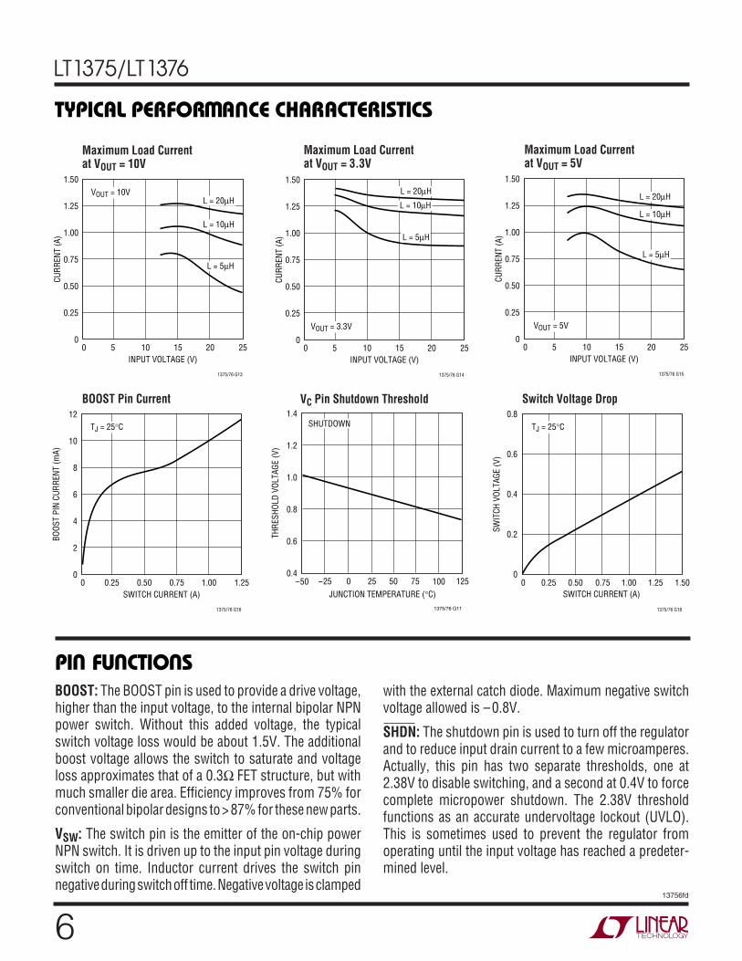
SHDN: The shutdown pin is used to turn off the regulatorand to reduce input drain current to a few microamperes.Actually, this pin has two separate thresholds, one at2.38V to disable switching, and a second at 0.4V to forcecomplete micropower shutdown. The 2.38V thresholdfunctions as an accurate undervoltage lockout (UVLO).This is sometimes used to prevent the regulator fromoperating until the input voltage has reached a predeter-mined level.
SWITCH CURRENT (A)0
BOOS
T PI
N CU
RREN
T (m
A)
12
10
8
6
4
2
00.25 0.50 0.75 1.00
1375/76 G16
1.25
TJ = 25°C
BOOST Pin Current VC Pin Shutdown Threshold
SWITCH CURRENT (A)0
SWIT
CH V
OLTA
GE (V
)
0.8
0.6
0.4
0.2
00.25 0.50 0.75 1.00
1375/76 G18
1.25 1.50
TJ = 25°C
Switch Voltage Drop
JUNCTION TEMPERATURE (°C)–50
1.4
1.2
1.0
0.8
0.6
0.4100
1375/76 G11
–25 0 25 50 75 125
THRE
SHOL
D VO
LTAG
E (V
)
SHUTDOWN
7
LT1375/LT1376
13756fd
PIN FUNCTIONS
UUU
VIN: This is the collector of the on-chip power NPN switch.This pin powers the internal circuitry and internal regulatorwhen the BIAS pin is not present. At NPN switch on and off,high dl/dt edges occur on this pin. Keep the externalbypass and catch diode close to this pin. All trace induc-tance on this path will create a voltage spike at switch off,adding to the VCE voltage across the internal NPN.
BIAS (LT1376 Only): The BIAS pin is used to improveefficiency when operating at higher input voltages andlight load current. Connecting this pin to the regulatedoutput voltage forces most of the internal circuitry to drawits operating current from the output voltage rather thanthe input supply. This is a much more efficient way ofdoing business if the input voltage is much higher than theoutput. Minimum output voltage setting for this mode ofoperation is 3.3V. Efficiency improvement at VIN = 20V,VOUT = 5V, and IOUT = 25mA is over 10%.
SYNC (LT1375 Only): The SYNC pin is used to synchro-nize the internal oscillator to an external signal. It is directlylogic compatible and can be driven with any signal be-tween 10% and 90% duty cycle. The synchronizing rangeis equal to initial operating frequency, up to 900kHz. SeeSynchronizing section in Applications Information fordetails.
FB/SENSE: The feedback pin is used to set output voltage,using an external voltage divider that generates 2.42V atthe pin with the desired output voltage. The fixed voltage(-5) parts have the divider included on the chip, and the FB
pin is used as a SENSE pin, connected directly to the 5Voutput. Two additional functions are performed by the FBpin. When the pin voltage drops below 1.7V, switchcurrent limit is reduced. Below 1V, switching frequency isalso reduced. See Feedback Pin Function section in Appli-cations Information for details.
VC: The VC pin is the output of the error amplifier and theinput of the peak switch current comparator. It is normallyused for frequency compensation, but can do double dutyas a current clamp or control loop override. This pin sitsat about 1V for very light loads and 2V at maximum load.It can be driven to ground to shut off the regulator, but ifdriven high, current must be limited to 4mA.
GND: The GND pin connection needs consideration fortwo reasons. First, it acts as the reference for the regulatedoutput, so load regulation will suffer if the “ground” end ofthe load is not at the same voltage as the GND pin of theIC. This condition will occur when load current or othercurrents flow through metal paths between the GND pinand the load ground point. Keep the ground path shortbetween the GND pin and the load, and use a ground planewhen possible. The second consideration is EMI causedby GND pin current spikes. Internal capacitance betweenthe VSW pin and the GND pin creates very narrow (<10ns)current spikes in the GND pin. If the GND pin is connectedto system ground with a long metal trace, this trace mayradiate excess EMI. Keep the path between the inputbypass and the GND pin short.
BLOCK DIAGRAM
W
The LT1376 is a constant frequency, current mode buckconverter. This means that there is an internal clock andtwo feedback loops that control the duty cycle of the powerswitch. In addition to the normal error amplifier, there is acurrent sense amplifier that monitors switch current on acycle-by-cycle basis. A switch cycle starts with an oscilla-tor pulse which sets the RS flip-flop to turn the switch on.When switch current reaches a level set by the invertinginput of the comparator, the flip-flop is reset and theswitch turns off. Output voltage control is obtained byusing the output of the error amplifier to set the switchcurrent trip point. This technique means that the error
amplifier commands current to be delivered to the outputrather than voltage. A voltage fed system will have lowphase shift up to the resonant frequency of the inductorand output capacitor, then an abrupt 180° shift will occur.The current fed system will have 90° phase shift at a muchlower frequency, but will not have the additional 90° shiftuntil well beyond the LC resonant frequency. This makesit much easier to frequency compensate the feedback loopand also gives much quicker transient response.
Most of the circuitry of the LT1376 operates from aninternal 2.9V bias line. The bias regulator normally drawspower from the regulator input pin, but if the BIAS pin is
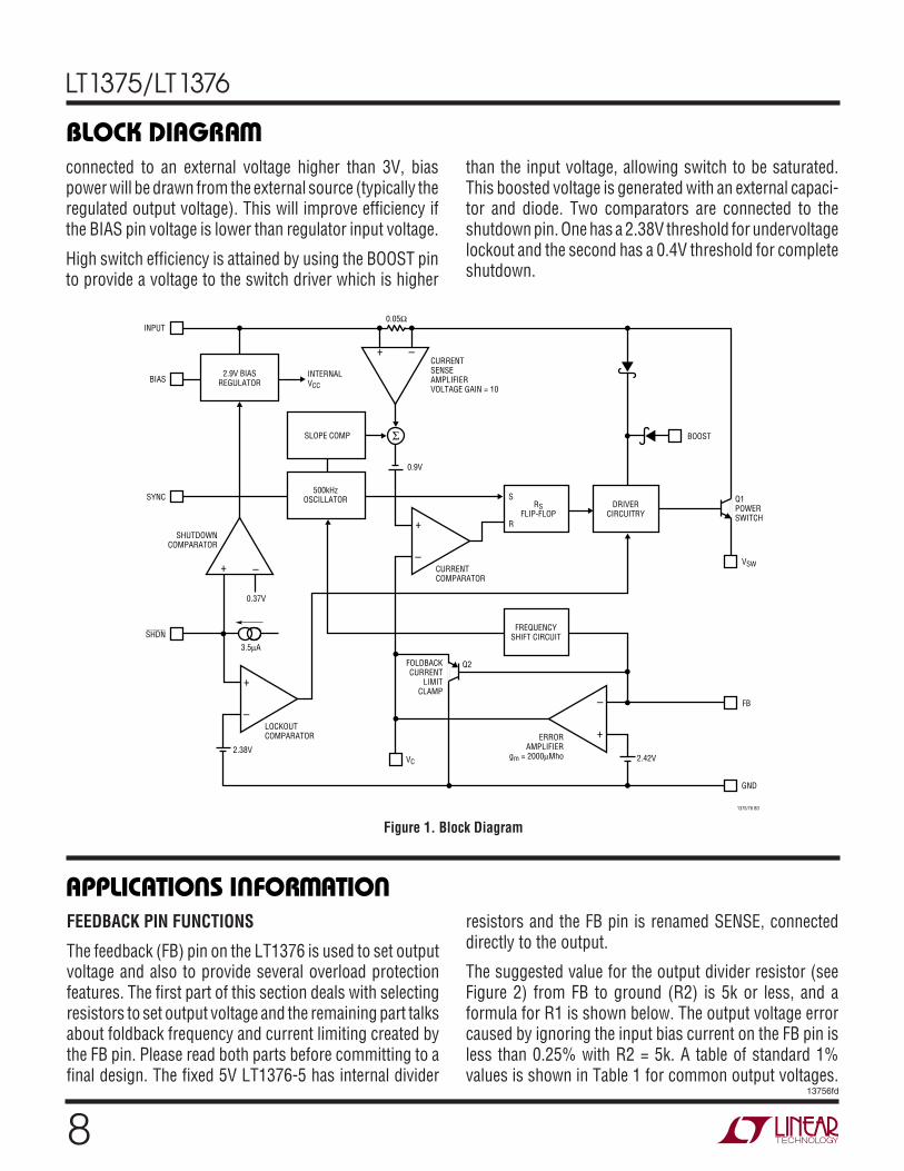
8
LT1375/LT1376
13756fd
connected to an external voltage higher than 3V, biaspower will be drawn from the external source (typically theregulated output voltage). This will improve efficiency ifthe BIAS pin voltage is lower than regulator input voltage.
High switch efficiency is attained by using the BOOST pinto provide a voltage to the switch driver which is higher
BLOCK DIAGRAM
W
than the input voltage, allowing switch to be saturated.This boosted voltage is generated with an external capaci-tor and diode. Two comparators are connected to theshutdown pin. One has a 2.38V threshold for undervoltagelockout and the second has a 0.4V threshold for completeshutdown.
–+
–
+
–
+
–
+
Σ
INPUT
2.9V BIASREGULATOR
500kHzOSCILLATOR
FREQUENCYSHIFT CIRCUIT
VSW
FB
VC
GND
1375/76 BD
SLOPE COMP
0.05Ω
BIASINTERNALVCC
CURRENTSENSEAMPLIFIERVOLTAGE GAIN = 10
SYNC
SHUTDOWNCOMPARATOR
CURRENTCOMPARATOR
ERRORAMPLIFIER
gm = 2000µMho
FOLDBACKCURRENT
LIMITCLAMP
BOOST
RSFLIP-FLOP
DRIVERCIRCUITRY
S
R
0.9V
LOCKOUTCOMPARATOR
0.37V
3.5µA
Q2
Q1POWERSWITCH
2.38V2.42V
–+
SHDN
Figure 1. Block Diagram
APPLICATIONS INFORMATION
WU UU
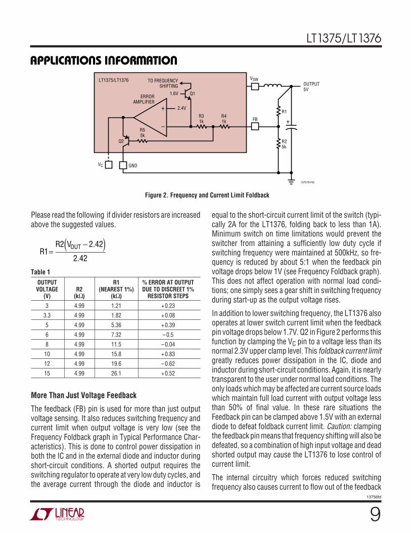
FEEDBACK PIN FUNCTIONS
The feedback (FB) pin on the LT1376 is used to set outputvoltage and also to provide several overload protectionfeatures. The first part of this section deals with selectingresistors to set output voltage and the remaining part talksabout foldback frequency and current limiting created bythe FB pin. Please read both parts before committing to afinal design. The fixed 5V LT1376-5 has internal divider
resistors and the FB pin is renamed SENSE, connecteddirectly to the output.
The suggested value for the output divider resistor (seeFigure 2) from FB to ground (R2) is 5k or less, and aformula for R1 is shown below. The output voltage errorcaused by ignoring the input bias current on the FB pin isless than 0.25% with R2 = 5k. A table of standard 1%values is shown in Table 1 for common output voltages.
9
LT1375/LT1376
13756fd
APPLICATIONS INFORMATION
WU UU
–
+ 2.4V
VSW
VC GND
1375/76 F02
TO FREQUENCYSHIFTING
R31k
R41k
R1
R25k
OUTPUT5V
R55k
ERRORAMPLIFIER
FB
1.6V Q1
LT1375/LT1376
Q2
+
Figure 2. Frequency and Current Limit Foldback
Please read the following if divider resistors are increasedabove the suggested values.
RR VOUT
12 2 42
2 42=
−( ).
.
Table 1OUTPUT R1 % ERROR AT OUTPUTVOLTAGE R2 (NEAREST 1%) DUE TO DISCREET 1%
(V) (kΩ) (kΩ) RESISTOR STEPS
3 4.99 1.21 +0.23
3.3 4.99 1.82 +0.08
5 4.99 5.36 +0.39
6 4.99 7.32 –0.5
8 4.99 11.5 –0.04
10 4.99 15.8 +0.83
12 4.99 19.6 –0.62
15 4.99 26.1 +0.52
More Than Just Voltage Feedback
The feedback (FB) pin is used for more than just outputvoltage sensing. It also reduces switching frequency andcurrent limit when output voltage is very low (see theFrequency Foldback graph in Typical Performance Char-acteristics). This is done to control power dissipation inboth the IC and in the external diode and inductor duringshort-circuit conditions. A shorted output requires theswitching regulator to operate at very low duty cycles, andthe average current through the diode and inductor is
equal to the short-circuit current limit of the switch (typi-cally 2A for the LT1376, folding back to less than 1A).Minimum switch on time limitations would prevent theswitcher from attaining a sufficiently low duty cycle ifswitching frequency were maintained at 500kHz, so fre-quency is reduced by about 5:1 when the feedback pinvoltage drops below 1V (see Frequency Foldback graph).This does not affect operation with normal load condi-tions; one simply sees a gear shift in switching frequencyduring start-up as the output voltage rises.
In addition to lower switching frequency, the LT1376 alsooperates at lower switch current limit when the feedbackpin voltage drops below 1.7V. Q2 in Figure 2 performs thisfunction by clamping the VC pin to a voltage less than itsnormal 2.3V upper clamp level. This foldback current limitgreatly reduces power dissipation in the IC, diode andinductor during short-circuit conditions. Again, it is nearlytransparent to the user under normal load conditions. Theonly loads which may be affected are current source loadswhich maintain full load current with output voltage lessthan 50% of final value. In these rare situations theFeedback pin can be clamped above 1.5V with an externaldiode to defeat foldback current limit. Caution: clampingthe feedback pin means that frequency shifting will also bedefeated, so a combination of high input voltage and deadshorted output may cause the LT1376 to lose control ofcurrent limit.
The internal circuitry which forces reduced switchingfrequency also causes current to flow out of the feedback
10
LT1375/LT1376
13756fd
APPLICATIONS INFORMATION
WU UU
pin when output voltage is low. The equivalent circuitry isshown in Figure 2. Q1 is completely off during normaloperation. If the FB pin falls below 1V, Q1 begins toconduct current and reduces frequency at the rate ofapproximately 5kHz/µA. To ensure adequate frequencyfoldback (under worst-case short-circuit conditions), theexternal divider Thevinin resistance must be low enoughto pull 150µA out of the FB pin with 0.6V on the pin (RDIV≤ 4k). The net result is that reductions in frequency andcurrent limit are affected by output voltage divider imped-ance. Although divider impedance is not critical, cautionshould be used if resistors are increased beyond thesuggested values and short-circuit conditions will occurwith high input voltage. High frequency pickup will in-crease and the protection accorded by frequency andcurrent foldback will decrease.
MAXIMUM OUTPUT LOAD CURRENT
Maximum load current for a buck converter is limited bythe maximum switch current rating (IP) of the LT1376.This current rating is 1.5A up to 50% duty cycle (DC),decreasing to 1.35A at 80% duty cycle. This is showngraphically in Typical Performance Characteristics and asshown in the formula below:
IP = 1.5A for DC ≤ 50%IP = 1.65A – 0.15 (DC) – 0.26 (DC)2 for 50% < DC < 90%
DC = Duty cycle = VOUT/VIN
Example: with VOUT = 5V, VIN = 8V; DC = 5/8 = 0.625, and;
ISW(MAX) = 1.64 – 0.15 (0.625) – 0.26 (0.625)2 = 1.44A
Current rating decreases with duty cycle because theLT1376 has internal slope compensation to prevent cur-rent mode subharmonic switching. For more details, readApplication Note 19. The LT1376 is a little unusual in thisregard because it has nonlinear slope compensation whichgives better compensation with less reduction in currentlimit.
Maximum load current would be equal to maximumswitch current for an infinitely large inductor, but withfinite inductor size, maximum load current is reduced byone-half peak-to-peak inductor current. The following
formula assumes continuous mode operation, implyingthat the term on the right is less than one-half of IP.
IOUT(MAX) =Continuous Mode
For the conditions above and L = 10µH,
I
A
OUT MAX( ) −= −
( ) −( )⎛⎝
⎞⎠⎛⎝
⎞⎠ ( )
= − =
1 445 8 5
2 10 500 10 8
1 44 0 19 1 25
5 3.
•
. . .
At VIN = 15V, duty cycle is 33%, so IP is just equal to a fixed1.5A, and IOUT(MAX) is equal to:
1 55 15 5
2 10 500 10 151 5 0 33 1 17
5 3.
•. . .−
( ) −( )⎛⎝
⎞⎠⎛⎝
⎞⎠ ( )
= − =−
A
Note that there is less load current available at the higherinput voltage because inductor ripple current increases.This is not always the case. Certain combinations ofinductor value and input voltage range may yield loweravailable load current at the lowest input voltage due toreduced peak switch current at high duty cycles. If loadcurrent is close to the maximum available, please checkmaximum available current at both input voltage ex-tremes. To calculate actual peak switch current with agiven set of conditions, use:
I IV V V
L f VSW PEAK OUT
OUT IN OUT
IN( ) = +
−( )( )( )( )2
For lighter loads where discontinuous operation can beused, maximum load current is equal to:
IOUT(MAX) =Discontinuous mode
I P −( ) −( )
( )( )( )V V V
L f V
OUT IN OUT
IN2
I f L V
V V V
P OUT
OUT IN OUT
( ) ( )( )( )( ) −( )
2
2
11
LT1375/LT1376
13756fd
APPLICATIONS INFORMATION
WU UU
must withstand continuous fault conditions. If maxi-mum load current is 0.5A, for instance, a 0.5A inductormay not survive a continuous 1.5A overload condition.Dead shorts will actually be more gentle on the induc-tor because the LT1376 has foldback current limiting.
2. Calculate peak inductor current at full load current toensure that the inductor will not saturate. Peak currentcan be significantly higher than output current, espe-cially with smaller inductors and lighter loads, so don’tomit this step. Powdered iron cores are forgivingbecause they saturate softly, whereas ferrite coressaturate abruptly. Other core materials fall in betweensomewhere. The following formula assumes continu-ous mode of operation, but it errs only slightly on thehigh side for discontinuous mode, so it can be used forall conditions.
I IV V V
f L VPEAK OUT
OUT IN OUT
IN
= +−( )
( )( )( )2
VIN = Maximum input voltagef = Switching frequency, 500kHz
3. Decide if the design can tolerate an “open” core geom-etry like a rod or barrel, which have high magnetic fieldradiation, or whether it needs a closed core like a toroidto prevent EMI problems. One would not want an opencore next to a magnetic storage media, for instance!This is a tough decision because the rods or barrels aretemptingly cheap and small and there are no helpfulguidelines to calculate when the magnetic field radia-tion will be a problem.
4. Start shopping for an inductor (see representativesurface mount units in Table 2) which meets the re-quirements of core shape, peak current (to avoid satu-ration), average current (to limit heating), and faultcurrent (if the inductor gets too hot, wire insulation willmelt and cause turn-to-turn shorts). Keep in mind thatall good things like high efficiency, low profile, and hightemperature operation will increase cost, sometimesdramatically. Get a quote on the cheapest unit first tocalibrate yourself on price, then ask for what you reallywant.
Example: with L = 2µH, VOUT = 5V, and VIN(MAX) = 15V,
I mAOUT MAX( )−
=( ) ⎛
⎝⎞⎠⎛⎝
⎞⎠( )
( ) −( ) =1 5 500 10 2 10 15
2 5 15 5338
2 3 6. • •
The main reason for using such a tiny inductor is that it isphysically very small, but keep in mind that peak-to-peakinductor current will be very high. This will increase outputripple voltage. If the output capacitor has to be made largerto reduce ripple voltage, the overall circuit could actuallywind up larger.
CHOOSING THE INDUCTOR AND OUTPUT CAPACITOR
For most applications the output inductor will fall in therange of 3µH to 20µH. Lower values are chosen to reducephysical size of the inductor. Higher values allow moreoutput current because they reduce peak current seen bythe LT1376 switch, which has a 1.5A limit. Higher valuesalso reduce output ripple voltage, and reduce core loss.Graphs in the Typical Performance Characteristics sectionshow maximum output load current versus inductor sizeand input voltage. A second graph shows core loss versusinductor size for various core materials.
When choosing an inductor you might have to considermaximum load current, core and copper losses, allowablecomponent height, output voltage ripple, EMI, fault cur-rent in the inductor, saturation, and of course, cost. Thefollowing procedure is suggested as a way of handlingthese somewhat complicated and conflicting requirements.
1. Choose a value in microhenries from the graphs ofmaximum load current and core loss. Choosing a smallinductor with lighter loads may result in discontinuousmode of operation, but the LT1376 is designed to workwell in either mode. Keep in mind that lower core lossmeans higher cost, at least for closed core geometrieslike toroids. The core loss graphs show both absoluteloss and percent loss for a 5W output, so actual percentlosses must be calculated for each situation.
Assume that the average inductor current is equal toload current and decide whether or not the inductor
12
LT1375/LT1376
13756fd
APPLICATIONS INFORMATION
WU UU
5. After making an initial choice, consider the secondarythings like output voltage ripple, second sourcing, etc.Use the experts in the Linear Technology’s applica-tions department if you feel uncertain about the finalchoice. They have experience with a wide range ofinductor types and can tell you about the latest devel-opments in low profile, surface mounting, etc.
Table 2SERIES CORE
VENDOR/ VALUE DC CORE RESIS- MATER- HEIGHTPART NO. (µH) (Amps) TYPE TANCE(Ω) IAL (mm)
Coiltronics
CTX5-1 5 2.3 Tor 0.027 KMµ 4.2
CTX10-1 10 1.9 Tor 0.039 KMµ 4.2
CTX20-1 20 1.0 Tor 0.137 KMµ 4.2
CTX15-2 15 1.8 Tor 0.058 KMµ 6.0
CTX20-3 20 1.5 Tor 0.093 KMµ 4.7
CTX20-4 20 2.2 Tor 0.059 KMµ 6.4
CTX5-1P 5 1.8 Tor 0.021 52 4.2
CTX10-1P 10 1.6 Tor 0.030 52 4.2
CTX15-1P 15 1.2 Tor 0.046 52 4.2
CTX20-1P 20 1.0 Tor 0.081 52 4.2
CTX20-2P 20 1.3 Tor 0.052 52 6.0
CTX20-4P 20 1.8 Tor 0.039 52 6.35
Sumida
CDRH64 10 1.7 SC 0.084 Fer 4.5
CDRH74 22 1.2 SC 0.077 Fer 4.5
CDRH73 10 1.7 SC 0.055 Fer 3.4
CDRH73 22 1.1 SC 0.15 Fer 3.4
CD73 10 1.4 Open 0.062 Fer 3.5
CD73 18 1.1 Open 0.085 Fer 3.5
CD104 10 2.4 Open 0.041 Fer 4.0
CD104 18 1.7 Open 0.062 Fer 4.0
Gowanda
SM20-102K 10 1.3 Open 0.038 Fer 7.0
SM20-152K 15 1.3 Open 0.049 Fer 7.0
SM20-222K 22 1.3 Open 0.059 Fer 7.0
Dale
IHSM-4825 10 3.1 Open 0.071 Fer 5.6
IHSM-4825 22 1.7 Open 0.152 Fer 5.6
IHSM-5832 10 4.3 Open 0.053 Fer 7.1
IHSM-5832 22 2.8 Open 0.12 Fer 7.1
IHSM-7832 22 3.8 Open 0.054 Fer 7.1
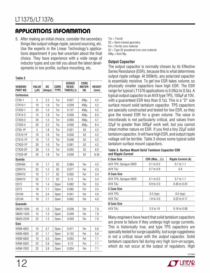
Tor = ToroidSC = Semi-closed geometryFer = Ferrite core material52 = Type 52 powdered iron core materialKMµ = Kool Mµ
Output CapacitorThe output capacitor is normally chosen by its EffectiveSeries Resistance (ESR), because this is what determinesoutput ripple voltage. At 500kHz, any polarized capacitoris essentially resistive. To get low ESR takes volume, sophysically smaller capacitors have high ESR. The ESRrange for typical LT1376 applications is 0.05Ω to 0.5Ω. Atypical output capacitor is an AVX type TPS, 100µF at 10V,with a guaranteed ESR less than 0.1Ω. This is a “D” sizesurface mount solid tantalum capacitor. TPS capacitorsare specially constructed and tested for low ESR, so theygive the lowest ESR for a given volume. The value inmicrofarads is not particularly critical, and values from22µF to greater than 500µF work well, but you cannotcheat mother nature on ESR. If you find a tiny 22µF solidtantalum capacitor, it will have high ESR, and output ripplevoltage will be terrible. Table 3 shows some typical solidtantalum surface mount capacitors.Table 3. Surface Mount Solid Tantalum Capacitor ESRand Ripple CurrentE Case Size ESR (Max., Ω) Ripple Current (A)
AVX TPS, Sprague 593D 0.1 to 0.3 0.7 to 1.1
AVX TAJ 0.7 to 0.9 0.4
D Case Size
AVX TPS, Sprague 593D 0.1 to 0.3 0.7 to 1.1
AVX TAJ 0.9 to 2.0 0.36 to 0.24
C Case Size
AVX TPS 0.2 (typ) 0.5 (typ)
AVX TAJ 1.8 to 3.0 0.22 to 0.17
B Case Size
AVX TAJ 2.5 to 10 0.16 to 0.08
Many engineers have heard that solid tantalum capacitorsare prone to failure if they undergo high surge currents.This is historically true, and type TPS capacitors arespecially tested for surge capability, but surge ruggednessis not a critical issue with the output capacitor. Solidtantalum capacitors fail during very high turn-on surges,which do not occur at the output of regulators. High
13
LT1375/LT1376
13756fd
APPLICATIONS INFORMATION
WU UU
discharge surges, such as when the regulator output isdead shorted, do not harm the capacitors.
Unlike the input capacitor, RMS ripple current in theoutput capacitor is normally low enough that ripple cur-rent rating is not an issue. The current waveform istriangular with a typical value of 200mARMS. The formulato calculate this is:
Output Capacitor Ripple Current (RMS):
IV V V
L f VRIPPLE RMS
OUT IN OUT
IN( ) =
( ) −( )( )( )( )
0 29.
Ceramic Capacitors
Higher value, lower cost ceramic capacitors are nowbecoming available in smaller case sizes. These are tempt-ing for switching regulator use because of their very lowESR. Unfortunately, the ESR is so low that it can causeloop stability problems. Solid tantalum capacitor’s ESRgenerates a loop “zero” at 5kHz to 50kHz that is instrumen-tal in giving acceptable loop phase margin. Ceramic ca-pacitors remain capacitive to beyond 300kHz and usuallyresonate with their ESL before ESR becomes effective.They are appropriate for input bypassing because of theirhigh ripple current ratings and tolerance of turn-on surges.For further information on ceramic and other capacitortypes please refer to Design Note 95.
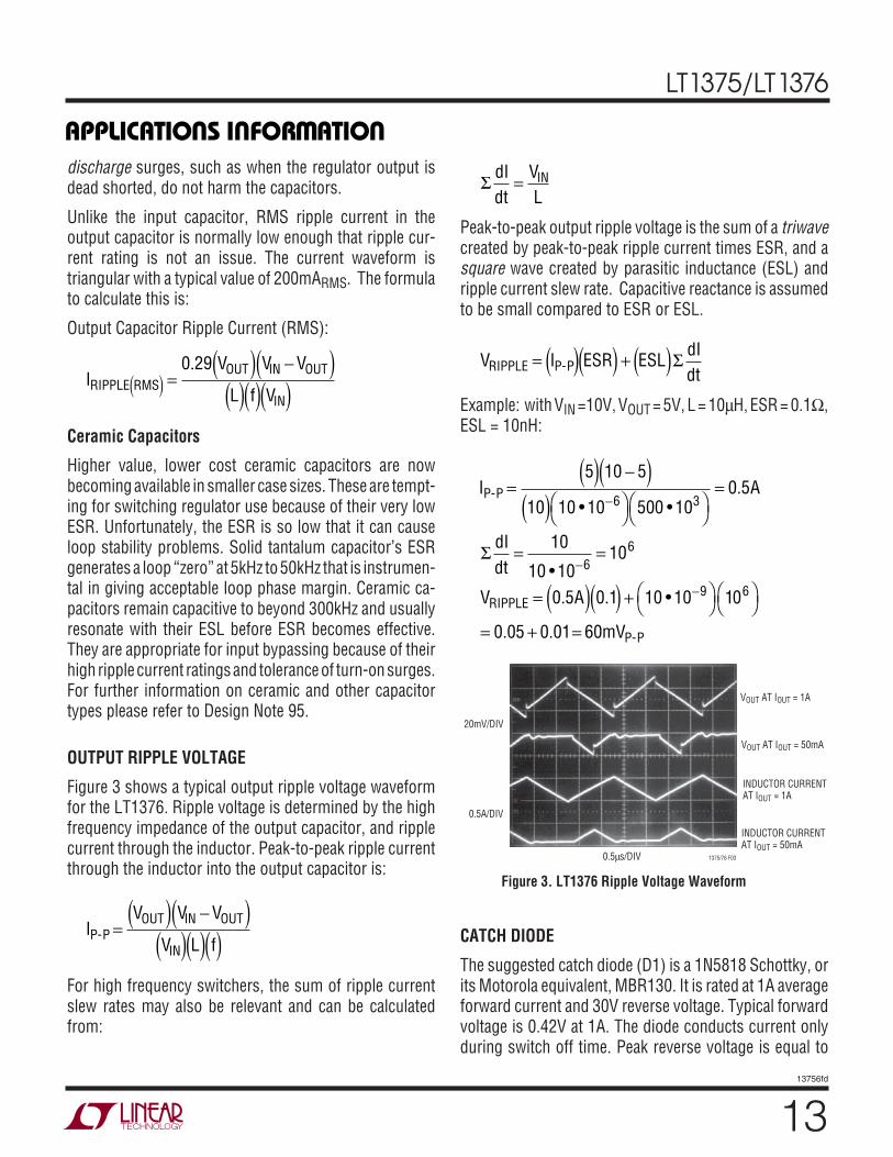
OUTPUT RIPPLE VOLTAGE
Figure 3 shows a typical output ripple voltage waveformfor the LT1376. Ripple voltage is determined by the highfrequency impedance of the output capacitor, and ripplecurrent through the inductor. Peak-to-peak ripple currentthrough the inductor into the output capacitor is:
IV V V
V L fP
OUT IN OUT
IN-P =
( ) −( )( )( )( )
For high frequency switchers, the sum of ripple currentslew rates may also be relevant and can be calculatedfrom:
Σ dIdt
VLIN=
Peak-to-peak output ripple voltage is the sum of a triwavecreated by peak-to-peak ripple current times ESR, and asquare wave created by parasitic inductance (ESL) andripple current slew rate. Capacitive reactance is assumedto be small compared to ESR or ESL.
V I ESR ESLdIdtRIPPLE = ( )( ) + ( )P-P Σ
Example: with VIN =10V, VOUT = 5V, L = 10µH, ESR = 0.1Ω,ESL = 10nH:
I A
dIdt
V A
mV
RIPPLE
P-P
P-P
=( ) −( )
( )⎛⎝ ⎞⎠⎛⎝
⎞⎠
=
= =
= ( )( ) + ⎛⎝
⎞⎠⎛⎝
⎞⎠
= + =
−
−
−
5 10 5
10 10 10 500 100 5
10
10 1010
0 5 0 1 10 10 10
0 05 0 01 60
6 3
66
9 6
• •.
•. . •
. .
Σ
VOUT AT IOUT = 1A
VOUT AT IOUT = 50mA
INDUCTOR CURRENTAT IOUT = 1A
0.5µs/DIV 1375/76 F03
Figure 3. LT1376 Ripple Voltage Waveform
INDUCTOR CURRENTAT IOUT = 50mA
20mV/DIV
0.5A/DIV
CATCH DIODE
The suggested catch diode (D1) is a 1N5818 Schottky, orits Motorola equivalent, MBR130. It is rated at 1A averageforward current and 30V reverse voltage. Typical forwardvoltage is 0.42V at 1A. The diode conducts current onlyduring switch off time. Peak reverse voltage is equal to
14
LT1375/LT1376
13756fd
APPLICATIONS INFORMATION
WU UU
regulator input voltage. Average forward current in normaloperation can be calculated from:
II V V
VD AVGOUT IN OUT
IN( ) =
−( )
This formula will not yield values higher than 1A withmaximum load current of 1.25A unless the ratio of inputto output voltage exceeds 5:1. The only reason to considera larger diode is the worst-case condition of a high inputvoltage and overloaded (not shorted) output. Under short-circuit conditions, foldback current limit will reduce diodecurrent to less than 1A, but if the output is overloaded anddoes not fall to less than 1/3 of nominal output voltage,foldback will not take effect. With the overloaded condi-tion, output current will increase to a typical value of 1.8A,determined by peak switch current limit of 2A. WithVIN = 15V, VOUT = 4V (5V overloaded) and IOUT = 1.8A:
I AD AVG( ) =−( )
=1 8 15 4
151 32
..
This is safe for short periods of time, but it would beprudent to check with the diode manufacturer if continu-ous operation under these conditions must be tolerated.
BOOST PIN CONSIDERATIONS
For most applications, the boost components are a 0.1µFcapacitor and a 1N914 or 1N4148 diode. The anode isconnected to the regulated output voltage and this gener-ates a voltage across the boost capacitor nearly identicalto the regulated output. In certain applications, the anodemay instead be connected to the unregulated input volt-age. This could be necessary if the regulated outputvoltage is very low (< 3V) or if the input voltage is less than6V. Efficiency is not affected by the capacitor value, but thecapacitor should have an ESR of less than 2Ω to ensurethat it can be recharged fully under the worst-case condi-tion of minimum input voltage. Almost any type of film orceramic capacitor will work fine.
WARNING! Peak voltage on the BOOST pin is the sum ofunregulated input voltage plus the voltage across theboost capacitor. This normally means that peak BOOST
pin voltage is equal to input voltage plus output voltage,but when the boost diode is connected to the regulatorinput, peak BOOST pin voltage is equal to twice the inputvoltage. Be sure that BOOST pin voltage does not exceedits maximum rating.
For nearly all applications, a 0.1uF boost capacitor worksjust fine, but for the curious, more details are providedhere. The size of the boost capacitor is determined byswitch drive current requirements. During switch on time,drain current on the capacitor is approximately 10mA +IOUT/75. At peak load current of 1.25A, this gives a totaldrain of 27mA. Capacitor ripple voltage is equal to theproduct of on time and drain current divided by capacitorvalue; ∆V = tON • 27mA/C. To keep capacitor ripple voltageto less than 0.5V (a slightly arbitrary number) at the worst-case condition of tON = 1.8µs, the capacitor needs to be0.1µF. Boost capacitor ripple voltage is not a criticalparameter, but if the minimum voltage across the capaci-tor drops to less than 3V, the power switch may notsaturate fully and efficiency will drop. An approximateformula for absolute minimum capacitor value is:
CmA I V V
f V VMIN
OUT OUT IN
OUT
=+( )( )( ) −( )
10 75
3
/ /
f = Switching frequencyVOUT = Regulated output voltageVIN = Minimum input voltage
This formula can yield capacitor values substantially lessthan 0.1µF, but it should be used with caution since it doesnot take into account secondary factors such as capacitorseries resistance, capacitance shift with temperature andoutput overload.
SHUTDOWN FUNCTION AND UNDERVOLTAGELOCKOUT
Figure 4 shows how to add undervoltage lockout (UVLO)to the LT1376. Typically, UVLO is used in situations wherethe input supply is current limited, or has a relatively highsource resistance. A switching regulator draws constantpower from the source, so source current increases assource voltage drops. This looks like a negative resistanceload to the source and can cause the source to current limit
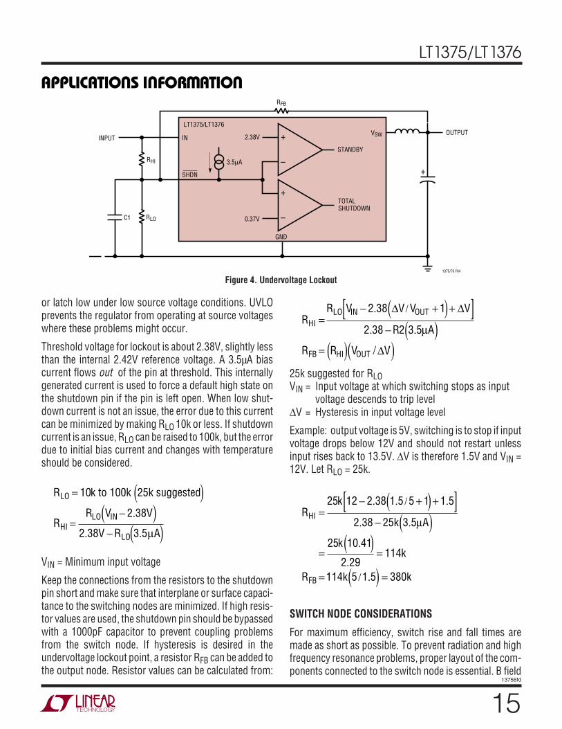
15
LT1375/LT1376
13756fd
APPLICATIONS INFORMATION
WU UU
–
+
–
+
2.38V
0.37V
GND
VSW
LT1375/LT1376
INPUT
RFB
RHI
1375/76 F04
OUTPUT
SHDN
STANDBY
IN
TOTALSHUTDOWN
3.5µA
RLOC1
+
Figure 4. Undervoltage Lockout
or latch low under low source voltage conditions. UVLOprevents the regulator from operating at source voltageswhere these problems might occur.
Threshold voltage for lockout is about 2.38V, slightly lessthan the internal 2.42V reference voltage. A 3.5µA biascurrent flows out of the pin at threshold. This internallygenerated current is used to force a default high state onthe shutdown pin if the pin is left open. When low shut-down current is not an issue, the error due to this currentcan be minimized by making RLO 10k or less. If shutdowncurrent is an issue, RLO can be raised to 100k, but the errordue to initial bias current and changes with temperatureshould be considered.
R k
RR V V
V R A
LO
HILO IN
LO
= ( )=
−( )− ( )
10
2 38
2 38 3 5
to 100k 25k suggested
.
. . µ
VIN = Minimum input voltage
Keep the connections from the resistors to the shutdownpin short and make sure that interplane or surface capaci-tance to the switching nodes are minimized. If high resis-tor values are used, the shutdown pin should be bypassedwith a 1000pF capacitor to prevent coupling problemsfrom the switch node. If hysteresis is desired in theundervoltage lockout point, a resistor RFB can be added tothe output node. Resistor values can be calculated from:
RR V V V V
R A
R R V V
HILO IN OUT
FB HI OUT
=− +( ) +[ ]
− ( )= ( )( )
2 38 1
2 38 2 3 5
. /
. .
/
∆ ∆
∆
µ
25k suggested for RLOVIN = Input voltage at which switching stops as input
voltage descends to trip level∆V = Hysteresis in input voltage level
Example: output voltage is 5V, switching is to stop if inputvoltage drops below 12V and should not restart unlessinput rises back to 13.5V. ∆V is therefore 1.5V and VIN =12V. Let RLO = 25k.
Rk
k A
kk
R k k
HI
FB
=− +( ) +[ ]
− ( )=
( )=
= ( ) =
25 12 2 38 1 5 5 1 1 5
2 38 25 3 5
25 10 41
2 29114
114 5 1 5 380
. . / .
. .
.
./ .
µ
SWITCH NODE CONSIDERATIONS
For maximum efficiency, switch rise and fall times aremade as short as possible. To prevent radiation and highfrequency resonance problems, proper layout of the com-ponents connected to the switch node is essential. B field
16
LT1375/LT1376
13756fd
APPLICATIONS INFORMATION
WU UU
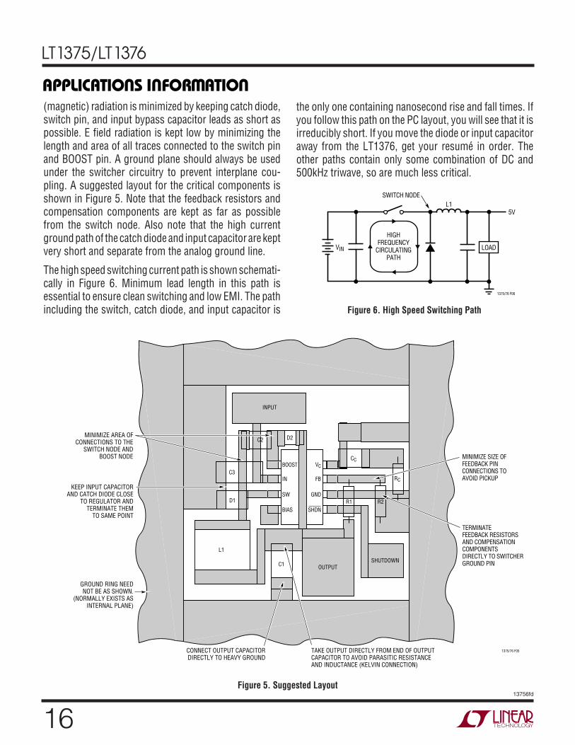
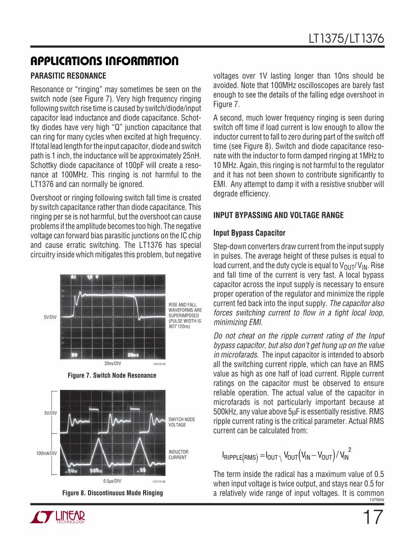
(magnetic) radiation is minimized by keeping catch diode,switch pin, and input bypass capacitor leads as short aspossible. E field radiation is kept low by minimizing thelength and area of all traces connected to the switch pinand BOOST pin. A ground plane should always be usedunder the switcher circuitry to prevent interplane cou-pling. A suggested layout for the critical components isshown in Figure 5. Note that the feedback resistors andcompensation components are kept as far as possiblefrom the switch node. Also note that the high currentground path of the catch diode and input capacitor are keptvery short and separate from the analog ground line.
The high speed switching current path is shown schemati-cally in Figure 6. Minimum lead length in this path isessential to ensure clean switching and low EMI. The pathincluding the switch, catch diode, and input capacitor is
the only one containing nanosecond rise and fall times. Ifyou follow this path on the PC layout, you will see that it isirreducibly short. If you move the diode or input capacitoraway from the LT1376, get your resumé in order. Theother paths contain only some combination of DC and500kHz triwave, so are much less critical.
Figure 5. Suggested Layout
INPUT
C2
C3
D2
CC
RC
R1
C1
1375/76 F05
D1
L1
R2
BOOST
IN
SW
BIAS
VC
FB
GND
SHDN
SHUTDOWNOUTPUT
MINIMIZE AREA OFCONNECTIONS TO THE
SWITCH NODE ANDBOOST NODE
KEEP INPUT CAPACITORAND CATCH DIODE CLOSE
TO REGULATOR ANDTERMINATE THEM
TO SAME POINT
CONNECT OUTPUT CAPACITORDIRECTLY TO HEAVY GROUND
TAKE OUTPUT DIRECTLY FROM END OF OUTPUTCAPACITOR TO AVOID PARASITIC RESISTANCEAND INDUCTANCE (KELVIN CONNECTION)
MINIMIZE SIZE OFFEEDBACK PINCONNECTIONS TOAVOID PICKUP
TERMINATEFEEDBACK RESISTORSAND COMPENSATIONCOMPONENTSDIRECTLY TO SWITCHERGROUND PIN
GROUND RING NEEDNOT BE AS SHOWN.
(NORMALLY EXISTS ASINTERNAL PLANE)
Figure 6. High Speed Switching Path
1375/76 F06
5VL1
VIN
HIGHFREQUENCY
CIRCULATINGPATH
LOAD
SWITCH NODE
17
LT1375/LT1376
13756fd
APPLICATIONS INFORMATION
WU UU
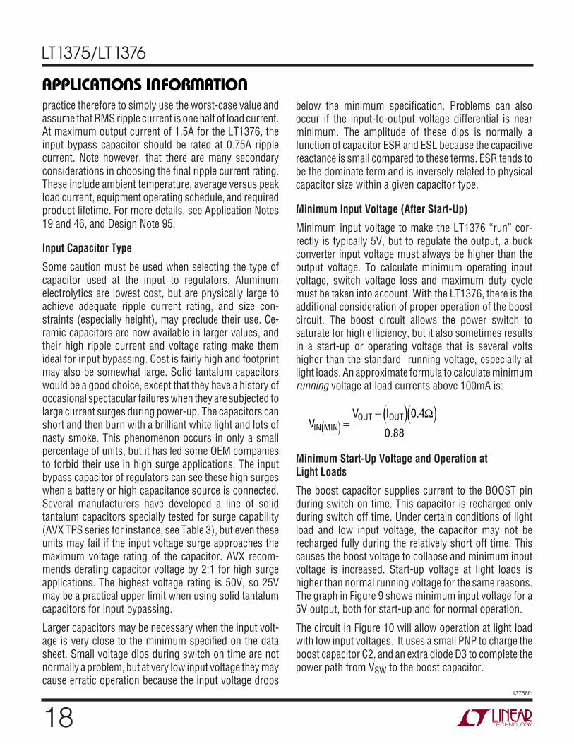
PARASITIC RESONANCE
Resonance or “ringing” may sometimes be seen on theswitch node (see Figure 7). Very high frequency ringingfollowing switch rise time is caused by switch/diode/inputcapacitor lead inductance and diode capacitance. Schot-tky diodes have very high “Q” junction capacitance thatcan ring for many cycles when excited at high frequency.If total lead length for the input capacitor, diode and switchpath is 1 inch, the inductance will be approximately 25nH.Schottky diode capacitance of 100pF will create a reso-nance at 100MHz. This ringing is not harmful to theLT1376 and can normally be ignored.
Overshoot or ringing following switch fall time is createdby switch capacitance rather than diode capacitance. Thisringing per se is not harmful, but the overshoot can causeproblems if the amplitude becomes too high. The negativevoltage can forward bias parasitic junctions on the IC chipand cause erratic switching. The LT1376 has specialcircuitry inside which mitigates this problem, but negative
voltages over 1V lasting longer than 10ns should beavoided. Note that 100MHz oscilloscopes are barely fastenough to see the details of the falling edge overshoot inFigure 7.
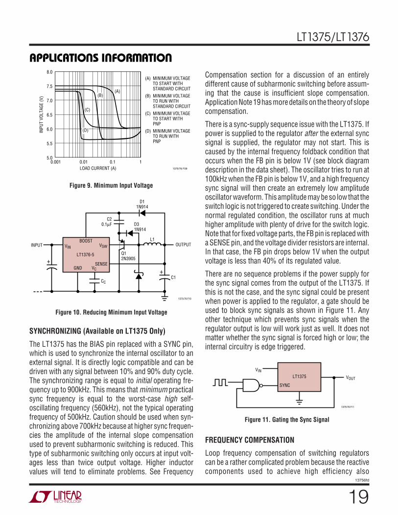
A second, much lower frequency ringing is seen duringswitch off time if load current is low enough to allow theinductor current to fall to zero during part of the switch offtime (see Figure 8). Switch and diode capacitance reso-nate with the inductor to form damped ringing at 1MHz to10 MHz. Again, this ringing is not harmful to the regulatorand it has not been shown to contribute significantly toEMI. Any attempt to damp it with a resistive snubber willdegrade efficiency.
INPUT BYPASSING AND VOLTAGE RANGE
Input Bypass Capacitor
Step-down converters draw current from the input supplyin pulses. The average height of these pulses is equal toload current, and the duty cycle is equal to VOUT/VIN. Riseand fall time of the current is very fast. A local bypasscapacitor across the input supply is necessary to ensureproper operation of the regulator and minimize the ripplecurrent fed back into the input supply. The capacitor alsoforces switching current to flow in a tight local loop,minimizing EMI.
Do not cheat on the ripple current rating of the Inputbypass capacitor, but also don’t get hung up on the valuein microfarads. The input capacitor is intended to absorball the switching current ripple, which can have an RMSvalue as high as one half of load current. Ripple currentratings on the capacitor must be observed to ensurereliable operation. The actual value of the capacitor inmicrofarads is not particularly important because at500kHz, any value above 5µF is essentially resistive. RMSripple current rating is the critical parameter. Actual RMScurrent can be calculated from:
I I V V V VRIPPLE RMS OUT OUT IN OUT IN( ) = −( ) / 2
The term inside the radical has a maximum value of 0.5when input voltage is twice output, and stays near 0.5 fora relatively wide range of input voltages. It is common
5V/DIV
Figure 7. Switch Node Resonance
20ns/DIV 1375/76 F07
20ns/DIV 1375/76 F11
0.5µs/DIV 1375/76 F08
Figure 8. Discontinuous Mode Ringing
5V/DIV
100mA/DIV
RISE AND FALLWAVEFORMS ARESUPERIMPOSED(PULSE WIDTH ISNOT 120ns)
SWITCH NODEVOLTAGE
INDUCTORCURRENT
18
LT1375/LT1376
13756fd
APPLICATIONS INFORMATION
WU UU
practice therefore to simply use the worst-case value andassume that RMS ripple current is one half of load current.At maximum output current of 1.5A for the LT1376, theinput bypass capacitor should be rated at 0.75A ripplecurrent. Note however, that there are many secondaryconsiderations in choosing the final ripple current rating.These include ambient temperature, average versus peakload current, equipment operating schedule, and requiredproduct lifetime. For more details, see Application Notes19 and 46, and Design Note 95.
Input Capacitor Type
Some caution must be used when selecting the type ofcapacitor used at the input to regulators. Aluminumelectrolytics are lowest cost, but are physically large toachieve adequate ripple current rating, and size con-straints (especially height), may preclude their use. Ce-ramic capacitors are now available in larger values, andtheir high ripple current and voltage rating make themideal for input bypassing. Cost is fairly high and footprintmay also be somewhat large. Solid tantalum capacitorswould be a good choice, except that they have a history ofoccasional spectacular failures when they are subjected tolarge current surges during power-up. The capacitors canshort and then burn with a brilliant white light and lots ofnasty smoke. This phenomenon occurs in only a smallpercentage of units, but it has led some OEM companiesto forbid their use in high surge applications. The inputbypass capacitor of regulators can see these high surgeswhen a battery or high capacitance source is connected.Several manufacturers have developed a line of solidtantalum capacitors specially tested for surge capability(AVX TPS series for instance, see Table 3), but even theseunits may fail if the input voltage surge approaches themaximum voltage rating of the capacitor. AVX recom-mends derating capacitor voltage by 2:1 for high surgeapplications. The highest voltage rating is 50V, so 25Vmay be a practical upper limit when using solid tantalumcapacitors for input bypassing.
Larger capacitors may be necessary when the input volt-age is very close to the minimum specified on the datasheet. Small voltage dips during switch on time are notnormally a problem, but at very low input voltage they maycause erratic operation because the input voltage drops
below the minimum specification. Problems can alsooccur if the input-to-output voltage differential is nearminimum. The amplitude of these dips is normally afunction of capacitor ESR and ESL because the capacitivereactance is small compared to these terms. ESR tends tobe the dominate term and is inversely related to physicalcapacitor size within a given capacitor type.
Minimum Input Voltage (After Start-Up)
Minimum input voltage to make the LT1376 “run” cor-rectly is typically 5V, but to regulate the output, a buckconverter input voltage must always be higher than theoutput voltage. To calculate minimum operating inputvoltage, switch voltage loss and maximum duty cyclemust be taken into account. With the LT1376, there is theadditional consideration of proper operation of the boostcircuit. The boost circuit allows the power switch tosaturate for high efficiency, but it also sometimes resultsin a start-up or operating voltage that is several voltshigher than the standard running voltage, especially atlight loads. An approximate formula to calculate minimumrunning voltage at load currents above 100mA is:
VV I
IN MINOUT OUT
( ) =+ ( )( )0 4
0 88
.
.
Ω
Minimum Start-Up Voltage and Operation atLight Loads
The boost capacitor supplies current to the BOOST pinduring switch on time. This capacitor is recharged onlyduring switch off time. Under certain conditions of lightload and low input voltage, the capacitor may not berecharged fully during the relatively short off time. Thiscauses the boost voltage to collapse and minimum inputvoltage is increased. Start-up voltage at light loads ishigher than normal running voltage for the same reasons.The graph in Figure 9 shows minimum input voltage for a5V output, both for start-up and for normal operation.
The circuit in Figure 10 will allow operation at light loadwith low input voltages. It uses a small PNP to charge theboost capacitor C2, and an extra diode D3 to complete thepower path from VSW to the boost capacitor.
19
LT1375/LT1376
13756fd
APPLICATIONS INFORMATION
WU UU
LOAD CURRENT (A)0.001
INPU
T VO
LTAG
E (V
)
8.0
7.5
7.0
6.5
6.0
5.5
5.00.01 0.1 1
1375/76 F09
(A)
(C)
(D)
(A) MINIMUM VOLTAGETO START WITHSTANDARD CIRCUIT
(B) MINIMUM VOLTAGETO RUN WITHSTANDARD CIRCUIT
(C) MINIMUM VOLTAGETO START WITHPNP
(D) MINIMUM VOLTAGETO RUN WITHPNP
(B)
Figure 9. Minimum Input Voltage
Figure 10. Reducing Minimum Input Voltage
OUTPUTINPUT
1375/76 F10
C20.1µF
CC
D31N914
Q12N3905
C1
D11N914
L1BOOST
LT1376-5
VIN VSW
SENSEGND VC
+
+
Compensation section for a discussion of an entirelydifferent cause of subharmonic switching before assum-ing that the cause is insufficient slope compensation.Application Note 19 has more details on the theory of slopecompensation.
There is a sync-supply sequence issue with the LT1375. Ifpower is supplied to the regulator after the external syncsignal is supplied, the regulator may not start. This iscaused by the internal frequency foldback condition thatoccurs when the FB pin is below 1V (see block diagramdescription in the data sheet). The oscillator tries to run at100kHz when the FB pin is below 1V, and a high frequencysync signal will then create an extremely low amplitudeoscillator waveform. This amplitude may be so low that theswitch logic is not triggered to create switching. Under thenormal regulated condition, the oscillator runs at muchhigher amplitude with plenty of drive for the switch logic.Note that for fixed voltage parts, the FB pin is replaced witha SENSE pin, and the voltage divider resistors are internal.In that case, the FB pin drops below 1V when the outputvoltage is less than 40% of its regulated value.
There are no sequence problems if the power supply forthe sync signal comes from the output of the LT1375. Ifthis is not the case, and the sync signal could be presentwhen power is applied to the regulator, a gate should beused to block sync signals as shown in Figure 11. Anyother technique which prevents sync signals when theregulator output is low will work just as well. It does notmatter whether the sync signal is forced high or low; theinternal circuitry is edge triggered.
SYNCHRONIZING (Available on LT1375 Only)
The LT1375 has the BIAS pin replaced with a SYNC pin,which is used to synchronize the internal oscillator to anexternal signal. It is directly logic compatible and can bedriven with any signal between 10% and 90% duty cycle.The synchronizing range is equal to initial operating fre-quency up to 900kHz. This means that minimum practicalsync frequency is equal to the worst-case high self-oscillating frequency (560kHz), not the typical operatingfrequency of 500kHz. Caution should be used when syn-chronizing above 700kHz because at higher sync frequen-cies the amplitude of the internal slope compensationused to prevent subharmonic switching is reduced. Thistype of subharmonic switching only occurs at input volt-ages less than twice output voltage. Higher inductorvalues will tend to eliminate problems. See Frequency
LT1375
SYNC
VOUT
1375/76 F11
VIN
FREQUENCY COMPENSATION
Loop frequency compensation of switching regulatorscan be a rather complicated problem because the reactivecomponents used to achieve high efficiency also
Figure 11. Gating the Sync Signal
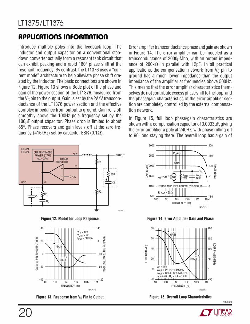
20
LT1375/LT1376
13756fd
APPLICATIONS INFORMATION
WU UU
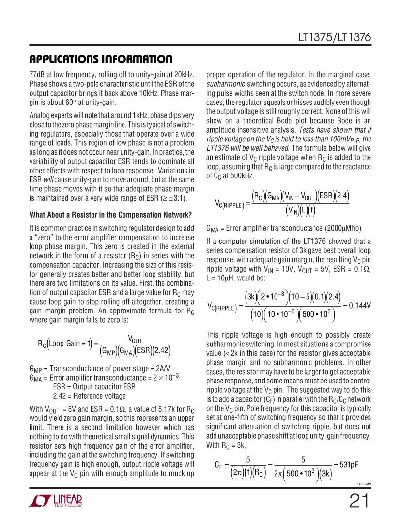
Error amplifier transconductance phase and gain are shownin Figure 14. The error amplifier can be modeled as atransconductance of 2000µMho, with an output imped-ance of 200kΩ in parallel with 12pF. In all practicalapplications, the compensation network from VC pin toground has a much lower impedance than the outputimpedance of the amplifier at frequencies above 500Hz.This means that the error amplifier characteristics them-selves do not contribute excess phase shift to the loop, andthe phase/gain characteristics of the error amplifier sec-tion are completely controlled by the external compensa-tion network.
In Figure 15, full loop phase/gain characteristics areshown with a compensation capacitor of 0.0033µF, givingthe error amplifier a pole at 240Hz, with phase rolling offto 90° and staying there. The overall loop has a gain of
introduce multiple poles into the feedback loop. Theinductor and output capacitor on a conventional step-down converter actually form a resonant tank circuit thatcan exhibit peaking and a rapid 180° phase shift at theresonant frequency. By contrast, the LT1376 uses a “cur-rent mode” architecture to help alleviate phase shift cre-ated by the inductor. The basic connections are shown inFigure 12. Figure 13 shows a Bode plot of the phase andgain of the power section of the LT1376, measured fromthe VC pin to the output. Gain is set by the 2A/V transcon-ductance of the LT1376 power section and the effectivecomplex impedance from output to ground. Gain rolls offsmoothly above the 100Hz pole frequency set by the100µF output capacitor. Phase drop is limited to about85°. Phase recovers and gain levels off at the zero fre-quency (≈16kHz) set by capacitor ESR (0.1Ω).
Figure 13. Response from VC Pin to Output Figure 15. Overall Loop Characteristics
FREQUENCY (Hz)
GAIN
: VC
PIN
TO O
UTPU
T (d
B)
PHASE: VC PIN TO OUTPUT (DEG)
40
20
0
–20
–40
40
0
–40
–80
–12010 1k 10k 1M
1375/76 F13
100 100k
GAIN
PHASE
VIN = 10VVOUT = 5VIOUT = 500mA
FREQUENCY (Hz)
LOOP
GAI
N (d
B)
LOOP PHASE (DEG)
80
60
40
20
0
–20
200
150
100
50
0
–5010 1k 10k 1M
1375/76 F15
100 100k
GAIN
PHASE
VIN = 10VVOUT = 5V, IOUT = 500mACOUT = 100µF, 10V, AVX TPSCC = 3.3nF, RC = 0, L = 10µH
Figure 12. Model for Loop Response Figure 14. Error Amplifier Gain and Phase
–
+
2.42V
VSW
VC
LT1375LT1376
GND
1375/76 F12
R1
OUTPUT
ESR
CF
CC
RC
ERRORAMPLIFIER
FB
+
R2
C1
CURRENT MODEPOWER STAGE
gm = 2A/V
FREQUENCY (Hz)
GAIN
(µM
ho) PHASE (DEG)
3000
2500
2000
1500
1000
500
200
150
100
50
0
–50100 10k 100k 10M
1375/76 F14
1k 1M
GAIN
PHASE
ROUT200k
COUT12pF
VC
ERROR AMPLIFIER EQUIVALENT CIRCUIT
RLOAD = 50Ω
VFB 2 • 10–3 )(
21
LT1375/LT1376
13756fd
APPLICATIONS INFORMATION
WU UU
77dB at low frequency, rolling off to unity-gain at 20kHz.Phase shows a two-pole characteristic until the ESR of theoutput capacitor brings it back above 10kHz. Phase mar-gin is about 60° at unity-gain.
Analog experts will note that around 1kHz, phase dips veryclose to the zero phase margin line. This is typical of switch-ing regulators, especially those that operate over a widerange of loads. This region of low phase is not a problemas long as it does not occur near unity-gain. In practice, thevariability of output capacitor ESR tends to dominate allother effects with respect to loop response. Variations inESR will cause unity-gain to move around, but at the sametime phase moves with it so that adequate phase marginis maintained over a very wide range of ESR (≥ ±3:1).
What About a Resistor in the Compensation Network?
It is common practice in switching regulator design to adda “zero” to the error amplifier compensation to increaseloop phase margin. This zero is created in the externalnetwork in the form of a resistor (RC) in series with thecompensation capacitor. Increasing the size of this resis-tor generally creates better and better loop stability, butthere are two limitations on its value. First, the combina-tion of output capacitor ESR and a large value for RC maycause loop gain to stop rolling off altogether, creating again margin problem. An approximate formula for RCwhere gain margin falls to zero is:
R LoopV
G G ESRC
OUT
MP MA
Gain = 1( ) = ( )( )( )( )2 42.
GMP = Transconductance of power stage = 2A/VGMA = Error amplifier transconductance = 2 × 10⁻³
ESR = Output capacitor ESR2.42 = Reference voltage
With VOUT = 5V and ESR = 0.1Ω, a value of 5.17k for RCwould yield zero gain margin, so this represents an upperlimit. There is a second limitation however which hasnothing to do with theoretical small signal dynamics. Thisresistor sets high frequency gain of the error amplifier,including the gain at the switching frequency. If switchingfrequency gain is high enough, output ripple voltage willappear at the VC pin with enough amplitude to muck up
proper operation of the regulator. In the marginal case,subharmonic switching occurs, as evidenced by alternat-ing pulse widths seen at the switch node. In more severecases, the regulator squeals or hisses audibly even thoughthe output voltage is still roughly correct. None of this willshow on a theoretical Bode plot because Bode is anamplitude insensitive analysis. Tests have shown that ifripple voltage on the VC is held to less than 100mVP-P, theLT1376 will be well behaved. The formula below will givean estimate of VC ripple voltage when RC is added to theloop, assuming that RC is large compared to the reactanceof CC at 500kHz.
VR G V V ESR
V L fC RIPPLE
C MA IN OUT
IN( ) =
( )( ) −( )( )( )( )( )( )
2 4.
GMA = Error amplifier transconductance (2000µMho)
If a computer simulation of the LT1376 showed that aseries compensation resistor of 3k gave best overall loopresponse, with adequate gain margin, the resulting VC pinripple voltage with VIN = 10V, VOUT = 5V, ESR = 0.1Ω,L = 10µH, would be:
Vk
VC RIPPLE( )−
−=
( )⎛⎝ ⎞⎠ −( )( )( )
( )⎛⎝ ⎞⎠⎛⎝
⎞⎠
=3 2 10 10 5 0 1 2 4
10 10 10 500 100 144
3
6 3
• . .
• •.
This ripple voltage is high enough to possibly createsubharmonic switching. In most situations a compromisevalue (<2k in this case) for the resistor gives acceptablephase margin and no subharmonic problems. In othercases, the resistor may have to be larger to get acceptablephase response, and some means must be used to controlripple voltage at the VC pin. The suggested way to do thisis to add a capacitor (CF) in parallel with the RC/CC networkon the VC pin. Pole frequency for this capacitor is typicallyset at one-fifth of switching frequency so that it providessignificant attenuation of switching ripple, but does notadd unacceptable phase shift at loop unity-gain frequency.With RC = 3k,
Cf R k
pFFC
= ( )( )( ) =⎛⎝
⎞⎠ ( )
=5
2
5
2 500 10 3531
3π π •
22
LT1375/LT1376
13756fd
APPLICATIONS INFORMATION
WU UU
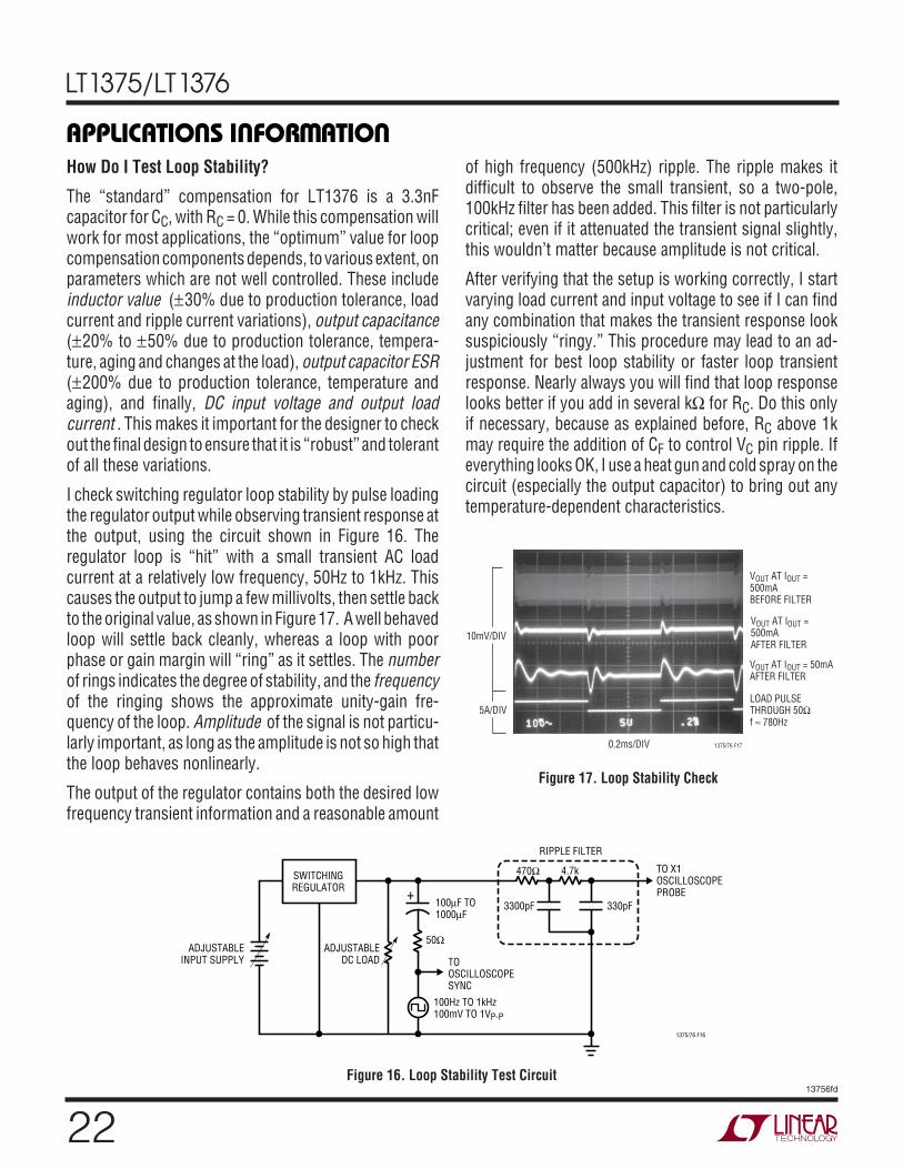
How Do I Test Loop Stability?
The “standard” compensation for LT1376 is a 3.3nFcapacitor for CC, with RC = 0. While this compensation willwork for most applications, the “optimum” value for loopcompensation components depends, to various extent, onparameters which are not well controlled. These includeinductor value (±30% due to production tolerance, loadcurrent and ripple current variations), output capacitance(±20% to ±50% due to production tolerance, tempera-ture, aging and changes at the load), output capacitor ESR(±200% due to production tolerance, temperature andaging), and finally, DC input voltage and output loadcurrent . This makes it important for the designer to checkout the final design to ensure that it is “robust” and tolerantof all these variations.
I check switching regulator loop stability by pulse loadingthe regulator output while observing transient response atthe output, using the circuit shown in Figure 16. Theregulator loop is “hit” with a small transient AC loadcurrent at a relatively low frequency, 50Hz to 1kHz. Thiscauses the output to jump a few millivolts, then settle backto the original value, as shown in Figure 17. A well behavedloop will settle back cleanly, whereas a loop with poorphase or gain margin will “ring” as it settles. The numberof rings indicates the degree of stability, and the frequencyof the ringing shows the approximate unity-gain fre-quency of the loop. Amplitude of the signal is not particu-larly important, as long as the amplitude is not so high thatthe loop behaves nonlinearly.
The output of the regulator contains both the desired lowfrequency transient information and a reasonable amount
of high frequency (500kHz) ripple. The ripple makes itdifficult to observe the small transient, so a two-pole,100kHz filter has been added. This filter is not particularlycritical; even if it attenuated the transient signal slightly,this wouldn’t matter because amplitude is not critical.
After verifying that the setup is working correctly, I startvarying load current and input voltage to see if I can findany combination that makes the transient response looksuspiciously “ringy.” This procedure may lead to an ad-justment for best loop stability or faster loop transientresponse. Nearly always you will find that loop responselooks better if you add in several kΩ for RC. Do this onlyif necessary, because as explained before, RC above 1kmay require the addition of CF to control VC pin ripple. Ifeverything looks OK, I use a heat gun and cold spray on thecircuit (especially the output capacitor) to bring out anytemperature-dependent characteristics.
Figure 16. Loop Stability Test Circuit
TO OSCILLOSCOPESYNC
ADJUSTABLEDC LOAD
ADJUSTABLEINPUT SUPPLY
100Hz TO 1kHz100mV TO 1VP-P
100µF TO1000µF
RIPPLE FILTER
1375/76 F16
TO X1OSCILLOSCOPEPROBE
3300pF 330pF
50Ω
470Ω 4.7kSWITCHINGREGULATOR +
0.2ms/DIV 1375/76 F17
10mV/DIV
VOUT AT IOUT =500mABEFORE FILTER
VOUT AT IOUT =500mAAFTER FILTER
VOUT AT IOUT = 50mAAFTER FILTER
LOAD PULSETHROUGH 50Ωf ≈ 780Hz
5A/DIV
Figure 17. Loop Stability Check
23
LT1375/LT1376
13756fd
APPLICATIONS INFORMATION
WU UU
Keep in mind that this procedure does not take initialcomponent tolerance into account. You should see fairlyclean response under all load and line conditions to ensurethat component variations will not cause problems. Onenote here: according to Murphy, the component mostlikely to be changed in production is the output capacitor,because that is the component most likely to have manu-facturer variations (in ESR) large enough to cause prob-lems. It would be a wise move to lock down the sources ofthe output capacitor in production.
A possible exception to the “clean response” rule is at verylight loads, as evidenced in Figure 17 with ILOAD = 50mA.Switching regulators tend to have dramatic shifts in loopresponse at very light loads, mostly because the inductorcurrent becomes discontinuous. One common result isvery slow but stable characteristics. A second possibilityis low phase margin, as evidenced by ringing at the outputwith transients. The good news is that the low phasemargin at light loads is not particularly sensitive to com-ponent variation, so if it looks reasonable under a transienttest, it will probably not be a problem in production. Notethat frequency of the light load ringing may vary withcomponent tolerance but phase margin generally hangs inthere.
THERMAL CALCULATIONS
Power dissipation in the LT1376 chip comes from foursources: switch DC loss, switch AC loss, boost circuitcurrent, and input quiescent current. The following formu-las show how to calculate each of these losses. Theseformulas assume continuous mode operation, so theyshould not be used for calculating efficiency at light loadcurrents.
Switch loss:
PR I V
Vns I V fSW
SW OUT OUT
INOUT IN=
( ) ( )+ ( )( )( )
2
16
Boost current loss:
PV I
VBOOSTOUT OUT
IN=
+( )20 008 75. /
Quiescent current loss:
P V VV
VQ IN OUT
OUT
IN= ( ) + ( ) +
⎛⎝⎜
⎞⎠⎟( )
0 001 0 0050 002
2
. ..
RSW = Switch resistance (≈0.4)16ns = Equivalent switch current/voltage overlap timef = Switch frequencyExample: with VIN = 10V, VOUT = 5V and IOUT = 1A:
P
W
P W
P W
SW
BOOST
Q
=( )( ) ( )
+ ⎛⎝
⎞⎠ ( )( )⎛⎝ ⎞
⎠= + =
=( ) +( )
=
= ( ) + ( ) +( ) ( )
=
−0 4 1 5
1016 10 1 10 500 10
0 2 0 08 0 28
5 0 008 1 75
100 053
10 0 001 5 0 0055 0 002
100 04
2
9 3
2
2
.• •
. . .
. /.
. ..
.
Total power dissipation is 0.28 + 0.053 + 0.04 = 0.37W.
Thermal resistance for LT1376 package is influenced bythe presence of internal or backside planes. With a fullplane under the SO package, thermal resistance will beabout 120°C/W. No plane will increase resistance to about160°C/W. To calculate die temperature, use the properthermal resistance number for the desired package andadd in worst-case ambient temperature:
TJ = TA + θJA (PTOT)
With the SO-8 package (θJA = 120°C/W), at an ambienttemperature of 70°C,
TJ = 70 + 120 (0.37) = 114.4°C
Die temperature is highest at low input voltage, so uselowest continuous input operating voltage for thermalcalculations.
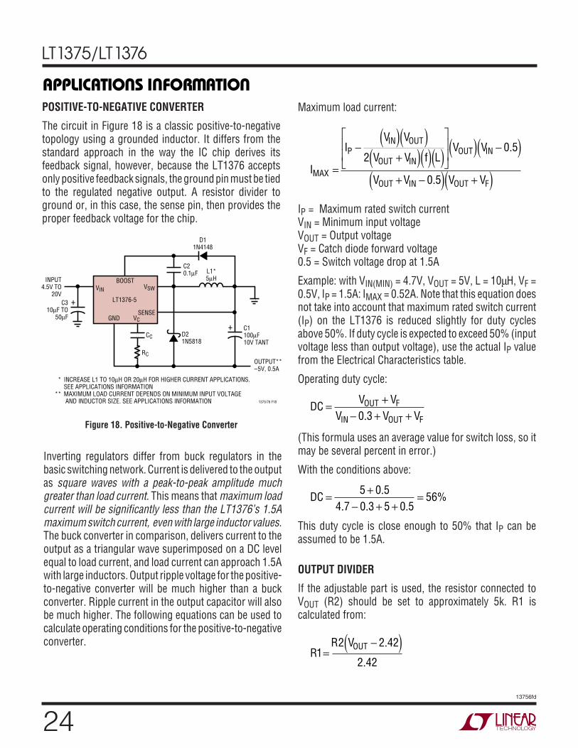
24
LT1375/LT1376
13756fd
APPLICATIONS INFORMATION
WU UU
POSITIVE-TO-NEGATIVE CONVERTER
The circuit in Figure 18 is a classic positive-to-negativetopology using a grounded inductor. It differs from thestandard approach in the way the IC chip derives itsfeedback signal, however, because the LT1376 acceptsonly positive feedback signals, the ground pin must be tiedto the regulated negative output. A resistor divider toground or, in this case, the sense pin, then provides theproper feedback voltage for the chip.
OUTPUT**–5V, 0.5A
INPUT4.5V TO
20V
1375/76 F18
C20.1µF
CC
RC
D21N5818
C1100µF10V TANT
C310µF TO
50µF
D11N4148
L1*5µHBOOST
LT1376-5
VIN VSW
SENSEGND VC
* INCREASE L1 TO 10µH OR 20µH FOR HIGHER CURRENT APPLICATIONS. SEE APPLICATIONS INFORMATION
** MAXIMUM LOAD CURRENT DEPENDS ON MINIMUM INPUT VOLTAGE AND INDUCTOR SIZE. SEE APPLICATIONS INFORMATION
+
+
Figure 18. Positive-to-Negative Converter
Inverting regulators differ from buck regulators in thebasic switching network. Current is delivered to the outputas square waves with a peak-to-peak amplitude muchgreater than load current. This means that maximum loadcurrent will be significantly less than the LT1376’s 1.5Amaximum switch current, even with large inductor values.The buck converter in comparison, delivers current to theoutput as a triangular wave superimposed on a DC levelequal to load current, and load current can approach 1.5Awith large inductors. Output ripple voltage for the positive-to-negative converter will be much higher than a buckconverter. Ripple current in the output capacitor will alsobe much higher. The following equations can be used tocalculate operating conditions for the positive-to-negativeconverter.
Maximum load current:
I
IV V
V V f LV V
V V V VMAX
PIN OUT
OUT INOUT IN
OUT IN OUT F
=
−( )( )
+( )( )( )⎡
⎣
⎢⎢
⎤
⎦
⎥⎥( ) −( )
+ −( ) +( )2
0 5
0 5
.
.
IP = Maximum rated switch currentVIN = Minimum input voltageVOUT = Output voltageVF = Catch diode forward voltage0.5 = Switch voltage drop at 1.5A
Example: with VIN(MIN) = 4.7V, VOUT = 5V, L = 10µH, VF =0.5V, IP = 1.5A: IMAX = 0.52A. Note that this equation doesnot take into account that maximum rated switch current(IP) on the LT1376 is reduced slightly for duty cyclesabove 50%. If duty cycle is expected to exceed 50% (inputvoltage less than output voltage), use the actual IP valuefrom the Electrical Characteristics table.
Operating duty cycle:
DCV V
V V VOUT F
IN OUT F= +
− + +0 3.
(This formula uses an average value for switch loss, so itmay be several percent in error.)
With the conditions above:
DC = +− + +
=5 0 54 7 0 3 5 0 5
56.
. . .%
This duty cycle is close enough to 50% that IP can beassumed to be 1.5A.
OUTPUT DIVIDER
If the adjustable part is used, the resistor connected toVOUT (R2) should be set to approximately 5k. R1 iscalculated from:
RR VOUT
12 2 42
2 42=
−( ).
.

25
LT1375/LT1376
13756fd
APPLICATIONS INFORMATION
WU UU
INDUCTOR VALUE
Unlike buck converters, positive-to-negative converterscannot use large inductor values to reduce output ripplevoltage. At 500kHz, values larger than 25µH make almostno change in output ripple. The graph in Figure 19 showspeak-to-peak output ripple voltage for a 5V to –5V con-verter versus inductor value. The criteria for choosing theinductor is therefore typically based on ensuring that peakswitch current rating is not exceeded. This gives thelowest value of inductance that can be used, but in somecases (lower output load currents) it may give a value thatcreates unnecessarily high output ripple voltage. A com-promise value is often chosen that reduces output ripple.As you can see from the graph, large inductors will notgive arbitrarily low ripple, but small inductors can givehigh ripple.
INDUCTOR SIZE (µH)0
OUTP
UT R
IPPL
E VO
LTAG
E (m
V P-P
)
150
120
90
60
30
020
1375/76 F19
5 10 15 25
5V TO –5V CONVERTEROUTPUT CAPACITORESR = 0.1Ω
ILOAD = 0.25A
ILOAD = 0.1A
Figure 19. Ripple Voltage on Positive-to-Negative Converter
The difficulty in calculating the minimum inductor sizeneeded is that you must first know whether the switcherwill be in continuous or discontinuous mode at the criticalpoint where switch current is 1.5A. The first step is to usethe following formula to calculate the load current wherethe switcher must use continuous mode. If your loadcurrent is less than this, use the discontinuous modeformula to calculate minimum inductor needed. If loadcurrent is higher, use the continuous mode formula.Output current where continuous mode is needed:
IV I
V V V V VCONT
IN P
IN OUT IN OUT F
=( ) ( )
+( ) + +( )2 2
4
Minimum inductor discontinuous mode:
LV I
f IMIN
OUT OUT
P
=( )( )
( )( )2
2
Minimum inductor continuous mode:
LV V
f V V I IV V
V
MININ OUT
IN OUT P OUTOUT F
IN
=( )( )
( ) +( ) − ++( )⎛
⎝⎜⎜
⎞
⎠⎟⎟
⎡
⎣
⎢⎢
⎤
⎦
⎥⎥
2 1
For the example above, with maximum load current of0.25A:
I ACONT =( ) ( )
+( ) + +( ) =5 1 5
4 5 5 5 5 0 50 37
2 2.
..
This says that discontinuous mode can be used and theminimum inductor needed is found from:
L HMIN =( )( )
⎛⎝
⎞⎠( )
=2 5 0 25
500 10 1 52 2
3 2
.
• .. µ
In practice, the inductor should be increased by about30% over the calculated minimum to handle losses andvariations in value. This suggests a minimum inductor of3µH for this application, but looking at the ripple voltagechart shows that output ripple voltage could be reduced bya factor of two by using a 15µH inductor. There is no ruleof thumb here to make a final decision. If modest ripple isneeded and the larger inductor does the trick, go for it. Ifripple is noncritical use the smaller inductor. If ripple isextremely critical, a second filter may have to be added inany case, and the lower value of inductance can be used.Keep in mind that the output capacitor is the other criticalfactor in determining output ripple voltage. Ripple shownon the graph (Figure 19) is with a capacitor ESR of 0.1Ω.This is reasonable for an AVX type TPS “D” or “E” size
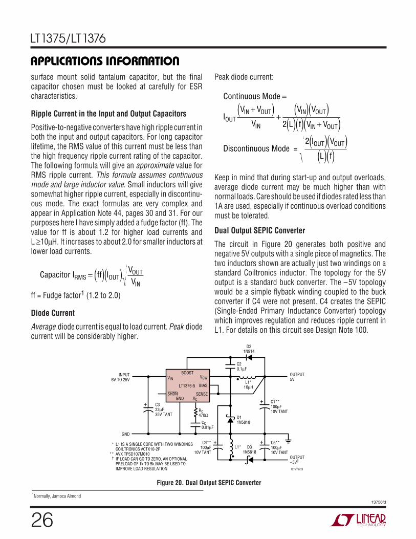
26
LT1375/LT1376
13756fd
APPLICATIONS INFORMATION
WU UU
surface mount solid tantalum capacitor, but the finalcapacitor chosen must be looked at carefully for ESRcharacteristics.
Ripple Current in the Input and Output Capacitors
Positive-to-negative converters have high ripple current inboth the input and output capacitors. For long capacitorlifetime, the RMS value of this current must be less thanthe high frequency ripple current rating of the capacitor.The following formula will give an approximate value forRMS ripple current. This formula assumes continuousmode and large inductor value. Small inductors will givesomewhat higher ripple current, especially in discontinu-ous mode. The exact formulas are very complex andappear in Application Note 44, pages 30 and 31. For ourpurposes here I have simply added a fudge factor (ff). Thevalue for ff is about 1.2 for higher load currents andL ≥10µH. It increases to about 2.0 for smaller inductors atlower load currents.
Capacitor ff IVVOUTOUT
IN IRMS = ( )( )
ff = Fudge factor1 (1.2 to 2.0)
Diode Current
Average diode current is equal to load current. Peak diodecurrent will be considerably higher.
1Normally, Jamoca Almond
Peak diode current:
Continuous
IV V
V
V V
L f V V
DiscontinuousV
L f
OUTIN OUT
IN
IN OUT
IN OUT
OUT
Mode
Mode =2 IOUT
=+( )
+( )( )
( )( ) +( )( )( )
( )( )
2
Keep in mind that during start-up and output overloads,average diode current may be much higher than withnormal loads. Care should be used if diodes rated less than1A are used, especially if continuous overload conditionsmust be tolerated.
Dual Output SEPIC Converter
The circuit in Figure 20 generates both positive andnegative 5V outputs with a single piece of magnetics. Thetwo inductors shown are actually just two windings on astandard Coiltronics inductor. The topology for the 5Voutput is a standard buck converter. The –5V topologywould be a simple flyback winding coupled to the buckconverter if C4 were not present. C4 creates the SEPIC(Single-Ended Primary Inductance Converter) topologywhich improves regulation and reduces ripple current inL1. For details on this circuit see Design Note 100.
BOOST
LT1376-5
VINOUTPUT5V
OUTPUT–5V†
* L1 IS A SINGLE CORE WITH TWO WINDINGSCOILTRONICS #CTX10-2P
** AVX TPSD107M010† IF LOAD CAN GO TO ZERO, AN OPTIONAL
PRELOAD OF 1k TO 5k MAY BE USED TOIMPROVE LOAD REGULATION
INPUT6V TO 25V
GND
1375/76 F20
C20.1µF
CC0.01µF
RC470Ω D1
1N5818
C1**100µF10V TANT
C5**100µF10V TANT
C322µF35V TANT
C4**100µF
10V TANT
D21N914
D31N5818
L1*10µH
L1*
VSW
SENSE
BIAS
GNDSHDN
VC+ +
+ +
Figure 20. Dual Output SEPIC Converter
27
LT1375/LT1376
13756fd
N8 1002
.065(1.651)
TYP
.045 – .065(1.143 – 1.651)
.130 ± .005(3.302 ± 0.127)
.020(0.508)
MIN.018 ± .003(0.457 ± 0.076)
.120(3.048)
MIN
1 2 3 4
8 7 6 5
.255 ± .015*(6.477 ± 0.381)
.400*(10.160)
MAX
.008 – .015(0.203 – 0.381)
.300 – .325(7.620 – 8.255)
.325+.035–.015+0.889–0.3818.255( )
NOTE:1. DIMENSIONS ARE
INCHESMILLIMETERS
*THESE DIMENSIONS DO NOT INCLUDE MOLD FLASH OR PROTRUSIONS. MOLD FLASH OR PROTRUSIONS SHALL NOT EXCEED .010 INCH (0.254mm)
.100(2.54)BSC
Information furnished by Linear Technology Corporation is believed to be accurate and reliable.However, no responsibility is assumed for its use. Linear Technology Corporation makes no represen-tation that the interconnection of its circuits as described herein will not infringe on existing patent rights.
PACKAGE DESCRIPTION
U
N8 Package8-Lead PDIP (Narrow 0.300)
(LTC DWG # 05-08-1510)
S8 Package8-Lead Plastic Small Outline (Narrow 0.150)
(LTC DWG # 05-08-1610)
.016 – .050(0.406 – 1.270)
.010 – .020(0.254 – 0.508)
× 45°
0°– 8° TYP.008 – .010
(0.203 – 0.254)
SO8 0303
.053 – .069(1.346 – 1.752)
.014 – .019(0.355 – 0.483)
TYP
.004 – .010(0.101 – 0.254)
.050(1.270)
BSC
1 2 3 4
.150 – .157(3.810 – 3.988)
NOTE 3
8 7 6 5
.189 – .197(4.801 – 5.004)
NOTE 3
.228 – .244(5.791 – 6.197)
.245MIN .160 ±.005
RECOMMENDED SOLDER PAD LAYOUT
.045 ±.005 .050 BSC
.030 ±.005 TYP
INCHES(MILLIMETERS)
NOTE:1. DIMENSIONS IN
2. DRAWING NOT TO SCALE3. THESE DIMENSIONS DO NOT INCLUDE MOLD FLASH OR PROTRUSIONS. MOLD FLASH OR PROTRUSIONS SHALL NOT EXCEED .006" (0.15mm)

28
LT1375/LT1376
13756fd
RELATED PARTSPART NUMBER DESCRIPTION COMMENTS
LT1370 High Efficiency DC/DC Converter 42V, 6A, 500kHz Switch
LT1371 High Efficiency DC/DC Converter 35V, 3A, 500kHz Switch
LT1372/LT1377 500kHz and 1MHz High Efficiency 1.5A Switching Regulators Boost Topology
LT1374 High Efficiency Step-Down Switching Regulator 25V, 4.5A, 500kHz Switch
LT1375/LT1376 1.5A Step-Down Switching Regulators 500kHz, Synchronizable in SO-8 Package
LT1507 1.5A Step-Down Switching Regulator 500kHz, 4V to 16V Input, SO-8 Package
LT1576 1.5A Step-Down Switching Regulator 200kHz, Reduced EMI Generation
LT1578 1.5A Step-Down Switching Regulator 200kHz, Reduced EMI Generation
LT1616 600mA Step-Down Switching Regulator 1.4MHz, 4V to 25V Input, SOT-23 Package
LT1676/LT1776 Wide Input Range Step-Down Switching Regulators 60V Input, 700mA Internal Switches
LTC1735 High Efficiency Synchronous Step-Down, N-Ch Drive Burst Mode® Operation, 16-Pin Narrow SSOP
LTC1735-1 High Efficiency Step-Down Controller with Power Good Output Fault Protection, 16-Pin SSOP and SO-8
LT1767 1.5A, 1.4MHz Step-Down DC/DC Converter Higher Current, 8-Lead MSOP Package
LTC1772 Constant Frequency Step-Down Controller in SOT-23 Higher Current, High Effieciency: Up to 94%
LTC1779 0.25A Micropower Step-Down in SOT-23 Lower Current, 100% Duty Cycle
LTC1877 High Efficiency Monolithic Step-Down Regulator 550kHz, MS8, VIN Up to 10V, IQ =10µA, IOUT to 600mA at VIN = 5V
LTC1878 High Efficiency Monolithic Step-Down Regulator 550kHz, MS8, VIN Up to 6V, IQ = 10µA, IOUT to 600mA at VIN = 3.3V
LTC3404 1.4MHz High Efficiency, Monolithic Synchronous Step-Down Up to 95% Efficiency, 100% Duty Cycle, IQ = 10µA,Regulator VIN = 2.65V to 6V
Burst Mode is a registered trademark of Linear Technology Corporation.
LT 0306 REV D • PRINTED IN USA
© LINEAR TECHNOLOGY CORPORATION 1995
PACKAGE DESCRIPTION
U
S Package16-Lead Plastic Small Outline (Narrow 0.150)
(LTC DWG # 05-08-1610)
Linear Technology Corporation1630 McCarthy Blvd., Milpitas, CA 95035-7417(408) 432-1900 FAX: (408) 434-0507 www.linear.com
.016 – .050(0.406 – 1.270)
.010 – .020(0.254 – 0.508)
× 45°
0° – 8° TYP.008 – .010
(0.203 – 0.254)
1
N
2 3 4 5 6 7 8
N/2
.150 – .157(3.810 – 3.988)
NOTE 3
16 15 14 13
.386 – .394(9.804 – 10.008)
NOTE 3
.228 – .244(5.791 – 6.197)
12 11 10 9
S16 0502
.053 – .069(1.346 – 1.752)
.014 – .019(0.355 – 0.483)
TYP
.004 – .010(0.101 – 0.254)
.050(1.270)
BSC
.245MIN
N
1 2 3 N/2
.160 ±.005
RECOMMENDED SOLDER PAD LAYOUT
.045 ±.005 .050 BSC
.030 ±.005 TYP
INCHES(MILLIMETERS)
NOTE:1. DIMENSIONS IN
2. DRAWING NOT TO SCALE3. THESE DIMENSIONS DO NOT INCLUDE MOLD FLASH OR PROTRUSIONS. MOLD FLASH OR PROTRUSIONS SHALL NOT EXCEED .006" (0.15mm)