LT1054 Switched-Capacitor Voltage Converters With ... · LT1054 SLVS033G –FEBRUARY 1990–REVISED...
35
-V OUT V IN LT1054 V OUT V REF OSC V CC CAP- GND CAP+ FB/SD 10 F μ + 1 2 3 4 8 7 6 5 + + 2 μF 100 μF Product Folder Sample & Buy Technical Documents Tools & Software Support & Community LT1054 SLVS033G – FEBRUARY 1990 – REVISED JULY 2015 LT1054 Switched-Capacitor Voltage Converters With Regulators 1 Features 3 Description The LT1054 device is a bipolar, switched-capacitor 1• Output Current, 100 mA voltage converter with regulator. It provides higher • Low Loss, 1.1 V at 100 mA output current and significantly lower voltage losses • Operating Range, 3.5 V to 15 V than previously available converters. An adaptive- switch drive scheme optimizes efficiency over a wide • Reference and Error Amplifier for Regulation range of output currents. • External Shutdown Total voltage drop at 100-mA output current typically • External Oscillator Synchronization is 1.1 V. This applies to the full supply-voltage range • Devices Can Be Paralleled of 3.5 V to 15 V. Quiescent current typically is 2.5 • Pin-to-Pin Compatible With the LTC1044/7660 mA. The LT1054 also provides regulation, a feature 2 Applications previously not available in switched-capacitor voltage • Industrial Communications (RS232) converters. By adding an external resistive divider, a regulated output can be obtained. This output is • Data Acquisition Supply regulated against changes in both input voltage and • Voltage Inverters output current. The LT1054 can also shut down by • Voltage Regulators grounding the feedback terminal. Supply current in shutdown typically is 100 μA. • Negative Voltage Doublers • Positive Voltage Doublers The internal oscillator of the LT1054 runs at a nominal frequency of 25 kHz. The oscillator terminal can be used to adjust the switching frequency or to externally synchronize the LT1054. The LT1054C is characterized for operation over a free-air temperature range of 0°C to 70°C. The LT1054I is characterized for operation over a free-air temperature range of −40°C to 85°C. Device Information (1) PART NUMBER PACKAGE BODY SIZE (NOM) PDIP (8) 9.50 mm × 6.35 mm LT1054 SOIC (16) 10.30 mm × 10.30 mm (1) For all available packages, see the orderable addendum at the end of the data sheet. Basic Voltage Inverter 1 An IMPORTANT NOTICE at the end of this data sheet addresses availability, warranty, changes, use in safety-critical applications, intellectual property matters and other important disclaimers. PRODUCTION DATA.
Transcript of LT1054 Switched-Capacitor Voltage Converters With ... · LT1054 SLVS033G –FEBRUARY 1990–REVISED...
−VOUT
VIN
LT1054
VOUT
VREF
OSC
VCC
CAP−
GND
CAP+
FB/SD
10 Fμ
+
1
2
3
4
8
7
6
5
+
+
2 μF
100 μF
Product
Folder
Sample &Buy
Technical
Documents
Tools &
Software
Support &Community
LT1054SLVS033G –FEBRUARY 1990–REVISED JULY 2015
LT1054 Switched-Capacitor Voltage Converters With Regulators1 Features 3 Description
The LT1054 device is a bipolar, switched-capacitor1• Output Current, 100 mA
voltage converter with regulator. It provides higher• Low Loss, 1.1 V at 100 mA output current and significantly lower voltage losses• Operating Range, 3.5 V to 15 V than previously available converters. An adaptive-
switch drive scheme optimizes efficiency over a wide• Reference and Error Amplifier for Regulationrange of output currents.• External ShutdownTotal voltage drop at 100-mA output current typically• External Oscillator Synchronizationis 1.1 V. This applies to the full supply-voltage range• Devices Can Be Paralleled of 3.5 V to 15 V. Quiescent current typically is 2.5
• Pin-to-Pin Compatible With the LTC1044/7660 mA.
The LT1054 also provides regulation, a feature2 Applications previously not available in switched-capacitor voltage• Industrial Communications (RS232) converters. By adding an external resistive divider, a
regulated output can be obtained. This output is• Data Acquisition Supplyregulated against changes in both input voltage and• Voltage Inverters output current. The LT1054 can also shut down by
• Voltage Regulators grounding the feedback terminal. Supply current inshutdown typically is 100 μA.• Negative Voltage Doublers
• Positive Voltage Doublers The internal oscillator of the LT1054 runs at anominal frequency of 25 kHz. The oscillator terminalcan be used to adjust the switching frequency or toexternally synchronize the LT1054.
The LT1054C is characterized for operation over afree-air temperature range of 0°C to 70°C. TheLT1054I is characterized for operation over a free-airtemperature range of −40°C to 85°C.
Device Information(1)
PART NUMBER PACKAGE BODY SIZE (NOM)PDIP (8) 9.50 mm × 6.35 mm
LT1054SOIC (16) 10.30 mm × 10.30 mm
(1) For all available packages, see the orderable addendum atthe end of the data sheet.
Basic Voltage Inverter
1
An IMPORTANT NOTICE at the end of this data sheet addresses availability, warranty, changes, use in safety-critical applications,intellectual property matters and other important disclaimers. PRODUCTION DATA.
LT1054SLVS033G –FEBRUARY 1990–REVISED JULY 2015 www.ti.com
Table of Contents7.4 Device Functional Modes........................................ 111 Features .................................................................. 1
8 Application and Implementation ........................ 132 Applications ........................................................... 18.1 Application Information .......................................... 133 Description ............................................................. 18.2 Typical Application ................................................. 134 Revision History..................................................... 28.3 System Examples ................................................... 165 Pin Configuration and Functions ......................... 3
9 Power Supply Recommendations ...................... 236 Specifications......................................................... 410 Layout................................................................... 246.1 Absolute Maximum Ratings ...................................... 4
10.1 Layout Guidelines ................................................. 246.2 ESD Ratings ............................................................ 410.2 Layout Example .................................................... 246.3 Recommended Operating Conditions....................... 4
11 Device and Documentation Support ................. 256.4 Thermal Information ................................................. 411.1 Community Resources.......................................... 256.5 Electrical Characteristics........................................... 511.2 Trademarks ........................................................... 256.6 Typical Characteristics .............................................. 611.3 Electrostatic Discharge Caution............................ 257 Detailed Description .............................................. 911.4 Glossary ................................................................ 257.1 Overview ................................................................... 9
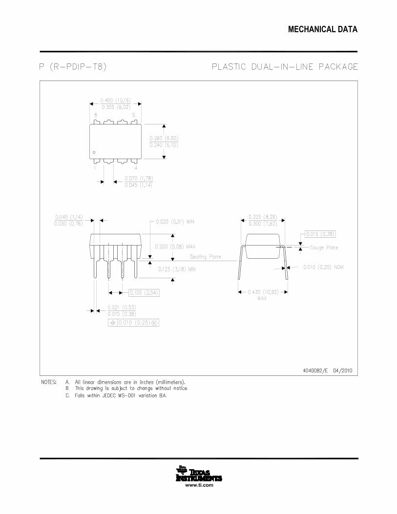
12 Mechanical, Packaging, and Orderable7.2 Functional Block Diagram ......................................... 9Information ........................................................... 257.3 Feature Description................................................... 9
4 Revision HistoryNOTE: Page numbers for previous revisions may differ from page numbers in the current version.
Changes from Revision F (November 2004) to Revision G Page
• Added ESD Ratings table, Feature Description section, Device Functional Modes, Application and Implementationsection, Power Supply Recommendations section, Layout section, Device and Documentation Support section, andMechanical, Packaging, and Orderable Information section. ................................................................................................ 1
2 Submit Documentation Feedback Copyright © 1990–2015, Texas Instruments Incorporated
Product Folder Links: LT1054
1
2
3
4
5
6
7
8
16
15
14
13
12
11
10
9
NC
NC
FB/SD
CAP+
GND
CAP−
NC
NC
NC
NC
VCC
OSC
VREF
VOUT
NC
NC
NC − No internal connection
1
2
3
4
8
7
6
5
FB/SD
CAP+
GND
CAP−
VCC
OSC
VREF
VOUT
LT1054www.ti.com SLVS033G –FEBRUARY 1990–REVISED JULY 2015
5 Pin Configuration and Functions
P Package8-Pin PDIPTop View
DW Package16-Pin SOIC
Top View
Pin FunctionsPIN
I/O DESCRIPTIONNAME PDIP SOICFB/SD 1 3 Input Shutdown for low Iq operation or error amp input for regulationCAP+ 2 4 Input Positive side of CINGND 3 5 — GroundCAP- 4 6 Input Negative side of CINVOUT 5 11 Output Regulated output voltageVREF 6 12 Output Internal Reference VoltageOSC 7 13 Input Oscillator control pinVCC 8 14 — Supply pin
1, 2, 7, 8, 9,NC — — No connect (no internal connection)10, 15, 16
Copyright © 1990–2015, Texas Instruments Incorporated Submit Documentation Feedback 3
Product Folder Links: LT1054
LT1054SLVS033G –FEBRUARY 1990–REVISED JULY 2015 www.ti.com
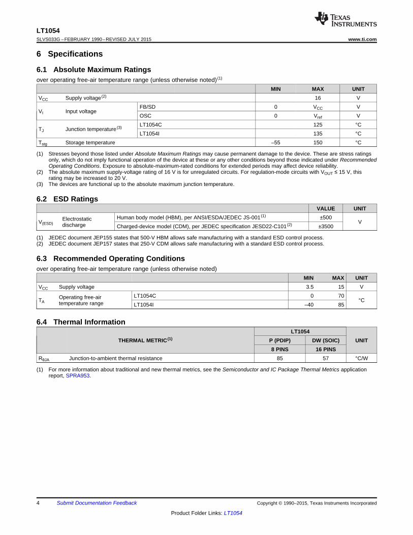
6 Specifications
6.1 Absolute Maximum Ratingsover operating free-air temperature range (unless otherwise noted) (1)
MIN MAX UNITVCC Supply voltage (2) 16 V
FB/SD 0 VCC VVI Input voltage
OSC 0 Vref VLT1054C 125 °C
TJ Junction temperature (3)LT1054I 135 °C
Tstg Storage temperature –55 150 °C
(1) Stresses beyond those listed under Absolute Maximum Ratings may cause permanent damage to the device. These are stress ratingsonly, which do not imply functional operation of the device at these or any other conditions beyond those indicated under RecommendedOperating Conditions. Exposure to absolute-maximum-rated conditions for extended periods may affect device reliability.
(2) The absolute maximum supply-voltage rating of 16 V is for unregulated circuits. For regulation-mode circuits with VOUT ≤ 15 V, thisrating may be increased to 20 V.
(3) The devices are functional up to the absolute maximum junction temperature.
6.2 ESD RatingsVALUE UNIT
Human body model (HBM), per ANSI/ESDA/JEDEC JS-001 (1) ±500ElectrostaticV(ESD) Vdischarge Charged-device model (CDM), per JEDEC specification JESD22-C101 (2) ±3500
(1) JEDEC document JEP155 states that 500-V HBM allows safe manufacturing with a standard ESD control process.(2) JEDEC document JEP157 states that 250-V CDM allows safe manufacturing with a standard ESD control process.
6.3 Recommended Operating Conditionsover operating free-air temperature range (unless otherwise noted)
MIN MAX UNITVCC Supply voltage 3.5 15 V
LT1054C 0 70Operating free-airTA °Ctemperature range LT1054I –40 85
6.4 Thermal InformationLT1054
THERMAL METRIC (1) P (PDIP) DW (SOIC) UNIT8 PINS 16 PINS
RθJA Junction-to-ambient thermal resistance 85 57 °C/W
(1) For more information about traditional and new thermal metrics, see the Semiconductor and IC Package Thermal Metrics applicationreport, SPRA953.
4 Submit Documentation Feedback Copyright © 1990–2015, Texas Instruments Incorporated
Product Folder Links: LT1054
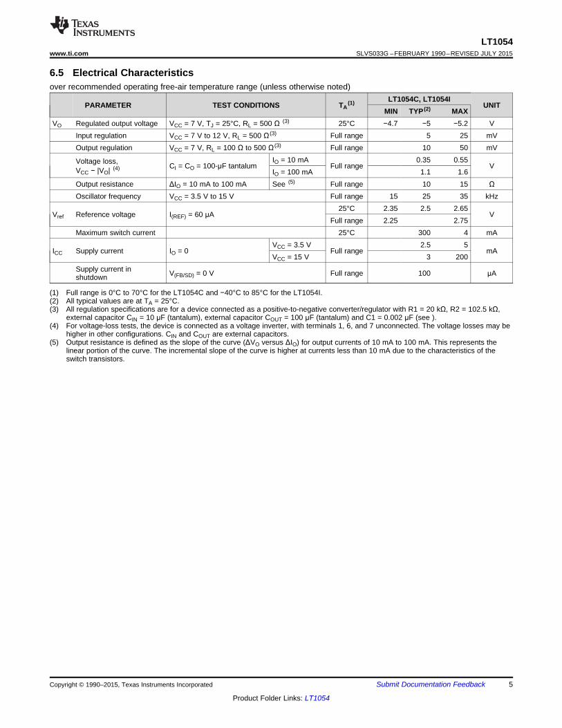
LT1054www.ti.com SLVS033G –FEBRUARY 1990–REVISED JULY 2015
6.5 Electrical Characteristicsover recommended operating free-air temperature range (unless otherwise noted)
LT1054C, LT1054IPARAMETER TEST CONDITIONS TA
(1) UNITMIN TYP (2) MAX
VO Regulated output voltage VCC = 7 V, TJ = 25°C, RL = 500 Ω (3) 25°C −4.7 −5 −5.2 VInput regulation VCC = 7 V to 12 V, RL = 500 Ω (3) Full range 5 25 mVOutput regulation VCC = 7 V, RL = 100 Ω to 500 Ω (3) Full range 10 50 mV
IO = 10 mA 0.35 0.55Voltage loss, CI = CO = 100-μF tantalum Full range VVCC − |VO| (4) IO = 100 mA 1.1 1.6Output resistance ΔIO = 10 mA to 100 mA See (5) Full range 10 15 ΩOscillator frequency VCC = 3.5 V to 15 V Full range 15 25 35 kHz
25°C 2.35 2.5 2.65Vref Reference voltage I(REF) = 60 μA V
Full range 2.25 2.75Maximum switch current 25°C 300 4 mA
VCC = 3.5 V 2.5 5ICC Supply current IO = 0 Full range mA
VCC = 15 V 3 200Supply current in V(FB/SD) = 0 V Full range 100 μAshutdown
(1) Full range is 0°C to 70°C for the LT1054C and −40°C to 85°C for the LT1054I.(2) All typical values are at TA = 25°C.(3) All regulation specifications are for a device connected as a positive-to-negative converter/regulator with R1 = 20 kΩ, R2 = 102.5 kΩ,
external capacitor CIN = 10 μF (tantalum), external capacitor COUT = 100 μF (tantalum) and C1 = 0.002 μF (see ).(4) For voltage-loss tests, the device is connected as a voltage inverter, with terminals 1, 6, and 7 unconnected. The voltage losses may be
higher in other configurations. CIN and COUT are external capacitors.(5) Output resistance is defined as the slope of the curve (ΔVO versus ΔIO) for output currents of 10 mA to 100 mA. This represents the
linear portion of the curve. The incremental slope of the curve is higher at currents less than 10 mA due to the characteristics of theswitch transistors.
Copyright © 1990–2015, Texas Instruments Incorporated Submit Documentation Feedback 5
Product Folder Links: LT1054
2
1
00 5 10 15
−S
up
ply
Cu
rren
t−
mA
3
4
5
CC
I
IO = 0
VCC − Input Voltage − V
0.3
0.2
0.1
0−50 −25 0 25 50 75 100
Sh
utd
ow
nT
hre
sh
old
Vo
ltag
e−
V
0.4
0.5
0.6
TA − Free-Air Temperature − °C
V(FB/SD)
LT1054SLVS033G –FEBRUARY 1990–REVISED JULY 2015 www.ti.com
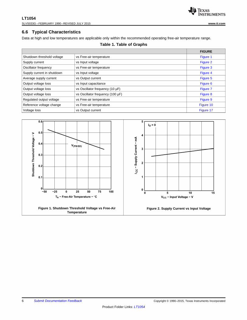
6.6 Typical CharacteristicsData at high and low temperatures are applicable only within the recommended operating free-air temperature range.
Table 1. Table of GraphsFIGURE
Shutdown threshold voltage vs Free-air temperature Figure 1Supply current vs Input voltage Figure 2Oscillator frequency vs Free-air temperature Figure 3Supply current in shutdown vs Input voltage Figure 4Average supply current vs Output current Figure 5Output voltage loss vs Input capacitance Figure 6Output voltage loss vs Oscillator frequency (10 µF) Figure 7Output voltage loss vs Oscillator frequency (100 µF) Figure 8Regulated output voltage vs Free-air temperature Figure 9Reference voltage change vs Free-air temperature Figure 10Voltage loss vs Output current Figure 17
Figure 1. Shutdown Threshold Voltage vs Free-Air Figure 2. Supply Current vs Input VoltageTemperature
6 Submit Documentation Feedback Copyright © 1990–2015, Texas Instruments Incorporated
Product Folder Links: LT1054
0
1 10 100
Ou
tpu
tV
olt
ag
eL
oss
−V
2
1
IO = 100 mA
IO = 50 mA
IO = 10 mA
Inverter Configuration
CIN = 10-μF Tantalum
COUT = 100-μF Tantalum
Oscillator Frequency − kHz
0.75
0.5
0.25
1.25
1.5
1.75
2.25
2.5
0
1 10 100
Ou
tpu
tV
olt
ag
eL
oss
−V
2
1
IO = 100 mA
IO = 50 mA
IO = 10 mA
Inverter Configuration
CIN = 100-μF Tantalum
COUT = 100-μF Tantalum
Oscillator Frequency − kHz
0.25
0.5
0.75
1.25
1.5
1.75
2.25
2.5
0.4
0.2
1.2
00 10 20 30 40 50 60
Ou
tpu
tV
olt
ag
eL
oss
−V
0.8
0.6
1.0
1.4
70 80 90 100
IO = 100 mA
IO = 50 mA
IO = 10 mA
Inverter Configuration
COUT = 100-μF Tantalum
fOSC = 25 kHz
Input Capacitance − μF
40
20
120
00 20 40 60
Avera
ge
Su
pp
ly C
urr
en
t−
mA
80
60
100
140
80 100
IO − Output Current − mA
25
15−50 −25 0 25 50 75
Oscilla
tor
Fre
qu
en
cy
−kH
z
35
100
21
VCC = 15 V
VCC = 3.5 V
TA − Free-Air Temperature − °C
19
17
23
27
29
31
33
60
40
20
00 5
Su
pp
ly C
urr
en
t in
Sh
utd
ow
n−
80
100
120
10 15
μA
VCC − Input Voltage − V
V(FB/SD) = 0
LT1054www.ti.com SLVS033G –FEBRUARY 1990–REVISED JULY 2015
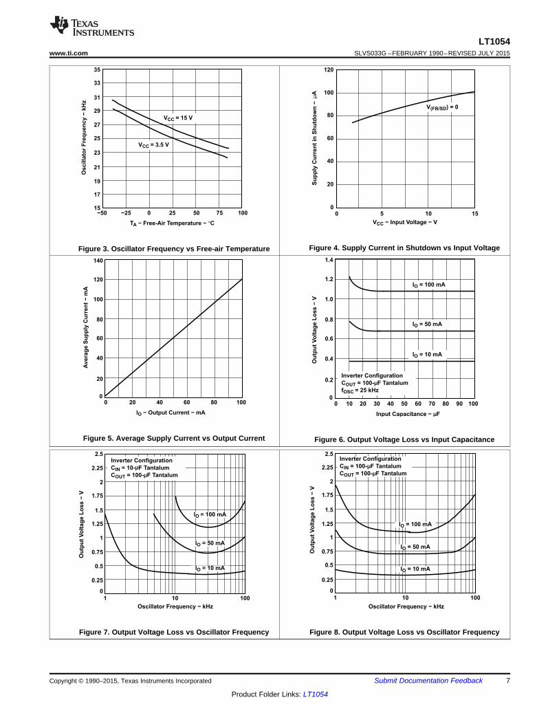
Figure 4. Supply Current in Shutdown vs Input VoltageFigure 3. Oscillator Frequency vs Free-air Temperature
Figure 5. Average Supply Current vs Output Current Figure 6. Output Voltage Loss vs Input Capacitance
Figure 7. Output Voltage Loss vs Oscillator Frequency Figure 8. Output Voltage Loss vs Oscillator Frequency
Copyright © 1990–2015, Texas Instruments Incorporated Submit Documentation Feedback 7
Product Folder Links: LT1054
−12
−12.4
−4.9
−12.6−50 −25 0 25 50
−R
eg
ula
ted
Ou
tpu
tV
olt
ag
e−
V
−5.1
−11.8
−5
−4.7
75 100
−4.8
−11.6
−12.2VO
TA − Free-Air Temperature − °C
−40
−80
60
−100−50 −25 0 25 50
−R
efe
ren
ce
Vo
ltag
e C
han
ge
−m
V
20
−20
40
100
75 100 125
80
0
−60
TA − Free-Air Temperature − °C
∆V
ref
VREF at 0 = 2.500 V
LT1054SLVS033G –FEBRUARY 1990–REVISED JULY 2015 www.ti.com
Figure 9. Regulated Output Voltage vs Free-air Temperature Figure 10. Reference Voltage Change vs Free-airTemperature
8 Submit Documentation Feedback Copyright © 1990–2015, Texas Instruments Incorporated
Product Folder Links: LT1054
VREF
Ref
+
−
OSCQ
Q
Drive
CAP +
VCC
GND
VOUT
FB/SD
OSC
2.5 V
CAP −
COUT†
CIN†
† External capacitors
Drive
Drive
Drive
R
R
1
7
3
5
2
4
86
LT1054www.ti.com SLVS033G –FEBRUARY 1990–REVISED JULY 2015
7 Detailed Description
7.1 OverviewLT1054 is a "negative voltage generator" or "negative charge pump" that will output a negative voltage that isproportional to the input voltage (or VCC). With proper supply voltage, VOUT will regulate to an unregulated VOUTthat is approximately –VCC (reduced by a small voltage loss). If a lower absolute voltage is desired, VOUT can beregulated to that value when proper feedback resistors are applied.
LT1054 regulates up to 100mA with minimal loss and has a shutdown mode that makes this part optimal acrossa wide range of applications.
7.2 Functional Block Diagram
Pin numbers shown are for the P package.
7.3 Feature Description
7.3.1 Reference and Error Amplifier for RegulationThe feedback/shutdown (FB/SD) terminal has two functions. Pulling FB/SD below the shutdown threshold (≈ 0.45V) puts the device into shutdown. In shutdown, the reference/regulator is turned off and switching stops. Theswitches are set such that both CIN and COUT are discharged through the output load. Quiescent current inshutdown drops to approximately 100 µA. Any open-collector gate can be used to put the LT1054 into shutdown.For normal (unregulated) operation, the device will restart when the external gate is shut off. In LT1054 circuitsthat use the regulation feature, the external resistor divider can provide enough pulldown to keep the device inshutdown until the output capacitor (COUT) has fully discharged. For most applications, where the LT1054 is runintermittently, this does not present a problem because the discharge time of the output capacitor is shortcompared to the off time of the device. In applications where the device has to start up before the outputcapacitor (COUT) has fully discharged, a restart pulse must be applied to FB/SD of the LT1054. Using the circuitshown in Figure 11, the restart signal can be either a pulse (tp > 100 µs) or a logic high. Diode coupling therestart signal into FB/SD allows the output voltage to rise and regulate without overshoot. The resistor dividerR3/R4 shown in Figure 11 should be chosen to provide a signal level at FB/SD of 0.7−1.1 V.
FB/SD also is the inverting input of the LT1054 error amplifier and, as such, can be used to obtain a regulatedoutput voltage.
Copyright © 1990–2015, Texas Instruments Incorporated Submit Documentation Feedback 9
Product Folder Links: LT1054
C1
LT1054
VOUT
VREF
OSC
VCC
CAP−
GND
CAP+
FB/SD
C2
VIN
+
1
2
3
4
8
7
6
5
VIN
R2
R1R4
R3
Restart Shutdown
C1
5
6
7
8
+CIN
10- Fμ
Tantalum
4
3
2
1
LT1054
VOUT
VREF
OSC
VCC
CAP−
GND
CAP+
FB/SD
VOUT
Where: R1 = 20 kΩ
VREF = 2.5 V Nominal
+2.2μF
For example: To get VO = −5 V, referenced to the ground terminal of the LT1054
COUT
100- Fμ
Tantalum
OUT
REF
V 5 VR2 R1 1 20 k 1 102.6 k †
V 2.5 V40 mV40 mV
22
æ ö æ öç ÷ ç ÷-
= + = W + = Wç ÷ ç ÷ç ÷ ç ÷-- ç ÷ç ÷
è øè ø
† Choose the closest 1% value.
LT1054SLVS033G –FEBRUARY 1990–REVISED JULY 2015 www.ti.com
Feature Description (continued)
Figure 11. Basic Regulation Configuration
7.3.2 External Oscillator SynchronizationThis pin can be used to raise or lower the oscillator frequency or to synchronize the device to an external clock.Internally Pin 7 is connected to the oscillator timing capacitor (Ct ≈ 150pF) which is alternately charged anddischarged by current sources of ±7µA so that the duty cycle is ≈50%. The LT1054 oscillator is designed to runin the frequency band where switching losses are minimized. However the frequency can be raised, lowered, orsynchronized to an external system clock if necessary.
Figure 12. External-Clock System
The frequency can be lowered by adding an external capacitor (C1, Figure 12) from Pin 7 to ground. This willincrease the charge and discharge times which lowers the oscillator frequency. The frequency can be increasedby adding an external capacitor (C2, Figure 12, in the range of 5pF to 20pF) from Pin 2 to Pin 7. This capacitorwill couple charge into CT at the switch transitions, which will shorten the charge and discharge time, raising theoscillator frequency. Synchronization can be accomplished by adding an external resistive pull-up from Pin 7 to
10 Submit Documentation Feedback Copyright © 1990–2015, Texas Instruments Incorporated
Product Folder Links: LT1054
C2C1
V2
f
V1
RL
EQUIV
V1 V2 V1 V2I
(1/ fC1) R
- -
= =
LT1054www.ti.com SLVS033G –FEBRUARY 1990–REVISED JULY 2015
Feature Description (continued)the reference pin (Pin 6). A 20k pull-up is recommended. An open collector gate or an NPN transistor can thenbe used to drive the oscillator pin at the external clock frequency as shown in Figure 12. Pulling up Pin 7 to anexternal voltage is not recommended. For circuits that require both frequency synchronization and regulation, anexternal reference can be used as the reference point for the top of the R1/R2 divider allowing Pin 6 to be usedas a pullup point for Pin 7.
7.3.3 Output Current and Voltage LossThe functional block diagram shows that the maximum regulated output voltage is limited by the supply voltage.For the basic configuration, |VOUT| referenced to the ground terminal of the LT1054 must be less than the total ofthe supply voltage minus the voltage loss due to the switches. The voltage loss versus output current due to theswitches can be found in the typical performance curves. Other configurations, such as the negative doubler, canprovide higher voltages at reduced output currents.
7.3.4 Reference VoltageReference Output. This pin provides a 2.5V reference point for use in LT1054-based regulator circuits. Thetemperature coefficient of the reference voltage has been adjusted so that the temperature coefficient of theregulated output voltage is close to zero. This requires the reference output to have a positive temperaturecoefficient as can be seen in the typical performance curves. This nonzero drift is necessary to offset a drift terminherent in the internal reference divider and comparator network tied to the feedback pin. The overall result ofthese drift terms is a regulated output which has a slight positive temperature coefficient at output voltages below5V and a slight negative TC at output voltages above 5V. Reference output current should be limited, forregulator feedback networks, to approximately 60µA. The reference pin will draw ≈100µA when shorted toground and will not affect the internal reference/regulator, so that this pin can also be used as a pull-up forLT1054 circuits that require synchronization.
7.4 Device Functional Modes
7.4.1 Main OperationA review of a basic switched-capacitor building block is helpful in understanding the operation of the LT1054.When the switch shown in Figure 13 is in the left position, capacitor C1 charges to the voltage at V1. The totalcharge on C1 is q1 = C1*V1. When the switch is moved to the right, C1 is discharged to the voltage at V2. Afterthis discharge time, the charge on C1 is q2 = C1*V2. The charge has been transferred from the source V1 to theoutput V2. The amount of charge transferred is shown in Equation 1.
Δq = q1 – q2 = C1(V1 – V2) (1)
If the switch is cycled f times per second, the charge transfer per unit time (that is, current) is as shown inEquation 2.I = f × L\q = f × C1(1 – V2) (2)
To obtain an equivalent resistance for a switched-capacitor network, this equation can be rewritten in terms ofvoltage and impedance equivalence as shown in Equation 3.
(3)
Figure 13. Switched-Capacitor Building Block
Copyright © 1990–2015, Texas Instruments Incorporated Submit Documentation Feedback 11
Product Folder Links: LT1054
C2
V2V1
R
R
L
EQUIV
REQUIV
1
fC1
LT1054SLVS033G –FEBRUARY 1990–REVISED JULY 2015 www.ti.com
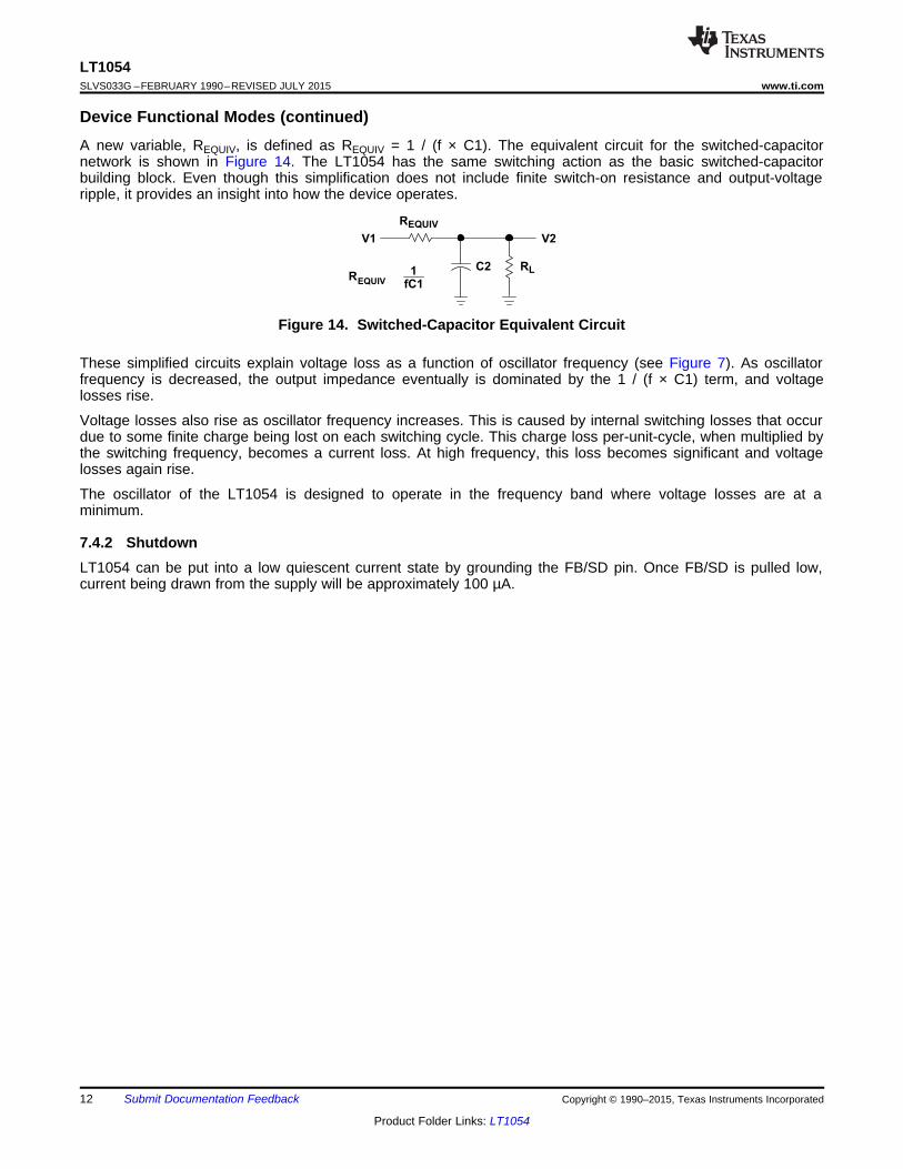
Device Functional Modes (continued)A new variable, REQUIV, is defined as REQUIV = 1 / (f × C1). The equivalent circuit for the switched-capacitornetwork is shown in Figure 14. The LT1054 has the same switching action as the basic switched-capacitorbuilding block. Even though this simplification does not include finite switch-on resistance and output-voltageripple, it provides an insight into how the device operates.
Figure 14. Switched-Capacitor Equivalent Circuit
These simplified circuits explain voltage loss as a function of oscillator frequency (see Figure 7). As oscillatorfrequency is decreased, the output impedance eventually is dominated by the 1 / (f × C1) term, and voltagelosses rise.
Voltage losses also rise as oscillator frequency increases. This is caused by internal switching losses that occurdue to some finite charge being lost on each switching cycle. This charge loss per-unit-cycle, when multiplied bythe switching frequency, becomes a current loss. At high frequency, this loss becomes significant and voltagelosses again rise.
The oscillator of the LT1054 is designed to operate in the frequency band where voltage losses are at aminimum.
7.4.2 ShutdownLT1054 can be put into a low quiescent current state by grounding the FB/SD pin. Once FB/SD is pulled low,current being drawn from the supply will be approximately 100 µA.
12 Submit Documentation Feedback Copyright © 1990–2015, Texas Instruments Incorporated
Product Folder Links: LT1054
R2
R1
20 kΩLT1054
VOUT
VREF
OSC
VCC
CAP−
GND
CAP+
FB/SD
VOUT
100 μF
0.002 μF
10 μF
2
3
4
8
7
6
5
+
+ +
VIN
+2 μF
OUT OUT
REF
V VR2 R1 1 20 k 1
V 1.21 V40 mV
2
æ öç ÷ æ ö
= + = W +ç ÷ ç ÷ç ÷ç ÷ è ø-ç ÷è ø
LT1054www.ti.com SLVS033G –FEBRUARY 1990–REVISED JULY 2015
8 Application and Implementation
NOTEInformation in the following applications sections is not part of the TI componentspecification, and TI does not warrant its accuracy or completeness. TI’s customers areresponsible for determining suitability of components for their purposes. Customers shouldvalidate and test their design implementation to confirm system functionality.
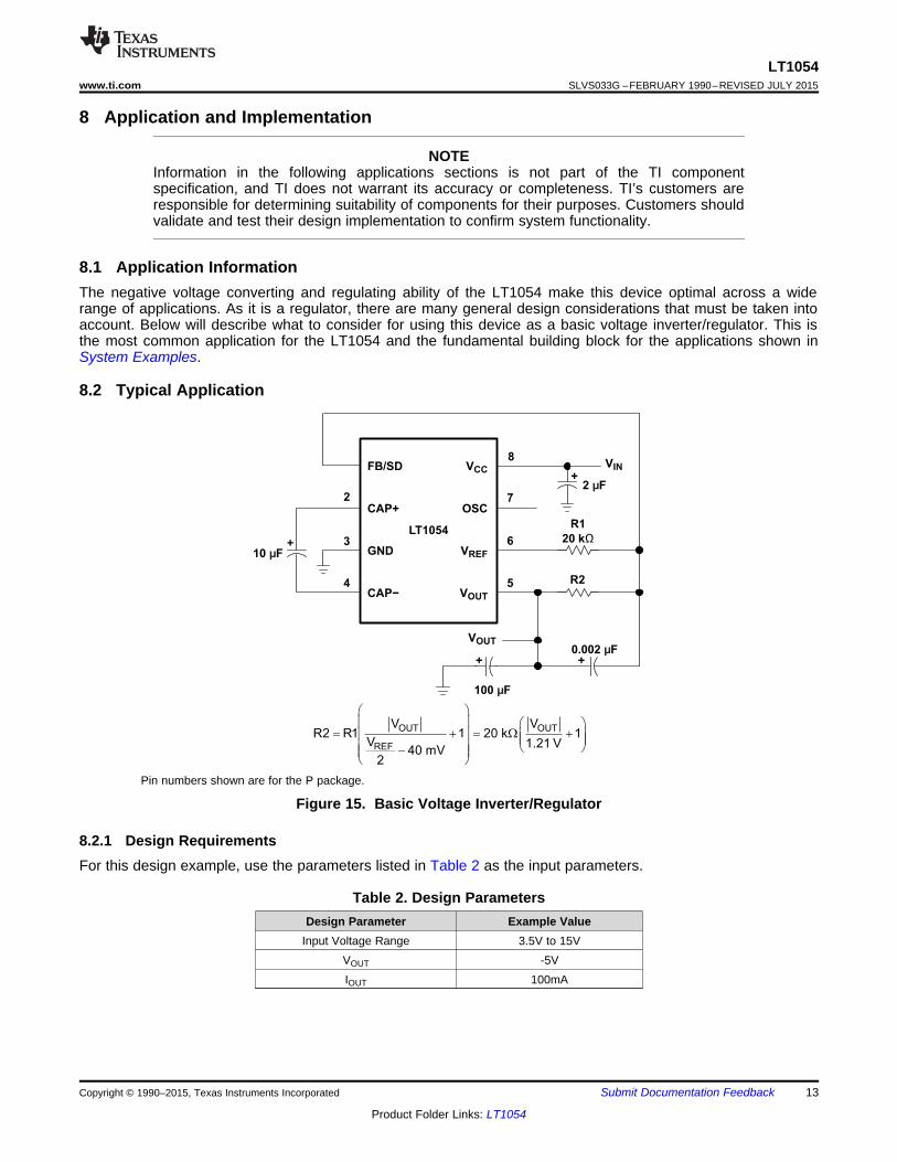
8.1 Application InformationThe negative voltage converting and regulating ability of the LT1054 make this device optimal across a widerange of applications. As it is a regulator, there are many general design considerations that must be taken intoaccount. Below will describe what to consider for using this device as a basic voltage inverter/regulator. This isthe most common application for the LT1054 and the fundamental building block for the applications shown inSystem Examples.
8.2 Typical Application
Pin numbers shown are for the P package.
Figure 15. Basic Voltage Inverter/Regulator
8.2.1 Design RequirementsFor this design example, use the parameters listed in Table 2 as the input parameters.
Table 2. Design ParametersDesign Parameter Example Value
Input Voltage Range 3.5V to 15VVOUT -5VIOUT 100mA
Copyright © 1990–2015, Texas Instruments Incorporated Submit Documentation Feedback 13
Product Folder Links: LT1054
OUT
OUT
IV
2fCD =
LT1054SLVS033G –FEBRUARY 1990–REVISED JULY 2015 www.ti.com
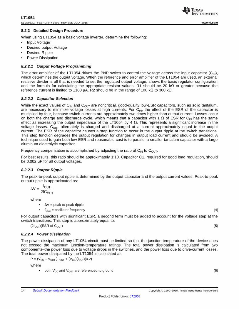
8.2.2 Detailed Design ProcedureWhen using LT1054 as a basic voltage inverter, determine the following:• Input Voltage• Desired output Voltage• Desired Ripple• Power Dissipation
8.2.2.1 Output Voltage ProgrammingThe error amplifier of the LT1054 drives the PNP switch to control the voltage across the input capacitor (CIN),which determines the output voltage. When the reference and error amplifier of the LT1054 are used, an externalresistive divider is all that is needed to set the regulated output voltage. shows the basic regulator configurationand the formula for calculating the appropriate resistor values. R1 should be 20 kΩ or greater because thereference current is limited to ±100 μA. R2 should be in the range of 100 kΩ to 300 kΩ.
8.2.2.2 Capacitor SelectionWhile the exact values of CIN and COUT are noncritical, good-quality low-ESR capacitors, such as solid tantalum,are necessary to minimize voltage losses at high currents. For CIN, the effect of the ESR of the capacitor ismultiplied by four, because switch currents are approximately two times higher than output current. Losses occuron both the charge and discharge cycle, which means that a capacitor with 1 Ω of ESR for CIN has the sameeffect as increasing the output impedance of the LT1054 by 4 Ω. This represents a significant increase in thevoltage losses. COUT alternately is charged and discharged at a current approximately equal to the outputcurrent. The ESR of the capacitor causes a step function to occur in the output ripple at the switch transitions.This step function degrades the output regulation for changes in output load current and should be avoided. Atechnique used to gain both low ESR and reasonable cost is to parallel a smaller tantalum capacitor with a largealuminum electrolytic capacitor.
Frequency compensation is accomplished by adjusting the ratio of CIN to COUT.
For best results, this ratio should be approximately 1:10. Capacitor C1, required for good load regulation, shouldbe 0.002 μF for all output voltages.
8.2.2.3 Output RippleThe peak-to-peak output ripple is determined by the output capacitor and the output current values. Peak-to-peakoutput ripple is approximated as:
where• ΔV = peak-to-peak ripple• fOSC = oscillator frequency (4)
For output capacitors with significant ESR, a second term must be added to account for the voltage step at theswitch transitions. This step is approximately equal to:
(2IOUT)(ESR of COUT) (5)
8.2.2.4 Power DissipationThe power dissipation of any LT1054 circuit must be limited so that the junction temperature of the device doesnot exceed the maximum junction-temperature ratings. The total power dissipation is calculated from twocomponents–the power loss due to voltage drops in the switches, and the power loss due to drive-current losses.The total power dissipated by the LT1054 is calculated as:
P = (VCC – VOUT ) IOUT + (VCC)(IOUT)(0.2)
where• both VCC and VOUT are referenced to ground (6)
14 Submit Documentation Feedback Copyright © 1990–2015, Texas Instruments Incorporated
Product Folder Links: LT1054
x
4.9 VR 11
(4.4)(100 mA)= = W
VIN
COUT
R2
R1
C1
LT1054
VOUT
VREF
OSC
VCC
CAP−
GND
CAP+
FB/SD
VOUT
Rx
CIN
+
+
1
2
3
4
8
7
6
5
P (12 V | 5 V |)(100 mA) (12 V)(100 mA)(0.2)
P 700 mW 240 mW 940 mW
= - - +
= + =
xx
OUT
VR
4.4 I=
LT1054www.ti.com SLVS033G –FEBRUARY 1990–REVISED JULY 2015
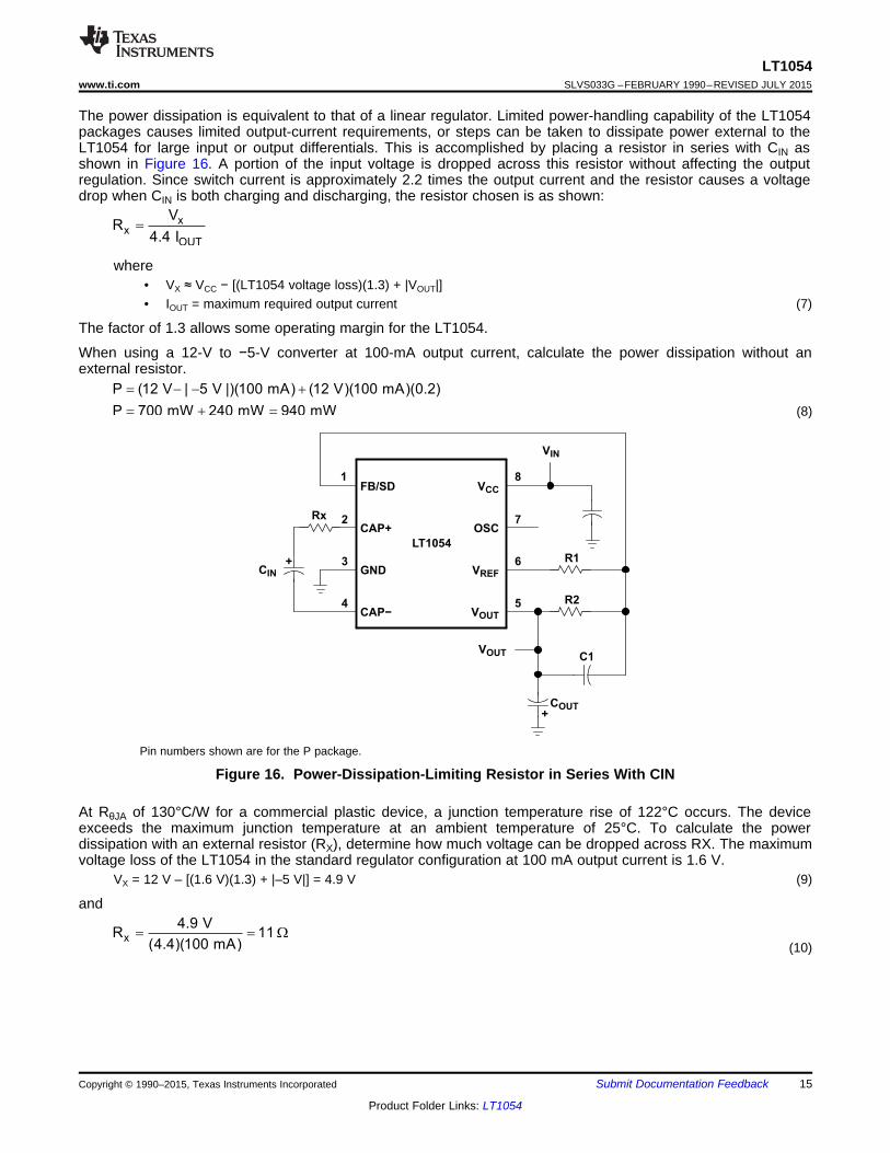
The power dissipation is equivalent to that of a linear regulator. Limited power-handling capability of the LT1054packages causes limited output-current requirements, or steps can be taken to dissipate power external to theLT1054 for large input or output differentials. This is accomplished by placing a resistor in series with CIN asshown in Figure 16. A portion of the input voltage is dropped across this resistor without affecting the outputregulation. Since switch current is approximately 2.2 times the output current and the resistor causes a voltagedrop when CIN is both charging and discharging, the resistor chosen is as shown:
where• VX ≈ VCC − [(LT1054 voltage loss)(1.3) + |VOUT|]• IOUT = maximum required output current (7)
The factor of 1.3 allows some operating margin for the LT1054.
When using a 12-V to −5-V converter at 100-mA output current, calculate the power dissipation without anexternal resistor.
(8)
Pin numbers shown are for the P package.
Figure 16. Power-Dissipation-Limiting Resistor in Series With CIN
At RθJA of 130°C/W for a commercial plastic device, a junction temperature rise of 122°C occurs. The deviceexceeds the maximum junction temperature at an ambient temperature of 25°C. To calculate the powerdissipation with an external resistor (RX), determine how much voltage can be dropped across RX. The maximumvoltage loss of the LT1054 in the standard regulator configuration at 100 mA output current is 1.6 V.
VX = 12 V – [(1.6 V)(1.3) + |–5 V|] = 4.9 V (9)
and
(10)
Copyright © 1990–2015, Texas Instruments Incorporated Submit Documentation Feedback 15
Product Folder Links: LT1054
10 V
1N5817
MotorTach
1N4002
LT1054
VOUT
VREF
OSC
VCC
CAP−
GND
CAP+
FB/SD100-kΩ
Speed Control5 μF
100 kΩ
10 μF+
+
1
2
3
4
8
7
6
5
+
−+
−
1
00 10 20 30 40 50 60
Vo
ltag
e L
oss
−V
Output Current − mA
2
70 80 90 100
TJ = 125°C
TJ = 25°C
3.5 V ≤ VCC ≤ 15 V
Ci = Co = 100 μF
TJ = −55°C
0.8
0.6
0.4
0.2
1.2
1.4
1.6
1.8
LT1054SLVS033G –FEBRUARY 1990–REVISED JULY 2015 www.ti.com
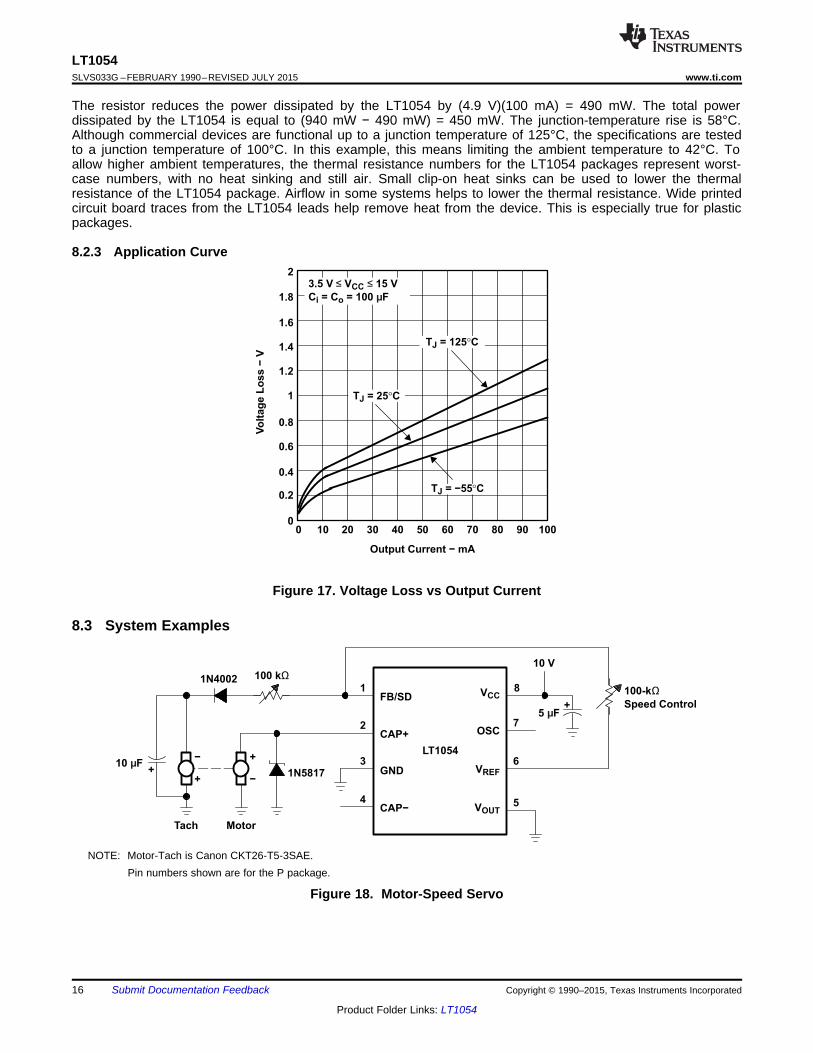
The resistor reduces the power dissipated by the LT1054 by (4.9 V)(100 mA) = 490 mW. The total powerdissipated by the LT1054 is equal to (940 mW − 490 mW) = 450 mW. The junction-temperature rise is 58°C.Although commercial devices are functional up to a junction temperature of 125°C, the specifications are testedto a junction temperature of 100°C. In this example, this means limiting the ambient temperature to 42°C. Toallow higher ambient temperatures, the thermal resistance numbers for the LT1054 packages represent worst-case numbers, with no heat sinking and still air. Small clip-on heat sinks can be used to lower the thermalresistance of the LT1054 package. Airflow in some systems helps to lower the thermal resistance. Wide printedcircuit board traces from the LT1054 leads help remove heat from the device. This is especially true for plasticpackages.
8.2.3 Application Curve
Figure 17. Voltage Loss vs Output Current
8.3 System Examples
NOTE: Motor-Tach is Canon CKT26-T5-3SAE.Pin numbers shown are for the P package.
Figure 18. Motor-Speed Servo
16 Submit Documentation Feedback Copyright © 1990–2015, Texas Instruments Incorporated
Product Folder Links: LT1054
VIN
3.5 V to 15 V
1N40011N4001
VOUT
LT1054
VOUT
VREF
OSC
VCC
CAP−
GND
CAP+
FB/SD
2 μF
10 μF100 μF
VIN = 3.5 V to 15 V
VOUT ≈ 2 VIN − (VL + 2 V Diode)
VL = LT1054 Voltage Loss
+
+
−
+
1
2
3
4
8
7
6
5
+
LT1054
VOUT
VREF
OSC
VCC
CAP−
GND
CAP+
FB/SD
R
V
X
IN
VOUT
10 Fμ
100 μF
QV
X
IN
VIN = −3.5 V to −15 V
VOUT = 2 VIN + (LT1054 Voltage Loss) + (QX Saturation Voltage)
2 μF
1
2
3
4
8
7
6
5
+
−
+
+
+
LT1054www.ti.com SLVS033G –FEBRUARY 1990–REVISED JULY 2015
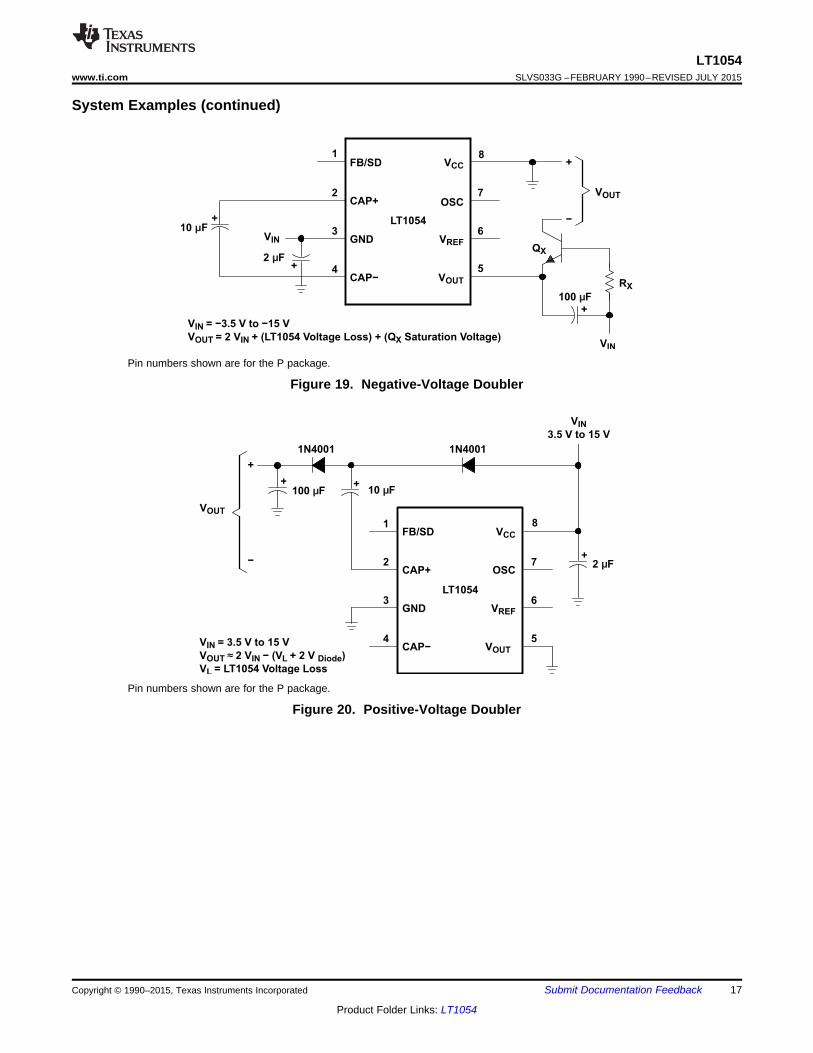
System Examples (continued)
Pin numbers shown are for the P package.
Figure 19. Negative-Voltage Doubler
Pin numbers shown are for the P package.
Figure 20. Positive-Voltage Doubler
Copyright © 1990–2015, Texas Instruments Incorporated Submit Documentation Feedback 17
Product Folder Links: LT1054
VREF
+VO
LT1054
VOUT
OSC
VCC
CAP−
GND
CAP+
FB/SD
10 Fμ
10 μF
100 μF
10 μF
100 μF
−VO100 μF
VI
3.5 V to 15 V
VI = 3.5 V to 15 V
+VO ≈ 2 VIN − (VL + 2 VDiode) −VO ≈ −2 VI + (VL + 2 VDiode)
VL = LT1054 Voltage Loss
1N4001
1N4001
1N4001
1N40011N4001
+
+
+
1
2
3
4
8
7
6
5 +
+
−
+
+
−
+
R2
500 kΩ
VIN
3.5 V to 15 V
CAP+ of
LT1054 #1
HP5082-2810
1N4002
1N4002
1N4002
VOUT
SET
R1
40 kΩ
1N4002
LT1054 #1
VOUT
VREF
OSC
VCC
CAP−
GND
CAP+
FB/SD
VOUT
VREF
OSC
VCC
CAP−
GND
CAP+
FB/SD
VOUT
IOUT ≅100 mA MAX
10 μF
2.2 μF
20 kΩ
0.002 μF10 μF
100 μF
10 μF
10 μF
10 μF
10 μF
1N4002
VIN = 3.5 V to 15 V
VOUT MAX ≈ −2 VIN + [LT1054 Voltage Loss +2 (VDiode)]
LT1054 #2
1
2
3
4
8
7
6
5
+
1
2
3
4
8
7
6
5
+
+
+
+
+
+
+
+
OUT OUT
REF
V VR2 R1 1 R1 1
V 1.21 V40 m V
2
æ öç ÷ æ ö
= + = +ç ÷ ç ÷ç ÷ç ÷ è ø-ç ÷è ø
LT1054SLVS033G –FEBRUARY 1990–REVISED JULY 2015 www.ti.com
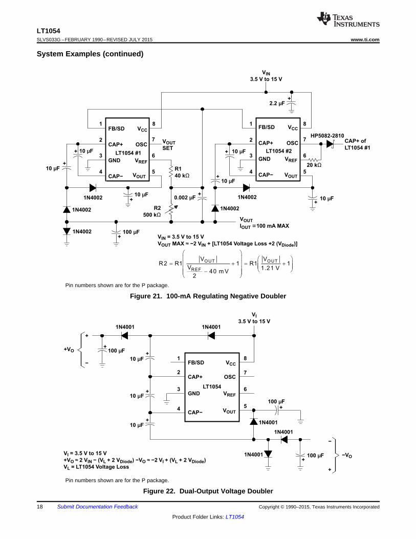
System Examples (continued)
Pin numbers shown are for the P package.
Figure 21. 100-mA Regulating Negative Doubler
Pin numbers shown are for the P package.
Figure 22. Dual-Output Voltage Doubler
18 Submit Documentation Feedback Copyright © 1990–2015, Texas Instruments Incorporated
Product Folder Links: LT1054
10 kΩ
2N2222
5 V
A1
A2
Gain Trim
5 kΩ
5 V
2N2907
LT1054 #1
CAP−
GND
FB/SD
200 kΩ
VOUT
VREF
VCC
CAP+ OSC
10 μF
100- Fμ
Tantalum
3 kΩ
0.022 μF
10 kΩ 10 μF
1 μF
5 kΩ
10 kΩ
301 kΩ
40 Ω
350 Ω
100 kΩ
100 kΩ
1 MΩ
1/2
LT1013
Input TTL or
CMOS Low
for On Zero Trim
10 kΩ
Adjust Gain Trim For 3 V Out From
Full-Scale Bridge Output of 24 mV
VOUT
1
2
3
4
8
7
6
5
+
+
−2
3
8
1
+
−1/2
LT1013
+
6
5
7
4
+
VCC
OSC
VREF
VOUT
HP5082-2810
VO = −5 V
IO = 0-200 mA
R2
200 kΩ
R1
39.2 kΩ
12 V
FB/SD
CAP+
GND
CAP−
LT1054 #2
VCC
OSC
VREF
VOUT
LT1054 #1
CAP−
GND
CAP+
FB/SD
5 μF
10 Ω
1/2 W
10 μF
0.002 μF
10 μF
20 kΩ
200 μF
10 Ω
1/2 W
+
1
2
4
8
7
6
5
3
1
2
4
8
7
6
5
3
+
+
+
+
OUT OUT
REF
V VR2 R1 1 R1 1
V 1.21 V40 mV
2
æ öç ÷ æ ö
= + = +ç ÷ ç ÷ç ÷ç ÷ è ø-ç ÷è ø
LT1054www.ti.com SLVS033G –FEBRUARY 1990–REVISED JULY 2015
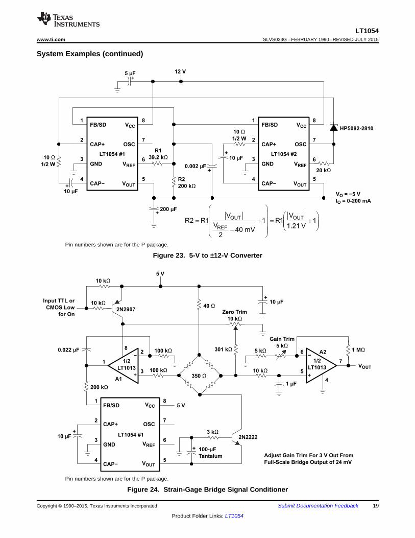
System Examples (continued)
Pin numbers shown are for the P package.
Figure 23. 5-V to ±12-V Converter
Pin numbers shown are for the P package.
Figure 24. Strain-Gage Bridge Signal Conditioner
Copyright © 1990–2015, Texas Instruments Incorporated Submit Documentation Feedback 19
Product Folder Links: LT1054
1N58171N914
2N2219
R2
125 kΩ
R2
125 kΩ
R1
20 kΩ
1N914
(All)
VI
3.5 V to 5.5 V
FB/SD
CAP+
GND
CAP−
VCC
OSC
VREF
VOUT
LT1054
+
VREF
LTC1044
VOUT
OSC
VCC
CAP−
GND
CAP+
FB/SD
VO
1 μF
1 μF
3 kΩ100 μF
5 μF
10 μF
20 kΩ
0.002 μF
VI = 3.5 V to 5.5 V
VO = 5 V
IO MAX = 50 mA
+
1
2
4
8
7
6
5
3
1
2
4
8
7
6
5
3
+
+
+
−
+
OUT OUT
REF
V VR2 R1 1 R1 1
V 1.21 V40 mV
2
æ öç ÷ æ ö
= + = +ç ÷ ç ÷ç ÷ç ÷ è ø-ç ÷è ø
LT1054SLVS033G –FEBRUARY 1990–REVISED JULY 2015 www.ti.com
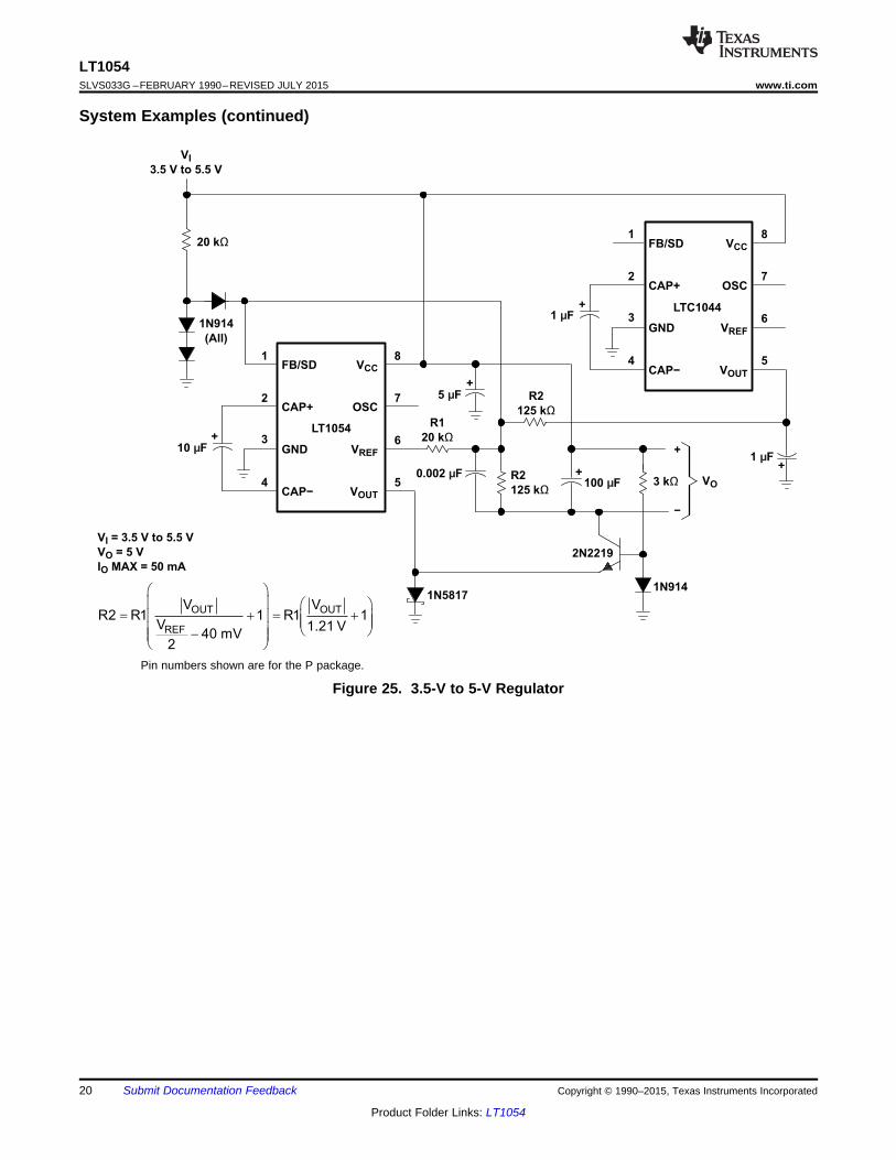
System Examples (continued)
Pin numbers shown are for the P package.
Figure 25. 3.5-V to 5-V Regulator
20 Submit Documentation Feedback Copyright © 1990–2015, Texas Instruments Incorporated
Product Folder Links: LT1054
AD558Digital
Input
VO = −VI (Programmed)
LT1004-2.52.5 V
15 V
LT1054
VOUT
VREF
OSC
VCC
CAP−
GND
CAP+
FB/SD
100 μF
10 μF
20 kΩ
20 kΩ
5 μF+
+
1
2
4
8
7
6
5
3
+
16
11
1514 13 12
VCC
OSC
VREF
VOUT
HP5082-2810
VO = −5 V
IO = 0-200 mA
R2
200 kΩ
R1
39.2 kΩ
12 V
FB/SD
CAP+
GND
CAP−
LT1054 #2
VCC
OSC
VREF
VOUT
LT1054 #1
CAP−
GND
CAP+
FB/SD
5 μF
10 Ω
1/2 W
10 μF
0.002 μF
10 μF
20 kΩ
200 μF
10 Ω
1/2 W
+
1
2
4
8
7
6
5
3
1
2
4
8
7
6
5
3
+
+
+
+
OUT OUT
REF
V VR2 R1 1 R1 1
V 1.21 V40 mV
2
æ öç ÷ æ ö
= + = +ç ÷ ç ÷ç ÷ç ÷ è ø-ç ÷è ø
LT1054www.ti.com SLVS033G –FEBRUARY 1990–REVISED JULY 2015
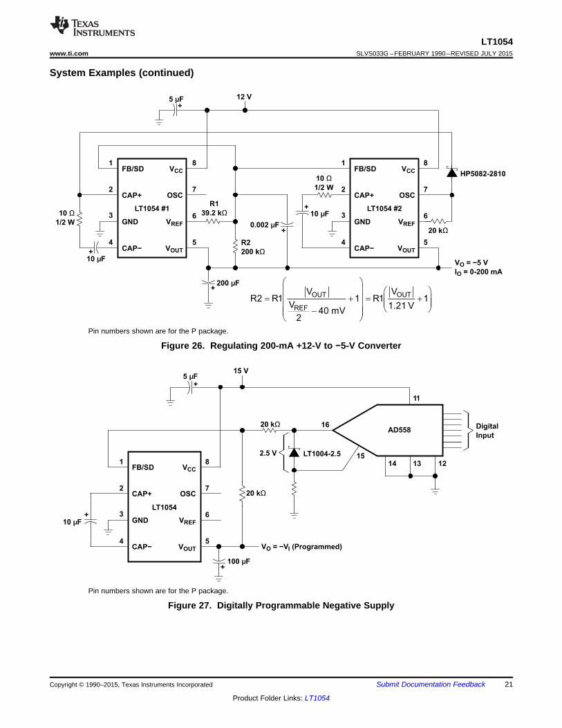
System Examples (continued)
Pin numbers shown are for the P package.
Figure 26. Regulating 200-mA +12-V to −5-V Converter
Pin numbers shown are for the P package.
Figure 27. Digitally Programmable Negative Supply
Copyright © 1990–2015, Texas Instruments Incorporated Submit Documentation Feedback 21
Product Folder Links: LT1054
−VO
1N4001
1N4001
R2
1 MΩ
R1
60 kΩ
VI
3.5 V to 15 V
LT1054
VOUT
VREF
OSC
VCC
CAP−
GND
CAP+
FB/SD
10 μF
100 μF
100 μF
2μF
10 Fμ
0.002 μF
VI = 3.5 V to 15 V
VO MAX ≈ 2 VIN + (VL + 2 VDiode)
VL = LT1054 Voltage Loss
1
2
4
8
7
6
5
3
+
+
+
+
+
OUT OUT
REF
V VR2 R1 1 R1 1
V 1.21 V40 mV
2
æ öç ÷ æ ö
= + = +ç ÷ ç ÷ç ÷ç ÷ è ø-ç ÷è ø
5 V
VI = 5 V
1N5817VO
8 V
LT1054
VOUT
VREF
OSC
VCC
CAP−
GND
CAP+
FB/SD
10 kΩ10 kΩ
0.1 μF
10 kΩ
5.5 kΩ
2.5 kΩ
100 μF 0.03 μF
10 μF
2μF
1/2
LT1013
1N5817
50 kΩ
+
1
2
4
8
7
6
5
3
+
+
−
+
LT1054SLVS033G –FEBRUARY 1990–REVISED JULY 2015 www.ti.com
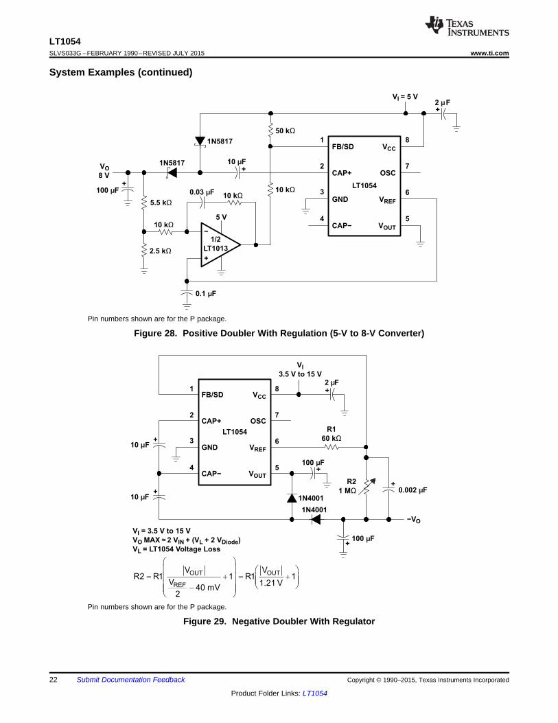
System Examples (continued)
Pin numbers shown are for the P package.
Figure 28. Positive Doubler With Regulation (5-V to 8-V Converter)
Pin numbers shown are for the P package.
Figure 29. Negative Doubler With Regulator
22 Submit Documentation Feedback Copyright © 1990–2015, Texas Instruments Incorporated
Product Folder Links: LT1054
R1
CIN
Load
VOUT
VREF
OSC
VCC
CAP−
GND
CAP+
FB/SD
VIN
VOUT
COUT
+
+
1
2
3
4
LT1054
8
7
6
5
( )OUT
OUT
VR1
I
b£
LT1054www.ti.com SLVS033G –FEBRUARY 1990–REVISED JULY 2015
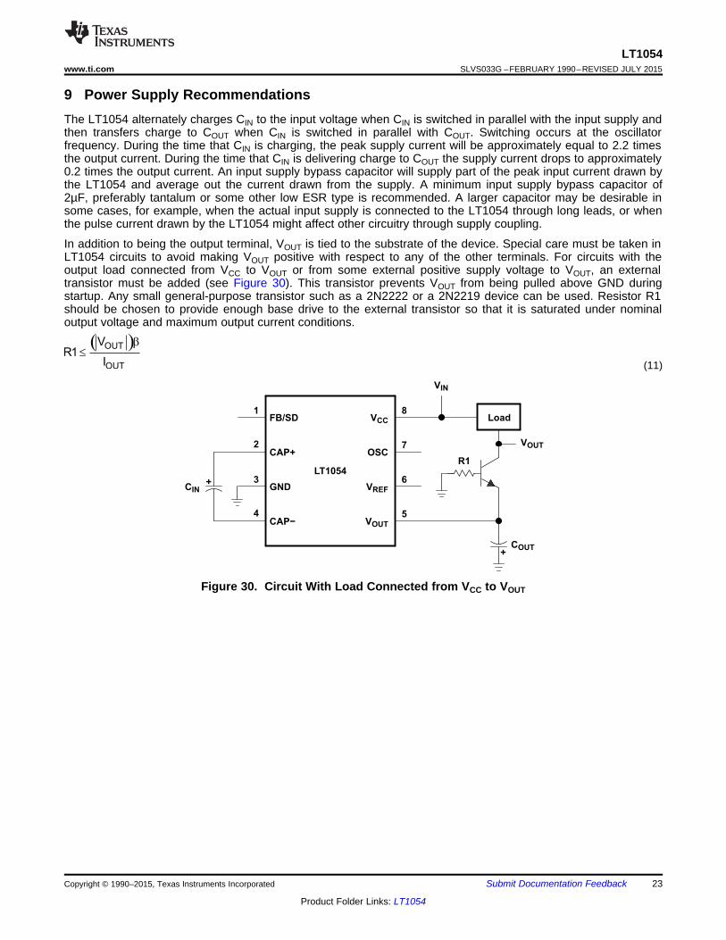
9 Power Supply RecommendationsThe LT1054 alternately charges CIN to the input voltage when CIN is switched in parallel with the input supply andthen transfers charge to COUT when CIN is switched in parallel with COUT. Switching occurs at the oscillatorfrequency. During the time that CIN is charging, the peak supply current will be approximately equal to 2.2 timesthe output current. During the time that CIN is delivering charge to COUT the supply current drops to approximately0.2 times the output current. An input supply bypass capacitor will supply part of the peak input current drawn bythe LT1054 and average out the current drawn from the supply. A minimum input supply bypass capacitor of2µF, preferably tantalum or some other low ESR type is recommended. A larger capacitor may be desirable insome cases, for example, when the actual input supply is connected to the LT1054 through long leads, or whenthe pulse current drawn by the LT1054 might affect other circuitry through supply coupling.
In addition to being the output terminal, VOUT is tied to the substrate of the device. Special care must be taken inLT1054 circuits to avoid making VOUT positive with respect to any of the other terminals. For circuits with theoutput load connected from VCC to VOUT or from some external positive supply voltage to VOUT, an externaltransistor must be added (see Figure 30). This transistor prevents VOUT from being pulled above GND duringstartup. Any small general-purpose transistor such as a 2N2222 or a 2N2219 device can be used. Resistor R1should be chosen to provide enough base drive to the external transistor so that it is saturated under nominaloutput voltage and maximum output current conditions.
(11)
Figure 30. Circuit With Load Connected from VCC to VOUT
Copyright © 1990–2015, Texas Instruments Incorporated Submit Documentation Feedback 23
Product Folder Links: LT1054
2.0 PF
FB/SD 1
CAP+ 2
GND 3
&$3í 4
8 VCC
7 OSC 6 VREF
5 VOUT
Ground
Positive Supply
100 PF
Ground
R2
0.002 PF
R1
10 PF
Ground
LT1054SLVS033G –FEBRUARY 1990–REVISED JULY 2015 www.ti.com
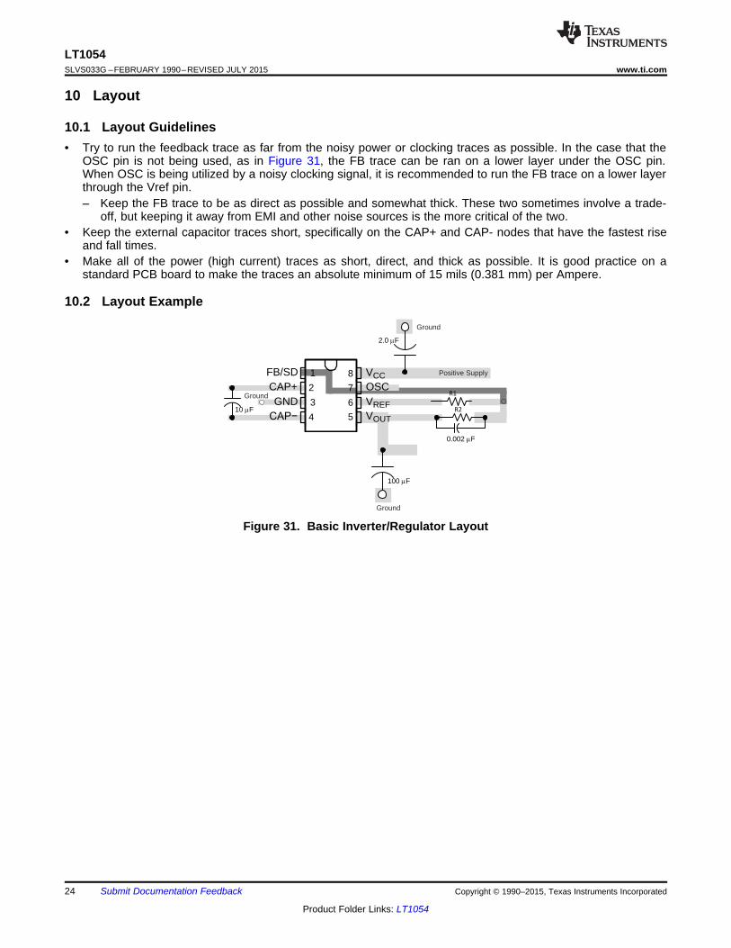
10 Layout
10.1 Layout Guidelines• Try to run the feedback trace as far from the noisy power or clocking traces as possible. In the case that the
OSC pin is not being used, as in Figure 31, the FB trace can be ran on a lower layer under the OSC pin.When OSC is being utilized by a noisy clocking signal, it is recommended to run the FB trace on a lower layerthrough the Vref pin.– Keep the FB trace to be as direct as possible and somewhat thick. These two sometimes involve a trade-
off, but keeping it away from EMI and other noise sources is the more critical of the two.• Keep the external capacitor traces short, specifically on the CAP+ and CAP- nodes that have the fastest rise
and fall times.• Make all of the power (high current) traces as short, direct, and thick as possible. It is good practice on a
standard PCB board to make the traces an absolute minimum of 15 mils (0.381 mm) per Ampere.
10.2 Layout Example
Figure 31. Basic Inverter/Regulator Layout
24 Submit Documentation Feedback Copyright © 1990–2015, Texas Instruments Incorporated
Product Folder Links: LT1054
LT1054www.ti.com SLVS033G –FEBRUARY 1990–REVISED JULY 2015
11 Device and Documentation Support
11.1 Community ResourcesThe following links connect to TI community resources. Linked contents are provided "AS IS" by the respectivecontributors. They do not constitute TI specifications and do not necessarily reflect TI's views; see TI's Terms ofUse.
TI E2E™ Online Community TI's Engineer-to-Engineer (E2E) Community. Created to foster collaborationamong engineers. At e2e.ti.com, you can ask questions, share knowledge, explore ideas and helpsolve problems with fellow engineers.
Design Support TI's Design Support Quickly find helpful E2E forums along with design support tools andcontact information for technical support.
11.2 TrademarksE2E is a trademark of Texas Instruments.All other trademarks are the property of their respective owners.
11.3 Electrostatic Discharge CautionThese devices have limited built-in ESD protection. The leads should be shorted together or the device placed in conductive foamduring storage or handling to prevent electrostatic damage to the MOS gates.
11.4 GlossarySLYZ022 — TI Glossary.
This glossary lists and explains terms, acronyms, and definitions.
12 Mechanical, Packaging, and Orderable InformationThe following pages include mechanical, packaging, and orderable information. This information is the mostcurrent data available for the designated devices. This data is subject to change without notice and revision ofthis document. For browser-based versions of this data sheet, refer to the left-hand navigation.
Copyright © 1990–2015, Texas Instruments Incorporated Submit Documentation Feedback 25
Product Folder Links: LT1054
PACKAGE OPTION ADDENDUM
www.ti.com 17-Mar-2017
Addendum-Page 1
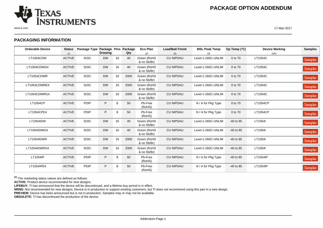
PACKAGING INFORMATION
Orderable Device Status(1)
Package Type PackageDrawing
Pins PackageQty
Eco Plan(2)
Lead/Ball Finish(6)
MSL Peak Temp(3)
Op Temp (°C) Device Marking(4/5)
Samples
LT1054CDW ACTIVE SOIC DW 16 40 Green (RoHS& no Sb/Br)
CU NIPDAU Level-1-260C-UNLIM 0 to 70 LT1054C
LT1054CDWG4 ACTIVE SOIC DW 16 40 Green (RoHS& no Sb/Br)
CU NIPDAU Level-1-260C-UNLIM 0 to 70 LT1054C
LT1054CDWR ACTIVE SOIC DW 16 2000 Green (RoHS& no Sb/Br)
CU NIPDAU Level-1-260C-UNLIM 0 to 70 LT1054C
LT1054CDWRE4 ACTIVE SOIC DW 16 2000 Green (RoHS& no Sb/Br)
CU NIPDAU Level-1-260C-UNLIM 0 to 70 LT1054C
LT1054CDWRG4 ACTIVE SOIC DW 16 2000 Green (RoHS& no Sb/Br)
CU NIPDAU Level-1-260C-UNLIM 0 to 70 LT1054C
LT1054CP ACTIVE PDIP P 8 50 Pb-Free(RoHS)
CU NIPDAU N / A for Pkg Type 0 to 70 LT1054CP
LT1054CPE4 ACTIVE PDIP P 8 50 Pb-Free(RoHS)
CU NIPDAU N / A for Pkg Type 0 to 70 LT1054CP
LT1054IDW ACTIVE SOIC DW 16 40 Green (RoHS& no Sb/Br)
CU NIPDAU Level-1-260C-UNLIM -40 to 85 LT1054I
LT1054IDWG4 ACTIVE SOIC DW 16 40 Green (RoHS& no Sb/Br)
CU NIPDAU Level-1-260C-UNLIM -40 to 85 LT1054I
LT1054IDWR ACTIVE SOIC DW 16 2000 Green (RoHS& no Sb/Br)
CU NIPDAU Level-1-260C-UNLIM -40 to 85 LT1054I
LT1054IDWRG4 ACTIVE SOIC DW 16 2000 Green (RoHS& no Sb/Br)
CU NIPDAU Level-1-260C-UNLIM -40 to 85 LT1054I
LT1054IP ACTIVE PDIP P 8 50 Pb-Free(RoHS)
CU NIPDAU N / A for Pkg Type -40 to 85 LT1054IP
LT1054IPE4 ACTIVE PDIP P 8 50 Pb-Free(RoHS)
CU NIPDAU N / A for Pkg Type -40 to 85 LT1054IP
(1) The marketing status values are defined as follows:ACTIVE: Product device recommended for new designs.LIFEBUY: TI has announced that the device will be discontinued, and a lifetime-buy period is in effect.NRND: Not recommended for new designs. Device is in production to support existing customers, but TI does not recommend using this part in a new design.PREVIEW: Device has been announced but is not in production. Samples may or may not be available.OBSOLETE: TI has discontinued the production of the device.
PACKAGE OPTION ADDENDUM
www.ti.com 17-Mar-2017
Addendum-Page 2
(2) Eco Plan - The planned eco-friendly classification: Pb-Free (RoHS), Pb-Free (RoHS Exempt), or Green (RoHS & no Sb/Br) - please check http://www.ti.com/productcontent for the latest availabilityinformation and additional product content details.TBD: The Pb-Free/Green conversion plan has not been defined.Pb-Free (RoHS): TI's terms "Lead-Free" or "Pb-Free" mean semiconductor products that are compatible with the current RoHS requirements for all 6 substances, including the requirement thatlead not exceed 0.1% by weight in homogeneous materials. Where designed to be soldered at high temperatures, TI Pb-Free products are suitable for use in specified lead-free processes.Pb-Free (RoHS Exempt): This component has a RoHS exemption for either 1) lead-based flip-chip solder bumps used between the die and package, or 2) lead-based die adhesive used betweenthe die and leadframe. The component is otherwise considered Pb-Free (RoHS compatible) as defined above.Green (RoHS & no Sb/Br): TI defines "Green" to mean Pb-Free (RoHS compatible), and free of Bromine (Br) and Antimony (Sb) based flame retardants (Br or Sb do not exceed 0.1% by weightin homogeneous material)
(3) MSL, Peak Temp. - The Moisture Sensitivity Level rating according to the JEDEC industry standard classifications, and peak solder temperature.
(4) There may be additional marking, which relates to the logo, the lot trace code information, or the environmental category on the device.
(5) Multiple Device Markings will be inside parentheses. Only one Device Marking contained in parentheses and separated by a "~" will appear on a device. If a line is indented then it is a continuationof the previous line and the two combined represent the entire Device Marking for that device.
(6) Lead/Ball Finish - Orderable Devices may have multiple material finish options. Finish options are separated by a vertical ruled line. Lead/Ball Finish values may wrap to two lines if the finishvalue exceeds the maximum column width.
Important Information and Disclaimer:The information provided on this page represents TI's knowledge and belief as of the date that it is provided. TI bases its knowledge and belief on informationprovided by third parties, and makes no representation or warranty as to the accuracy of such information. Efforts are underway to better integrate information from third parties. TI has taken andcontinues to take reasonable steps to provide representative and accurate information but may not have conducted destructive testing or chemical analysis on incoming materials and chemicals.TI and TI suppliers consider certain information to be proprietary, and thus CAS numbers and other limited information may not be available for release.
In no event shall TI's liability arising out of such information exceed the total purchase price of the TI part(s) at issue in this document sold by TI to Customer on an annual basis.
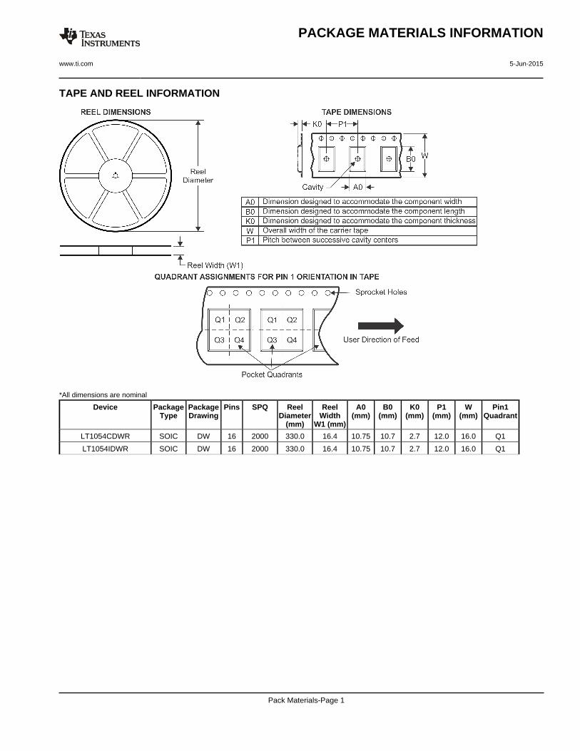
TAPE AND REEL INFORMATION
*All dimensions are nominal
Device PackageType
PackageDrawing
Pins SPQ ReelDiameter
(mm)
ReelWidth
W1 (mm)
A0(mm)
B0(mm)
K0(mm)
P1(mm)
W(mm)
Pin1Quadrant
LT1054CDWR SOIC DW 16 2000 330.0 16.4 10.75 10.7 2.7 12.0 16.0 Q1
LT1054IDWR SOIC DW 16 2000 330.0 16.4 10.75 10.7 2.7 12.0 16.0 Q1
PACKAGE MATERIALS INFORMATION
www.ti.com 5-Jun-2015
Pack Materials-Page 1
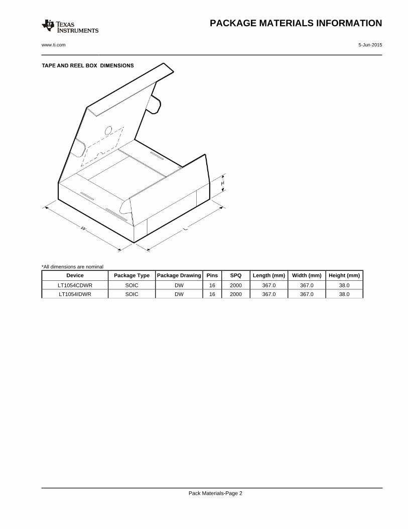
*All dimensions are nominal
Device Package Type Package Drawing Pins SPQ Length (mm) Width (mm) Height (mm)
LT1054CDWR SOIC DW 16 2000 367.0 367.0 38.0
LT1054IDWR SOIC DW 16 2000 367.0 367.0 38.0
PACKAGE MATERIALS INFORMATION
www.ti.com 5-Jun-2015
Pack Materials-Page 2
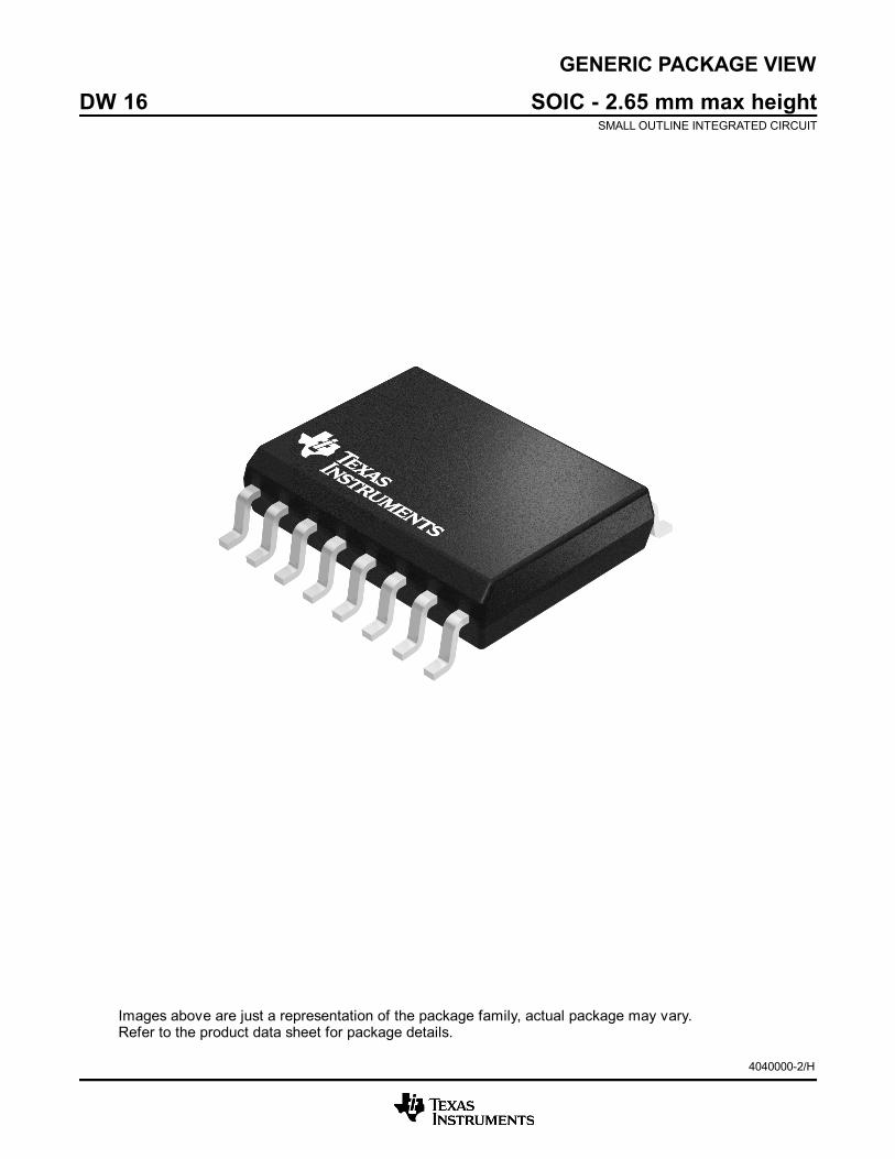
GENERIC PACKAGE VIEW
Images above are just a representation of the package family, actual package may vary.Refer to the product data sheet for package details.
DW 16 SOIC - 2.65 mm max heightSMALL OUTLINE INTEGRATED CIRCUIT
4040000-2/H
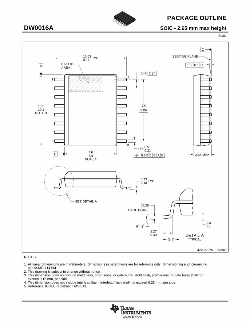
www.ti.com
PACKAGE OUTLINE
C
TYP10.639.97
2.65 MAX
14X 1.27
16X 0.510.31
2X8.89
TYP0.330.10
0 - 80.30.1
(1.4)
0.25GAGE PLANE
1.270.40
A
NOTE 3
10.510.1
BNOTE 4
7.67.4
4220721/A 07/2016
SOIC - 2.65 mm max heightDW0016ASOIC
NOTES: 1. All linear dimensions are in millimeters. Dimensions in parenthesis are for reference only. Dimensioning and tolerancing per ASME Y14.5M. 2. This drawing is subject to change without notice. 3. This dimension does not include mold flash, protrusions, or gate burrs. Mold flash, protrusions, or gate burrs shall not exceed 0.15 mm, per side. 4. This dimension does not include interlead flash. Interlead flash shall not exceed 0.25 mm, per side.5. Reference JEDEC registration MS-013.
1 16
0.25 C A B
98
PIN 1 IDAREA
SEATING PLANE
0.1 C
SEE DETAIL A
DETAIL ATYPICAL
SCALE 1.500
www.ti.com
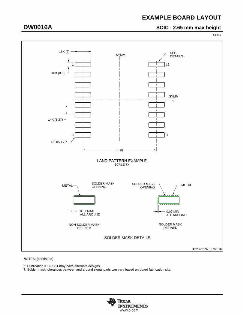
EXAMPLE BOARD LAYOUT
0.07 MAXALL AROUND
0.07 MINALL AROUND
(9.3)
14X (1.27)
R0.05 TYP
16X (2)
16X (0.6)
4220721/A 07/2016
SOIC - 2.65 mm max heightDW0016ASOIC
NOTES: (continued) 6. Publication IPC-7351 may have alternate designs. 7. Solder mask tolerances between and around signal pads can vary based on board fabrication site.
METAL SOLDER MASKOPENING
NON SOLDER MASKDEFINED
SOLDER MASK DETAILS
OPENINGSOLDER MASK METAL
SOLDER MASKDEFINED
LAND PATTERN EXAMPLESCALE:7X
SYMM
1
8 9
16
SEEDETAILS
SYMM
www.ti.com
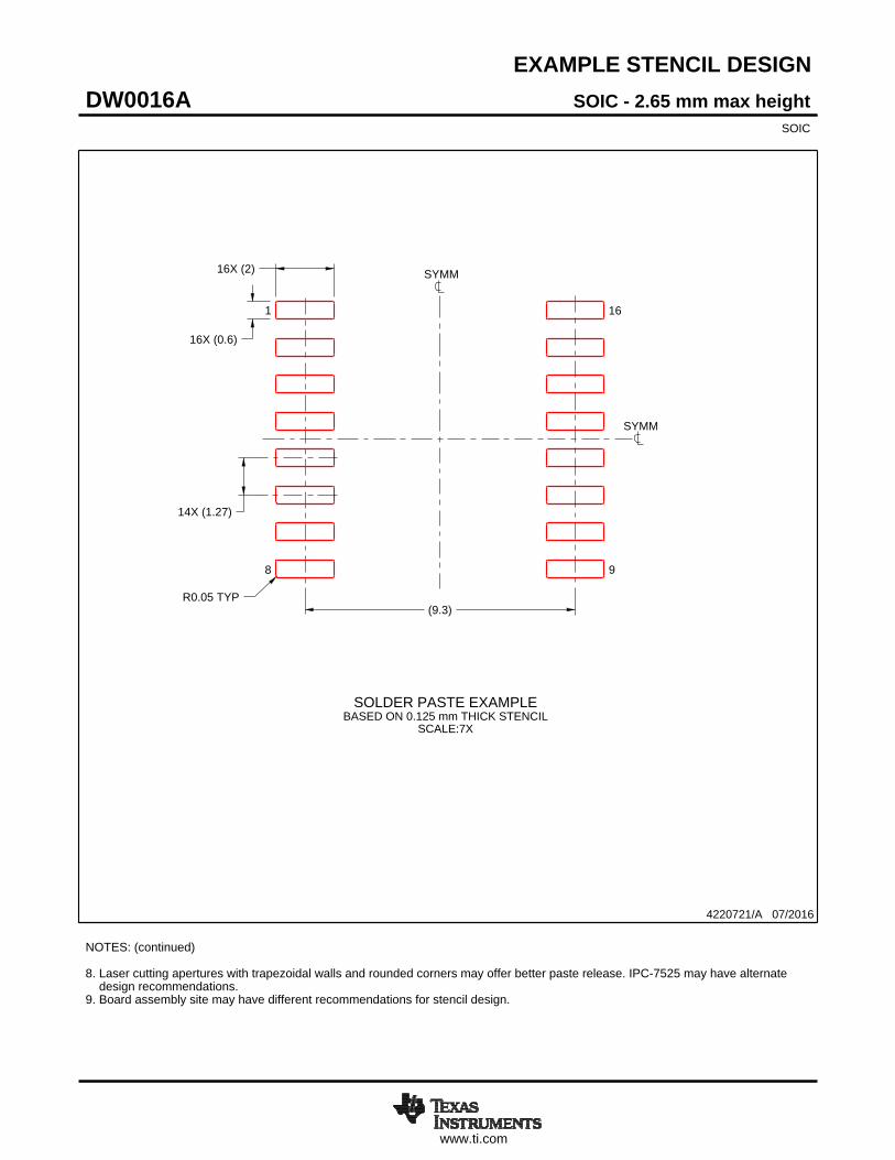
EXAMPLE STENCIL DESIGN
R0.05 TYP
16X (2)
16X (0.6)
14X (1.27)
(9.3)
4220721/A 07/2016
SOIC - 2.65 mm max heightDW0016ASOIC
NOTES: (continued) 8. Laser cutting apertures with trapezoidal walls and rounded corners may offer better paste release. IPC-7525 may have alternate design recommendations. 9. Board assembly site may have different recommendations for stencil design.
SOLDER PASTE EXAMPLEBASED ON 0.125 mm THICK STENCIL
SCALE:7X
SYMM
SYMM
1
8 9
16
IMPORTANT NOTICE
Texas Instruments Incorporated (TI) reserves the right to make corrections, enhancements, improvements and other changes to itssemiconductor products and services per JESD46, latest issue, and to discontinue any product or service per JESD48, latest issue. Buyersshould obtain the latest relevant information before placing orders and should verify that such information is current and complete.TI’s published terms of sale for semiconductor products (http://www.ti.com/sc/docs/stdterms.htm) apply to the sale of packaged integratedcircuit products that TI has qualified and released to market. Additional terms may apply to the use or sale of other types of TI products andservices.Reproduction of significant portions of TI information in TI data sheets is permissible only if reproduction is without alteration and isaccompanied by all associated warranties, conditions, limitations, and notices. TI is not responsible or liable for such reproduceddocumentation. Information of third parties may be subject to additional restrictions. Resale of TI products or services with statementsdifferent from or beyond the parameters stated by TI for that product or service voids all express and any implied warranties for theassociated TI product or service and is an unfair and deceptive business practice. TI is not responsible or liable for any such statements.Buyers and others who are developing systems that incorporate TI products (collectively, “Designers”) understand and agree that Designersremain responsible for using their independent analysis, evaluation and judgment in designing their applications and that Designers havefull and exclusive responsibility to assure the safety of Designers' applications and compliance of their applications (and of all TI productsused in or for Designers’ applications) with all applicable regulations, laws and other applicable requirements. Designer represents that, withrespect to their applications, Designer has all the necessary expertise to create and implement safeguards that (1) anticipate dangerousconsequences of failures, (2) monitor failures and their consequences, and (3) lessen the likelihood of failures that might cause harm andtake appropriate actions. Designer agrees that prior to using or distributing any applications that include TI products, Designer willthoroughly test such applications and the functionality of such TI products as used in such applications.TI’s provision of technical, application or other design advice, quality characterization, reliability data or other services or information,including, but not limited to, reference designs and materials relating to evaluation modules, (collectively, “TI Resources”) are intended toassist designers who are developing applications that incorporate TI products; by downloading, accessing or using TI Resources in anyway, Designer (individually or, if Designer is acting on behalf of a company, Designer’s company) agrees to use any particular TI Resourcesolely for this purpose and subject to the terms of this Notice.TI’s provision of TI Resources does not expand or otherwise alter TI’s applicable published warranties or warranty disclaimers for TIproducts, and no additional obligations or liabilities arise from TI providing such TI Resources. TI reserves the right to make corrections,enhancements, improvements and other changes to its TI Resources. TI has not conducted any testing other than that specificallydescribed in the published documentation for a particular TI Resource.Designer is authorized to use, copy and modify any individual TI Resource only in connection with the development of applications thatinclude the TI product(s) identified in such TI Resource. NO OTHER LICENSE, EXPRESS OR IMPLIED, BY ESTOPPEL OR OTHERWISETO ANY OTHER TI INTELLECTUAL PROPERTY RIGHT, AND NO LICENSE TO ANY TECHNOLOGY OR INTELLECTUAL PROPERTYRIGHT OF TI OR ANY THIRD PARTY IS GRANTED HEREIN, including but not limited to any patent right, copyright, mask work right, orother intellectual property right relating to any combination, machine, or process in which TI products or services are used. Informationregarding or referencing third-party products or services does not constitute a license to use such products or services, or a warranty orendorsement thereof. Use of TI Resources may require a license from a third party under the patents or other intellectual property of thethird party, or a license from TI under the patents or other intellectual property of TI.TI RESOURCES ARE PROVIDED “AS IS” AND WITH ALL FAULTS. TI DISCLAIMS ALL OTHER WARRANTIES ORREPRESENTATIONS, EXPRESS OR IMPLIED, REGARDING RESOURCES OR USE THEREOF, INCLUDING BUT NOT LIMITED TOACCURACY OR COMPLETENESS, TITLE, ANY EPIDEMIC FAILURE WARRANTY AND ANY IMPLIED WARRANTIES OFMERCHANTABILITY, FITNESS FOR A PARTICULAR PURPOSE, AND NON-INFRINGEMENT OF ANY THIRD PARTY INTELLECTUALPROPERTY RIGHTS. TI SHALL NOT BE LIABLE FOR AND SHALL NOT DEFEND OR INDEMNIFY DESIGNER AGAINST ANY CLAIM,INCLUDING BUT NOT LIMITED TO ANY INFRINGEMENT CLAIM THAT RELATES TO OR IS BASED ON ANY COMBINATION OFPRODUCTS EVEN IF DESCRIBED IN TI RESOURCES OR OTHERWISE. IN NO EVENT SHALL TI BE LIABLE FOR ANY ACTUAL,DIRECT, SPECIAL, COLLATERAL, INDIRECT, PUNITIVE, INCIDENTAL, CONSEQUENTIAL OR EXEMPLARY DAMAGES INCONNECTION WITH OR ARISING OUT OF TI RESOURCES OR USE THEREOF, AND REGARDLESS OF WHETHER TI HAS BEENADVISED OF THE POSSIBILITY OF SUCH DAMAGES.Unless TI has explicitly designated an individual product as meeting the requirements of a particular industry standard (e.g., ISO/TS 16949and ISO 26262), TI is not responsible for any failure to meet such industry standard requirements.Where TI specifically promotes products as facilitating functional safety or as compliant with industry functional safety standards, suchproducts are intended to help enable customers to design and create their own applications that meet applicable functional safety standardsand requirements. Using products in an application does not by itself establish any safety features in the application. Designers mustensure compliance with safety-related requirements and standards applicable to their applications. Designer may not use any TI products inlife-critical medical equipment unless authorized officers of the parties have executed a special contract specifically governing such use.Life-critical medical equipment is medical equipment where failure of such equipment would cause serious bodily injury or death (e.g., lifesupport, pacemakers, defibrillators, heart pumps, neurostimulators, and implantables). Such equipment includes, without limitation, allmedical devices identified by the U.S. Food and Drug Administration as Class III devices and equivalent classifications outside the U.S.TI may expressly designate certain products as completing a particular qualification (e.g., Q100, Military Grade, or Enhanced Product).Designers agree that it has the necessary expertise to select the product with the appropriate qualification designation for their applicationsand that proper product selection is at Designers’ own risk. Designers are solely responsible for compliance with all legal and regulatoryrequirements in connection with such selection.Designer will fully indemnify TI and its representatives against any damages, costs, losses, and/or liabilities arising out of Designer’s non-compliance with the terms and provisions of this Notice.
Mailing Address: Texas Instruments, Post Office Box 655303, Dallas, Texas 75265Copyright © 2017, Texas Instruments Incorporated