LMZ14202 2A SIMPLE SWITCHER® Power Module with … Sheets/Texas Instruments PDFs... · η...
20
LMZ14202 LMZ14202 2A SIMPLE SWITCHER® Power Module with 42V Maximum Input Voltage Literature Number: SNVS648D
Transcript of LMZ14202 2A SIMPLE SWITCHER® Power Module with … Sheets/Texas Instruments PDFs... · η...
LMZ14202
LMZ14202 2A SIMPLE SWITCHER® Power Module with 42V Maximum Input Voltage
Literature Number: SNVS648D
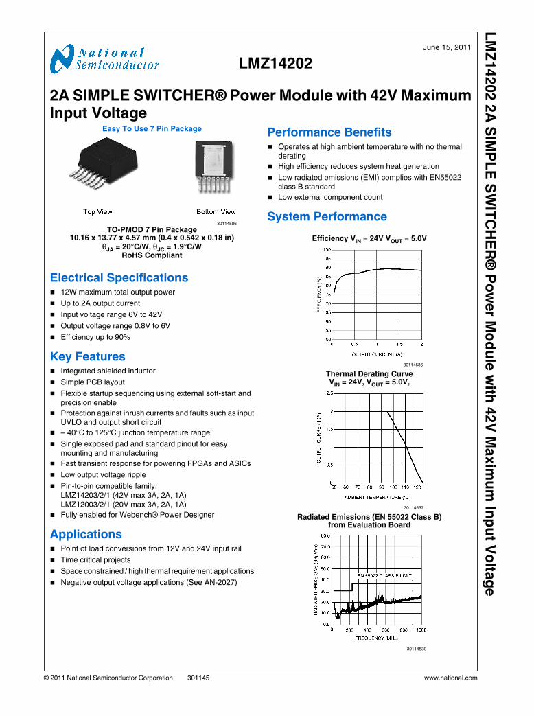
LMZ14202June 15, 2011
2A SIMPLE SWITCHER® Power Module with 42V MaximumInput Voltage
Easy To Use 7 Pin Package
30114586
TO-PMOD 7 Pin Package10.16 x 13.77 x 4.57 mm (0.4 x 0.542 x 0.18 in)
θJA = 20°C/W, θJC = 1.9°C/WRoHS Compliant
Electrical Specifications 12W maximum total output power
Up to 2A output current
Input voltage range 6V to 42V
Output voltage range 0.8V to 6V
Efficiency up to 90%
Key Features Integrated shielded inductor
Simple PCB layout
Flexible startup sequencing using external soft-start andprecision enable
Protection against inrush currents and faults such as inputUVLO and output short circuit
– 40°C to 125°C junction temperature range
Single exposed pad and standard pinout for easymounting and manufacturing
Fast transient response for powering FPGAs and ASICs
Low output voltage ripple
Pin-to-pin compatible family:LMZ14203/2/1 (42V max 3A, 2A, 1A)LMZ12003/2/1 (20V max 3A, 2A, 1A)
Fully enabled for Webench® Power Designer
Applications Point of load conversions from 12V and 24V input rail
Time critical projects
Space constrained / high thermal requirement applications
Negative output voltage applications (See AN-2027)
Performance Benefits Operates at high ambient temperature with no thermal
derating
High efficiency reduces system heat generation
Low radiated emissions (EMI) complies with EN55022class B standard
Low external component count
System Performance
Efficiency VIN = 24V VOUT = 5.0V
30114536
Thermal Derating CurveVIN = 24V, VOUT = 5.0V,
30114537
Radiated Emissions (EN 55022 Class B)from Evaluation Board
30114539
© 2011 National Semiconductor Corporation 301145 www.national.com
LM
Z14202 2
A S
IMP
LE
SW
ITC
HE
R®
Po
wer M
od
ule
with
42V
Maxim
um
Inp
ut V
olta
ge
Simplified Application Schematic
30114501
Connection Diagram
30114502
Top View7-Lead TO-PMOD
Ordering Information
Order Number Package Type NSC Package Drawing Supplied As
LMZ14202TZ-ADJ TO-PMOD-7 TZA07A 250 Units in Tape and Reel
LMZ14202TZX-ADJ TO-PMOD-7 TZA07A 500 Units in Tape and Reel
LMZ14202TZE-ADJ TO-PMOD-7 TZA07A 45 Units in a Rail
Pin Descriptions
Pin Name Description
1 VIN Supply input — Nominal operating range is 6V to 42V . A small amount of internal capacitance is contained within the
package assembly. Additional external input capacitance is required between this pin and exposed pad.
2 RON On Time Resistor — An external resistor from VIN to this pin sets the on-time of the application. Typical values range
from 25k to 124k ohms.
3 EN Enable — Input to the precision enable comparator. Rising threshold is 1.18V nominal; 90 mV hysteresis nominal.
Maximum recommended input level is 6.5V.
4 GND Ground — Reference point for all stated voltages. Must be externally connected to EP.
5 SS Soft-Start — An internal 8 µA current source charges an external capacitor to produce the soft-start function. This node
is discharged at 200 µA during disable, over-current, thermal shutdown and internal UVLO conditions.
www.national.com 2
LM
Z14202
Pin Name Description
6 FB Feedback — Internally connected to the regulation, over-voltage, and short-circuit comparators. The regulation
reference point is 0.8V at this input pin. Connected the feedback resistor divider between the output and ground to set
the output voltage.
7 VOUT Output Voltage — Output from the internal inductor. Connect the output capacitor between this pin and exposed pad.
EP EP Exposed Pad — Internally connected to pin 4. Used to dissipate heat from the package during operation. Must be
electrically connected to pin 4 external to the package.
3 www.national.com
LM
Z14202
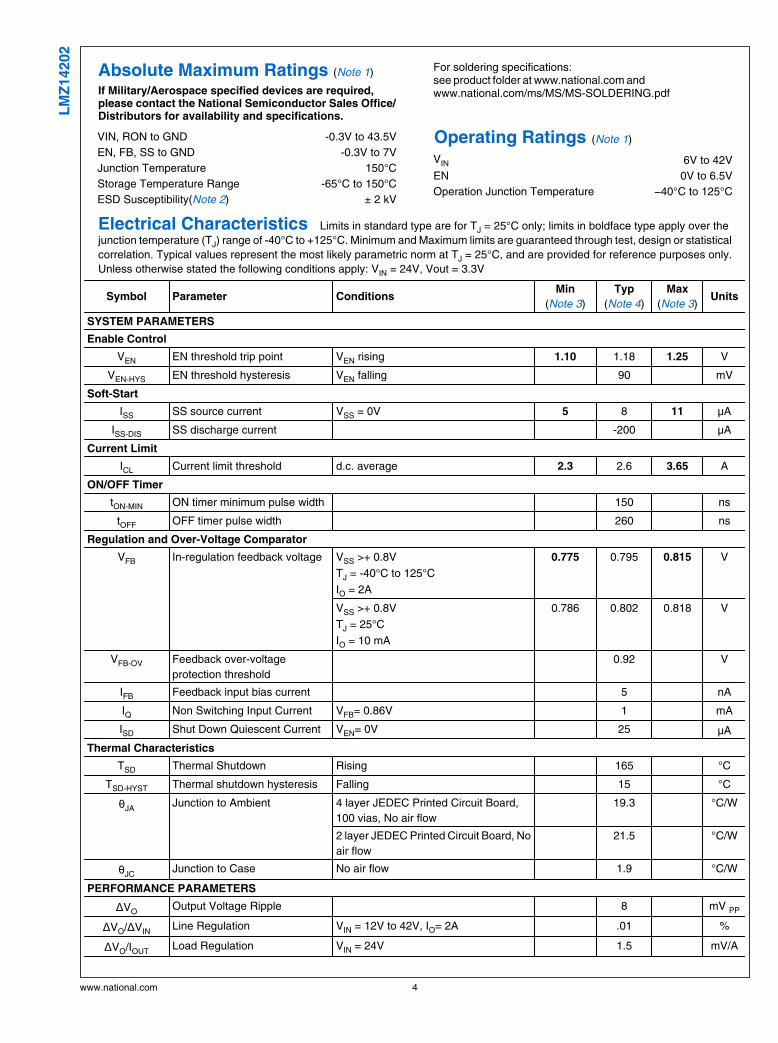
Absolute Maximum Ratings (Note 1)
If Military/Aerospace specified devices are required,please contact the National Semiconductor Sales Office/Distributors for availability and specifications.
VIN, RON to GND -0.3V to 43.5V
EN, FB, SS to GND -0.3V to 7V
Junction Temperature 150°C
Storage Temperature Range -65°C to 150°C
ESD Susceptibility(Note 2) ± 2 kV
For soldering specifications:see product folder at www.national.com andwww.national.com/ms/MS/MS-SOLDERING.pdf
Operating Ratings (Note 1)
VIN 6V to 42V
EN 0V to 6.5V
Operation Junction Temperature −40°C to 125°C
Electrical Characteristics Limits in standard type are for TJ = 25°C only; limits in boldface type apply over the
junction temperature (TJ) range of -40°C to +125°C. Minimum and Maximum limits are guaranteed through test, design or statistical
correlation. Typical values represent the most likely parametric norm at TJ = 25°C, and are provided for reference purposes only.
Unless otherwise stated the following conditions apply: VIN = 24V, Vout = 3.3V
Symbol Parameter ConditionsMin
(Note 3)
Typ
(Note 4)
Max
(Note 3)Units
SYSTEM PARAMETERS
Enable Control
VEN EN threshold trip point VEN rising 1.10 1.18 1.25 V
VEN-HYS EN threshold hysteresis VEN falling 90 mV
Soft-Start
ISS SS source current VSS = 0V 5 8 11 µA
ISS-DIS SS discharge current -200 µA
Current Limit
ICL Current limit threshold d.c. average 2.3 2.6 3.65 A
ON/OFF Timer
tON-MIN ON timer minimum pulse width 150 ns
tOFF OFF timer pulse width 260 ns
Regulation and Over-Voltage Comparator
VFB In-regulation feedback voltage VSS >+ 0.8V
TJ = -40°C to 125°C
IO = 2A
0.775 0.795 0.815 V
VSS >+ 0.8V
TJ = 25°C
IO = 10 mA
0.786 0.802 0.818 V
VFB-OV Feedback over-voltage
protection threshold
0.92 V
IFB Feedback input bias current 5 nA
IQ Non Switching Input Current VFB= 0.86V 1 mA
ISD Shut Down Quiescent Current VEN= 0V 25 μA
Thermal Characteristics
TSD Thermal Shutdown Rising 165 °C
TSD-HYST Thermal shutdown hysteresis Falling 15 °C
θJAJunction to Ambient 4 layer JEDEC Printed Circuit Board,
100 vias, No air flow
19.3 °C/W
2 layer JEDEC Printed Circuit Board, No
air flow
21.5 °C/W
θJCJunction to Case No air flow 1.9 °C/W
PERFORMANCE PARAMETERS
ΔVOOutput Voltage Ripple 8 mV PP
ΔVO/ΔVINLine Regulation VIN = 12V to 42V, IO= 2A .01 %
ΔVO/IOUTLoad Regulation VIN = 24V 1.5 mV/A
www.national.com 4
LM
Z14202
Symbol Parameter ConditionsMin
(Note 3)
Typ
(Note 4)
Max
(Note 3)Units
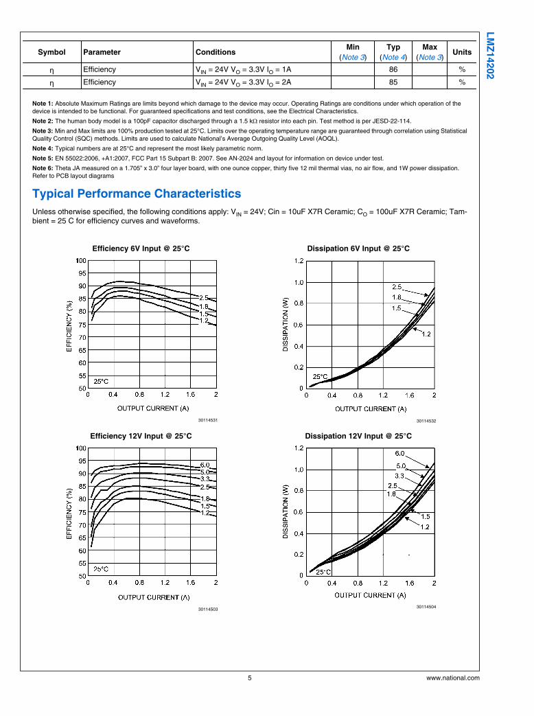
η Efficiency VIN = 24V VO = 3.3V IO = 1A 86 %
η Efficiency VIN = 24V VO = 3.3V IO = 2A 85 %
Note 1: Absolute Maximum Ratings are limits beyond which damage to the device may occur. Operating Ratings are conditions under which operation of thedevice is intended to be functional. For guaranteed specifications and test conditions, see the Electrical Characteristics.
Note 2: The human body model is a 100pF capacitor discharged through a 1.5 kΩ resistor into each pin. Test method is per JESD-22-114.
Note 3: Min and Max limits are 100% production tested at 25°C. Limits over the operating temperature range are guaranteed through correlation using StatisticalQuality Control (SQC) methods. Limits are used to calculate National’s Average Outgoing Quality Level (AOQL).
Note 4: Typical numbers are at 25°C and represent the most likely parametric norm.
Note 5: EN 55022:2006, +A1:2007, FCC Part 15 Subpart B: 2007. See AN-2024 and layout for information on device under test.
Note 6: Theta JA measured on a 1.705” x 3.0” four layer board, with one ounce copper, thirty five 12 mil thermal vias, no air flow, and 1W power dissipation.Refer to PCB layout diagrams
Typical Performance Characteristics
Unless otherwise specified, the following conditions apply: VIN = 24V; Cin = 10uF X7R Ceramic; CO = 100uF X7R Ceramic; Tam-bient = 25 C for efficiency curves and waveforms.
Efficiency 6V Input @ 25°C
30114531
Dissipation 6V Input @ 25°C
30114532
Efficiency 12V Input @ 25°C
30114503
Dissipation 12V Input @ 25°C
30114504
5 www.national.com
LM
Z14202
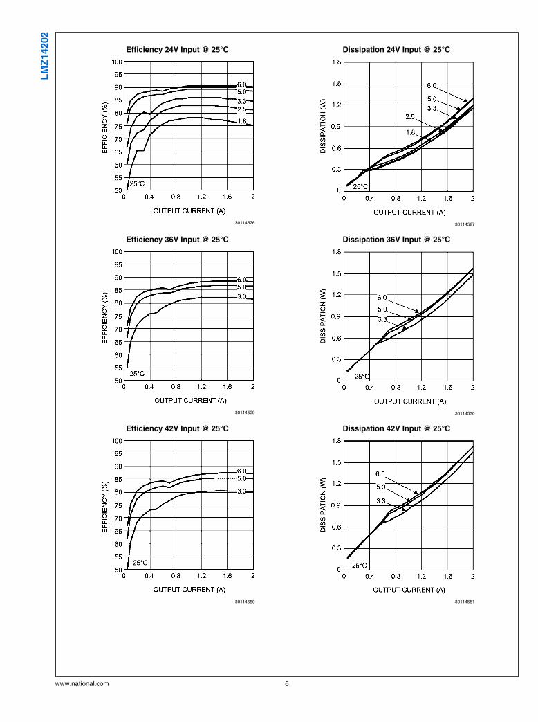
Efficiency 24V Input @ 25°C
30114526
Dissipation 24V Input @ 25°C
30114527
Efficiency 36V Input @ 25°C
30114529
Dissipation 36V Input @ 25°C
30114530
Efficiency 42V Input @ 25°C
30114550
Dissipation 42V Input @ 25°C
30114551
www.national.com 6
LM
Z14202
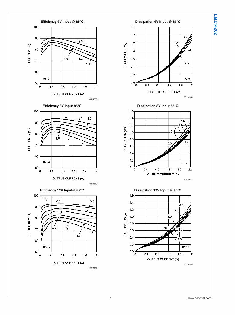
Efficiency 6V Input @ 85°C
30114533
Dissipation 6V Input @ 85°C
30114534
Efficiency 8V Input 85°C
30114540
Dissipation 8V Input 85°C
30114541
Efficiency 12V Input@ 85°C
30114542
Dissipation 12V Input @ 85°C
30114543
7 www.national.com
LM
Z14202
Efficiency 24V Input @ 85°C
30114544
Dissipation 24V Input @ 85°C
30114545
Efficiency 36V Input @ 85°C
30114546
Dissipation 36V Input @ 85°C
30114547
Efficiency 42V Input @ 85°C
30114552
Dissipation 42V Input @ 85°C
30114553
www.national.com 8
LM
Z14202
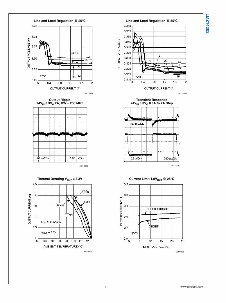
Line and Load Regulation @ 25°C
30114548
Line and Load Regulation @ 85°C
30114569
Output Ripple24VIN 3.3VO 2A, BW = 200 MHz
30114505
Transient Response24VIN 3.3VO 0.6A to 2A Step
30114506
Thermal Derating VOUT = 3.3V
30114570
Current Limit 1.8VOUT @ 25°C
30114565
9 www.national.com
LM
Z14202
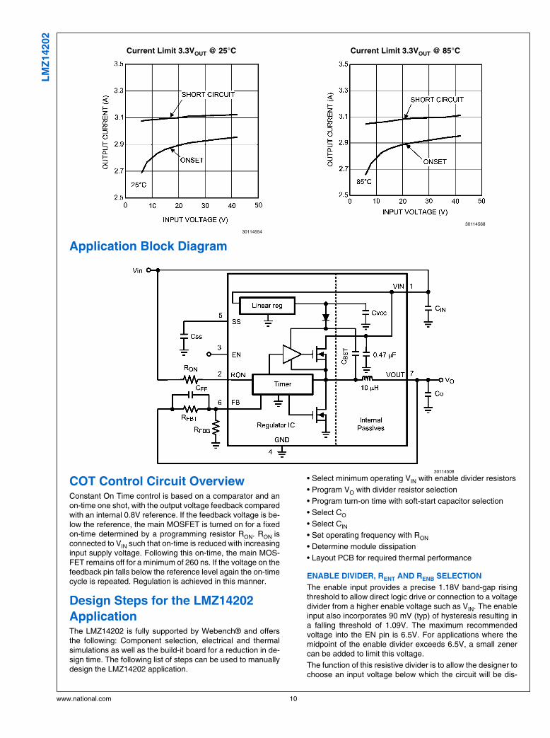
Current Limit 3.3VOUT @ 25°C
30114554
Current Limit 3.3VOUT @ 85°C
30114568
Application Block Diagram
30114508
COT Control Circuit OverviewConstant On Time control is based on a comparator and anon-time one shot, with the output voltage feedback comparedwith an internal 0.8V reference. If the feedback voltage is be-low the reference, the main MOSFET is turned on for a fixedon-time determined by a programming resistor RON. RON isconnected to VIN such that on-time is reduced with increasinginput supply voltage. Following this on-time, the main MOS-FET remains off for a minimum of 260 ns. If the voltage on thefeedback pin falls below the reference level again the on-timecycle is repeated. Regulation is achieved in this manner.
Design Steps for the LMZ14202
ApplicationThe LMZ14202 is fully supported by Webench® and offersthe following: Component selection, electrical and thermalsimulations as well as the build-it board for a reduction in de-sign time. The following list of steps can be used to manuallydesign the LMZ14202 application.
• Select minimum operating VIN with enable divider resistors
• Program VO with divider resistor selection
• Program turn-on time with soft-start capacitor selection
• Select CO
• Select CIN
• Set operating frequency with RON
• Determine module dissipation
• Layout PCB for required thermal performance
ENABLE DIVIDER, RENT AND RENB SELECTION
The enable input provides a precise 1.18V band-gap risingthreshold to allow direct logic drive or connection to a voltagedivider from a higher enable voltage such as VIN. The enableinput also incorporates 90 mV (typ) of hysteresis resulting ina falling threshold of 1.09V. The maximum recommendedvoltage into the EN pin is 6.5V. For applications where themidpoint of the enable divider exceeds 6.5V, a small zenercan be added to limit this voltage.
The function of this resistive divider is to allow the designer tochoose an input voltage below which the circuit will be dis-
www.national.com 10
LM
Z14202
abled. This implements the feature of programmable undervoltage lockout. This is often used in battery powered systemsto prevent deep discharge of the system battery. It is alsouseful in system designs for sequencing of output rails or toprevent early turn-on of the supply as the main input voltagerail rises at power-up. Applying the enable divider to the maininput rail is often done in the case of higher input voltage sys-tems such as 24V AC/DC systems where a lower boundaryof operation should be established. In the case of sequencingsupplies, the divider is connected to a rail that becomes activeearlier in the power-up cycle than the LMZ14202 output rail.The two resistors should be chosen based on the followingratio:
RENT / RENB = (VIN UVLO/ 1.18V) – 1 (1)
The LMZ14202 demonstration and evaluation boards use11.8kΩ for RENB and 68.1kΩ for RENT resulting in a rising UV-LO of 8V. This divider presents 6.25V to the EN input whenthe divider input is raised to 42V.
The EN pin is internally pulled up to VIN and can be left float-ing for always-on operation.
OUTPUT VOLTAGE SELECTION
Output voltage is determined by a divider of two resistorsconnected between VO and ground. The midpoint of the di-vider is connected to the FB input. The voltage at FB iscompared to a 0.8V internal reference. In normal operationan on-time cycle is initiated when the voltage on the FB pinfalls below 0.8V. The main MOSFET on-time cycle causes theoutput voltage to rise and the voltage at the FB to exceed0.8V. As long as the voltage at FB is above 0.8V, on-timecycles will not occur.
The regulated output voltage determined by the external di-vider resistors RFBT and RFBB is:
VO = 0.8V * (1 + RFBT / RFBB) (2)
Rearranging terms; the ratio of the feedback resistors for adesired output voltage is:
RFBT / RFBB = (VO / 0.8V) - 1 (3)
These resistors should be chosen from values in the range of1.0 kohm to 10.0 kohm.
For VO = 0.8V the FB pin can be connected to the output di-rectly so long as an output preload resistor remains that drawsmore than 20uA. Converter operation requires this minimumload to create a small inductor ripple current and maintainproper regulation when no load is present.
A feed-forward capacitor is placed in parallel with RFBT to im-prove load step transient response. Its value is usually deter-mined experimentally by load stepping between DCM andCCM conduction modes and adjusting for best transient re-sponse and minimum output ripple.
A table of values for RFBT , RFBB , CFF and RON is included inthe applications schematic.
SOFT-START CAPACITOR SELECTION
Programmable soft-start permits the regulator to slowly rampto its steady state operating point after being enabled, therebyreducing current inrush from the input supply and slowing theoutput voltage rise-time to prevent overshoot.
Upon turn-on, after all UVLO conditions have been passed,an internal 8uA current source begins charging the externalsoft-start capacitor. The soft-start time duration to reachsteady state operation is given by the formula:
tSS = VREF * CSS / Iss = 0.8V * CSS / 8uA (4)
This equation can be rearranged as follows:
CSS = tSS * 8 μA / 0.8V (5)
Use of a 0.022μF capacitor results in 2.2msec soft-start du-ration which is recommended as a minimum value.
As the soft-start input exceeds 0.8V the output of the powerstage will be in regulation. The soft-start capacitor continuescharging until it reaches approximately 3.8V on the SS pin.Voltage levels between 0.8V and 3.8V have no effect on othercircuit operation. Note that the following conditions will resetthe soft-start capacitor by discharging the SS input to groundwith an internal 200 μA current sink.
• The enable input being “pulled low”
• Thermal shutdown condition
• Over-current fault
• Internal Vcc UVLO (Approx 4V input to VIN)
CO SELECTION
None of the required CO output capacitance is contained with-in the module. At a minimum, the output capacitor must meetthe worst case minimum ripple current rating of 0.5 * ILR P-P,as calculated in equation (19) below. Beyond that, additionalcapacitance will reduce output ripple so long as the ESR islow enough to permit it. A minimum value of 10 μF is generallyrequired. Experimentation will be required if attempting to op-erate with a minimum value. Ceramic capacitors or other lowESR types are recommended. See AN-2024 for more detail.
The following equation provides a good first pass approxima-tion of CO for load transient requirements:
CO≥ISTEP*VFB*L*VIN/ (4*VO*(VIN—VO)*VOUT-TRAN)(6)
Solving:
CO≥ 2A*0.8V*10μH*24V / (4*3.3V*( 24V — 3.3V)*33mV)
≥ 43μF (7)
The LMZ14202 demonstration and evaluation boards arepopulated with a 100 uF 6.3V X5R output capacitor. Locationsfor extra output capacitors are provided. See AN-2024 for lo-cations.
CIN SELECTION
The LMZ14202 module contains an internal 0.47 µF input ce-ramic capacitor. Additional input capacitance is required ex-ternal to the module to handle the input ripple current of theapplication. This input capacitance should be located in veryclose proximity to the module. Input capacitor selection isgenerally directed to satisfy the input ripple current require-ments rather than by capacitance value. Worst case inputripple current rating is dictated by the equation:
I(CIN(RMS)) ≊ 1 /2 * IO * √ (D / 1-D) (8)
where D ≊ VO / VIN
(As a point of reference, the worst case ripple current will oc-cur when the module is presented with full load current andwhen VIN = 2 * VO).
Recommended minimum input capacitance is 10uF X7R ce-ramic with a voltage rating at least 25% higher than themaximum applied input voltage for the application. It is alsorecommended that attention be paid to the voltage and tem-perature deratings of the capacitor selected. It should benoted that ripple current rating of ceramic capacitors may bemissing from the capacitor data sheet and you may have tocontact the capacitor manufacturer for this rating.
If the system design requires a certain minimum value of inputripple voltage ΔVIN be maintained then the following equationmay be used.
CIN ≥ IO * D * (1–D) / fSW-CCM * ΔVIN(9)
11 www.national.com
LM
Z14202
If ΔVIN is 1% of VIN for a 24V input to 3.3V output applicationthis equals 240 mV and fSW = 400 kHz.
CIN≥ 2A * 3.3V/24V * (1– 3.3V/24V) / (400000 * 0.240 V)
≥ 2.5μF
Additional bulk capacitance with higher ESR may be requiredto damp any resonant effects of the input capacitance andparasitic inductance of the incoming supply lines.
RON RESISTOR SELECTION
Many designs will begin with a desired switching frequency inmind. For that purpose the following equation can be used.
fSW(CCM) ≊ VO / (1.3 * 10-10 * RON) (10)
This can be rearranged as
RON ≊ VO / (1.3 * 10 -10 * fSW(CCM) (11)
The selection of RON and fSW(CCM) must be confined by limi-tations in the on-time and off-time for the COT control section.
The on-time of the LMZ14202 timer is determined by the re-sistor RON and the input voltage VIN. It is calculated as follows:
tON = (1.3 * 10-10 * RON) / VIN (12)
The inverse relationship of tON and VIN gives a nearly constantswitching frequency as VIN is varied. RON should be selectedsuch that the on-time at maximum VIN is greater than 150 ns.The on-timer has a limiter to ensure a minimum of 150 ns fortON. This limits the maximum operating frequency, which isgoverned by the following equation:
fSW(MAX) = VO / (VIN(MAX) * 150 nsec) (13)
This equation can be used to select RON if a certain operatingfrequency is desired so long as the minimum on-time of 150ns is observed. The limit for RON can be calculated as follows:
RON ≥ VIN(MAX) * 150 nsec / (1.3 * 10 -10) (14)
If RON calculated in (11) is less than the minimum value de-termined in (14) a lower frequency should be selected. Alter-natively, VIN(MAX) can also be limited in order to keep thefrequency unchanged.
Additionally note, the minimum off-time of 260 ns limits themaximum duty ratio. Larger RON (lower FSW) should be se-lected in any application requiring large duty ratio.
Discontinuous Conduction and Continuous ConductionModes
At light load the regulator will operate in discontinuous con-duction mode (DCM). With load currents above the criticalconduction point, it will operate in continuous conductionmode (CCM). When operating in DCM the switching cyclebegins at zero amps inductor current; increases up to a peakvalue, and then recedes back to zero before the end of theoff-time. Note that during the period of time that inductor cur-rent is zero, all load current is supplied by the output capacitor.The next on-time period starts when the voltage on the at theFB pin falls below the internal reference. The switching fre-quency is lower in DCM and varies more with load current ascompared to CCM. Conversion efficiency in DCM is main-tained since conduction and switching losses are reducedwith the smaller load and lower switching frequency. Operat-ing frequency in DCM can be calculated as follows:
fSW(DCM)≊VO*(VIN-1)*10μH*1.18*1020*IO/(VIN–VO)*RON2 (15)
In CCM, current flows through the inductor through the entireswitching cycle and never falls to zero during the off-time. Theswitching frequency remains relatively constant with load cur-rent and line voltage variations. The CCM operating frequen-cy can be calculated using equation 7 above.
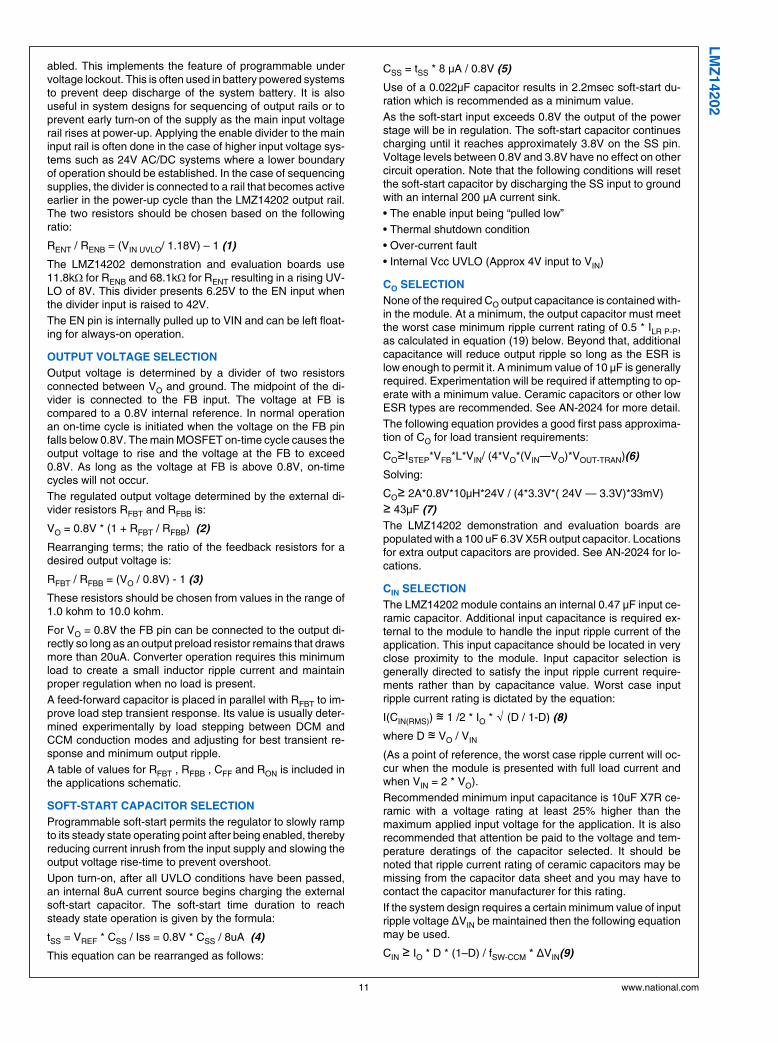
Following is a comparison pair of waveforms of the showingboth CCM (upper) and DCM operating modes.
CCM and DCM Operating ModesVIN = 24V, VO = 3.3V, IO = 2A/0.32A 2 μsec/div
30114512
The approximate formula for determining the DCM/CCMboundary is as follows:
IDCB≊VO*(VIN–VO)/(2*10 μH*fSW(CCM)*VIN) (16)
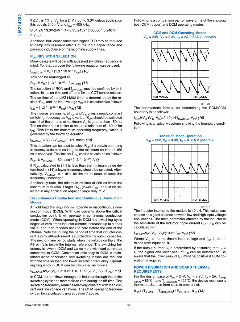
Following is a typical waveform showing the boundary condi-tion.
Transition Mode OperationVIN = 24V, VO = 3.3V, IO = 0.35A 2 μsec/div
30114514
The inductor internal to the module is 10 μH. This value waschosen as a good balance between low and high input voltageapplications. The main parameter affected by the inductor isthe amplitude of the inductor ripple current (ILR). ILR can becalculated with:
ILR P-P=VO*(VIN- VO)/(10µH*fSW*VIN) (17)
Where VIN is the maximum input voltage and fSW is deter-mined from equation 10.
If the output current IO is determined by assuming that IO =IL, the higher and lower peak of ILR can be determined. Beaware that the lower peak of ILR must be positive if CCM op-eration is required.
POWER DISSIPATION AND BOARD THERMALREQUIREMENTS
For the design case of VIN = 24V, VO = 3.3V, IO = 2A, TAMB
(MAX) = 85°C , and TJUNCTION = 125°C, the device must see athermal resistance from case to ambient of:
θCA< (TJ-MAX — TAMB(MAX)) / PIC-LOSS - θJC (18)
www.national.com 12
LM
Z14202
Given the typical thermal resistance from junction to case tobe 1.9 °C/W. Use the 85°C power dissipation curves in theTypical Performance Characteristics section to estimate thePIC-LOSS for the application being designed. In this applicationit is 1.5W.
θCA = (125 — 85) / 1.5W — 1.9) = 24.8
To reach θCA = 24.8, the PCB is required to dissipate heateffectively. With no airflow and no external heat, a good esti-mate of the required board area covered by 1 oz. copper onboth the top and bottom metal layers is:
Board Area_cm2 = 500°C x cm2/W / θJC (19)
As a result, approximately 20.2 square cm of 1 oz copper ontop and bottom layers is required for the PCB design. ThePCB copper heat sink must be connected to the exposed pad.Approximately thirty six, 10mils (254 μm) thermal vias spaced59mils (1.5 mm) apart must connect the top copper to thebottom copper. For an example of a high thermal performancePCB layout, refer to the Evaluation Board application noteAN-2024.
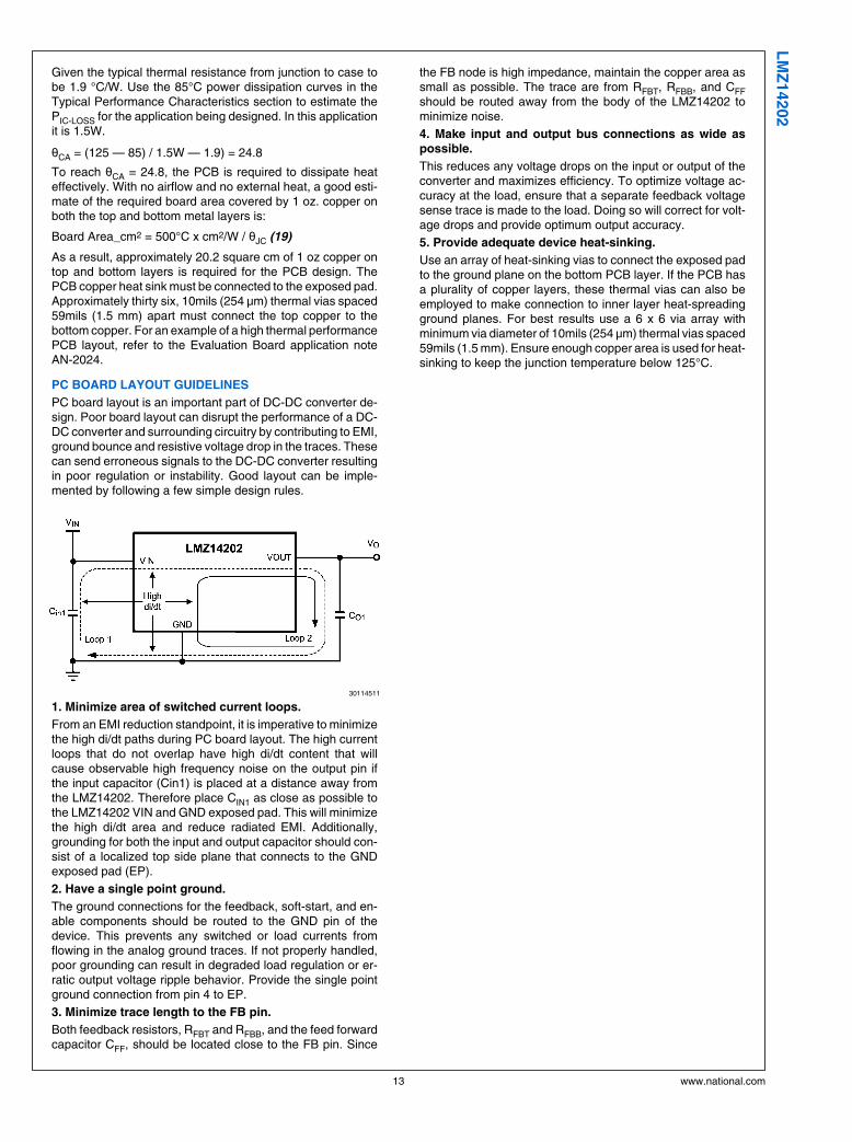
PC BOARD LAYOUT GUIDELINES
PC board layout is an important part of DC-DC converter de-sign. Poor board layout can disrupt the performance of a DC-DC converter and surrounding circuitry by contributing to EMI,ground bounce and resistive voltage drop in the traces. Thesecan send erroneous signals to the DC-DC converter resultingin poor regulation or instability. Good layout can be imple-mented by following a few simple design rules.
30114511
1. Minimize area of switched current loops.
From an EMI reduction standpoint, it is imperative to minimizethe high di/dt paths during PC board layout. The high currentloops that do not overlap have high di/dt content that willcause observable high frequency noise on the output pin ifthe input capacitor (Cin1) is placed at a distance away fromthe LMZ14202. Therefore place CIN1 as close as possible tothe LMZ14202 VIN and GND exposed pad. This will minimizethe high di/dt area and reduce radiated EMI. Additionally,grounding for both the input and output capacitor should con-sist of a localized top side plane that connects to the GNDexposed pad (EP).
2. Have a single point ground.
The ground connections for the feedback, soft-start, and en-able components should be routed to the GND pin of thedevice. This prevents any switched or load currents fromflowing in the analog ground traces. If not properly handled,poor grounding can result in degraded load regulation or er-ratic output voltage ripple behavior. Provide the single pointground connection from pin 4 to EP.
3. Minimize trace length to the FB pin.
Both feedback resistors, RFBT and RFBB, and the feed forwardcapacitor CFF, should be located close to the FB pin. Since
the FB node is high impedance, maintain the copper area assmall as possible. The trace are from RFBT, RFBB, and CFFshould be routed away from the body of the LMZ14202 tominimize noise.
4. Make input and output bus connections as wide aspossible.
This reduces any voltage drops on the input or output of theconverter and maximizes efficiency. To optimize voltage ac-curacy at the load, ensure that a separate feedback voltagesense trace is made to the load. Doing so will correct for volt-age drops and provide optimum output accuracy.
5. Provide adequate device heat-sinking.
Use an array of heat-sinking vias to connect the exposed padto the ground plane on the bottom PCB layer. If the PCB hasa plurality of copper layers, these thermal vias can also beemployed to make connection to inner layer heat-spreadingground planes. For best results use a 6 x 6 via array withminimum via diameter of 10mils (254 μm) thermal vias spaced59mils (1.5 mm). Ensure enough copper area is used for heat-sinking to keep the junction temperature below 125°C.
13 www.national.com
LM
Z14202
Additional Features
OUTPUT OVER-VOLTAGE COMPARATOR
The voltage at FB is compared to a 0.92V internal reference.If FB rises above 0.92V the on-time is immediately terminat-ed. This condition is known as over-voltage protection (OVP).It can occur if the input voltage is increased very suddenly orif the output load is decreased very suddenly. Once OVP isactivated, the top MOSFET on-times will be inhibited until thecondition clears. Additionally, the synchronous MOSFET willremain on until inductor current falls to zero.
CURRENT LIMIT
Current limit detection is carried out during the off-time bymonitoring the current in the synchronous MOSFET. Refer-ring to the Functional Block Diagram, when the top MOSFETis turned off, the inductor current flows through the load, thePGND pin and the internal synchronous MOSFET. If this cur-rent exceeds 2.6 A (typical) the current limit comparator dis-ables the start of the next on-time period. The next switchingcycle will occur only if the FB input is less than 0.8V and theinductor current has decreased below 2.6 A. Inductor currentis monitored during the period of time the synchronous MOS-FET is conducting. So long as inductor current exceeds 2.6A,further on-time intervals for the top MOSFET will not occur.Switching frequency is lower during current limit due to thelonger off-time. It should also be noted that current limit isdependent on both duty cycle and temperature as illustratedin the graphs in the typical performance section.
THERMAL PROTECTION
The junction temperature of the LMZ14202 should not be al-lowed to exceed its maximum ratings. Thermal protection isimplemented by an internal Thermal Shutdown circuit whichactivates at 165 °C (typ) causing the device to enter a lowpower standby state. In this state the main MOSFET remainsoff causing VO to fall, and additionally the CSS capacitor isdischarged to ground. Thermal protection helps preventcatastrophic failures for accidental device overheating. Whenthe junction temperature falls back below 145 °C (typ Hyst =20 °C) the SS pin is released, VO rises smoothly, and normaloperation resumes.
Applications requiring maximum output current especiallythose at high input voltage may require application deratingat elevated temperatures.
ZERO COIL CURRENT DETECTION
The current of the lower (synchronous) MOSFET is monitoredby a zero coil current detection circuit which inhibits the syn-chronous MOSFET when its current reaches zero until thenext on-time. This circuit enables the DCM operating mode,which improves efficiency at light loads.
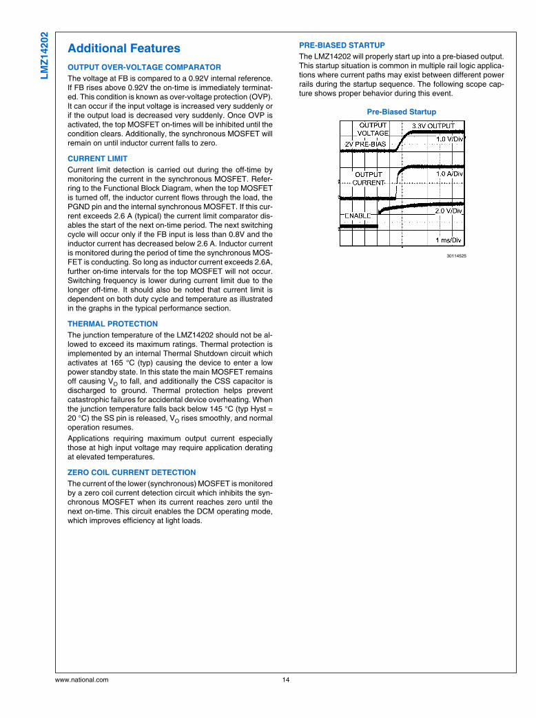
PRE-BIASED STARTUP
The LMZ14202 will properly start up into a pre-biased output.This startup situation is common in multiple rail logic applica-tions where current paths may exist between different powerrails during the startup sequence. The following scope cap-ture shows proper behavior during this event.
Pre-Biased Startup
30114525
www.national.com 14
LM
Z14202
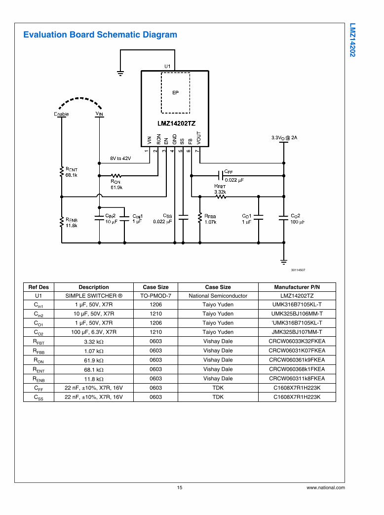
Evaluation Board Schematic Diagram
30114507
Ref Des Description Case Size Case Size Manufacturer P/N
U1 SIMPLE SWITCHER ® TO-PMOD-7 National Semiconductor LMZ14202TZ
Cin1 1 µF, 50V, X7R 1206 Taiyo Yuden UMK316B7105KL-T
Cin2 10 µF, 50V, X7R 1210 Taiyo Yuden UMK325BJ106MM-T
CO1 1 µF, 50V, X7R 1206 Taiyo Yuden 'UMK316B7105KL-T
CO2 100 µF, 6.3V, X7R 1210 Taiyo Yuden JMK325BJ107MM-T
RFBT 3.32 kΩ 0603 Vishay Dale CRCW06033K32FKEA
RFBB 1.07 kΩ 0603 Vishay Dale CRCW06031K07FKEA
RON 61.9 kΩ 0603 Vishay Dale CRCW060361k9FKEA
RENT 68.1 kΩ 0603 Vishay Dale CRCW060368k1FKEA
RENB 11.8 kΩ 0603 Vishay Dale CRCW060311k8FKEA
CFF 22 nF, ±10%, X7R, 16V 0603 TDK C1608X7R1H223K
CSS 22 nF, ±10%, X7R, 16V 0603 TDK C1608X7R1H223K
15 www.national.com
LM
Z14202
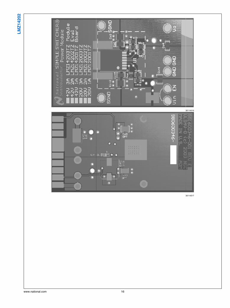
30114516
30114517
www.national.com 16
LM
Z14202
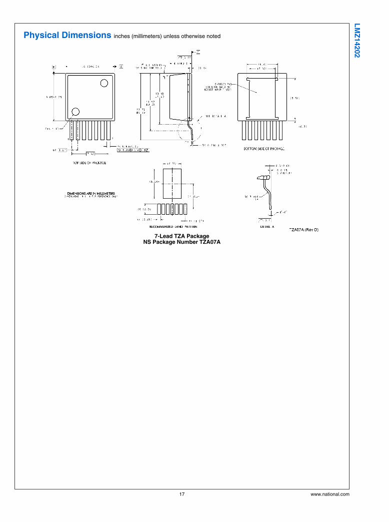
Physical Dimensions inches (millimeters) unless otherwise noted
7-Lead TZA PackageNS Package Number TZA07A
17 www.national.com
LM
Z14202
NotesL
MZ
14202 2
A S
IMP
LE
SW
ITC
HE
R®
Po
wer
Mo
du
le w
ith
42V
Maxim
um
In
pu
t V
olt
ag
e
For more National Semiconductor product information and proven design tools, visit the following Web sites at:
www.national.com
Products Design Support
Amplifiers www.national.com/amplifiers WEBENCH® Tools www.national.com/webench
Audio www.national.com/audio App Notes www.national.com/appnotes
Clock and Timing www.national.com/timing Reference Designs www.national.com/refdesigns
Data Converters www.national.com/adc Samples www.national.com/samples
Interface www.national.com/interface Eval Boards www.national.com/evalboards
LVDS www.national.com/lvds Packaging www.national.com/packaging
Power Management www.national.com/power Green Compliance www.national.com/quality/green
Switching Regulators www.national.com/switchers Distributors www.national.com/contacts
LDOs www.national.com/ldo Quality and Reliability www.national.com/quality
LED Lighting www.national.com/led Feedback/Support www.national.com/feedback
Voltage References www.national.com/vref Design Made Easy www.national.com/easy
PowerWise® Solutions www.national.com/powerwise Applications & Markets www.national.com/solutions
Serial Digital Interface (SDI) www.national.com/sdi Mil/Aero www.national.com/milaero
Temperature Sensors www.national.com/tempsensors SolarMagic™ www.national.com/solarmagic
PLL/VCO www.national.com/wireless PowerWise® DesignUniversity
www.national.com/training
THE CONTENTS OF THIS DOCUMENT ARE PROVIDED IN CONNECTION WITH NATIONAL SEMICONDUCTOR CORPORATION(“NATIONAL”) PRODUCTS. NATIONAL MAKES NO REPRESENTATIONS OR WARRANTIES WITH RESPECT TO THE ACCURACYOR COMPLETENESS OF THE CONTENTS OF THIS PUBLICATION AND RESERVES THE RIGHT TO MAKE CHANGES TOSPECIFICATIONS AND PRODUCT DESCRIPTIONS AT ANY TIME WITHOUT NOTICE. NO LICENSE, WHETHER EXPRESS,IMPLIED, ARISING BY ESTOPPEL OR OTHERWISE, TO ANY INTELLECTUAL PROPERTY RIGHTS IS GRANTED BY THISDOCUMENT.
TESTING AND OTHER QUALITY CONTROLS ARE USED TO THE EXTENT NATIONAL DEEMS NECESSARY TO SUPPORTNATIONAL’S PRODUCT WARRANTY. EXCEPT WHERE MANDATED BY GOVERNMENT REQUIREMENTS, TESTING OF ALLPARAMETERS OF EACH PRODUCT IS NOT NECESSARILY PERFORMED. NATIONAL ASSUMES NO LIABILITY FORAPPLICATIONS ASSISTANCE OR BUYER PRODUCT DESIGN. BUYERS ARE RESPONSIBLE FOR THEIR PRODUCTS ANDAPPLICATIONS USING NATIONAL COMPONENTS. PRIOR TO USING OR DISTRIBUTING ANY PRODUCTS THAT INCLUDENATIONAL COMPONENTS, BUYERS SHOULD PROVIDE ADEQUATE DESIGN, TESTING AND OPERATING SAFEGUARDS.
EXCEPT AS PROVIDED IN NATIONAL’S TERMS AND CONDITIONS OF SALE FOR SUCH PRODUCTS, NATIONAL ASSUMES NOLIABILITY WHATSOEVER, AND NATIONAL DISCLAIMS ANY EXPRESS OR IMPLIED WARRANTY RELATING TO THE SALEAND/OR USE OF NATIONAL PRODUCTS INCLUDING LIABILITY OR WARRANTIES RELATING TO FITNESS FOR A PARTICULARPURPOSE, MERCHANTABILITY, OR INFRINGEMENT OF ANY PATENT, COPYRIGHT OR OTHER INTELLECTUAL PROPERTYRIGHT.
LIFE SUPPORT POLICY
NATIONAL’S PRODUCTS ARE NOT AUTHORIZED FOR USE AS CRITICAL COMPONENTS IN LIFE SUPPORT DEVICES ORSYSTEMS WITHOUT THE EXPRESS PRIOR WRITTEN APPROVAL OF THE CHIEF EXECUTIVE OFFICER AND GENERALCOUNSEL OF NATIONAL SEMICONDUCTOR CORPORATION. As used herein:
Life support devices or systems are devices which (a) are intended for surgical implant into the body, or (b) support or sustain life andwhose failure to perform when properly used in accordance with instructions for use provided in the labeling can be reasonably expectedto result in a significant injury to the user. A critical component is any component in a life support device or system whose failure to performcan be reasonably expected to cause the failure of the life support device or system or to affect its safety or effectiveness.
National Semiconductor and the National Semiconductor logo are registered trademarks of National Semiconductor Corporation. All otherbrand or product names may be trademarks or registered trademarks of their respective holders.
Copyright© 2011 National Semiconductor Corporation
For the most current product information visit us at www.national.com
National SemiconductorAmericas TechnicalSupport CenterEmail: [email protected]: 1-800-272-9959
National Semiconductor EuropeTechnical Support CenterEmail: [email protected]
National Semiconductor AsiaPacific Technical Support CenterEmail: [email protected]
National Semiconductor JapanTechnical Support CenterEmail: [email protected]
www.national.com

IMPORTANT NOTICE
Texas Instruments Incorporated and its subsidiaries (TI) reserve the right to make corrections, modifications, enhancements, improvements,and other changes to its products and services at any time and to discontinue any product or service without notice. Customers shouldobtain the latest relevant information before placing orders and should verify that such information is current and complete. All products aresold subject to TI’s terms and conditions of sale supplied at the time of order acknowledgment.
TI warrants performance of its hardware products to the specifications applicable at the time of sale in accordance with TI’s standardwarranty. Testing and other quality control techniques are used to the extent TI deems necessary to support this warranty. Except wheremandated by government requirements, testing of all parameters of each product is not necessarily performed.
TI assumes no liability for applications assistance or customer product design. Customers are responsible for their products andapplications using TI components. To minimize the risks associated with customer products and applications, customers should provideadequate design and operating safeguards.
TI does not warrant or represent that any license, either express or implied, is granted under any TI patent right, copyright, mask work right,or other TI intellectual property right relating to any combination, machine, or process in which TI products or services are used. Informationpublished by TI regarding third-party products or services does not constitute a license from TI to use such products or services or awarranty or endorsement thereof. Use of such information may require a license from a third party under the patents or other intellectualproperty of the third party, or a license from TI under the patents or other intellectual property of TI.
Reproduction of TI information in TI data books or data sheets is permissible only if reproduction is without alteration and is accompaniedby all associated warranties, conditions, limitations, and notices. Reproduction of this information with alteration is an unfair and deceptivebusiness practice. TI is not responsible or liable for such altered documentation. Information of third parties may be subject to additionalrestrictions.
Resale of TI products or services with statements different from or beyond the parameters stated by TI for that product or service voids allexpress and any implied warranties for the associated TI product or service and is an unfair and deceptive business practice. TI is notresponsible or liable for any such statements.
TI products are not authorized for use in safety-critical applications (such as life support) where a failure of the TI product would reasonablybe expected to cause severe personal injury or death, unless officers of the parties have executed an agreement specifically governingsuch use. Buyers represent that they have all necessary expertise in the safety and regulatory ramifications of their applications, andacknowledge and agree that they are solely responsible for all legal, regulatory and safety-related requirements concerning their productsand any use of TI products in such safety-critical applications, notwithstanding any applications-related information or support that may beprovided by TI. Further, Buyers must fully indemnify TI and its representatives against any damages arising out of the use of TI products insuch safety-critical applications.
TI products are neither designed nor intended for use in military/aerospace applications or environments unless the TI products arespecifically designated by TI as military-grade or "enhanced plastic." Only products designated by TI as military-grade meet militaryspecifications. Buyers acknowledge and agree that any such use of TI products which TI has not designated as military-grade is solely atthe Buyer's risk, and that they are solely responsible for compliance with all legal and regulatory requirements in connection with such use.
TI products are neither designed nor intended for use in automotive applications or environments unless the specific TI products aredesignated by TI as compliant with ISO/TS 16949 requirements. Buyers acknowledge and agree that, if they use any non-designatedproducts in automotive applications, TI will not be responsible for any failure to meet such requirements.
Following are URLs where you can obtain information on other Texas Instruments products and application solutions:
Products Applications
Audio www.ti.com/audio Communications and Telecom www.ti.com/communications
Amplifiers amplifier.ti.com Computers and Peripherals www.ti.com/computers
Data Converters dataconverter.ti.com Consumer Electronics www.ti.com/consumer-apps
DLP® Products www.dlp.com Energy and Lighting www.ti.com/energy
DSP dsp.ti.com Industrial www.ti.com/industrial
Clocks and Timers www.ti.com/clocks Medical www.ti.com/medical
Interface interface.ti.com Security www.ti.com/security
Logic logic.ti.com Space, Avionics and Defense www.ti.com/space-avionics-defense
Power Mgmt power.ti.com Transportation and Automotive www.ti.com/automotive
Microcontrollers microcontroller.ti.com Video and Imaging www.ti.com/video
RFID www.ti-rfid.com
OMAP Mobile Processors www.ti.com/omap
Wireless Connectivity www.ti.com/wirelessconnectivity
TI E2E Community Home Page e2e.ti.com
Mailing Address: Texas Instruments, Post Office Box 655303, Dallas, Texas 75265Copyright © 2011, Texas Instruments Incorporated