LMD18201 3A, 55V H-Bridge (Rev. D) - TI.com · LMD18201 SNVS092D – APRIL 1998– REVISED APRIL...
17
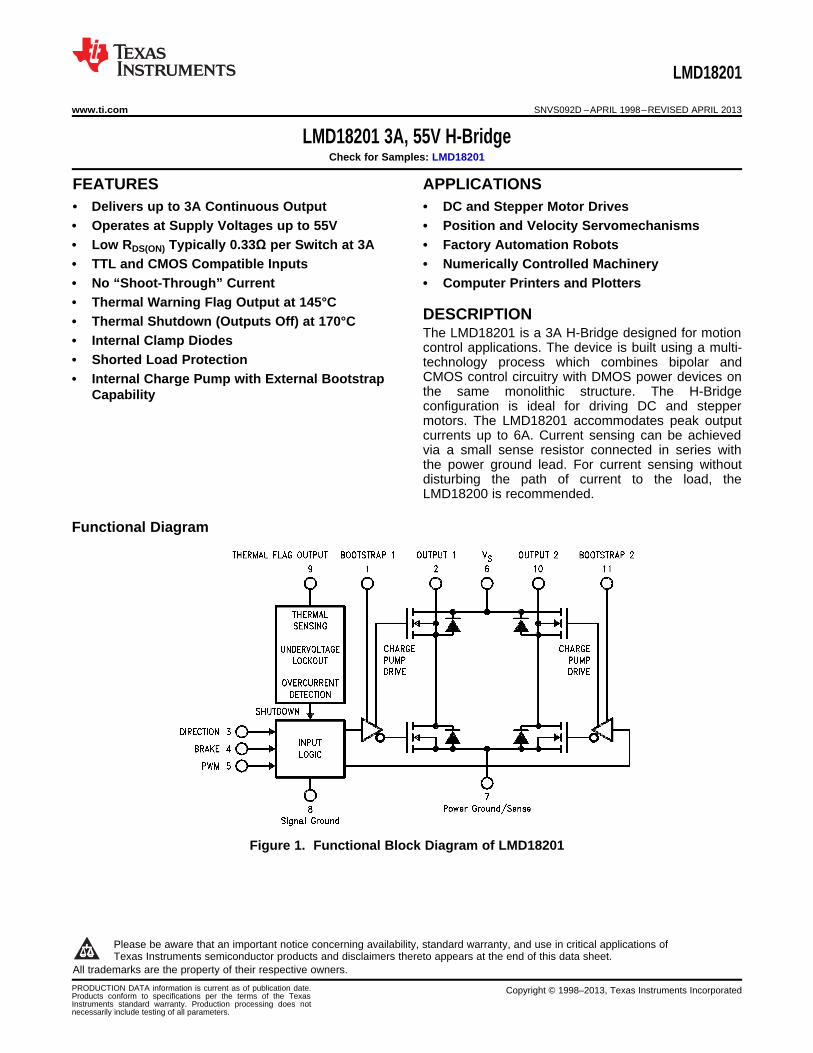
LMD18201 www.ti.com SNVS092D – APRIL 1998 – REVISED APRIL 2013 LMD18201 3A, 55V H-Bridge Check for Samples: LMD18201 1FEATURES APPLICATIONS 2• Delivers up to 3A Continuous Output • DC and Stepper Motor Drives • Operates at Supply Voltages up to 55V • Position and Velocity Servomechanisms • Low R DS(ON) Typically 0.33Ω per Switch at 3A • Factory Automation Robots • TTL and CMOS Compatible Inputs • Numerically Controlled Machinery • No “Shoot-Through” Current • Computer Printers and Plotters • Thermal Warning Flag Output at 145°C DESCRIPTION • Thermal Shutdown (Outputs Off) at 170°C The LMD18201 is a 3A H-Bridge designed for motion • Internal Clamp Diodes control applications. The device is built using a multi- • Shorted Load Protection technology process which combines bipolar and CMOS control circuitry with DMOS power devices on • Internal Charge Pump with External Bootstrap the same monolithic structure. The H-Bridge Capability configuration is ideal for driving DC and stepper motors. The LMD18201 accommodates peak output currents up to 6A. Current sensing can be achieved via a small sense resistor connected in series with the power ground lead. For current sensing without disturbing the path of current to the load, the LMD18200 is recommended. Functional Diagram Figure 1. Functional Block Diagram of LMD18201 1 Please be aware that an important notice concerning availability, standard warranty, and use in critical applications of Texas Instruments semiconductor products and disclaimers thereto appears at the end of this data sheet. 2All trademarks are the property of their respective owners. PRODUCTION DATA information is current as of publication date. Copyright © 1998–2013, Texas Instruments Incorporated Products conform to specifications per the terms of the Texas Instruments standard warranty. Production processing does not necessarily include testing of all parameters.
-
Upload
truongkhanh -
Category
Documents
-
view
215 -
download
0
Transcript of LMD18201 3A, 55V H-Bridge (Rev. D) - TI.com · LMD18201 SNVS092D – APRIL 1998– REVISED APRIL...
LMD18201
www.ti.com SNVS092D –APRIL 1998–REVISED APRIL 2013
LMD18201 3A, 55V H-BridgeCheck for Samples: LMD18201
1FEATURES APPLICATIONS2• Delivers up to 3A Continuous Output • DC and Stepper Motor Drives• Operates at Supply Voltages up to 55V • Position and Velocity Servomechanisms• Low RDS(ON) Typically 0.33Ω per Switch at 3A • Factory Automation Robots• TTL and CMOS Compatible Inputs • Numerically Controlled Machinery• No “Shoot-Through” Current • Computer Printers and Plotters• Thermal Warning Flag Output at 145°C
DESCRIPTION• Thermal Shutdown (Outputs Off) at 170°CThe LMD18201 is a 3A H-Bridge designed for motion• Internal Clamp Diodes control applications. The device is built using a multi-
• Shorted Load Protection technology process which combines bipolar andCMOS control circuitry with DMOS power devices on• Internal Charge Pump with External Bootstrapthe same monolithic structure. The H-BridgeCapabilityconfiguration is ideal for driving DC and steppermotors. The LMD18201 accommodates peak outputcurrents up to 6A. Current sensing can be achievedvia a small sense resistor connected in series withthe power ground lead. For current sensing withoutdisturbing the path of current to the load, theLMD18200 is recommended.
Functional Diagram
Figure 1. Functional Block Diagram of LMD18201
1
Please be aware that an important notice concerning availability, standard warranty, and use in critical applications ofTexas Instruments semiconductor products and disclaimers thereto appears at the end of this data sheet.
2All trademarks are the property of their respective owners.
PRODUCTION DATA information is current as of publication date. Copyright © 1998–2013, Texas Instruments IncorporatedProducts conform to specifications per the terms of the TexasInstruments standard warranty. Production processing does notnecessarily include testing of all parameters.
LMD18201
SNVS092D –APRIL 1998–REVISED APRIL 2013 www.ti.com
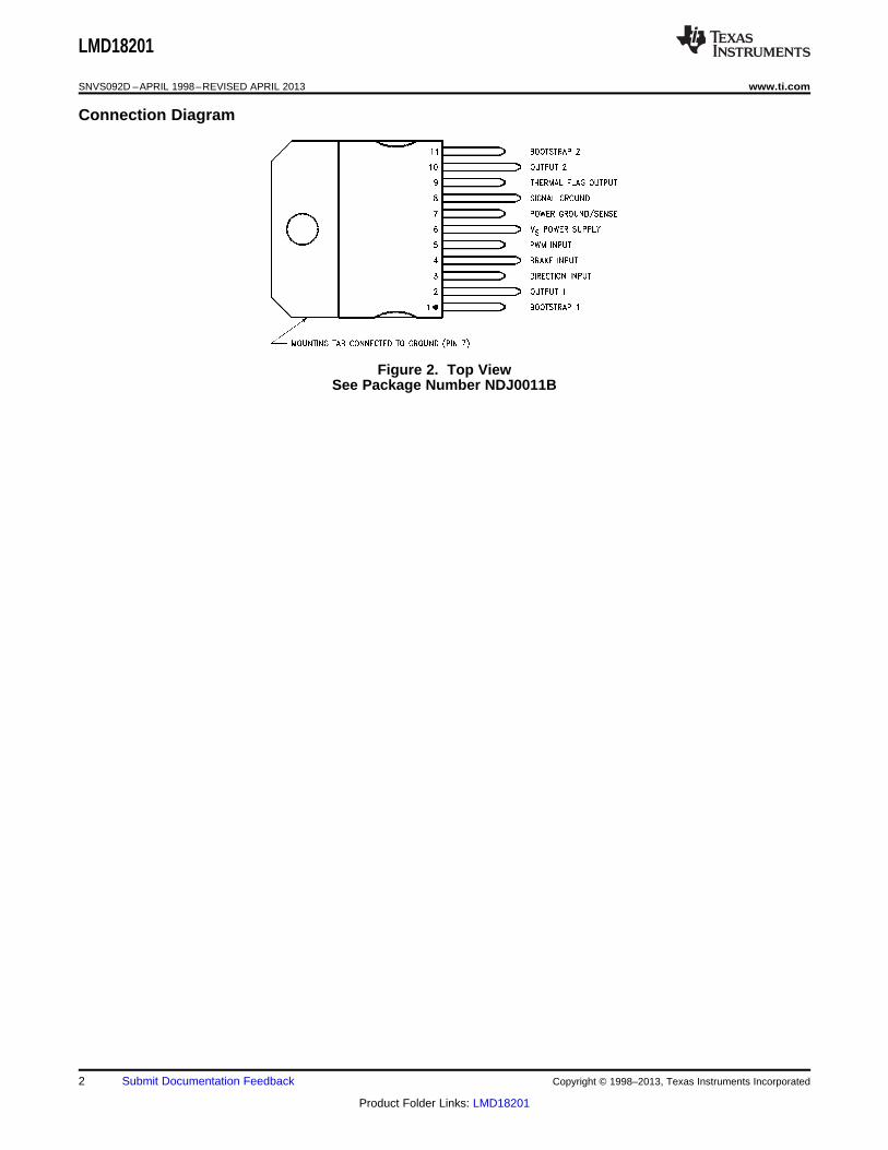
Connection Diagram
Figure 2. Top ViewSee Package Number NDJ0011B
2 Submit Documentation Feedback Copyright © 1998–2013, Texas Instruments Incorporated
Product Folder Links: LMD18201
LMD18201
www.ti.com SNVS092D –APRIL 1998–REVISED APRIL 2013
These devices have limited built-in ESD protection. The leads should be shorted together or the device placed in conductive foamduring storage or handling to prevent electrostatic damage to the MOS gates.
Absolute Maximum Ratings (1) (2)
Total Supply Voltage (VS, Pin 6) 60V
Voltage at Pins 3, 4, 5 and 9 12V
Voltage at Bootstrap Pins (Pins 1 and 11) VOUT + 16V
Peak Output Current (200 ms) 6A
Continuous Output Current (3) 3A
Power Dissipation (4) 25W
Sense Voltage (Pin 7 to Pin 8) +0.5V to −1.0V
Power Dissipation (TA = 25°C, Free Air) 3W
Junction Temperature, TJ(max) 150°C
ESD Susceptibility (5) 1500V
Storage Temperature, TSTG −40°C to +150°C
Lead Temperature (Soldering, 10 sec.) 300°C
(1) Absolute Maximum Ratings indicate limits beyond which damage to the device may occur. DC and AC electrical specifications do notapply when operating the device beyond its rated operating conditions.
(2) If Military/Aerospace specified devices are required, please contact the Texas Instruments Sales Office/Distributors for availability andspecifications.
(3) See Application Information for details regarding current limiting.(4) The maximum power dissipation must be derated at elevated temperatures and is a function of TJ(max), θJA, and TA. The maximum
allowable power dissipation at any temperature is PD(max) = (TJ(max) − TA)/θJA, or the number given in the Absolute Ratings, whichever islower. The typical thermal resistance from junction to case (θJC) is 1.0°C/W and from junction to ambient (θJA) is 30°C/W. For ensuredoperation TJ(max) = 125°C.
(5) Human-body model, 100 pF discharged through a 1.5 kΩ resistor. Except Bootstrap pins (pins 1 and 11) which are protected to 1000Vof ESD.
Operating Ratings (1)
Junction Temperature, TJ −40°C to +125°C
VS Supply Voltage +12V to +55V
(1) Absolute Maximum Ratings indicate limits beyond which damage to the device may occur. DC and AC electrical specifications do notapply when operating the device beyond its rated operating conditions.
Electrical Characteristics (1)
The following specifications apply for VS = 42V, unless otherwise specified. Boldface limits apply over the entire operatingtemperature range, −40°C ≤ TJ ≤ +125°C, all other limits are for TA = TJ = 25°C.
Symbol Parameter Conditions Typ Limit Units
RDS(ON) Switch ON Resistance Output Current = 3A (2) 0.33 0.40/0.6 Ω (max)
RDS(ON) Switch ON Resistance Output Current = 6A (2) 0.38 0.45/0.6 Ω (max)
VCLAMP Clamp Diode Forward Drop Clamp Current = 3A (2) 1.2 1.5 V (max)
VIL Logic Low Input Voltage Pins 3, 4, 5 −0.1 V (min)
0.8 V (max)
IIL Logic Low Input Current VIN = −0.1V, Pins = 3, 4, 5 −10 μA (max)
VIH Logic High Input Voltage Pins 3, 4, 5 2 V (min)
12 V (max)
IIL Logic High Input Current VIN = 12V, Pins = 3, 4, 5 10 μA (max)
Undervoltage Lockout Outputs Turn OFF 9 V (min)
11 V (max)
TJW Warning Flag Temperature Pin 9 ≤ 0.8V, IL = 2 mA 145 °C
VF(ON) Flag Output Saturation Voltage TJ = TJW, IL = 2 mA 0.15 V
(1) All limits are 100% production tested at 25°C. Temperature extreme limits are ensured via correlation using accepted SQC (StatisticalQuality Control) methods. All limits are used to calculate AOQL, (Average Outgoing Quality Level).
(2) Output currents are pulsed (tW < 2 ms, Duty Cycle < 5%).
Copyright © 1998–2013, Texas Instruments Incorporated Submit Documentation Feedback 3
Product Folder Links: LMD18201
LMD18201
SNVS092D –APRIL 1998–REVISED APRIL 2013 www.ti.com
Electrical Characteristics(1) (continued)The following specifications apply for VS = 42V, unless otherwise specified. Boldface limits apply over the entire operatingtemperature range, −40°C ≤ TJ ≤ +125°C, all other limits are for TA = TJ = 25°C.
Symbol Parameter Conditions Typ Limit Units
IF(OFF) Flag Output Leakage VF = 12V 0.2 10 μA (max)
TJSD Shutdown Temperature Outputs Turn OFF 170 °C
IS Quiescent Supply Current All Logic Inputs Low 13 25 mA (max)
tD(ON) Output Turn-On Delay Time Sourcing Outputs, IOUT = 3A 300 ns
Sinking Outputs, IOUT = 3A 300 ns
tON Output Turn-On Switching Time Bootstrap Capacitor = 10 nF
Sourcing Outputs, IOUT = 3A 100 ns
Sinking Outputs, IOUT = 3A 80 ns
tD(OFF) Output Turn-Off Delay Times Sourcing Outputs, IOUT = 3A 200 ns
Sinking Outputs, IOUT = 3A 200 ns
tOFF Output Turn-Off Switching Times Bootstrap Capacitor = 10 nF
Sourcing Outputs, IOUT = 3A 75 ns
Sinking Outputs, IOUT = 3A 70 ns
tPW Minimum Input Pulse Width Pins 3, 4 and 5 1 μs
tCPR Charge Pump Rise Time No Bootstrap Capacitor 20 μs
4 Submit Documentation Feedback Copyright © 1998–2013, Texas Instruments Incorporated
Product Folder Links: LMD18201
LMD18201
www.ti.com SNVS092D –APRIL 1998–REVISED APRIL 2013
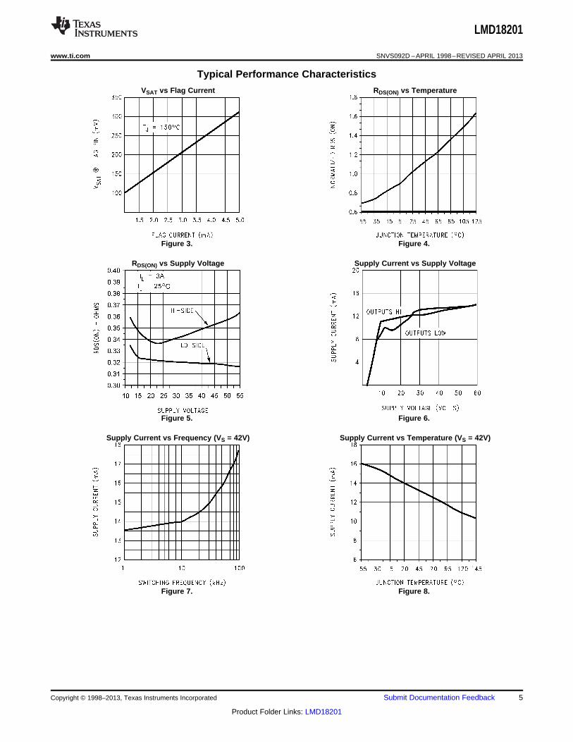
Typical Performance Characteristics
VSAT vs Flag Current RDS(ON) vs Temperature
Figure 3. Figure 4.
RDS(ON) vs Supply Voltage Supply Current vs Supply Voltage
Figure 5. Figure 6.
Supply Current vs Frequency (VS = 42V) Supply Current vs Temperature (VS = 42V)
Figure 7. Figure 8.
Copyright © 1998–2013, Texas Instruments Incorporated Submit Documentation Feedback 5
Product Folder Links: LMD18201
LMD18201
SNVS092D –APRIL 1998–REVISED APRIL 2013 www.ti.com
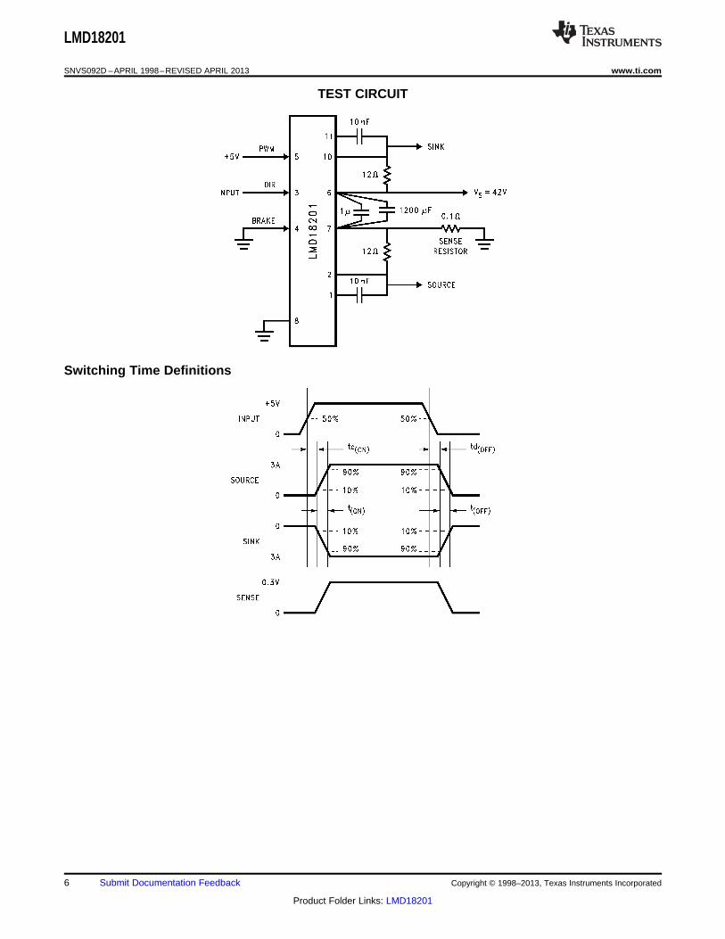
TEST CIRCUIT
Switching Time Definitions
6 Submit Documentation Feedback Copyright © 1998–2013, Texas Instruments Incorporated
Product Folder Links: LMD18201
LMD18201
www.ti.com SNVS092D –APRIL 1998–REVISED APRIL 2013
Pinout Descriptions
(See Test Circuit)
Pin 1, BOOTSTRAP 1 Input: Bootstrap capacitor pin for half H-Bridge number 1. The recommended capacitor(10 nF) is connected between pins 1 and 2.
Pin 2, OUTPUT 1: Half H-Bridge number 1 output.
Pin 3, DIRECTION Input: See Logic Truth Table. This input controls the direction of current flow betweenOUTPUT 1 and OUTPUT 2 (pins 2 and 10) and, therefore, the direction of rotation of a motor load.
Pin 4, BRAKE Input: See Logic Truth Table. This input is used to brake a motor by effectively shorting itsterminals. When braking is desired, this input is taken to a logic high level and it is also necessary to apply logichigh to PWM input, pin 5. The drivers that short the motor are determined by the logic level at the DIRECTIONinput (Pin 3): with Pin 3 logic high, both current sourcing output transistors are ON; with Pin 3 logic low, bothcurrent sinking output transistors are ON. All output transistors can be turned OFF by applying a logic high to Pin4 and a logic low to PWM input Pin 5; in this case only a small bias current (approximately −1.5 mA) exists ateach output pin.
Pin 5, PWM Input: See Logic Truth Table. How this input (and DIRECTION input, Pin 3) is used is determinedby the format of the PWM Signal.
Pin 6, VS Power Supply
Pin 7, POWER GROUND/SENSE Connection: This pin is the ground return for the power DMOS transistors ofthe H-Bridge. The current through the H-Bridge can be sensed by adding a small, 0.1Ω, sense resistor from thispin to the power supply ground.
Pin 8, SIGNAL GROUND: This is the ground return for the internal logic circuitry used to control the PWMswitching of the H-Bridge.
Pin 9, THERMAL FLAG Output: This pin provides the thermal warning flag output signal. Pin 9 becomes active-low at 145°C (junction temperature). However the chip will not shut itself down until 170°C is reached at thejunction.
Pin 10, OUTPUT 2: Half H-Bridge number 2 output.
Pin 11, BOOTSTRAP 2 Input: Bootstrap capacitor pin for half H-Bridge number 2. The recommended capacitor(10 nF) is connected between pins 10 and 11.
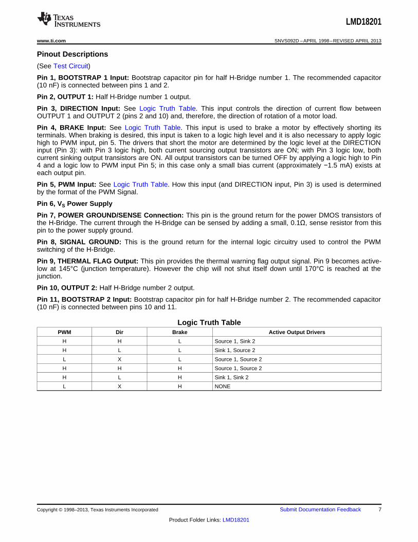
Logic Truth TablePWM Dir Brake Active Output Drivers
H H L Source 1, Sink 2
H L L Sink 1, Source 2
L X L Source 1, Source 2
H H H Source 1, Source 2
H L H Sink 1, Sink 2
L X H NONE
Copyright © 1998–2013, Texas Instruments Incorporated Submit Documentation Feedback 7
Product Folder Links: LMD18201
LMD18201
SNVS092D –APRIL 1998–REVISED APRIL 2013 www.ti.com
APPLICATION INFORMATION
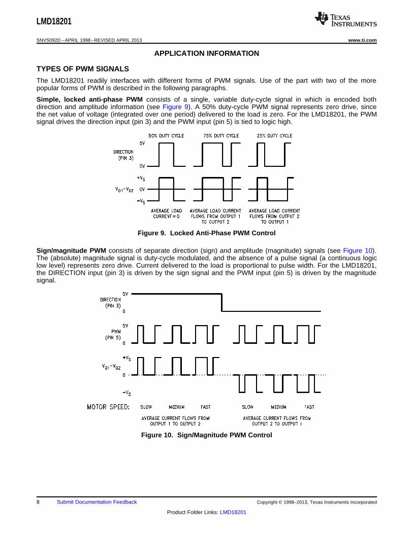
TYPES OF PWM SIGNALS
The LMD18201 readily interfaces with different forms of PWM signals. Use of the part with two of the morepopular forms of PWM is described in the following paragraphs.
Simple, locked anti-phase PWM consists of a single, variable duty-cycle signal in which is encoded bothdirection and amplitude information (see Figure 9). A 50% duty-cycle PWM signal represents zero drive, sincethe net value of voltage (integrated over one period) delivered to the load is zero. For the LMD18201, the PWMsignal drives the direction input (pin 3) and the PWM input (pin 5) is tied to logic high.
Figure 9. Locked Anti-Phase PWM Control
Sign/magnitude PWM consists of separate direction (sign) and amplitude (magnitude) signals (see Figure 10).The (absolute) magnitude signal is duty-cycle modulated, and the absence of a pulse signal (a continuous logiclow level) represents zero drive. Current delivered to the load is proportional to pulse width. For the LMD18201,the DIRECTION input (pin 3) is driven by the sign signal and the PWM input (pin 5) is driven by the magnitudesignal.
Figure 10. Sign/Magnitude PWM Control
8 Submit Documentation Feedback Copyright © 1998–2013, Texas Instruments Incorporated
Product Folder Links: LMD18201
LMD18201
www.ti.com SNVS092D –APRIL 1998–REVISED APRIL 2013
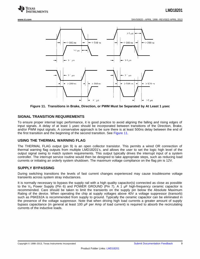
Figure 11. Transitions in Brake, Direction, or PWM Must be Separated by At Least 1 μsec
SIGNAL TRANSITION REQUIREMENTS
To ensure proper internal logic performance, it is good practice to avoid aligning the falling and rising edges ofinput signals. A delay of at least 1 µsec should be incorporated between transitions of the Direction, Brake,and/or PWM input signals. A conservative approach is be sure there is at least 500ns delay between the end ofthe first transition and the beginning of the second transition. See Figure 11.
USING THE THERMAL WARNING FLAG
The THERMAL FLAG output (pin 9) is an open collector transistor. This permits a wired OR connection ofthermal warning flag outputs from multiple LMD18201's, and allows the user to set the logic high level of theoutput signal swing to match system requirements. This output typically drives the interrupt input of a systemcontroller. The interrupt service routine would then be designed to take appropriate steps, such as reducing loadcurrents or initiating an orderly system shutdown. The maximum voltage compliance on the flag pin is 12V.
SUPPLY BYPASSING
During switching transitions the levels of fast current changes experienced may cause troublesome voltagetransients across system stray inductances.
It is normally necessary to bypass the supply rail with a high quality capacitor(s) connected as close as possibleto the VS Power Supply (Pin 6) and POWER GROUND (Pin 7). A 1 μF high-frequency ceramic capacitor isrecommended. Care should be taken to limit the transients on the supply pin below the Absolute MaximumRating of the device. When operating the chip at supply voltages above 40V a voltage suppressor (transorb)such as P6KE62A is recommended from supply to ground. Typically the ceramic capacitor can be eliminated inthe presence of the voltage suppressor. Note that when driving high load currents a greater amount of supplybypass capacitance (in general at least 100 μF per Amp of load current) is required to absorb the recirculatingcurrents of the inductive loads.
Copyright © 1998–2013, Texas Instruments Incorporated Submit Documentation Feedback 9
Product Folder Links: LMD18201
LMD18201
SNVS092D –APRIL 1998–REVISED APRIL 2013 www.ti.com
CURRENT LIMITING
Current limiting protection circuitry has been incorporated into the design of the LMD18201. With any powerdevice it is important to consider the effects of the substantial surge currents through the device that may occuras a result of shorted loads. The protection circuitry monitors the current through the upper transistors and shutsoff the power device as quickly as possible in the event of an overload condition (the threshold is set toapproximately 10A). In a typical motor driving application the most common overload faults are caused byshorted motor windings and locked rotors. Under these conditions the inductance of the motor (as well as anyseries inductance in the VCC supply line) serves to reduce the magnitude of a current surge to a safe level for theLMD18201. Once the device is shut down, the control circuitry will periodically try to turn the power device backon. This feature allows the immediate return to normal operation once the fault condition has been removed.While the fault remains however, the device will cycle in and out of thermal shutdown. This can create voltagetransients on the VCC supply line and therefore proper supply bypassing techniques are required.
The most severe condition for any power device is a direct, hard-wired (“screwdriver”) long term short from anoutput to ground. This condition can generate a surge of current through the power device on the order of 15Amps and require the die and package to dissipate up to 500W of power for the short time required for theprotection circuitry to shut off the power device. This energy can be destructive, particularly at higher operatingvoltages (>30V) so some precautions are in order. Proper heat sink design is essential and it is normallynecessary to heat sink the VCC supply pin (pin 6) with 1 square inch of copper on the PC board.
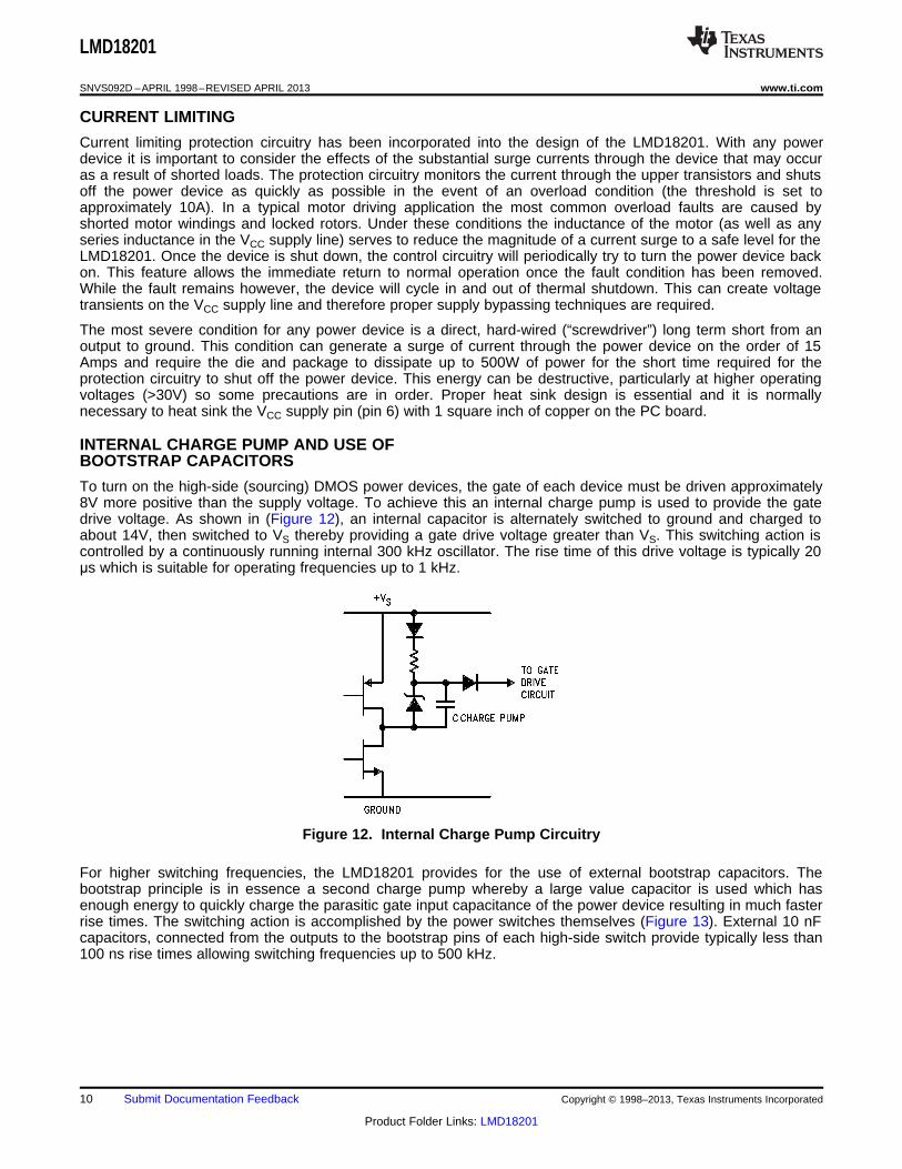
INTERNAL CHARGE PUMP AND USE OFBOOTSTRAP CAPACITORS
To turn on the high-side (sourcing) DMOS power devices, the gate of each device must be driven approximately8V more positive than the supply voltage. To achieve this an internal charge pump is used to provide the gatedrive voltage. As shown in (Figure 12), an internal capacitor is alternately switched to ground and charged toabout 14V, then switched to VS thereby providing a gate drive voltage greater than VS. This switching action iscontrolled by a continuously running internal 300 kHz oscillator. The rise time of this drive voltage is typically 20μs which is suitable for operating frequencies up to 1 kHz.
Figure 12. Internal Charge Pump Circuitry
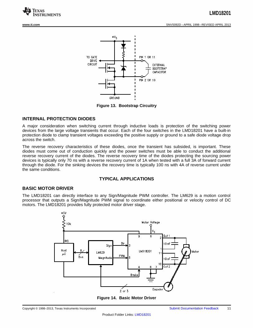
For higher switching frequencies, the LMD18201 provides for the use of external bootstrap capacitors. Thebootstrap principle is in essence a second charge pump whereby a large value capacitor is used which hasenough energy to quickly charge the parasitic gate input capacitance of the power device resulting in much fasterrise times. The switching action is accomplished by the power switches themselves (Figure 13). External 10 nFcapacitors, connected from the outputs to the bootstrap pins of each high-side switch provide typically less than100 ns rise times allowing switching frequencies up to 500 kHz.
10 Submit Documentation Feedback Copyright © 1998–2013, Texas Instruments Incorporated
Product Folder Links: LMD18201
LMD18201
www.ti.com SNVS092D –APRIL 1998–REVISED APRIL 2013
Figure 13. Bootstrap Circuitry
INTERNAL PROTECTION DIODES
A major consideration when switching current through inductive loads is protection of the switching powerdevices from the large voltage transients that occur. Each of the four switches in the LMD18201 have a built-inprotection diode to clamp transient voltages exceeding the positive supply or ground to a safe diode voltage dropacross the switch.
The reverse recovery characteristics of these diodes, once the transient has subsided, is important. Thesediodes must come out of conduction quickly and the power switches must be able to conduct the additionalreverse recovery current of the diodes. The reverse recovery time of the diodes protecting the sourcing powerdevices is typically only 70 ns with a reverse recovery current of 1A when tested with a full 3A of forward currentthrough the diode. For the sinking devices the recovery time is typically 100 ns with 4A of reverse current underthe same conditions.
TYPICAL APPLICATIONS
BASIC MOTOR DRIVER
The LMD18201 can directly interface to any Sign/Magnitude PWM controller. The LM629 is a motion controlprocessor that outputs a Sign/Magnitude PWM signal to coordinate either positional or velocity control of DCmotors. The LMD18201 provides fully protected motor driver stage.
Figure 14. Basic Motor Driver
Copyright © 1998–2013, Texas Instruments Incorporated Submit Documentation Feedback 11
Product Folder Links: LMD18201
LMD18201
SNVS092D –APRIL 1998–REVISED APRIL 2013 www.ti.com
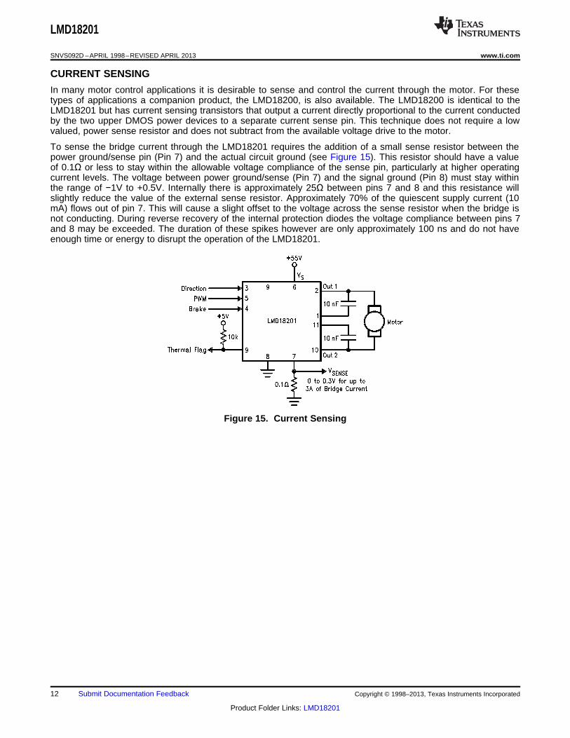
CURRENT SENSING
In many motor control applications it is desirable to sense and control the current through the motor. For thesetypes of applications a companion product, the LMD18200, is also available. The LMD18200 is identical to theLMD18201 but has current sensing transistors that output a current directly proportional to the current conductedby the two upper DMOS power devices to a separate current sense pin. This technique does not require a lowvalued, power sense resistor and does not subtract from the available voltage drive to the motor.
To sense the bridge current through the LMD18201 requires the addition of a small sense resistor between thepower ground/sense pin (Pin 7) and the actual circuit ground (see Figure 15). This resistor should have a valueof 0.1Ω or less to stay within the allowable voltage compliance of the sense pin, particularly at higher operatingcurrent levels. The voltage between power ground/sense (Pin 7) and the signal ground (Pin 8) must stay withinthe range of −1V to +0.5V. Internally there is approximately 25Ω between pins 7 and 8 and this resistance willslightly reduce the value of the external sense resistor. Approximately 70% of the quiescent supply current (10mA) flows out of pin 7. This will cause a slight offset to the voltage across the sense resistor when the bridge isnot conducting. During reverse recovery of the internal protection diodes the voltage compliance between pins 7and 8 may be exceeded. The duration of these spikes however are only approximately 100 ns and do not haveenough time or energy to disrupt the operation of the LMD18201.
Figure 15. Current Sensing
12 Submit Documentation Feedback Copyright © 1998–2013, Texas Instruments Incorporated
Product Folder Links: LMD18201
LMD18201
www.ti.com SNVS092D –APRIL 1998–REVISED APRIL 2013
REVISION HISTORY
Changes from Revision C (April 2013) to Revision D Page
• Changed layout of National Data Sheet to TI format .......................................................................................................... 12
Copyright © 1998–2013, Texas Instruments Incorporated Submit Documentation Feedback 13
Product Folder Links: LMD18201
PACKAGE OPTION ADDENDUM
www.ti.com 1-Nov-2013
Addendum-Page 1
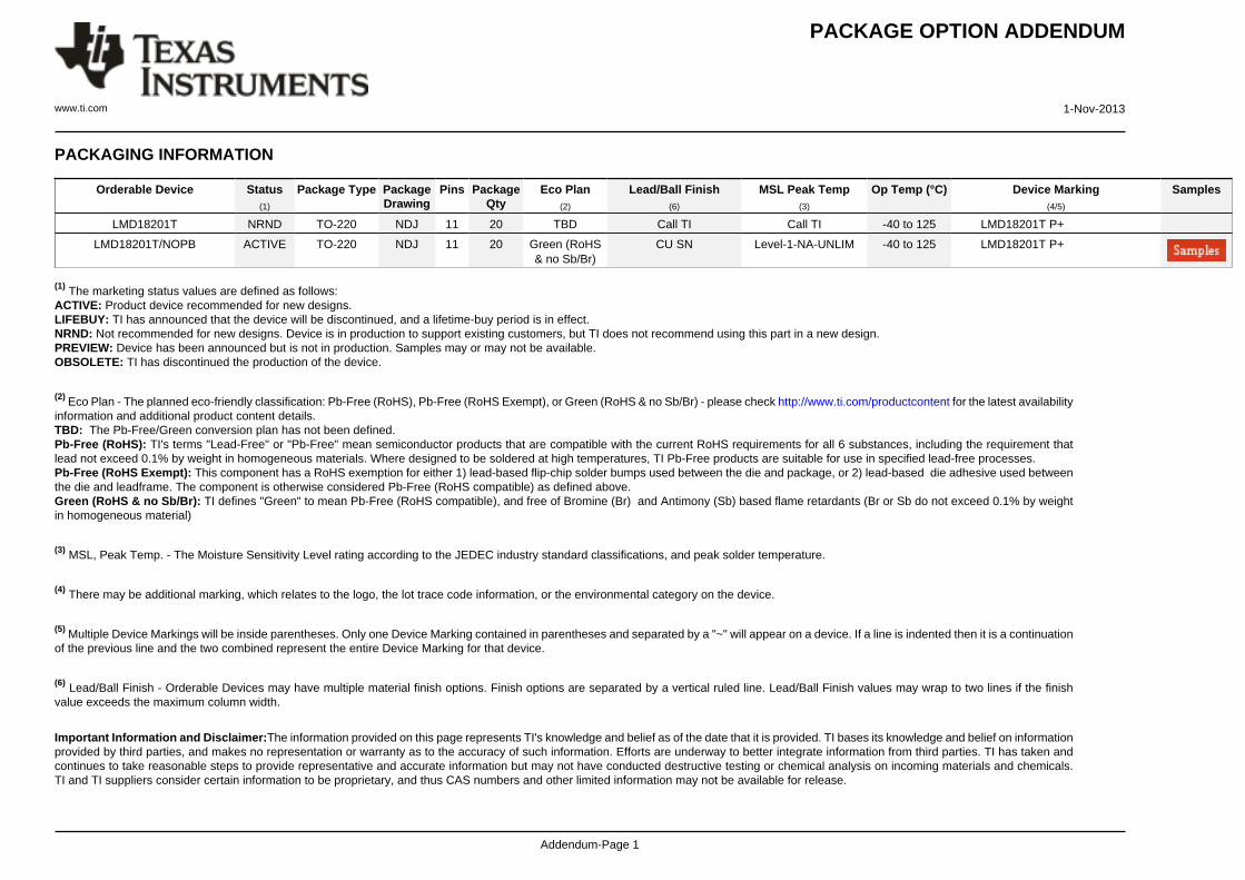
PACKAGING INFORMATION
Orderable Device Status(1)
Package Type PackageDrawing
Pins PackageQty
Eco Plan(2)
Lead/Ball Finish(6)
MSL Peak Temp(3)
Op Temp (°C) Device Marking(4/5)
Samples
LMD18201T NRND TO-220 NDJ 11 20 TBD Call TI Call TI -40 to 125 LMD18201T P+
LMD18201T/NOPB ACTIVE TO-220 NDJ 11 20 Green (RoHS& no Sb/Br)
CU SN Level-1-NA-UNLIM -40 to 125 LMD18201T P+
(1) The marketing status values are defined as follows:ACTIVE: Product device recommended for new designs.LIFEBUY: TI has announced that the device will be discontinued, and a lifetime-buy period is in effect.NRND: Not recommended for new designs. Device is in production to support existing customers, but TI does not recommend using this part in a new design.PREVIEW: Device has been announced but is not in production. Samples may or may not be available.OBSOLETE: TI has discontinued the production of the device.
(2) Eco Plan - The planned eco-friendly classification: Pb-Free (RoHS), Pb-Free (RoHS Exempt), or Green (RoHS & no Sb/Br) - please check http://www.ti.com/productcontent for the latest availabilityinformation and additional product content details.TBD: The Pb-Free/Green conversion plan has not been defined.Pb-Free (RoHS): TI's terms "Lead-Free" or "Pb-Free" mean semiconductor products that are compatible with the current RoHS requirements for all 6 substances, including the requirement thatlead not exceed 0.1% by weight in homogeneous materials. Where designed to be soldered at high temperatures, TI Pb-Free products are suitable for use in specified lead-free processes.Pb-Free (RoHS Exempt): This component has a RoHS exemption for either 1) lead-based flip-chip solder bumps used between the die and package, or 2) lead-based die adhesive used betweenthe die and leadframe. The component is otherwise considered Pb-Free (RoHS compatible) as defined above.Green (RoHS & no Sb/Br): TI defines "Green" to mean Pb-Free (RoHS compatible), and free of Bromine (Br) and Antimony (Sb) based flame retardants (Br or Sb do not exceed 0.1% by weightin homogeneous material)
(3) MSL, Peak Temp. - The Moisture Sensitivity Level rating according to the JEDEC industry standard classifications, and peak solder temperature.
(4) There may be additional marking, which relates to the logo, the lot trace code information, or the environmental category on the device.
(5) Multiple Device Markings will be inside parentheses. Only one Device Marking contained in parentheses and separated by a "~" will appear on a device. If a line is indented then it is a continuationof the previous line and the two combined represent the entire Device Marking for that device.
(6) Lead/Ball Finish - Orderable Devices may have multiple material finish options. Finish options are separated by a vertical ruled line. Lead/Ball Finish values may wrap to two lines if the finishvalue exceeds the maximum column width.
Important Information and Disclaimer:The information provided on this page represents TI's knowledge and belief as of the date that it is provided. TI bases its knowledge and belief on informationprovided by third parties, and makes no representation or warranty as to the accuracy of such information. Efforts are underway to better integrate information from third parties. TI has taken andcontinues to take reasonable steps to provide representative and accurate information but may not have conducted destructive testing or chemical analysis on incoming materials and chemicals.TI and TI suppliers consider certain information to be proprietary, and thus CAS numbers and other limited information may not be available for release.
PACKAGE OPTION ADDENDUM
www.ti.com 1-Nov-2013
Addendum-Page 2
In no event shall TI's liability arising out of such information exceed the total purchase price of the TI part(s) at issue in this document sold by TI to Customer on an annual basis.
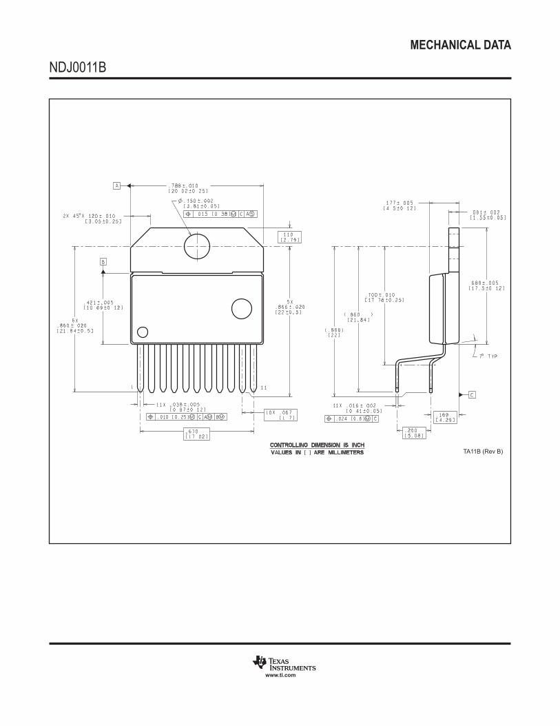
MECHANICAL DATA
NDJ0011B
www.ti.com
TA11B (Rev B)
IMPORTANT NOTICE
Texas Instruments Incorporated and its subsidiaries (TI) reserve the right to make corrections, enhancements, improvements and otherchanges to its semiconductor products and services per JESD46, latest issue, and to discontinue any product or service per JESD48, latestissue. Buyers should obtain the latest relevant information before placing orders and should verify that such information is current andcomplete. All semiconductor products (also referred to herein as “components”) are sold subject to TI’s terms and conditions of salesupplied at the time of order acknowledgment.
TI warrants performance of its components to the specifications applicable at the time of sale, in accordance with the warranty in TI’s termsand conditions of sale of semiconductor products. Testing and other quality control techniques are used to the extent TI deems necessaryto support this warranty. Except where mandated by applicable law, testing of all parameters of each component is not necessarilyperformed.
TI assumes no liability for applications assistance or the design of Buyers’ products. Buyers are responsible for their products andapplications using TI components. To minimize the risks associated with Buyers’ products and applications, Buyers should provideadequate design and operating safeguards.
TI does not warrant or represent that any license, either express or implied, is granted under any patent right, copyright, mask work right, orother intellectual property right relating to any combination, machine, or process in which TI components or services are used. Informationpublished by TI regarding third-party products or services does not constitute a license to use such products or services or a warranty orendorsement thereof. Use of such information may require a license from a third party under the patents or other intellectual property of thethird party, or a license from TI under the patents or other intellectual property of TI.
Reproduction of significant portions of TI information in TI data books or data sheets is permissible only if reproduction is without alterationand is accompanied by all associated warranties, conditions, limitations, and notices. TI is not responsible or liable for such altereddocumentation. Information of third parties may be subject to additional restrictions.
Resale of TI components or services with statements different from or beyond the parameters stated by TI for that component or servicevoids all express and any implied warranties for the associated TI component or service and is an unfair and deceptive business practice.TI is not responsible or liable for any such statements.
Buyer acknowledges and agrees that it is solely responsible for compliance with all legal, regulatory and safety-related requirementsconcerning its products, and any use of TI components in its applications, notwithstanding any applications-related information or supportthat may be provided by TI. Buyer represents and agrees that it has all the necessary expertise to create and implement safeguards whichanticipate dangerous consequences of failures, monitor failures and their consequences, lessen the likelihood of failures that might causeharm and take appropriate remedial actions. Buyer will fully indemnify TI and its representatives against any damages arising out of the useof any TI components in safety-critical applications.
In some cases, TI components may be promoted specifically to facilitate safety-related applications. With such components, TI’s goal is tohelp enable customers to design and create their own end-product solutions that meet applicable functional safety standards andrequirements. Nonetheless, such components are subject to these terms.
No TI components are authorized for use in FDA Class III (or similar life-critical medical equipment) unless authorized officers of the partieshave executed a special agreement specifically governing such use.
Only those TI components which TI has specifically designated as military grade or “enhanced plastic” are designed and intended for use inmilitary/aerospace applications or environments. Buyer acknowledges and agrees that any military or aerospace use of TI componentswhich have not been so designated is solely at the Buyer's risk, and that Buyer is solely responsible for compliance with all legal andregulatory requirements in connection with such use.
TI has specifically designated certain components as meeting ISO/TS16949 requirements, mainly for automotive use. In any case of use ofnon-designated products, TI will not be responsible for any failure to meet ISO/TS16949.
Products Applications
Audio www.ti.com/audio Automotive and Transportation www.ti.com/automotive
Amplifiers amplifier.ti.com Communications and Telecom www.ti.com/communications
Data Converters dataconverter.ti.com Computers and Peripherals www.ti.com/computers
DLP® Products www.dlp.com Consumer Electronics www.ti.com/consumer-apps
DSP dsp.ti.com Energy and Lighting www.ti.com/energy
Clocks and Timers www.ti.com/clocks Industrial www.ti.com/industrial
Interface interface.ti.com Medical www.ti.com/medical
Logic logic.ti.com Security www.ti.com/security
Power Mgmt power.ti.com Space, Avionics and Defense www.ti.com/space-avionics-defense
Microcontrollers microcontroller.ti.com Video and Imaging www.ti.com/video
RFID www.ti-rfid.com
OMAP Applications Processors www.ti.com/omap TI E2E Community e2e.ti.com
Wireless Connectivity www.ti.com/wirelessconnectivity
Mailing Address: Texas Instruments, Post Office Box 655303, Dallas, Texas 75265Copyright © 2013, Texas Instruments Incorporated


![CURVATURE AND RADIUS OF CURVATURE - …theengineeringmaths.com/wp-content/uploads/2017/09/... · · 2017-09-08CURVATURE AND RADIUS OF CURVATURE ... 3a [–2 cos + ] ... Example](https://static.fdocument.org/doc/165x107/5abbe2677f8b9ab1118d81dc/curvature-and-radius-of-curvature-and-radius-of-curvature-3a-2-cos.jpg)