LM96000 Hardware Monitor with Integrated Fan … · LM96000 SNAS234C – APRIL 2004– REVISED...
40
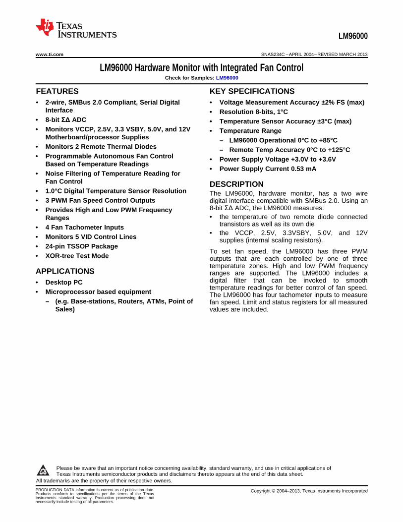
LM96000 www.ti.com SNAS234C – APRIL 2004 – REVISED MARCH 2013 LM96000 Hardware Monitor with Integrated Fan Control Check for Samples: LM96000 1FEATURES KEY SPECIFICATIONS 2• 2-wire, SMBus 2.0 Compliant, Serial Digital • Voltage Measurement Accuracy ±2% FS (max) Interface • Resolution 8-bits, 1°C • 8-bit ΣΔ ADC • Temperature Sensor Accuracy ±3°C (max) • Monitors VCCP, 2.5V, 3.3 VSBY, 5.0V, and 12V • Temperature Range Motherboard/processor Supplies – LM96000 Operational 0°C to +85°C • Monitors 2 Remote Thermal Diodes – Remote Temp Accuracy 0°C to +125°C • Programmable Autonomous Fan Control • Power Supply Voltage +3.0V to +3.6V Based on Temperature Readings • Power Supply Current 0.53 mA • Noise Filtering of Temperature Reading for Fan Control DESCRIPTION • 1.0°C Digital Temperature Sensor Resolution The LM96000, hardware monitor, has a two wire • 3 PWM Fan Speed Control Outputs digital interface compatible with SMBus 2.0. Using an 8-bit ΣΔ ADC, the LM96000 measures: • Provides High and Low PWM Frequency • the temperature of two remote diode connected Ranges transistors as well as its own die • 4 Fan Tachometer Inputs • the VCCP, 2.5V, 3.3VSBY, 5.0V, and 12V • Monitors 5 VID Control Lines supplies (internal scaling resistors). • 24-pin TSSOP Package To set fan speed, the LM96000 has three PWM • XOR-tree Test Mode outputs that are each controlled by one of three temperature zones. High and low PWM frequency APPLICATIONS ranges are supported. The LM96000 includes a digital filter that can be invoked to smooth • Desktop PC temperature readings for better control of fan speed. • Microprocessor based equipment The LM96000 has four tachometer inputs to measure – (e.g. Base-stations, Routers, ATMs, Point of fan speed. Limit and status registers for all measured Sales) values are included. 1 Please be aware that an important notice concerning availability, standard warranty, and use in critical applications of Texas Instruments semiconductor products and disclaimers thereto appears at the end of this data sheet. 2All trademarks are the property of their respective owners. PRODUCTION DATA information is current as of publication date. Copyright © 2004–2013, Texas Instruments Incorporated Products conform to specifications per the terms of the Texas Instruments standard warranty. Production processing does not necessarily include testing of all parameters.
Transcript of LM96000 Hardware Monitor with Integrated Fan … · LM96000 SNAS234C – APRIL 2004– REVISED...
LM96000
www.ti.com SNAS234C –APRIL 2004–REVISED MARCH 2013
LM96000 Hardware Monitor with Integrated Fan ControlCheck for Samples: LM96000
1FEATURES KEY SPECIFICATIONS2• 2-wire, SMBus 2.0 Compliant, Serial Digital • Voltage Measurement Accuracy ±2% FS (max)
Interface • Resolution 8-bits, 1°C• 8-bit ΣΔ ADC • Temperature Sensor Accuracy ±3°C (max)• Monitors VCCP, 2.5V, 3.3 VSBY, 5.0V, and 12V • Temperature Range
Motherboard/processor Supplies – LM96000 Operational 0°C to +85°C• Monitors 2 Remote Thermal Diodes – Remote Temp Accuracy 0°C to +125°C• Programmable Autonomous Fan Control • Power Supply Voltage +3.0V to +3.6V
Based on Temperature Readings• Power Supply Current 0.53 mA
• Noise Filtering of Temperature Reading forFan Control DESCRIPTION
• 1.0°C Digital Temperature Sensor Resolution The LM96000, hardware monitor, has a two wire• 3 PWM Fan Speed Control Outputs digital interface compatible with SMBus 2.0. Using an
8-bit ΣΔ ADC, the LM96000 measures:• Provides High and Low PWM Frequency• the temperature of two remote diode connectedRanges
transistors as well as its own die• 4 Fan Tachometer Inputs• the VCCP, 2.5V, 3.3VSBY, 5.0V, and 12V
• Monitors 5 VID Control Lines supplies (internal scaling resistors).• 24-pin TSSOP Package
To set fan speed, the LM96000 has three PWM• XOR-tree Test Mode outputs that are each controlled by one of three
temperature zones. High and low PWM frequencyAPPLICATIONS ranges are supported. The LM96000 includes a
digital filter that can be invoked to smooth• Desktop PCtemperature readings for better control of fan speed.
• Microprocessor based equipment The LM96000 has four tachometer inputs to measure– (e.g. Base-stations, Routers, ATMs, Point of fan speed. Limit and status registers for all measured
Sales) values are included.
1
Please be aware that an important notice concerning availability, standard warranty, and use in critical applications ofTexas Instruments semiconductor products and disclaimers thereto appears at the end of this data sheet.
2All trademarks are the property of their respective owners.
PRODUCTION DATA information is current as of publication date. Copyright © 2004–2013, Texas Instruments IncorporatedProducts conform to specifications per the terms of the TexasInstruments standard warranty. Production processing does notnecessarily include testing of all parameters.
LM96000
11
1
2
3
4
5
6
7
8
10
12
9
24
23
14
13
22
21
20
19
18
17
16
15
TACH4/AddSel
PWM1/xTESTOUT
VCCP_IN
2.5V
12V
5V
VID4
REMOTE1+
REMOTE1-
REMOTE2-
PWM3/AddEnable
REMOTE2+
SMBDAT
SMBCLK
TACH1
TACH2
GND
3.3V
VID0
VID1
VID2
VID3
TACH3
PWM2
SERIAL BUS
INTERFACE
VOLTAGE, FAN SPEED,
TEMPERATURE, AND
LIMIT VALUE REGISTERS
LIMIT COMPARATORS
STATUS REGISTERS
CONFIGURATION
REGISTERS
FAN TMIN/TRANGE/
HYST REGISTERS
FAN SPEED CONFIG.
REGISTERS
FAN PWM CONTROL
& PWM VALUE
REGISTERS
8-bit 6' ADC
BANDGAP
REFERENCE
INPUT
ATTENUATORS,
EXTERNAL DIODE
SIGNAL
CONDITIONING,
AND
ANALOG
MULTIPLEXER
VID0-4
REGISTER
ADDRESS
POINTER
REGISTER
STEPPING AND
DEVICE ID
REGISTERS
FAN SPEED
COUNTER
INTERNAL
TEMP
SENSOR
3.3SBY
5VIN
12VIN
2.5VIN
VCCP_IN
REMOTE1+REMOTE1-
REMOTE2-
REMOTE2+
SMBDAT
SMBCLK
PWM1
PWM2
PWM3/
Address
Enable
FAN CHARACTERISTICS
VID0VID1VID2VID3VID4
TACH1
TACH2
TACH3TACH4/
Address Select
SPIKE SMOOTHING
VDD
LM96000
SNAS234C –APRIL 2004–REVISED MARCH 2013 www.ti.com
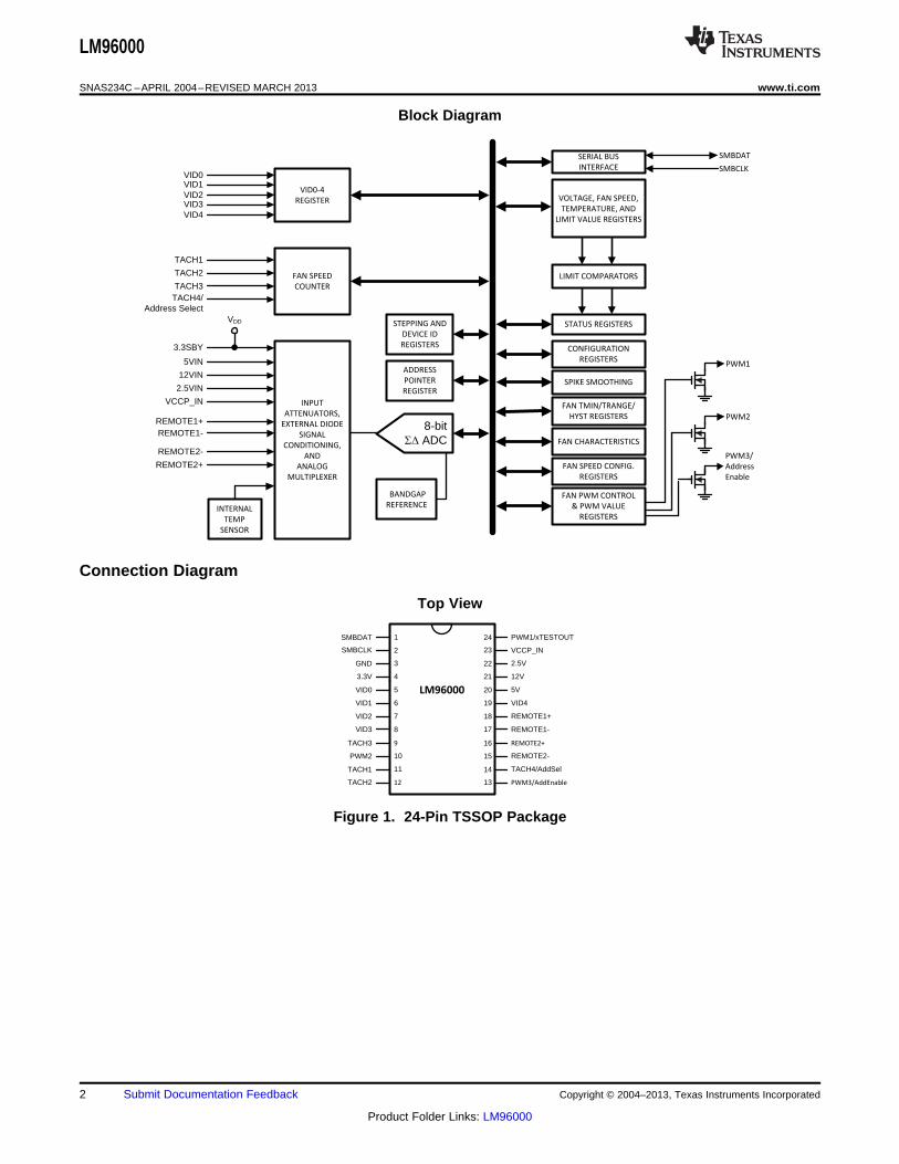
Block Diagram
Connection Diagram
Top View
Figure 1. 24-Pin TSSOP Package
2 Submit Documentation Feedback Copyright © 2004–2013, Texas Instruments Incorporated
Product Folder Links: LM96000
LM96000
www.ti.com SNAS234C –APRIL 2004–REVISED MARCH 2013
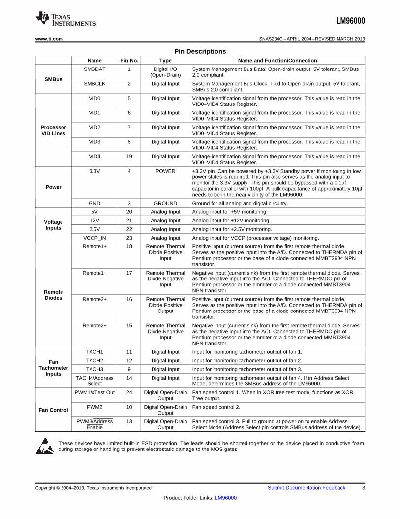
Pin DescriptionsName Pin No. Type Name and Function/Connection
SMBDAT 1 Digital I/O System Management Bus Data. Open-drain output. 5V tolerant, SMBus(Open-Drain) 2.0 compliant.
SMBusSMBCLK 2 Digital Input System Management Bus Clock. Tied to Open-drain output. 5V tolerant,
SMBus 2.0 compliant.
VID0 5 Digital Input Voltage identification signal from the processor. This value is read in theVID0–VID4 Status Register.
VID1 6 Digital Input Voltage identification signal from the processor. This value is read in theVID0–VID4 Status Register.
Processor VID2 7 Digital Input Voltage identification signal from the processor. This value is read in theVID Lines VID0–VID4 Status Register.
VID3 8 Digital Input Voltage identification signal from the processor. This value is read in theVID0–VID4 Status Register.
VID4 19 Digital Input Voltage identification signal from the processor. This value is read in theVID0–VID4 Status Register.
3.3V 4 POWER +3.3V pin. Can be powered by +3.3V Standby power if monitoring in lowpower states is required. This pin also serves as the analog input tomonitor the 3.3V supply. This pin should be bypassed with a 0.1µf
Power capacitor in parallel with 100pf. A bulk capacitance of approximately 10µfneeds to be in the near vicinity of the LM96000.
GND 3 GROUND Ground for all analog and digital circuitry.
5V 20 Analog Input Analog input for +5V monitoring.
12V 21 Analog Input Analog input for +12V monitoring.VoltageInputs 2.5V 22 Analog Input Analog input for +2.5V monitoring.
VCCP_IN 23 Analog Input Analog input for VCCP (processor voltage) monitoring.
Remote1+ 18 Remote Thermal Positive input (current source) from the first remote thermal diode.Diode Positive Serves as the positive input into the A/D. Connected to THERMDA pin of
Input Pentium processor or the base of a diode connected MMBT3904 NPNtransistor.
Remote1− 17 Remote Thermal Negative input (current sink) from the first remote thermal diode. ServesDiode Negative as the negative input into the A/D. Connected to THERMDC pin of
Input Pentium processor or the emmiter of a diode connected MMBT3904NPN transistor.Remote
Diodes Remote2+ 16 Remote Thermal Positive input (current source) from the first remote thermal diode.Diode Positive Serves as the positive input into the A/D. Connected to THERMDA pin of
Output Pentium processor or the base of a diode connected MMBT3904 NPNtransistor.
Remote2− 15 Remote Thermal Negative input (current sink) from the first remote thermal diode. ServesDiode Negative as the negative input into the A/D. Connected to THERMDC pin of
Input Pentium processor or the emmiter of a diode connected MMBT3904NPN transistor.
TACH1 11 Digital Input Input for monitoring tachometer output of fan 1.
TACH2 12 Digital Input Input for monitoring tachometer output of fan 2.FanTachometer TACH3 9 Digital Input Input for monitoring tachometer output of fan 3.
InputsTACH4/Address 14 Digital Input Input for monitoring tachometer output of fan 4. If in Address Select
Select Mode, determines the SMBus address of the LM96000.
PWM1/xTest Out 24 Digital Open-Drain Fan speed control 1. When in XOR tree test mode, functions as XOROutput Tree output.
PWM2 10 Digital Open-Drain Fan speed control 2.Fan Control Output
PWM3/Address 13 Digital Open-Drain Fan speed control 3. Pull to ground at power on to enable AddressEnable Output Select Mode (Address Select pin controls SMBus address of the device).
These devices have limited built-in ESD protection. The leads should be shorted together or the device placed in conductive foamduring storage or handling to prevent electrostatic damage to the MOS gates.
Copyright © 2004–2013, Texas Instruments Incorporated Submit Documentation Feedback 3
Product Folder Links: LM96000
LM96000
SNAS234C –APRIL 2004–REVISED MARCH 2013 www.ti.com
Absolute Maximum Ratings (1) (2) (3)
Supply Voltage, V+ −0.5V to 6.0V
Voltage on Any Digital Input or −0.5V to 6.0VOutput Pin
Voltage on 12V Analog Input −0.5V to 16V
Voltage on 5V Analog Input −0.5V to 6.66V
Voltage on Remote1+, Remote2+, −0.5V to (V+ + 0.05V)
Current on Remote1−, Remote2− ±1 mA
Voltage on Other Analog Inputs −0.5V to 6.0V
Input Current on Any Pin (4) ±5 mA
Package Input Current (4) ±20 mA
Package Dissipation at TA = 25°C See (5)
ESD Susceptibility (6) Human Body Model 2500V
Machine Model 250V
Storage Temperature −65°C to +150°C
Soldering process must comply with reflow temperature profile specifications. See www.ti.com/packaging (7)
(1) Absolute Maximum Ratings indicate limits beyond which damage to the device may occur. Operating Ratings indicate conditions forwhich the device is functional, but do not ensure specific performance limits. For ensured specifications and test conditions, see theElectrical Characteristics. The ensured specifications apply only for the test conditions listed. Some performance characteristics maydegrade when the device is not operated under the listed test conditions.
(2) All voltages are measured with respect to GND, unless otherwise noted.(3) If Military/Aerospace specified devices are required, please contact the TI Sales Office/ Distributors for availability and specifications.(4) When the input voltage (VIN) at any pin exceeds the power supplies (VIN < GND or VIN >V+ ), the current at that pin should be limited to
5mA. The 20mA maximum package input current rating limits the number of pins that can safely exceed the power supplies with aninput current of 5mA to four. Parasitic components and/or ESD protection circuitry are shown below for the LM96000's pins. The nominalbreakdown voltage the zener is 6.5V. Care should be taken not to forward bias the parasitic diode D1 present on pins D+ and D−. Doingso by more that 50 mV may corrupt temperature measurements. SNP stands for snap-back device.
(5) Thermal resistance junction-to-ambient when attached to a double-sided printed circuit board with 1 oz. foil is 113 °C/W.(6) Human body model, 100pF discharged through a 1.5kΩ resistor. Machine model, 200pF discharged directly into each pin.(7) Reflow temperature profiles are different for packages containing lead (Pb) than for those that do not.
Operating Ratings (1) (2)
LM96000 Operating Temperature Range 0°C ≤ TA ≤ +85°C
Remote Diode Temperature Range 0°C ≤ TD ≤ +125°C
Supply Voltage (3.3V nominal) +3.0V to +3.6V
VIN Voltage Range
+12V VIN −0.05V to 16V
+5V VIN −0.05V to 6.66V
+3.3V VIN 3.0V to 4.4V
VCCP_IN and All Other Inputs −0.05V to (V+ + 0.05V)
VID0–VID4 −0.05V to 5.5V
Typical Supply Current 0.53 mA
(1) Absolute Maximum Ratings indicate limits beyond which damage to the device may occur. Operating Ratings indicate conditions forwhich the device is functional, but do not ensure specific performance limits. For ensured specifications and test conditions, see theElectrical Characteristics. The ensured specifications apply only for the test conditions listed. Some performance characteristics maydegrade when the device is not operated under the listed test conditions.
(2) All voltages are measured with respect to GND, unless otherwise noted.
4 Submit Documentation Feedback Copyright © 2004–2013, Texas Instruments Incorporated
Product Folder Links: LM96000
LM96000
www.ti.com SNAS234C –APRIL 2004–REVISED MARCH 2013
DC Electrical CharacteristicsThe following specifications apply for V+ = 3.0V to 3.6V, and all analog input source impedance RS = 50Ω unless otherwisespecified in conditions. Boldface limits apply for TA = TJ over TMIN =0°C to TMAX=85°C; all other limits TA =TJ= 25°C. TA isthe ambient temperature of the LM96000; TJ is the junction temperature of the LM96000; TD is the thermal diode junctiontemperature.
Typical Limits UnitsParameter Test Conditions (1) (2) (Limits)
POWER SUPPLY CHARACTERISTICS
Supply Current (3) Converting, Interface and 1.8 3.5 mA (max)Fans Inactive, Peak Current
Converting, Interface and 0.53 mAFans Inactive, AverageCurrent
Power-On Reset Threshold Voltage 1.6 V (min)
2.8 V (max)
TEMPERATURE TO DIGITAL CONVERTER CHARACTERISTICS
Resolution 1 °C8 Bits
Temperature Accuracy (See (4) for Thermal Diode TD=25°C ±2.5 °C (max)Processor Type) TD=0°C to 100°C ±1 ±3 °C (max)
TD=100°C to 125°C ±4 °C (max)
Temperature Accuracy using Internal Diode. (5) See (6) ±1 ±3 °C (max)for the thermal resistance to be used in the self-heating calculation.
IDS External Diode Current Source High Level 188 280 µA (max)
Low Level 11.75 µA
External Diode Current Ratio 16
ANALOG TO DIGITAL CONVERTER CHARACTERISTICS
TUE Total Unadjusted Error (7) ±2 %FS(max)
DNL Differential Non-linearity 1 LSB
Power Supply Sensitivity ±1 %/V
Total Monitoring Cycle Time (8) All Voltage and Temperature 182 200 ms (max)readings
Input Resistance, all analog inputs 210 140 kΩ (min)
400 kΩ (max)
DIGITAL OUTPUT: PWM1, PWM2, PWM3, XTESTOUT
IOL Logic Low Sink Current VOL=0.4V 8 mA (min)
VOL Logic Low Level IOUT = +8 mA 0.4 V (max)
(1) Typicals are at TA = 25°C and represent most likely parametric norm.(2) Limits are specified to TI's AOQL (Average Outgoing Quality Level).(3) The average current can be calculated from the peak current using the following equation:Quiescent current will not increase
substantially with an SMBus transaction.(4) The accuracy of the LM96000CIMT is ensured when using the thermal diode of Intel Pentium 4 90nm processors or any thermal diode
with a non-ideality of 1.011 and series resistance of 3.33Ω. When using a 2N3904 type transistor as a thermal diode the error band willbe typically shifted by -?°C.
(5) Local temperature accuracy does not include the effects of self-heating. The rise in temperature due to self-heating is the product of theinternal power dissipation of the LM96000 and the thermal resistance.
(6) Thermal resistance junction-to-ambient when attached to a double-sided printed circuit board with 1 oz. foil is 113 °C/W.(7) TUE , total unadjusted error, includes ADC gain, offset, linearity and reference errors. TUE is defined as the "actual Vin" to achieve a
given code transition minus the "theoretical Vin" for the same code. Therefore, a positive error indicates that the input voltage is greaterthan the theoretical input voltage for a given code. If the theoretical input voltage was applied to an LM96000 that has positive error, theLM96000's reading would be less than the theoretical.
(8) This specification is provided only to indicate how often temperature and voltage data is updated. The LM96000 can be read at any timewithout regard to conversion state (and will yield last conversion result).
Copyright © 2004–2013, Texas Instruments Incorporated Submit Documentation Feedback 5
Product Folder Links: LM96000
LM96000
SNAS234C –APRIL 2004–REVISED MARCH 2013 www.ti.com
DC Electrical Characteristics (continued)The following specifications apply for V+ = 3.0V to 3.6V, and all analog input source impedance RS = 50Ω unless otherwisespecified in conditions. Boldface limits apply for TA = TJ over TMIN =0°C to TMAX=85°C; all other limits TA =TJ= 25°C. TA isthe ambient temperature of the LM96000; TJ is the junction temperature of the LM96000; TD is the thermal diode junctiontemperature.
Typical Limits UnitsParameter Test Conditions (1) (2) (Limits)
SMBUS OPEN-DRAIN OUTPUT: SMBDAT
VOL Logic Low Output Voltage IOUT = +4 mA 0.4V V (max)
IOH High Level Output Current VOUT = V+ 0.1 10 µA (max)
SMBUS INPUTS: SMBCLK. SMBDAT
VIH Logic Input High Voltage 2.1 V (min)
VIL Logic Input Low Voltage 0.8 V (max)
VHYST Logic Input Hysteresis Voltage 300 mV
DIGITAL INPUTS: ALL
VIH Logic Input High Voltage 2.1 V (min)
VIL Logic Input Low Voltage 0.8 V (max)
VTH Logic Input Threshold Voltage 1.5 V
IIH Logic High Input Current VIN = V+ 0.005 10 µA (max)
IIL Logic Low Input Current VIN = GND −0.005 −10 µA (max)
CIN Digital Input Capacitance 20 pF
AC Electrical CharacteristicsThe following specifications apply for V+ = 3.0V to 3.6V unless otherwise specified in conditions. Boldface limits apply forTA = TJ over TMIN =0°C to TMAX=85°C; all other limits TA =TJ= 25°C.
Typical Limits UnitsParameter Test Conditions (1) (2) (Limits)
TACHOMETER ACCURACY
Fan Count Accuracy ±10 % (max)
Fan Full-Scale Count 65536 (max)
Fan Counter Clock Frequency 90 kHz
Fan Count Conversion Time 0.7 1.4 sec (max)
FAN PWM OUTPUT
Frequency Setting Accuracy ±10 % (max)
Frequency Range 10 Hz30 kHz
Duty-Cycle Range Low frequency range 0 to 100 % (max)
Duty-Cycle Resolution (8-bits) 0.390625 %
Spin-Up Time Interval Range 100 ms4000 ms
Spin-Up Time Interval Accuracy ±10 % (max)
SPIKE SMOOTHING FILTER
Time Interval Deviation ±10 % (max)
Time Interval Range 35 sec0.8 sec
(1) Typicals are at TA = 25°C and represent most likely parametric norm.(2) Limits are specified to TI's AOQL (Average Outgoing Quality Level).
6 Submit Documentation Feedback Copyright © 2004–2013, Texas Instruments Incorporated
Product Folder Links: LM96000
SNP
GND
D1
PIN
VIH
VIL
SMBCLK
P
S
VIH
VIL
SMBDAT
tBUFtHD;STA
tLOW
tR
tHD;DAT
tHIGH
tF
tSU;DATtSU;STA tSU;STO
PS
LM96000
www.ti.com SNAS234C –APRIL 2004–REVISED MARCH 2013
AC Electrical Characteristics (continued)The following specifications apply for V+ = 3.0V to 3.6V unless otherwise specified in conditions. Boldface limits apply forTA = TJ over TMIN =0°C to TMAX=85°C; all other limits TA =TJ= 25°C.
Typical Limits UnitsParameter Test Conditions (1) (2) (Limits)
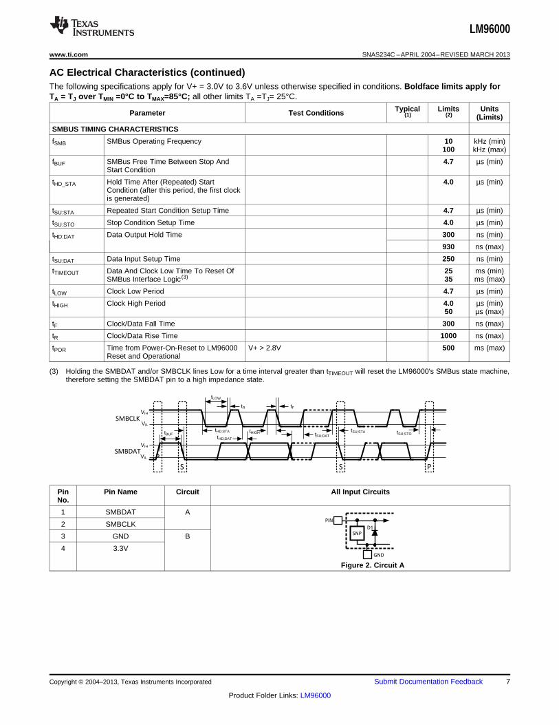
SMBUS TIMING CHARACTERISTICS
fSMB SMBus Operating Frequency 10 kHz (min)100 kHz (max)
fBUF SMBus Free Time Between Stop And 4.7 µs (min)Start Condition
tHD_STA Hold Time After (Repeated) Start 4.0 µs (min)Condition (after this period, the first clockis generated)
tSU:STA Repeated Start Condition Setup Time 4.7 µs (min)
tSU:STO Stop Condition Setup Time 4.0 µs (min)
tHD:DAT Data Output Hold Time 300 ns (min)
930 ns (max)
tSU:DAT Data Input Setup Time 250 ns (min)
tTIMEOUT Data And Clock Low Time To Reset Of 25 ms (min)SMBus Interface Logic (3) 35 ms (max)
tLOW Clock Low Period 4.7 µs (min)
tHIGH Clock High Period 4.0 µs (min)50 µs (max)
tF Clock/Data Fall Time 300 ns (max)
tR Clock/Data Rise Time 1000 ns (max)
tPOR Time from Power-On-Reset to LM96000 V+ > 2.8V 500 ms (max)Reset and Operational
(3) Holding the SMBDAT and/or SMBCLK lines Low for a time interval greater than tTIMEOUT will reset the LM96000's SMBus state machine,therefore setting the SMBDAT pin to a high impedance state.
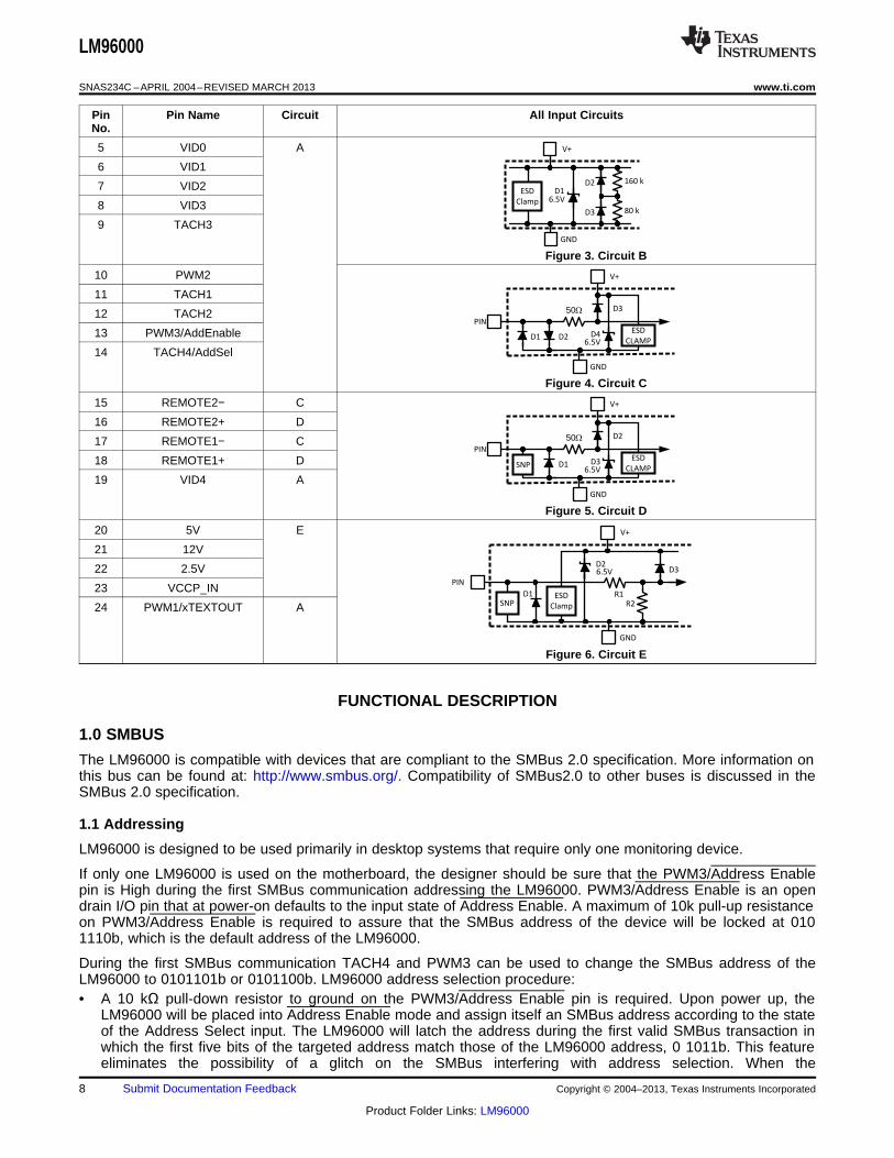
Pin Pin Name Circuit All Input CircuitsNo.
1 SMBDAT A
2 SMBCLK
3 GND B
4 3.3V
Figure 2. Circuit A
Copyright © 2004–2013, Texas Instruments Incorporated Submit Documentation Feedback 7
Product Folder Links: LM96000
SNP
V+
GND
D1 R1ESD
Clamp
D3
PIN
D26.5V
R2
GND
PIN
D1
V+
6.5V
D3ESD
CLAMP
50: D2
SNP
GND
D1
PIN
D2
V+
6.5V
D4ESD
CLAMP
50: D3
V+
GND
ESD
Clamp 6.5VD1
D2
D3
160 k
80 k
LM96000
SNAS234C –APRIL 2004–REVISED MARCH 2013 www.ti.com
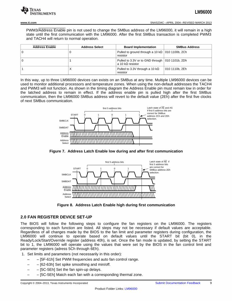
Pin Pin Name Circuit All Input CircuitsNo.
5 VID0 A
6 VID1
7 VID2
8 VID3
9 TACH3
Figure 3. Circuit B
10 PWM2
11 TACH1
12 TACH2
13 PWM3/AddEnable
14 TACH4/AddSel
Figure 4. Circuit C
15 REMOTE2− C
16 REMOTE2+ D
17 REMOTE1− C
18 REMOTE1+ D
19 VID4 A
Figure 5. Circuit D
20 5V E
21 12V
22 2.5V
23 VCCP_IN
24 PWM1/xTEXTOUT A
Figure 6. Circuit E
FUNCTIONAL DESCRIPTION
1.0 SMBUS
The LM96000 is compatible with devices that are compliant to the SMBus 2.0 specification. More information onthis bus can be found at: http://www.smbus.org/. Compatibility of SMBus2.0 to other buses is discussed in theSMBus 2.0 specification.
1.1 Addressing
LM96000 is designed to be used primarily in desktop systems that require only one monitoring device.
If only one LM96000 is used on the motherboard, the designer should be sure that the PWM3/Address Enablepin is High during the first SMBus communication addressing the LM96000. PWM3/Address Enable is an opendrain I/O pin that at power-on defaults to the input state of Address Enable. A maximum of 10k pull-up resistanceon PWM3/Address Enable is required to assure that the SMBus address of the device will be locked at 0101110b, which is the default address of the LM96000.
During the first SMBus communication TACH4 and PWM3 can be used to change the SMBus address of theLM96000 to 0101101b or 0101100b. LM96000 address selection procedure:• A 10 kΩ pull-down resistor to ground on the PWM3/Address Enable pin is required. Upon power up, the
LM96000 will be placed into Address Enable mode and assign itself an SMBus address according to the stateof the Address Select input. The LM96000 will latch the address during the first valid SMBus transaction inwhich the first five bits of the targeted address match those of the LM96000 address, 0 1011b. This featureeliminates the possibility of a glitch on the SMBus interfering with address selection. When the
8 Submit Documentation Feedback Copyright © 2004–2013, Texas Instruments Incorporated
Product Folder Links: LM96000
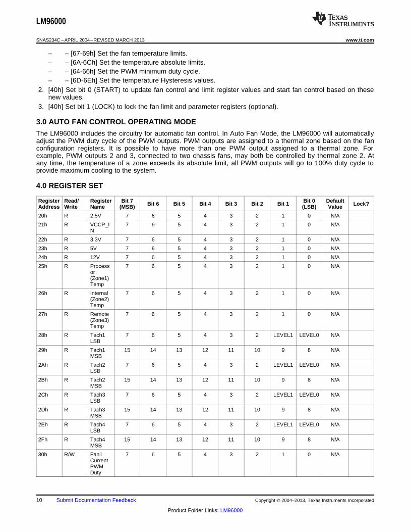
SMBDAT
SMBCLK
Address Enable
Address Select
START 0 1 0 1 1
first 5 address bits Latch state of AE if first 5 address bits are correct for SMBus address 2Eh selection.
SMBDAT
SMBCLK
Address Enable
Address Select
START 0 1 0 1 1
first 5 address bits Latch state of AE and AS if first 5 address bits are correct for SMBus address 2Ch and 2Dh selection.
LM96000
www.ti.com SNAS234C –APRIL 2004–REVISED MARCH 2013
PWM3/Address Enable pin is not used to change the SMBus address of the LM96000, it will remain in a highstate until the first communication with the LM96000. After the first SMBus transaction is completed PWM3and TACH4 will return to normal operation.
Address Enable Address Select Board Implementation SMBus Address
0 0 Pulled to ground through a 10 kΩ 010 1100b, 2Chresistor
0 1 Pulled to 3.3V or to GND through 010 1101b, 2Dha 10 kΩ resistor
1 X Pulled to 3.3V through a 10 kΩ 010 1110b, 2Ehresistor
In this way, up to three LM96000 devices can exists on an SMBus at any time. Multiple LM96000 devices can beused to monitor additional processors and temperature zones. When using the non-default addresses the TACH4and PWM3 will not function. As shown in the timing diagram the Address Enable pin must remain low in order forthe latched address to remain in effect. If the address enable pin is pulled high after the first SMBuscommunication, then the LM96000 SMBus address will revert to the default value (2Eh) after the first five clocksof next SMBus communication.
Figure 7. Address Latch Enable low during and after first communication
Figure 8. Address Latch Enable high during first communication
2.0 FAN REGISTER DEVICE SET-UP
The BIOS will follow the following steps to configure the fan registers on the LM96000. The registerscorresponding to each function are listed. All steps may not be necessary if default values are acceptable.Regardless of all changes made by the BIOS to the fan limit and parameter registers during configuration, theLM96000 will continue to operate based on default values until the START bit (bit 0), in theReady/Lock/Start/Override register (address 40h), is set. Once the fan mode is updated, by setting the STARTbit to 1, the LM96000 will operate using the values that were set by the BIOS in the fan control limit andparameter registers (adress 5Ch through 6Eh).1. Set limits and parameters (not necessarily in this order):
– – [5F-61h] Set PWM frequencies and auto fan control range.– – [62-63h] Set spike smoothing and min/off.– – [5C-5Eh] Set the fan spin-up delays.– – [5C-5Eh] Match each fan with a corresponding thermal zone.
Copyright © 2004–2013, Texas Instruments Incorporated Submit Documentation Feedback 9
Product Folder Links: LM96000
LM96000
SNAS234C –APRIL 2004–REVISED MARCH 2013 www.ti.com
– – [67-69h] Set the fan temperature limits.– – [6A-6Ch] Set the temperature absolute limits.– – [64-66h] Set the PWM minimum duty cycle.– – [6D-6Eh] Set the temperature Hysteresis values.
2. [40h] Set bit 0 (START) to update fan control and limit register values and start fan control based on thesenew values.
3. [40h] Set bit 1 (LOCK) to lock the fan limit and parameter registers (optional).
3.0 AUTO FAN CONTROL OPERATING MODE
The LM96000 includes the circuitry for automatic fan control. In Auto Fan Mode, the LM96000 will automaticallyadjust the PWM duty cycle of the PWM outputs. PWM outputs are assigned to a thermal zone based on the fanconfiguration registers. It is possible to have more than one PWM output assigned to a thermal zone. Forexample, PWM outputs 2 and 3, connected to two chassis fans, may both be controlled by thermal zone 2. Atany time, the temperature of a zone exceeds its absolute limit, all PWM outputs will go to 100% duty cycle toprovide maximum cooling to the system.
4.0 REGISTER SET
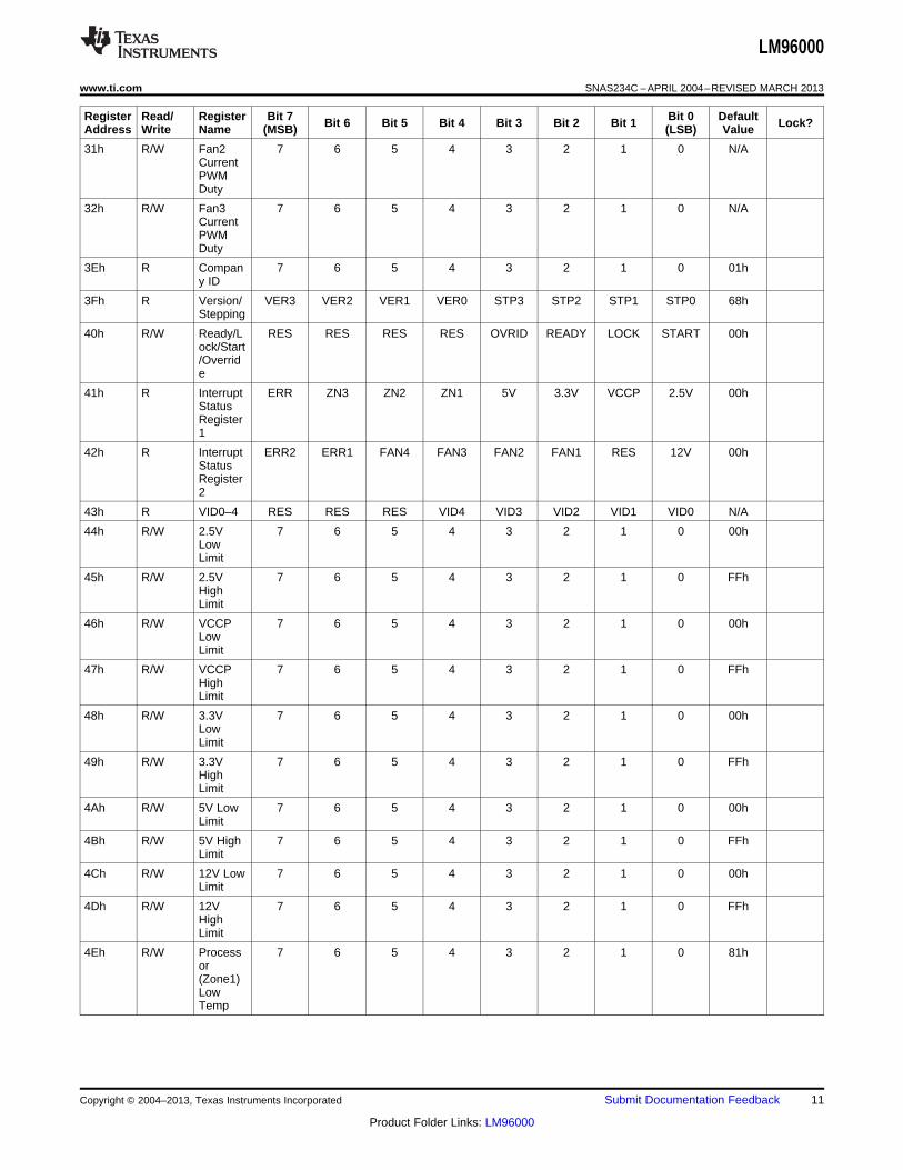
Register Read/ Register Bit 7 Bit 0 DefaultBit 6 Bit 5 Bit 4 Bit 3 Bit 2 Bit 1 Lock?Address Write Name (MSB) (LSB) Value
20h R 2.5V 7 6 5 4 3 2 1 0 N/A
21h R VCCP_I 7 6 5 4 3 2 1 0 N/AN
22h R 3.3V 7 6 5 4 3 2 1 0 N/A
23h R 5V 7 6 5 4 3 2 1 0 N/A
24h R 12V 7 6 5 4 3 2 1 0 N/A
25h R Process 7 6 5 4 3 2 1 0 N/Aor(Zone1)Temp
26h R Internal 7 6 5 4 3 2 1 0 N/A(Zone2)Temp
27h R Remote 7 6 5 4 3 2 1 0 N/A(Zone3)Temp
28h R Tach1 7 6 5 4 3 2 LEVEL1 LEVEL0 N/ALSB
29h R Tach1 15 14 13 12 11 10 9 8 N/AMSB
2Ah R Tach2 7 6 5 4 3 2 LEVEL1 LEVEL0 N/ALSB
2Bh R Tach2 15 14 13 12 11 10 9 8 N/AMSB
2Ch R Tach3 7 6 5 4 3 2 LEVEL1 LEVEL0 N/ALSB
2Dh R Tach3 15 14 13 12 11 10 9 8 N/AMSB
2Eh R Tach4 7 6 5 4 3 2 LEVEL1 LEVEL0 N/ALSB
2Fh R Tach4 15 14 13 12 11 10 9 8 N/AMSB
30h R/W Fan1 7 6 5 4 3 2 1 0 N/ACurrentPWMDuty
10 Submit Documentation Feedback Copyright © 2004–2013, Texas Instruments Incorporated
Product Folder Links: LM96000
LM96000
www.ti.com SNAS234C –APRIL 2004–REVISED MARCH 2013
Register Read/ Register Bit 7 Bit 0 DefaultBit 6 Bit 5 Bit 4 Bit 3 Bit 2 Bit 1 Lock?Address Write Name (MSB) (LSB) Value
31h R/W Fan2 7 6 5 4 3 2 1 0 N/ACurrentPWMDuty
32h R/W Fan3 7 6 5 4 3 2 1 0 N/ACurrentPWMDuty
3Eh R Compan 7 6 5 4 3 2 1 0 01hy ID
3Fh R Version/ VER3 VER2 VER1 VER0 STP3 STP2 STP1 STP0 68hStepping
40h R/W Ready/L RES RES RES RES OVRID READY LOCK START 00hock/Start/Override
41h R Interrupt ERR ZN3 ZN2 ZN1 5V 3.3V VCCP 2.5V 00hStatusRegister1
42h R Interrupt ERR2 ERR1 FAN4 FAN3 FAN2 FAN1 RES 12V 00hStatusRegister2
43h R VID0–4 RES RES RES VID4 VID3 VID2 VID1 VID0 N/A
44h R/W 2.5V 7 6 5 4 3 2 1 0 00hLowLimit
45h R/W 2.5V 7 6 5 4 3 2 1 0 FFhHighLimit
46h R/W VCCP 7 6 5 4 3 2 1 0 00hLowLimit
47h R/W VCCP 7 6 5 4 3 2 1 0 FFhHighLimit
48h R/W 3.3V 7 6 5 4 3 2 1 0 00hLowLimit
49h R/W 3.3V 7 6 5 4 3 2 1 0 FFhHighLimit
4Ah R/W 5V Low 7 6 5 4 3 2 1 0 00hLimit
4Bh R/W 5V High 7 6 5 4 3 2 1 0 FFhLimit
4Ch R/W 12V Low 7 6 5 4 3 2 1 0 00hLimit
4Dh R/W 12V 7 6 5 4 3 2 1 0 FFhHighLimit
4Eh R/W Process 7 6 5 4 3 2 1 0 81hor(Zone1)LowTemp
Copyright © 2004–2013, Texas Instruments Incorporated Submit Documentation Feedback 11
Product Folder Links: LM96000
LM96000
SNAS234C –APRIL 2004–REVISED MARCH 2013 www.ti.com
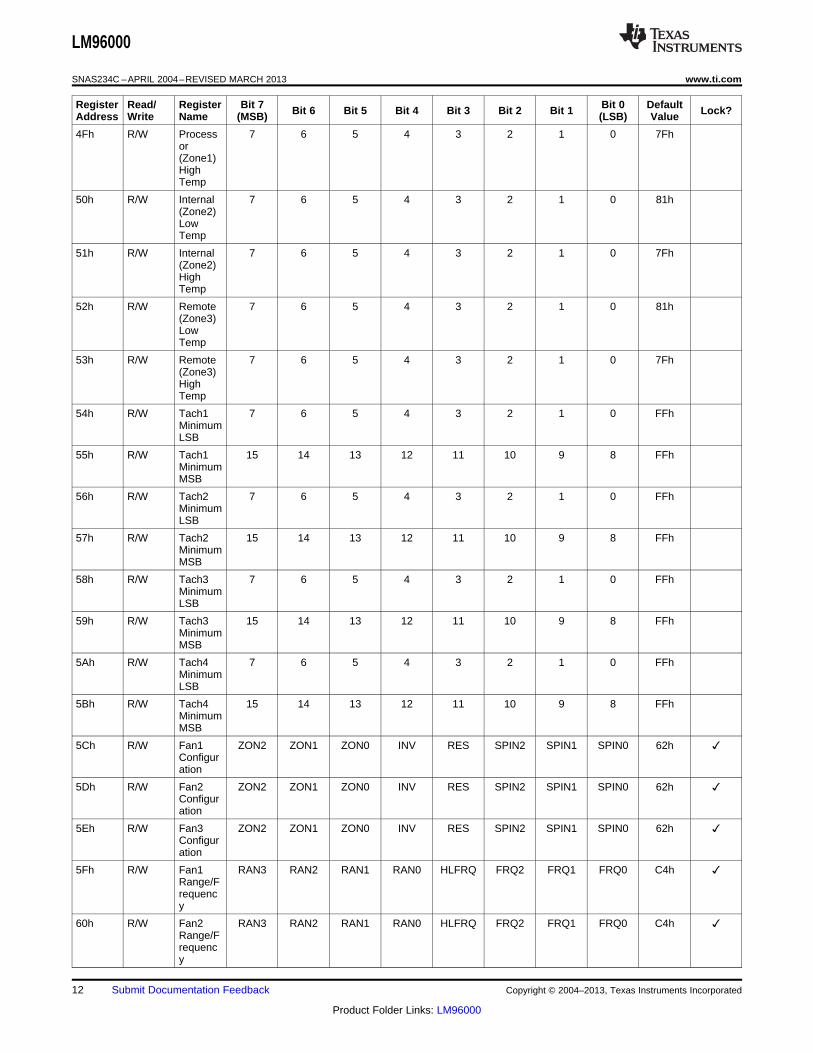
Register Read/ Register Bit 7 Bit 0 DefaultBit 6 Bit 5 Bit 4 Bit 3 Bit 2 Bit 1 Lock?Address Write Name (MSB) (LSB) Value
4Fh R/W Process 7 6 5 4 3 2 1 0 7Fhor(Zone1)HighTemp
50h R/W Internal 7 6 5 4 3 2 1 0 81h(Zone2)LowTemp
51h R/W Internal 7 6 5 4 3 2 1 0 7Fh(Zone2)HighTemp
52h R/W Remote 7 6 5 4 3 2 1 0 81h(Zone3)LowTemp
53h R/W Remote 7 6 5 4 3 2 1 0 7Fh(Zone3)HighTemp
54h R/W Tach1 7 6 5 4 3 2 1 0 FFhMinimumLSB
55h R/W Tach1 15 14 13 12 11 10 9 8 FFhMinimumMSB
56h R/W Tach2 7 6 5 4 3 2 1 0 FFhMinimumLSB
57h R/W Tach2 15 14 13 12 11 10 9 8 FFhMinimumMSB
58h R/W Tach3 7 6 5 4 3 2 1 0 FFhMinimumLSB
59h R/W Tach3 15 14 13 12 11 10 9 8 FFhMinimumMSB
5Ah R/W Tach4 7 6 5 4 3 2 1 0 FFhMinimumLSB
5Bh R/W Tach4 15 14 13 12 11 10 9 8 FFhMinimumMSB
5Ch R/W Fan1 ZON2 ZON1 ZON0 INV RES SPIN2 SPIN1 SPIN0 62h Configuration
5Dh R/W Fan2 ZON2 ZON1 ZON0 INV RES SPIN2 SPIN1 SPIN0 62h Configuration
5Eh R/W Fan3 ZON2 ZON1 ZON0 INV RES SPIN2 SPIN1 SPIN0 62h Configuration
5Fh R/W Fan1 RAN3 RAN2 RAN1 RAN0 HLFRQ FRQ2 FRQ1 FRQ0 C4h Range/Frequency
60h R/W Fan2 RAN3 RAN2 RAN1 RAN0 HLFRQ FRQ2 FRQ1 FRQ0 C4h Range/Frequency
12 Submit Documentation Feedback Copyright © 2004–2013, Texas Instruments Incorporated
Product Folder Links: LM96000
LM96000
www.ti.com SNAS234C –APRIL 2004–REVISED MARCH 2013
Register Read/ Register Bit 7 Bit 0 DefaultBit 6 Bit 5 Bit 4 Bit 3 Bit 2 Bit 1 Lock?Address Write Name (MSB) (LSB) Value
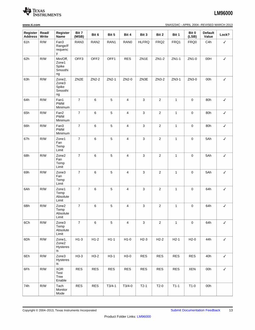
61h R/W Fan3 RAN3 RAN2 RAN1 RAN0 HLFRQ FRQ2 FRQ1 FRQ0 C4h Range/Frequency
62h R/W Min/Off, OFF3 OFF2 OFF1 RES ZN1E ZN1-2 ZN1-1 ZN1-0 00H Zone1SpikeSmoothing
63h R/W Zone2, ZN2E ZN2-2 ZN2-1 ZN2-0 ZN3E ZN3-2 ZN3-1 ZN3-0 00h Zone3SpikeSmoothing
64h R/W Fan1 7 6 5 4 3 2 1 0 80h PWMMinimum
65h R/W Fan2 7 6 5 4 3 2 1 0 80h PWMMinimum
66h R/W Fan3 7 6 5 4 3 2 1 0 80h PWMMinimum
67h R/W Zone1 7 6 5 4 3 2 1 0 5Ah FanTempLimit
68h R/W Zone2 7 6 5 4 3 2 1 0 5Ah FanTempLimit
69h R/W Zone3 7 6 5 4 3 2 1 0 5Ah FanTempLimit
6Ah R/W Zone1 7 6 5 4 3 2 1 0 64h TempAbsoluteLimit
6Bh R/W Zone2 7 6 5 4 3 2 1 0 64h TempAbsoluteLimit
6Ch R/W Zone3 7 6 5 4 3 2 1 0 64h TempAbsoluteLimit
6Dh R/W Zone1, H1-3 H1-2 H1-1 H1-0 H2-3 H2-2 H2-1 H2-0 44h Zone2Hysteresis
6Eh R/W Zone3 H3-3 H3-2 H3-1 H3-0 RES RES RES RES 40h Hysteresis
6Fh R/W XOR RES RES RES RES RES RES RES XEN 00h TestTreeEnable
74h R/W Tach RES RES T3/4-1 T3/4-0 T2-1 T2-0 T1-1 T1-0 00hMonitorMode
Copyright © 2004–2013, Texas Instruments Incorporated Submit Documentation Feedback 13
Product Folder Links: LM96000
LM96000
SNAS234C –APRIL 2004–REVISED MARCH 2013 www.ti.com
Register Read/ Register Bit 7 Bit 0 DefaultBit 6 Bit 5 Bit 4 Bit 3 Bit 2 Bit 1 Lock?Address Write Name (MSB) (LSB) Value
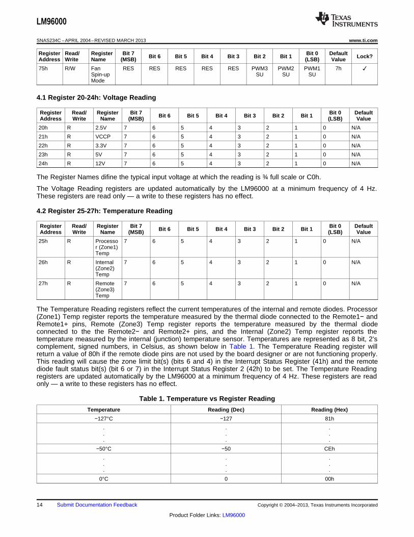
75h R/W Fan RES RES RES RES RES PWM3 PWM2 PWM1 7h Spin-up SU SU SUMode
4.1 Register 20-24h: Voltage Reading
Register Read/ Register Bit 7 Bit 0 DefaultBit 6 Bit 5 Bit 4 Bit 3 Bit 2 Bit 1Address Write Name (MSB) (LSB) Value
20h R 2.5V 7 6 5 4 3 2 1 0 N/A
21h R VCCP 7 6 5 4 3 2 1 0 N/A
22h R 3.3V 7 6 5 4 3 2 1 0 N/A
23h R 5V 7 6 5 4 3 2 1 0 N/A
24h R 12V 7 6 5 4 3 2 1 0 N/A
The Register Names difine the typical input voltage at which the reading is ¾ full scale or C0h.
The Voltage Reading registers are updated automatically by the LM96000 at a minimum frequency of 4 Hz.These registers are read only — a write to these registers has no effect.
4.2 Register 25-27h: Temperature Reading
Register Read/ Register Bit 7 Bit 0 DefaultBit 6 Bit 5 Bit 4 Bit 3 Bit 2 Bit 1Address Write Name (MSB) (LSB) Value
25h R Processo 7 6 5 4 3 2 1 0 N/Ar (Zone1)Temp
26h R Internal 7 6 5 4 3 2 1 0 N/A(Zone2)Temp
27h R Remote 7 6 5 4 3 2 1 0 N/A(Zone3)Temp
The Temperature Reading registers reflect the current temperatures of the internal and remote diodes. Processor(Zone1) Temp register reports the temperature measured by the thermal diode connected to the Remote1− andRemote1+ pins, Remote (Zone3) Temp register reports the temperature measured by the thermal diodeconnected to the the Remote2− and Remote2+ pins, and the Internal (Zone2) Temp register reports thetemperature measured by the internal (junction) temperature sensor. Temperatures are represented as 8 bit, 2’scomplement, signed numbers, in Celsius, as shown below in Table 1. The Temperature Reading register willreturn a value of 80h if the remote diode pins are not used by the board designer or are not functioning properly.This reading will cause the zone limit bit(s) (bits 6 and 4) in the Interrupt Status Register (41h) and the remotediode fault status bit(s) (bit 6 or 7) in the Interrupt Status Register 2 (42h) to be set. The Temperature Readingregisters are updated automatically by the LM96000 at a minimum frequency of 4 Hz. These registers are readonly — a write to these registers has no effect.
Table 1. Temperature vs Register Reading
Temperature Reading (Dec) Reading (Hex)
−127°C −127 81h
. . .
. . .
. . .
−50°C −50 CEh
. . .
. . .
. . .
0°C 0 00h
14 Submit Documentation Feedback Copyright © 2004–2013, Texas Instruments Incorporated
Product Folder Links: LM96000
LM96000
www.ti.com SNAS234C –APRIL 2004–REVISED MARCH 2013
Table 1. Temperature vs Register Reading (continued)
Temperature Reading (Dec) Reading (Hex)
. . .
. . .
. . .
127°C 127 7Fh
(SENSOR ERROR) 80h
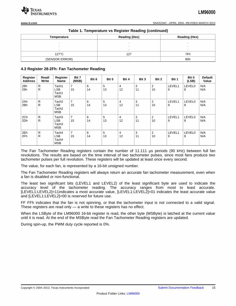
4.3 Register 28-2Fh: Fan Tachometer Reading
Register Read/ Register Bit 7 Bit 0 DefaultBit 6 Bit 5 Bit 4 Bit 3 Bit 2 Bit 1Address Write Name (MSB) (LSB) Value
28h R Tach1 7 6 5 4 3 2 LEVEL1 LEVEL0 N/A29h R LSB 15 14 13 12 11 10 9 8 N/A
Tach1MSB
2Ah R Tach2 7 6 5 4 3 2 LEVEL1 LEVEL0 N/A2Bh R LSB 15 14 13 12 11 10 9 8 N/A
Tach2MSB
2Ch R Tach3 7 6 5 4 3 2 LEVEL1 LEVEL0 N/A2Dh R LSB 15 14 13 12 11 10 9 8 N/A
Tach3MSB
2Eh R Tach4 7 6 5 4 3 2 LEVEL1 LEVEL0 N/A2Fh R LSB 15 14 13 12 11 10 9 8 N/A
Tach4MSB
The Fan Tachometer Reading registers contain the number of 11.111 µs periods (90 kHz) between full fanrevolutions. The results are based on the time interval of two tachometer pulses, since most fans produce twotachometer pulses per full revolution. These registers will be updated at least once every second.
The value, for each fan, is represented by a 16-bit unsigned number.
The Fan Tachometer Reading registers will always return an accurate fan tachometer measurement, even whena fan is disabled or non-functional.
The least two significant bits (LEVEL1 and LEVEL2) of the least significant byte are used to indicate theaccuracy level of the tachometer reading. The accuracy ranges from most to least accurate.[LEVEL1:LEVEL2]=11indicates a most accurate value, [LEVEL1:LEVEL2]=01 indicates the least accurate valueand [LEVEL1:LEVEL2]=00 is reserved for future use.
FF FFh indicates that the fan is not spinning, or that the tachometer input is not connected to a valid signal.These registers are read only — a write to these registers has no effect.
When the LSByte of the LM96000 16-bit register is read, the other byte (MSByte) is latched at the current valueuntil it is read. At the end of the MSByte read the Fan Tachometer Reading registers are updated.
During spin-up, the PWM duty cycle reported is 0%.
Copyright © 2004–2013, Texas Instruments Incorporated Submit Documentation Feedback 15
Product Folder Links: LM96000
LM96000
SNAS234C –APRIL 2004–REVISED MARCH 2013 www.ti.com
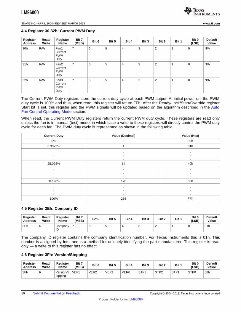
4.4 Register 30-32h: Current PWM Duty
Register Read/ Register Bit 7 Bit 0 DefaultBit 6 Bit 5 Bit 4 Bit 3 Bit 2 Bit 1Address Write Name (MSB) (LSB) Value
30h R/W Fan1 7 6 5 4 3 2 1 0 N/ACurrentPWMDuty
31h R/W Fan2 7 6 5 4 3 2 1 0 N/ACurrentPWMDuty
32h R/W Fan3 7 6 5 4 3 2 1 0 N/ACurrentPWMDuty
The Current PWM Duty registers store the current duty cycle at each PWM output. At initial power-on, the PWMduty cycle is 100% and thus, when read, this register will return FFh. After the Ready/Lock/Start/Override registerStart bit is set, this register and the PWM signals will be updated based on the algorithm described in the AutoFan Control Operating Mode section.
When read, the Current PWM Duty registers return the current PWM duty cycle. These registers are read onlyunless the fan is in manual (test) mode, in which case a write to these registers will directly control the PWM dutycycle for each fan. The PWM duty cycle is represented as shown in the following table.
Current Duty Value (Decimal) Value (Hex)
0% 0 00h
0.3922% 1 01h
. . .
. . .
. . .
25.098% 64 40h
. . .
. . .
. . .
50.196% 128 80h
. . .
. . .
. . .
100% 255 FFh
4.5 Register 3Eh: Company ID
Register Read/ Register Bit 7 Bit 0 DefaultBit 6 Bit 5 Bit 4 Bit 3 Bit 2 Bit 1Address Write Name (MSB) (LSB) Value
3Eh R Company 7 6 5 4 3 2 1 0 01hID
The company ID register contains the company identification number. For Texas Instruments this is 01h. Thisnumber is assigned by Intel and is a method for uniquely identifying the part manufacturer. This register is readonly — a write to this register has no effect.
4.6 Register 3Fh: Version/Stepping
Register Read/ Register Bit 7 Bit 0 DefaultBit 6 Bit 5 Bit 4 Bit 3 Bit 2 Bit 1Address Write Name (MSB) (LSB) Value
3Fh R Version/S VER3 VER2 VER1 VER0 STP3 STP2 STP1 STP0 68htepping
16 Submit Documentation Feedback Copyright © 2004–2013, Texas Instruments Incorporated
Product Folder Links: LM96000
LM96000
www.ti.com SNAS234C –APRIL 2004–REVISED MARCH 2013
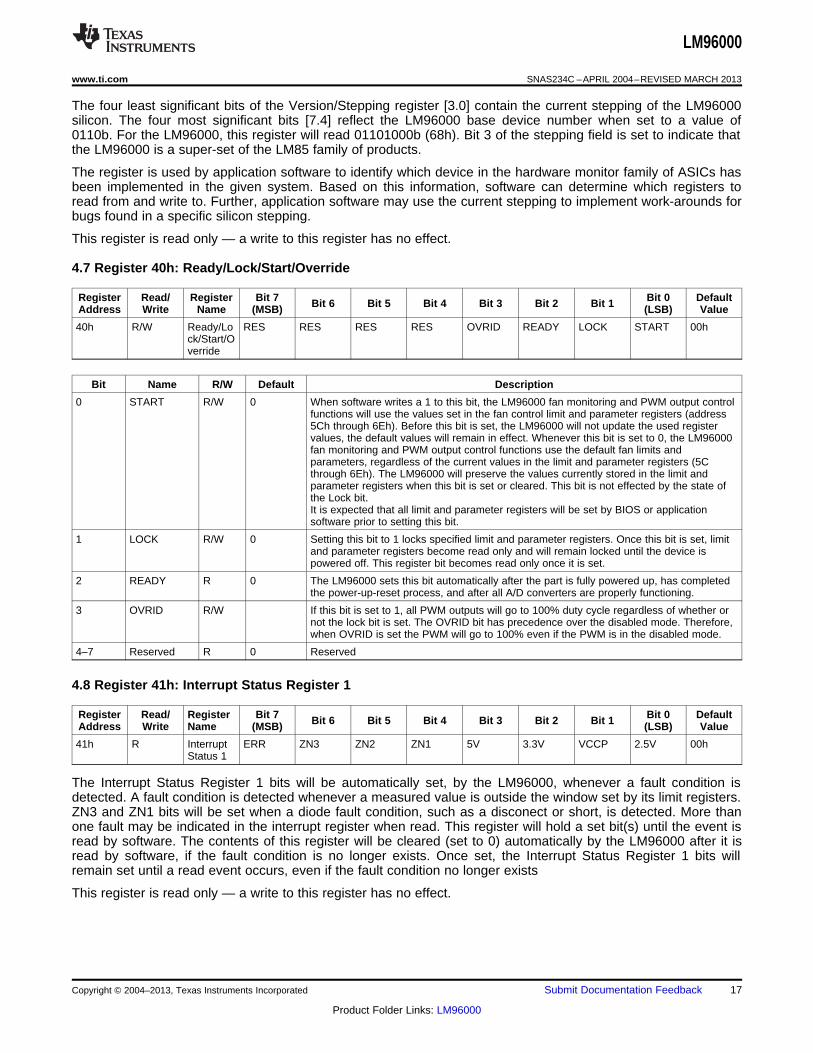
The four least significant bits of the Version/Stepping register [3.0] contain the current stepping of the LM96000silicon. The four most significant bits [7.4] reflect the LM96000 base device number when set to a value of0110b. For the LM96000, this register will read 01101000b (68h). Bit 3 of the stepping field is set to indicate thatthe LM96000 is a super-set of the LM85 family of products.
The register is used by application software to identify which device in the hardware monitor family of ASICs hasbeen implemented in the given system. Based on this information, software can determine which registers toread from and write to. Further, application software may use the current stepping to implement work-arounds forbugs found in a specific silicon stepping.
This register is read only — a write to this register has no effect.
4.7 Register 40h: Ready/Lock/Start/Override
Register Read/ Register Bit 7 Bit 0 DefaultBit 6 Bit 5 Bit 4 Bit 3 Bit 2 Bit 1Address Write Name (MSB) (LSB) Value
40h R/W Ready/Lo RES RES RES RES OVRID READY LOCK START 00hck/Start/Override
Bit Name R/W Default Description
0 START R/W 0 When software writes a 1 to this bit, the LM96000 fan monitoring and PWM output controlfunctions will use the values set in the fan control limit and parameter registers (address5Ch through 6Eh). Before this bit is set, the LM96000 will not update the used registervalues, the default values will remain in effect. Whenever this bit is set to 0, the LM96000fan monitoring and PWM output control functions use the default fan limits andparameters, regardless of the current values in the limit and parameter registers (5Cthrough 6Eh). The LM96000 will preserve the values currently stored in the limit andparameter registers when this bit is set or cleared. This bit is not effected by the state ofthe Lock bit.It is expected that all limit and parameter registers will be set by BIOS or applicationsoftware prior to setting this bit.
1 LOCK R/W 0 Setting this bit to 1 locks specified limit and parameter registers. Once this bit is set, limitand parameter registers become read only and will remain locked until the device ispowered off. This register bit becomes read only once it is set.
2 READY R 0 The LM96000 sets this bit automatically after the part is fully powered up, has completedthe power-up-reset process, and after all A/D converters are properly functioning.
3 OVRID R/W If this bit is set to 1, all PWM outputs will go to 100% duty cycle regardless of whether ornot the lock bit is set. The OVRID bit has precedence over the disabled mode. Therefore,when OVRID is set the PWM will go to 100% even if the PWM is in the disabled mode.
4–7 Reserved R 0 Reserved
4.8 Register 41h: Interrupt Status Register 1
Register Read/ Register Bit 7 Bit 0 DefaultBit 6 Bit 5 Bit 4 Bit 3 Bit 2 Bit 1Address Write Name (MSB) (LSB) Value
41h R Interrupt ERR ZN3 ZN2 ZN1 5V 3.3V VCCP 2.5V 00hStatus 1
The Interrupt Status Register 1 bits will be automatically set, by the LM96000, whenever a fault condition isdetected. A fault condition is detected whenever a measured value is outside the window set by its limit registers.ZN3 and ZN1 bits will be set when a diode fault condition, such as a disconect or short, is detected. More thanone fault may be indicated in the interrupt register when read. This register will hold a set bit(s) until the event isread by software. The contents of this register will be cleared (set to 0) automatically by the LM96000 after it isread by software, if the fault condition is no longer exists. Once set, the Interrupt Status Register 1 bits willremain set until a read event occurs, even if the fault condition no longer exists
This register is read only — a write to this register has no effect.
Copyright © 2004–2013, Texas Instruments Incorporated Submit Documentation Feedback 17
Product Folder Links: LM96000
LM96000
SNAS234C –APRIL 2004–REVISED MARCH 2013 www.ti.com
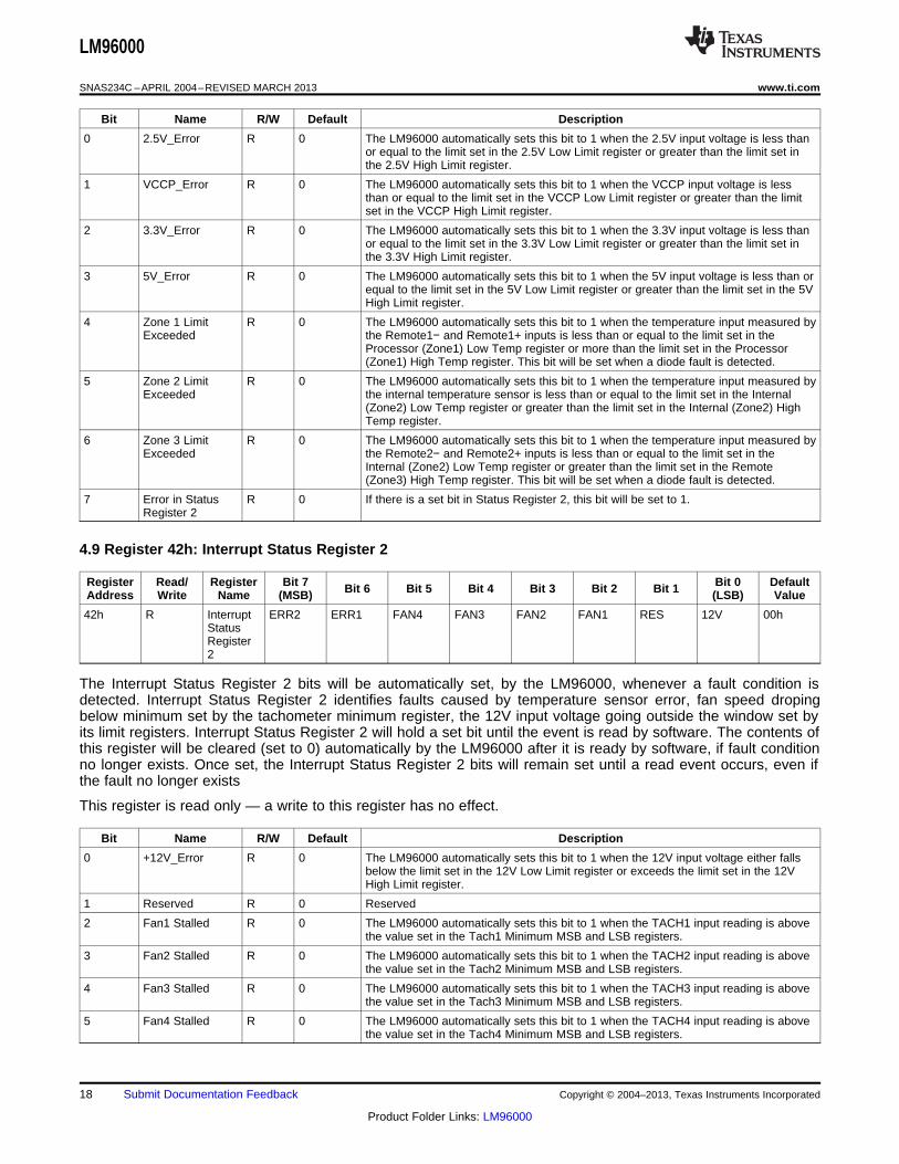
Bit Name R/W Default Description
0 2.5V_Error R 0 The LM96000 automatically sets this bit to 1 when the 2.5V input voltage is less thanor equal to the limit set in the 2.5V Low Limit register or greater than the limit set inthe 2.5V High Limit register.
1 VCCP_Error R 0 The LM96000 automatically sets this bit to 1 when the VCCP input voltage is lessthan or equal to the limit set in the VCCP Low Limit register or greater than the limitset in the VCCP High Limit register.
2 3.3V_Error R 0 The LM96000 automatically sets this bit to 1 when the 3.3V input voltage is less thanor equal to the limit set in the 3.3V Low Limit register or greater than the limit set inthe 3.3V High Limit register.
3 5V_Error R 0 The LM96000 automatically sets this bit to 1 when the 5V input voltage is less than orequal to the limit set in the 5V Low Limit register or greater than the limit set in the 5VHigh Limit register.
4 Zone 1 Limit R 0 The LM96000 automatically sets this bit to 1 when the temperature input measured byExceeded the Remote1− and Remote1+ inputs is less than or equal to the limit set in the
Processor (Zone1) Low Temp register or more than the limit set in the Processor(Zone1) High Temp register. This bit will be set when a diode fault is detected.
5 Zone 2 Limit R 0 The LM96000 automatically sets this bit to 1 when the temperature input measured byExceeded the internal temperature sensor is less than or equal to the limit set in the Internal
(Zone2) Low Temp register or greater than the limit set in the Internal (Zone2) HighTemp register.
6 Zone 3 Limit R 0 The LM96000 automatically sets this bit to 1 when the temperature input measured byExceeded the Remote2− and Remote2+ inputs is less than or equal to the limit set in the
Internal (Zone2) Low Temp register or greater than the limit set in the Remote(Zone3) High Temp register. This bit will be set when a diode fault is detected.
7 Error in Status R 0 If there is a set bit in Status Register 2, this bit will be set to 1.Register 2
4.9 Register 42h: Interrupt Status Register 2
Register Read/ Register Bit 7 Bit 0 DefaultBit 6 Bit 5 Bit 4 Bit 3 Bit 2 Bit 1Address Write Name (MSB) (LSB) Value
42h R Interrupt ERR2 ERR1 FAN4 FAN3 FAN2 FAN1 RES 12V 00hStatusRegister2
The Interrupt Status Register 2 bits will be automatically set, by the LM96000, whenever a fault condition isdetected. Interrupt Status Register 2 identifies faults caused by temperature sensor error, fan speed dropingbelow minimum set by the tachometer minimum register, the 12V input voltage going outside the window set byits limit registers. Interrupt Status Register 2 will hold a set bit until the event is read by software. The contents ofthis register will be cleared (set to 0) automatically by the LM96000 after it is ready by software, if fault conditionno longer exists. Once set, the Interrupt Status Register 2 bits will remain set until a read event occurs, even ifthe fault no longer exists
This register is read only — a write to this register has no effect.
Bit Name R/W Default Description
0 +12V_Error R 0 The LM96000 automatically sets this bit to 1 when the 12V input voltage either fallsbelow the limit set in the 12V Low Limit register or exceeds the limit set in the 12VHigh Limit register.
1 Reserved R 0 Reserved
2 Fan1 Stalled R 0 The LM96000 automatically sets this bit to 1 when the TACH1 input reading is abovethe value set in the Tach1 Minimum MSB and LSB registers.
3 Fan2 Stalled R 0 The LM96000 automatically sets this bit to 1 when the TACH2 input reading is abovethe value set in the Tach2 Minimum MSB and LSB registers.
4 Fan3 Stalled R 0 The LM96000 automatically sets this bit to 1 when the TACH3 input reading is abovethe value set in the Tach3 Minimum MSB and LSB registers.
5 Fan4 Stalled R 0 The LM96000 automatically sets this bit to 1 when the TACH4 input reading is abovethe value set in the Tach4 Minimum MSB and LSB registers.
18 Submit Documentation Feedback Copyright © 2004–2013, Texas Instruments Incorporated
Product Folder Links: LM96000
LM96000
www.ti.com SNAS234C –APRIL 2004–REVISED MARCH 2013
Bit Name R/W Default Description
6 Remote Diode 1 R 0 The LM96000 automatically sets this bit to 1 when there is either a short or openFault circuit fault on the Remote1+ or Remote1− thermal diode input pins. A diode fault will
also set bit 4, Diode 1 Zone Limit bit, of Interrupt Status Register 1.
7 Remote Diode 2 R 0 The LM96000 automatically sets this bit to 1 when there is either a short or openFault circuit fault on the Remote2+ or Remote2− thermal diode input pins. A diode fault will
also set bit 6, Diode 2 Zone Limit bit, of Interrupt Status Register 1.
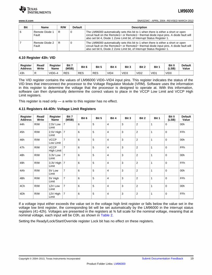
4.10 Register 43h: VID
Register Read/ Register Bit 7 Bit 0 DefaultBit 6 Bit 5 Bit 4 Bit 3 Bit 2 Bit 1Address Write Name (MSB) (LSB) Value
43h R VID0–4 RES RES RES VID4 VID3 VID2 VID1 VID0
The VID register contains the values of LM96000 VID0–VID4 input pins. This register indicates the status of theVID lines that interconnect the processor to the Voltage Regulator Module (VRM). Software uses the informationin this register to determine the voltage that the processor is designed to operate at. With this information,software can then dynamically determine the correct values to place in the VCCP Low Limit and VCCP HighLimit registers.
This register is read only — a write to this register has no effect.
4.11 Registers 44-4Dh: Voltage Limit Registers
Register Read/ Register Bit 7 Bit 0 DefaultBit 6 Bit 5 Bit 4 Bit 3 Bit 2 Bit 1Address Write Name (MSB) (LSB) Value
44h R/W 2.5V Low 7 6 5 4 3 2 1 0 00hLimit
45h R/W 2.5V High 7 6 5 4 3 2 1 0 FFhLimit
46h R/W VCCP 7 6 5 4 3 2 1 0 00hLow Limit
47h R/W VCCP 7 6 5 4 3 2 1 0 FFhHigh Limit
48h R/W 3.3V Low 7 6 5 4 3 2 1 0 00hLimit
49h R/W 3.3V High 7 6 5 4 3 2 1 0 FFhLimit
4Ah R/W 5V Low 7 6 5 4 3 2 1 0 00hLimit
4Bh R/W 5V High 7 6 5 4 3 2 1 0 FFhLimit
4Ch R/W 12V Low 7 6 5 4 3 2 1 0 00hLimit
4Dh R/W 12V High 7 6 5 4 3 2 1 0 FFhLimit
If a voltage input either exceeds the value set in the voltage high limit register or falls below the value set in thevoltage low limit register, the corresponding bit will be set automatically by the LM96000 in the interrupt statusregisters (41-42h). Voltages are presented in the registers at ¾ full scale for the nominal voltage, meaning that atnominal voltage, each input will be C0h, as shown in Table 2.
Setting the Ready/Lock/Start/Override register Lock bit has no effect on these registers.
Copyright © 2004–2013, Texas Instruments Incorporated Submit Documentation Feedback 19
Product Folder Links: LM96000
LM96000
SNAS234C –APRIL 2004–REVISED MARCH 2013 www.ti.com
Table 2. Voltage Limits vs Register Setting
Register Reading Register ReadingRegister SettingNominal Maximum at Minimum atInput atVoltage Voltage Maximum Voltage MinimumNominal Voltage Voltage Voltage
2.5V 2.5V C0h 3.32V FFh 0V 00h
VCCP 2.25V C0h 3.00V FFh 0V 00h
3.3V 3.3V C0h 4.38V FFh 3.0V AFh
5V 5.0V C0h 6.64V FFh 0V 00h
12V 12.0V C0h 16.00V FFh 0V 00h
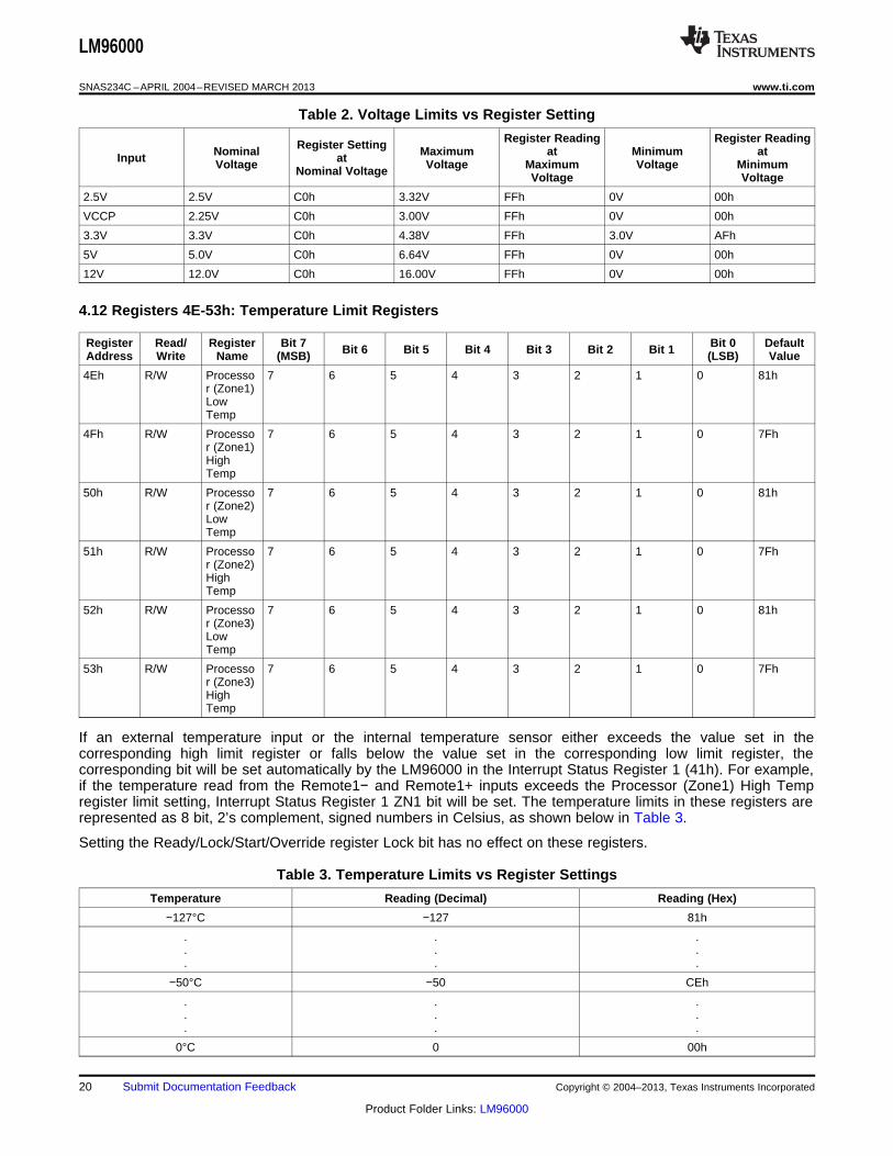
4.12 Registers 4E-53h: Temperature Limit Registers
Register Read/ Register Bit 7 Bit 0 DefaultBit 6 Bit 5 Bit 4 Bit 3 Bit 2 Bit 1Address Write Name (MSB) (LSB) Value
4Eh R/W Processo 7 6 5 4 3 2 1 0 81hr (Zone1)LowTemp
4Fh R/W Processo 7 6 5 4 3 2 1 0 7Fhr (Zone1)HighTemp
50h R/W Processo 7 6 5 4 3 2 1 0 81hr (Zone2)LowTemp
51h R/W Processo 7 6 5 4 3 2 1 0 7Fhr (Zone2)HighTemp
52h R/W Processo 7 6 5 4 3 2 1 0 81hr (Zone3)LowTemp
53h R/W Processo 7 6 5 4 3 2 1 0 7Fhr (Zone3)HighTemp
If an external temperature input or the internal temperature sensor either exceeds the value set in thecorresponding high limit register or falls below the value set in the corresponding low limit register, thecorresponding bit will be set automatically by the LM96000 in the Interrupt Status Register 1 (41h). For example,if the temperature read from the Remote1− and Remote1+ inputs exceeds the Processor (Zone1) High Tempregister limit setting, Interrupt Status Register 1 ZN1 bit will be set. The temperature limits in these registers arerepresented as 8 bit, 2’s complement, signed numbers in Celsius, as shown below in Table 3.
Setting the Ready/Lock/Start/Override register Lock bit has no effect on these registers.
Table 3. Temperature Limits vs Register Settings
Temperature Reading (Decimal) Reading (Hex)
−127°C −127 81h
. . .
. . .
. . .
−50°C −50 CEh
. . .
. . .
. . .
0°C 0 00h
20 Submit Documentation Feedback Copyright © 2004–2013, Texas Instruments Incorporated
Product Folder Links: LM96000
LM96000
www.ti.com SNAS234C –APRIL 2004–REVISED MARCH 2013
Table 3. Temperature Limits vs Register Settings (continued)
Temperature Reading (Decimal) Reading (Hex)
. . .
. . .
. . .
50°C 50 32h
. . .
. . .
. . .
127°C 127 7Fh
4.13 Registers 54-5Bh: Fan Tachometer Low Limit
Register Read/ Register Bit 7 Bit 0 DefaultBit 6 Bit 5 Bit 4 Bit 3 Bit 2 Bit 1Address Write Name (MSB) (LSB) Value
54h R/W Tach1 7 6 5 4 3 2 1 0 FFh55h R/W Minimum 15 14 13 12 11 10 9 8 FFh
LSBTach1MinimumMSB
56h R/W Tach2 7 6 5 4 3 2 1 0 FFh57h R/W Minimum 15 14 13 12 11 10 9 8 FFh
LSBTach2MinimumMSB
58h R/W Tach3 7 6 5 4 3 2 1 0 FFh59h R/W Minimum 15 14 13 12 11 10 9 8 FFh
LSBTach3MinimumMSB
5Ah R/W Tach4 7 6 5 4 3 2 1 0 FFh5Bh R/W Minimum 15 14 13 12 11 10 9 8 FFh
LSBTach4MinimumMSB
The Fan Tachometer Low Limit registers indicate the tachometer reading under which the corresponding bit willbe set in the Interrupt Status Register 2 register. In Auto Fan Control mode, the fan can run at low speeds, socare should be taken in software to ensure that the limit is high enough not to cause sporadic alerts. The fantachometer will not cause a bit to be set in Interrupt Status Register 2 if the current value in Current PWM Dutyregisters is 00h or if the fan 1 disabled via the Fan Configuration Register. Interrupts will never be generated fora fan if its minimum is set to FF FFh.
Given the insignificance of Bit 0 and Bit 1, these bits could be programmed to remember which fan is which, asfollows.
Fan Bit 1 Bit 0
CPU 0 0
Memory 0 1
Chassis Front 1 0
Chassis Rear 1 1
Copyright © 2004–2013, Texas Instruments Incorporated Submit Documentation Feedback 21
Product Folder Links: LM96000
LM96000
SNAS234C –APRIL 2004–REVISED MARCH 2013 www.ti.com
Setting the Ready/Lock/Start/Override register Lock bit has no effect these registers.
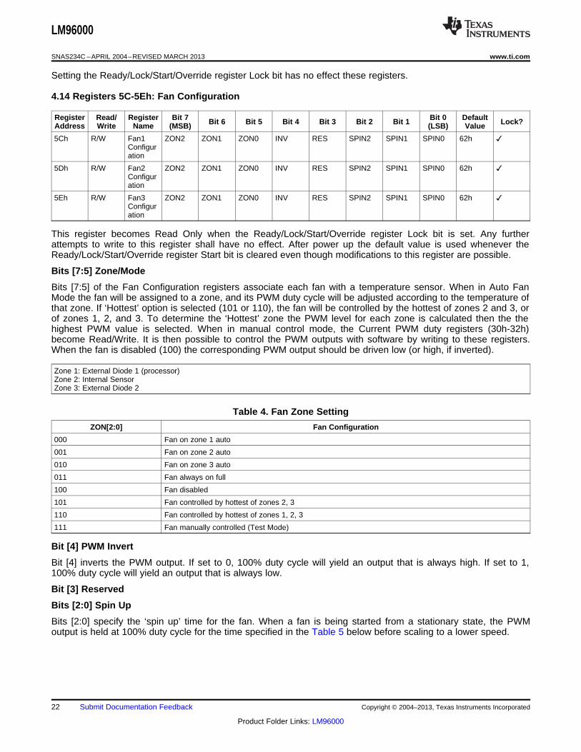
4.14 Registers 5C-5Eh: Fan Configuration
Register Read/ Register Bit 7 Bit 0 DefaultBit 6 Bit 5 Bit 4 Bit 3 Bit 2 Bit 1 Lock?Address Write Name (MSB) (LSB) Value
5Ch R/W Fan1 ZON2 ZON1 ZON0 INV RES SPIN2 SPIN1 SPIN0 62h Configuration
5Dh R/W Fan2 ZON2 ZON1 ZON0 INV RES SPIN2 SPIN1 SPIN0 62h Configuration
5Eh R/W Fan3 ZON2 ZON1 ZON0 INV RES SPIN2 SPIN1 SPIN0 62h Configuration
This register becomes Read Only when the Ready/Lock/Start/Override register Lock bit is set. Any furtherattempts to write to this register shall have no effect. After power up the default value is used whenever theReady/Lock/Start/Override register Start bit is cleared even though modifications to this register are possible.
Bits [7:5] Zone/Mode
Bits [7:5] of the Fan Configuration registers associate each fan with a temperature sensor. When in Auto FanMode the fan will be assigned to a zone, and its PWM duty cycle will be adjusted according to the temperature ofthat zone. If ‘Hottest’ option is selected (101 or 110), the fan will be controlled by the hottest of zones 2 and 3, orof zones 1, 2, and 3. To determine the ‘Hottest’ zone the PWM level for each zone is calculated then the thehighest PWM value is selected. When in manual control mode, the Current PWM duty registers (30h-32h)become Read/Write. It is then possible to control the PWM outputs with software by writing to these registers.When the fan is disabled (100) the corresponding PWM output should be driven low (or high, if inverted).
Zone 1: External Diode 1 (processor)Zone 2: Internal SensorZone 3: External Diode 2
Table 4. Fan Zone Setting
ZON[2:0] Fan Configuration
000 Fan on zone 1 auto
001 Fan on zone 2 auto
010 Fan on zone 3 auto
011 Fan always on full
100 Fan disabled
101 Fan controlled by hottest of zones 2, 3
110 Fan controlled by hottest of zones 1, 2, 3
111 Fan manually controlled (Test Mode)
Bit [4] PWM Invert
Bit [4] inverts the PWM output. If set to 0, 100% duty cycle will yield an output that is always high. If set to 1,100% duty cycle will yield an output that is always low.
Bit [3] Reserved
Bits [2:0] Spin Up
Bits [2:0] specify the ‘spin up’ time for the fan. When a fan is being started from a stationary state, the PWMoutput is held at 100% duty cycle for the time specified in the Table 5 below before scaling to a lower speed.
22 Submit Documentation Feedback Copyright © 2004–2013, Texas Instruments Incorporated
Product Folder Links: LM96000
Zone nMin PWM
or
OFF
PWM duty cycle
linearly increasing as
temperature increases
PWM duty cycle linearly
deacreasing as
temperature decreases
PWM duty cycle linearly
decreasing as
temperature decreases
All Zones
100% PWM
Zone n
100% PWM
Zone n PWM set to
Min FanSpeed (64h-
66h)
Zone n PWM set to
Min FanSpeed (64h-
66h)
Fan Temp Limit - HysteresisHysteresis is 0oC-15oC (6Dh-6Eh)
Fan Temp Limit
(67h-69h)
Fan Temp Limit +Range
Range is 2oC to 80oC (5Fh-61h)Absolute Limit
(6Ah-6Ch)
TemperatureCold Hot
LM96000
www.ti.com SNAS234C –APRIL 2004–REVISED MARCH 2013
Table 5. Fan Spin-Up Register
SPIN[2:0] Spin Up Time
000 0 sec
001 100 ms
010 250 ms
011 400 ms
100 700 ms
101 1000 ms
110 2000 ms
111 4000 ms
4.15 Registers 5F-61h: Auto Fan Speed Range, PWM Frequency
Register Read/ Register Bit 7 Bit 0 DefaultBit 6 Bit 5 Bit 4 Bit 3 Bit 2 Bit 1 Lock?Address Write Name (MSB) (LSB) Value
5Fh R/W Zone1 RAN3 RAN2 RAN1 RAN0 HLFRQ FRQ2 FRQ1 FRQ0 C4h Range/Fan1Frequency
60h R/W Zone2 RAN3 RAN2 RAN1 RAN0 HLFRQ FRQ2 FRQ1 FRQ0 C4h Range/Fan2Frequency
61h R/W Zone3 RAN3 RAN2 RAN1 RAN0 HLFRQ FRQ2 FRQ1 FRQ0 C4h Range/Fan3Frequency
In Auto Fan Mode, when the temperature for a zone is above the Temperature Limit (Registers 67-69h) andbelow its Absolute Temperature Limit (Registers 6A-6Ch), the speed of a fan assigned to that zone is determinedas follows.
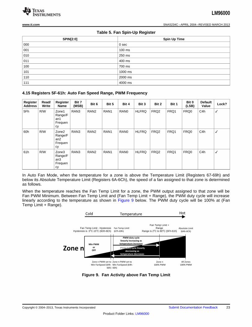
When the temperature reaches the Fan Temp Limit for a zone, the PWM output assigned to that zone will beFan PWM Minimum. Between Fan Temp Limit and (Fan Temp Limit + Range), the PWM duty cycle will increaselinearly according to the temperature as shown in Figure 9 below. The PWM duty cycle will be 100% at (FanTemp Limit + Range).
Figure 9. Fan Activity above Fan Temp Limit
Copyright © 2004–2013, Texas Instruments Incorporated Submit Documentation Feedback 23
Product Folder Links: LM96000
LM96000
SNAS234C –APRIL 2004–REVISED MARCH 2013 www.ti.com
Example for PWM1 assigned to Zone 1:• – Zone 1 Fan Temp Limit (Register 67h) is set to 50°C (32h).• – Range (Register 5Fh) is set to 8°C (6xh).• – Fan 1 PWM Minimum (Register 64h) is set to 50% (32h).
In this case, the PWM1 duty cycle will be 50% at 50°C.
Since (Zone 1 Fan Temp Limit) + (Zone 1 Range) = 50°C + 8°C = 58°C, the fan will run at 100% duty cycle whenthe temperature of the Zone 1 sensor reaches 58°C.
Since the midpoint of the fan control range is 54°C, and the median duty cycle is 75% (Halfway between thePWM Minimum and 100%), PWM1 duty cycle would be 75% at 54°C.
Above (Zone 1 Fan Temp Limit) + (Zone 1 Range), the duty cycle will be 100%.
PWM frequency bits [3:0]
The PWM frequency bits [3:0] determine the PWM frequency for the fan.The LM96000 has high and lowfrequency ranges for the PWM outputs, that are controlled by the HLFRQ bit.
PWM Frequency Selection (Default = 0011 = 30.04 Hz).
Table 6. Register Setting vs PWM Frequency
HLFRQ Freq [2:0] PWM Frequency
0 000 10.01 Hz
0 001 15.02 Hz
0 010 23.14 Hz
0 011 30.04 Hz
0 100 38.16 Hz
0 101 47.06 Hz
0 110 61.38 Hz
0 111 94.12 Hz
1 000 22.5 kHz
1 001 24 kHz
1 010 25.7 kHz
1 011 25.7 kHz
1 100 27.7 kHz
1 101 27.7 kHz
1 110 30 kHz
1 111 30 kHz
Range Selection RAN [3:0]
RAN [3:0] Range (°C)
0000 2
0001 2.5
0010 3.33
0011 4
0100 5
0101 6.67
0110 8
0111 10
1000 13.33
1001 16
1010 20
1011 26.67
24 Submit Documentation Feedback Copyright © 2004–2013, Texas Instruments Incorporated
Product Folder Links: LM96000
35 second Smoothing Filter
OU
TP
UT
100
80
60
40
20
05 10 15 20 25 30 35 400
1.0
0.80.60.40.2
TIME (s)
INP
UT
INPUT
OUTPUT
LM96000
www.ti.com SNAS234C –APRIL 2004–REVISED MARCH 2013
RAN [3:0] Range (°C)
1100 32
1101 40
1110 53.33
1111 80
This register becomes Read Only when the Ready/Lock/Start/Override register Lock bit is set. Any furtherattempts to write to this register shall have no effect. After power up the default value is used whenever theReady/Lock/Start/Override register Start bit is cleared even though modifications to this register are possible.
4.16 Registers 62, 63h: Min/Off, Spike Smoothing
Register Read/ Register Bit 7 Bit 0 DefaultBit 6 Bit 5 Bit 4 Bit 3 Bit 2 Bit 1 Lock?Address Write Name (MSB) (LSB) Value
62h R/W Min/Off, OFF3 OFF2 OFF1 RES ZN1E ZN1-2 ZN1-1 ZN1-0 00h Zone1SpikeSmoothing
63h R/W Zone2, ZN2E ZN2-2 ZN2-1 ZN2-0 ZN3E ZN3-2 ZN3-1 ZN3-0 00h Zone3SpikeSmoothing
The Off/Min Bits [7:5] specify whether the duty cycle will be 0% or Minimum Fan Duty when the measuredtemperature falls below the Temperature LIMIT register setting (see table below). OFF1 applies to fan 1, OFF2applies to fan 2, and OFF3 applies to fan 3.
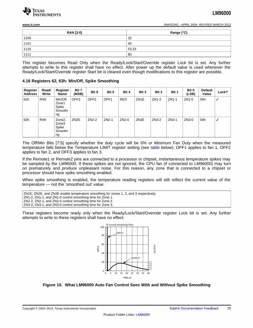
If the Remote1 or Remote2 pins are connected to a processor or chipset, instantaneous temperature spikes maybe sampled by the LM96000. If these spikes are not ignored, the CPU fan (if connected to LM96000) may turnon prematurely and produce unpleasant noise. For this reason, any zone that is connected to a chipset orprocessor should have spike smoothing enabled.
When spike smoothing is enabled, the temperature reading registers will still reflect the current value of thetemperature — not the ‘smoothed out’ value.
ZN1E, ZN2E, and ZN3E enable temperature smoothing for zones 1, 2, and 3 respectively.ZN1-2, ZN1-1, and ZN1-0 control smoothing time for Zone 1.ZN2-2, ZN2-1, and ZN2-0 control smoothing time for Zone 2.ZN3-2, ZN3-1, and ZN3-0 control smoothing time for Zone 3.
These registers become ready only when the Ready/Lock/Start/Override register Lock bit is set. Any furtherattempts to write to these registers shall have no effect.
Figure 10. What LM96000 Auto Fan Control Sees With and Without Spike Smoothing
Copyright © 2004–2013, Texas Instruments Incorporated Submit Documentation Feedback 25
Product Folder Links: LM96000
LM96000
SNAS234C –APRIL 2004–REVISED MARCH 2013 www.ti.com
Table 7. Spike Smoothing
ZN-X[2:0] Spike Smoothed Over
000 35 seconds
001 17.6 seconds
010 11.8 seconds
011 7.0 seconds
100 4.4 seconds
101 3.0 seconds
110 1.6 seconds
111 .8 seconds
Table 8. PWM Output Below Limit Depending on Value of Off/Min
Off/Min PWM Action
0 At 0% duty below LIMIT
1 At Min PWM Duty below LIMIT
4.17 Registers 64-66h: Minimum PWM Duty Cycle
Register Read/ Register Bit 7 Bit 0 DefaultBit 6 Bit 5 Bit 4 Bit 3 Bit 2 Bit 1 Lock?Address Write Name (MSB) (LSB) Value
64h R/W Fan1 7 6 5 4 3 2 1 0 80h PWMMinimum
65h R/W Fan2 7 6 5 4 3 2 1 0 80h PWMMinimum
66h R/W Fan3 7 6 5 4 3 2 1 0 80h PWMMinimum
These registers specify the minimum duty cycle that the PWM will output when the measured temperaturereaches the Temperature LIMIT register setting.
This register becomes Read Only when the Ready/Lock/Start/Override register Lock bit is set. Any furtherattempts to write to this register shall have no effect. After power up the default value is used whenever theReady/Lock/Start/Override register Start bit is cleared even though modifications to this register are possible.
Table 9. PWM Duty vs Register Setting for PWM Low Frequency Range
Current Duty Value (Decimal) Value (Hex)
0% 0 00h
0.3922% 1 01h
. . .
. . .
. . .
25.098% 64 40h
. . .
. . .
. . .
50.196% 128 80h
. . .
. . .
. . .
100% 255 FF
26 Submit Documentation Feedback Copyright © 2004–2013, Texas Instruments Incorporated
Product Folder Links: LM96000
LM96000
www.ti.com SNAS234C –APRIL 2004–REVISED MARCH 2013
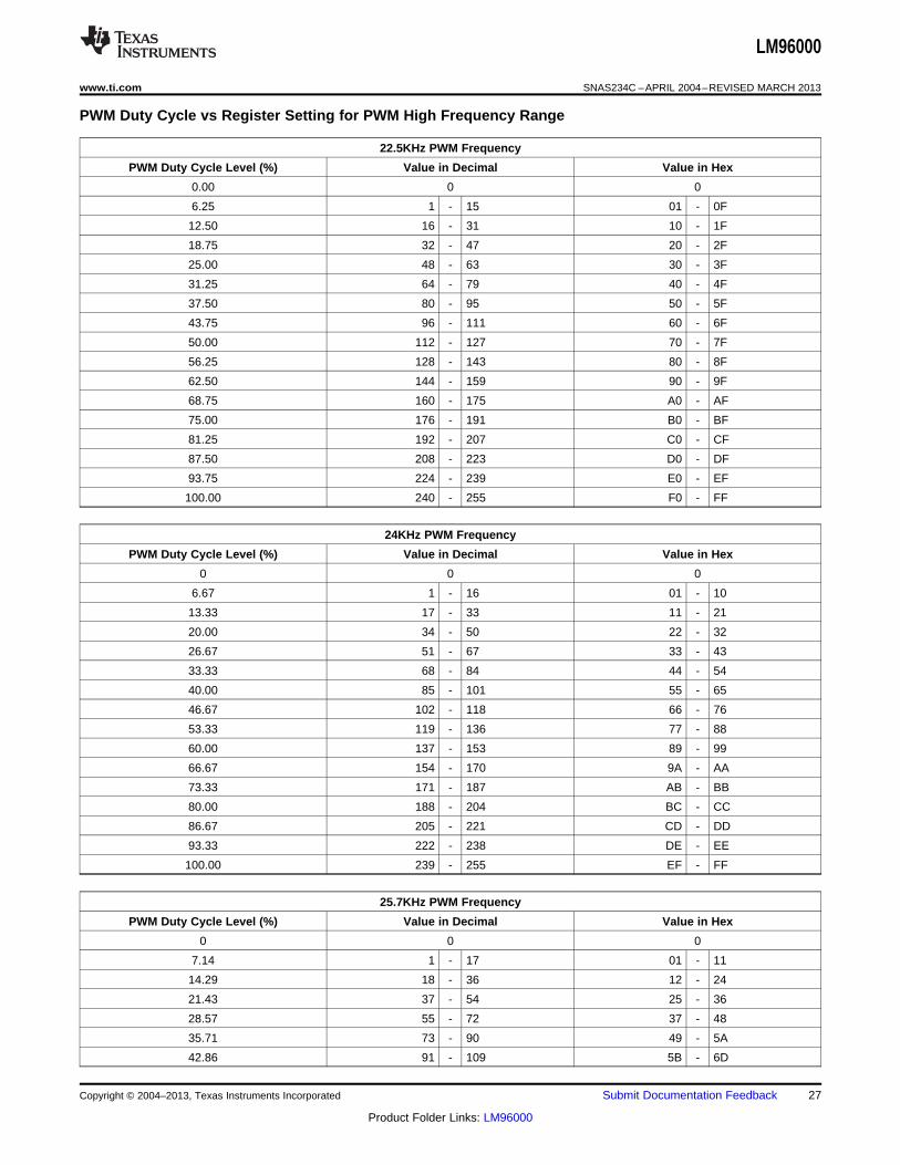
PWM Duty Cycle vs Register Setting for PWM High Frequency Range
22.5KHz PWM Frequency
PWM Duty Cycle Level (%) Value in Decimal Value in Hex
0.00 0 0
6.25 1 - 15 01 - 0F
12.50 16 - 31 10 - 1F
18.75 32 - 47 20 - 2F
25.00 48 - 63 30 - 3F
31.25 64 - 79 40 - 4F
37.50 80 - 95 50 - 5F
43.75 96 - 111 60 - 6F
50.00 112 - 127 70 - 7F
56.25 128 - 143 80 - 8F
62.50 144 - 159 90 - 9F
68.75 160 - 175 A0 - AF
75.00 176 - 191 B0 - BF
81.25 192 - 207 C0 - CF
87.50 208 - 223 D0 - DF
93.75 224 - 239 E0 - EF
100.00 240 - 255 F0 - FF
24KHz PWM Frequency
PWM Duty Cycle Level (%) Value in Decimal Value in Hex
0 0 0
6.67 1 - 16 01 - 10
13.33 17 - 33 11 - 21
20.00 34 - 50 22 - 32
26.67 51 - 67 33 - 43
33.33 68 - 84 44 - 54
40.00 85 - 101 55 - 65
46.67 102 - 118 66 - 76
53.33 119 - 136 77 - 88
60.00 137 - 153 89 - 99
66.67 154 - 170 9A - AA
73.33 171 - 187 AB - BB
80.00 188 - 204 BC - CC
86.67 205 - 221 CD - DD
93.33 222 - 238 DE - EE
100.00 239 - 255 EF - FF
25.7KHz PWM Frequency
PWM Duty Cycle Level (%) Value in Decimal Value in Hex
0 0 0
7.14 1 - 17 01 - 11
14.29 18 - 36 12 - 24
21.43 37 - 54 25 - 36
28.57 55 - 72 37 - 48
35.71 73 - 90 49 - 5A
42.86 91 - 109 5B - 6D
Copyright © 2004–2013, Texas Instruments Incorporated Submit Documentation Feedback 27
Product Folder Links: LM96000
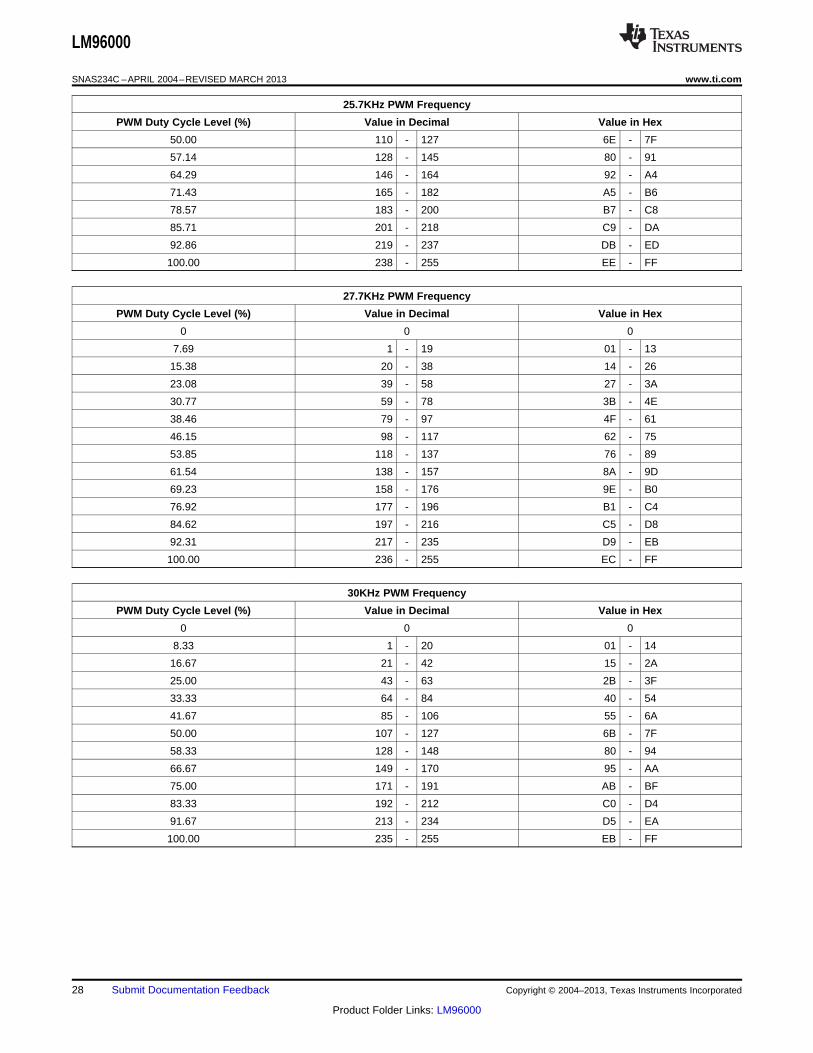
LM96000
SNAS234C –APRIL 2004–REVISED MARCH 2013 www.ti.com
25.7KHz PWM Frequency
PWM Duty Cycle Level (%) Value in Decimal Value in Hex
50.00 110 - 127 6E - 7F
57.14 128 - 145 80 - 91
64.29 146 - 164 92 - A4
71.43 165 - 182 A5 - B6
78.57 183 - 200 B7 - C8
85.71 201 - 218 C9 - DA
92.86 219 - 237 DB - ED
100.00 238 - 255 EE - FF
27.7KHz PWM Frequency
PWM Duty Cycle Level (%) Value in Decimal Value in Hex
0 0 0
7.69 1 - 19 01 - 13
15.38 20 - 38 14 - 26
23.08 39 - 58 27 - 3A
30.77 59 - 78 3B - 4E
38.46 79 - 97 4F - 61
46.15 98 - 117 62 - 75
53.85 118 - 137 76 - 89
61.54 138 - 157 8A - 9D
69.23 158 - 176 9E - B0
76.92 177 - 196 B1 - C4
84.62 197 - 216 C5 - D8
92.31 217 - 235 D9 - EB
100.00 236 - 255 EC - FF
30KHz PWM Frequency
PWM Duty Cycle Level (%) Value in Decimal Value in Hex
0 0 0
8.33 1 - 20 01 - 14
16.67 21 - 42 15 - 2A
25.00 43 - 63 2B - 3F
33.33 64 - 84 40 - 54
41.67 85 - 106 55 - 6A
50.00 107 - 127 6B - 7F
58.33 128 - 148 80 - 94
66.67 149 - 170 95 - AA
75.00 171 - 191 AB - BF
83.33 192 - 212 C0 - D4
91.67 213 - 234 D5 - EA
100.00 235 - 255 EB - FF
28 Submit Documentation Feedback Copyright © 2004–2013, Texas Instruments Incorporated
Product Folder Links: LM96000
LM96000
www.ti.com SNAS234C –APRIL 2004–REVISED MARCH 2013
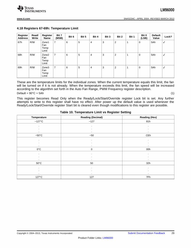
4.18 Registers 67-69h: Temperature Limit
Register Read/ Register Bit 7 Bit 0 DefaultBit 6 Bit 5 Bit 4 Bit 3 Bit 2 Bit 1 Lock?Address Write Name (MSB) (LSB) Value
67h R/W Zone1 7 6 5 4 3 2 1 0 5Ah FanTempLimit
68h R/W Zone2 7 6 5 4 3 2 1 0 5Ah FanTempLimit
69h R/W Zone3 7 6 5 4 3 2 1 0 5Ah FanTempLimit
These are the temperature limits for the individual zones. When the current temperature equals this limit, the fanwill be turned on if it is not already. When the temperature exceeds this limit, the fan speed will be increasedaccording to the algorithm set forth in the Auto Fan Range, PWM Frequency register description.Default = 90°C = 5Ah (1)
This register becomes Read Only when the Ready/Lock/Start/Override register Lock bit is set. Any furtherattempts to write to this register shall have no effect. After power up the default value is used whenever theReady/Lock/Start/Override register Start bit is cleared even though modifications to this register are possible.
Table 10. Temperature Limit vs Register Setting
Temperature Reading (Decimal) Reading (Hex)
−127°C −127 81h
. . .
. . .
. . .
−50°C −50 CEh
. . .
. . .
. . .
0°C 0 00h
. . .
. . .
. . .
50°C 50 32h
. . .
. . .
. . .
127°C 127 7Fh
Copyright © 2004–2013, Texas Instruments Incorporated Submit Documentation Feedback 29
Product Folder Links: LM96000
LM96000
SNAS234C –APRIL 2004–REVISED MARCH 2013 www.ti.com
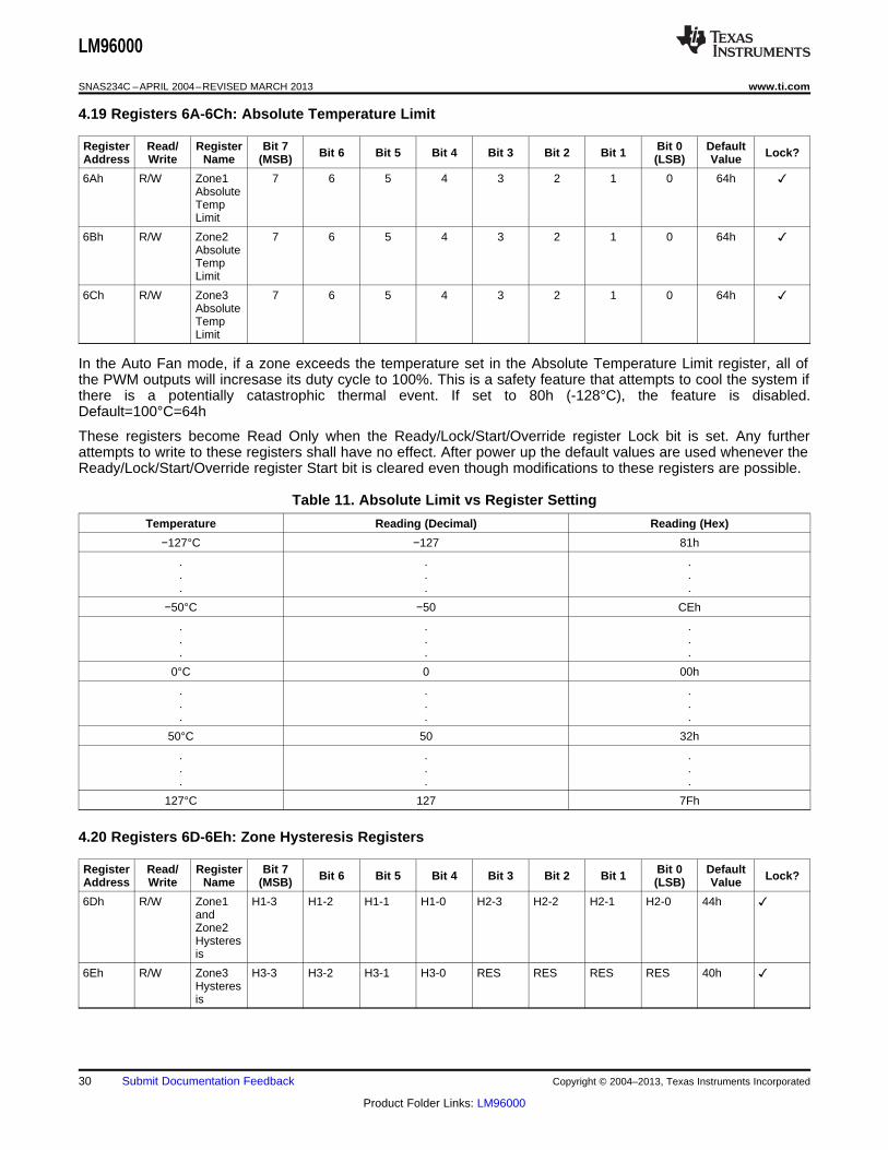
4.19 Registers 6A-6Ch: Absolute Temperature Limit
Register Read/ Register Bit 7 Bit 0 DefaultBit 6 Bit 5 Bit 4 Bit 3 Bit 2 Bit 1 Lock?Address Write Name (MSB) (LSB) Value
6Ah R/W Zone1 7 6 5 4 3 2 1 0 64h AbsoluteTempLimit
6Bh R/W Zone2 7 6 5 4 3 2 1 0 64h AbsoluteTempLimit
6Ch R/W Zone3 7 6 5 4 3 2 1 0 64h AbsoluteTempLimit
In the Auto Fan mode, if a zone exceeds the temperature set in the Absolute Temperature Limit register, all ofthe PWM outputs will incresase its duty cycle to 100%. This is a safety feature that attempts to cool the system ifthere is a potentially catastrophic thermal event. If set to 80h (-128°C), the feature is disabled.Default=100°C=64h
These registers become Read Only when the Ready/Lock/Start/Override register Lock bit is set. Any furtherattempts to write to these registers shall have no effect. After power up the default values are used whenever theReady/Lock/Start/Override register Start bit is cleared even though modifications to these registers are possible.
Table 11. Absolute Limit vs Register Setting
Temperature Reading (Decimal) Reading (Hex)
−127°C −127 81h
. . .
. . .
. . .
−50°C −50 CEh
. . .
. . .
. . .
0°C 0 00h
. . .
. . .
. . .
50°C 50 32h
. . .
. . .
. . .
127°C 127 7Fh
4.20 Registers 6D-6Eh: Zone Hysteresis Registers
Register Read/ Register Bit 7 Bit 0 DefaultBit 6 Bit 5 Bit 4 Bit 3 Bit 2 Bit 1 Lock?Address Write Name (MSB) (LSB) Value
6Dh R/W Zone1 H1-3 H1-2 H1-1 H1-0 H2-3 H2-2 H2-1 H2-0 44h andZone2Hysteresis
6Eh R/W Zone3 H3-3 H3-2 H3-1 H3-0 RES RES RES RES 40h Hysteresis
30 Submit Documentation Feedback Copyright © 2004–2013, Texas Instruments Incorporated
Product Folder Links: LM96000
LM96000
www.ti.com SNAS234C –APRIL 2004–REVISED MARCH 2013
If the temperature is above Fan Temp Limit, then drops below Fan Temp Limit, the following will occur:• – The fan will remain on, at Fan PWM Minimum, until the temperature goes a certain amount below Fan
Temp Limit.• – The Hysteresis registers control this amount. See below table for details.
These registers become Read Only when the Ready/Lock/Start/Override register Lock bit is set. Any furtherattempts to write to thses registers shall have no effect. After power up the default value is used whenever theReady/Lock/Start/Override register Start bit is cleared even though modifications to this register are possible.
Table 12. Hysteresis Settings
Setting HYSTERESIS
0h 0°C
. .
. .
. .
5h 5°C
. .
. .
. .
Fh 15°C
4.21 Register 6Fh: Test Register
Register Read/ Register Bit 7 Bit 0 DefaultBit 6 Bit 5 Bit 4 Bit 3 Bit 2 Bit 1Address Write Name (MSB) (LSB) Value
6Fh R/W Test RES RES RES RES RES RES RES XEN 00hRegister
If the XEN bit is set high, the part will be placed into XOR tree test mode. Clearing the bit (writing a 0 to the XENbit) brings the part out of XOR tree test mode.
This register becomes Read Only when the Ready/Lock/Start/Override register Lock bit is set. Any furtherattempts to write to this registers shall have no effect. After power up the default value is used whenever theReady/Lock/Start/Override register Start bit is cleared even though modifications to this register are possible.
4.22 Registers 70-7Fh: Vendor Specific Registers
These registers are for vendor specific features, including test registers. They will not default to a specific valueon power up.
4.22.1 Register 74h: Tachometer Monitor Mode
Register Read/ Register Bit 7 Bit 0 DefaultBit 6 Bit 5 Bit 4 Bit 3 Bit 2 Bit 1 Lock?Address Write Name (MSb) (LSb) Value
74h R/W Tach RES RES T3/4-1 T3/4-0 T2-1 T2-0 T1-1 T1-0 00hMonitorMode
Each fan TACH input has 4 possible modes of operation when using the low frequency range for the PWMoutputs. Mode 0 is the only mode that is available when using the high frequecy range for the PWM outputs. Themodes for TACH3 and TACH4 share control bits T3/4-[1:0]; TACH2 is controlled by T2-[1:0]; TACH1 is controlledby T1-[1:0]. The result reported in all modes is based on 2 pulses per revolution. In order for modes 2 and 3 tofunction properly it is required that the:• PWM1 output must control the fan that has it's tachometer output connected to the TACH1 LM96000 input.• PWM2 output must control the fan that has it's tachometer output connected to the TACH2 LM96000 input.• PWM3 output must control the fans that have their tachometer outputs connected to the TACH3 or TACH4
LM96000 inputs.
Copyright © 2004–2013, Texas Instruments Incorporated Submit Documentation Feedback 31
Product Folder Links: LM96000
LM96000
SNAS234C –APRIL 2004–REVISED MARCH 2013 www.ti.com
Setting (Tn[1:0]) Mode Function
00 0 Traditional tach input monitor, false readingswhen under minimum detctable RPM
01 1 Traditional tach input monitor, FFFFh readingwhen under minimum detectable RPM
10 2 Most accurate readings, FFFFh readingwhen under minimum detectable RPM
11 3 Least effect on programmed PWM of Fan,FFFFh reading when under minimumdetectable RPM
• Mode 0: This mode uses the conventional method for fan tachometer pulse detection and does not include any circuitry tocompensate for PWM Fan drive. This mode should be used when PWM drive is not used to power the fan. This mode mayreport a false RPM reading when under minimum detectable RPM as shown in the following table.
• Mode 1: This mode uses the conventional method for fan tach detection. The reading will be FFFFh if it is below minimum detectableRPM.
• Mode 2: This mode is optimized for accurate RPM readings and activates circuitry that extends the lower side of the RPM reading asshown in the following table.
• Mode 3: This mode minimizes the effect on the RPM setting and activates circuitry that extends the lower side of the RPM reading asshown in the following table.
PWM Frequency Mode 0 and 1 Minimum RPM Mode 2 and 3 Minimum RPM
10.01 841 210
15.02 1262 315
23.14 1944 420
30.04 2523 420
38.16 3205 420
47.06 3953 420
61.38 5156 420
94.12 7906 420
This register is not effected when the Ready/Lock/Start/Override register Lock bit is set. After power up thedefault value is used whenever the Ready/Lock/Start/Override register Start bit is cleared even thoughmodifications to this register are possible.
4.22.2 Register 75h: Fan Spin-up Mode
Register Read/ Register Bit 7 Bit 0 DefaultBit 6 Bit 5 Bit 4 Bit 3 Bit 2 Bit 1 Lock?Address Write Name (MSB) (LSB) Value
75h R/W Fan RES RES RES RES RES PWM3 PWM2 PWM1 7h Spin-up SU SU SUMode
The PWM SU bit configures the PWM spin-up mode. If PWM SU is cleared the spin-up time will terminate aftertime programmed by the Fan Configuration register has elapsed. When set to a 1, the spin-up time will terminateearly if the TACH reading exceeds the Tach Minimum value or after the time programmed by the FanConfiguration register has elapsed, whichever occurs first.
This register becomes Read Only when the Ready/Lock/Start/Override register Lock bit is set. Any furtherattempts to write to this register shall have no effect. After power up the default value is used whenever theReady/Lock/Start/Override register Start bit is cleared even though modifications to this register are possible.
4.23 Undefined Registers
Any reads to undefined registers will always return 00h. Writes to undefined registers will have no effect and willnot return an error.
32 Submit Documentation Feedback Copyright © 2004–2013, Texas Instruments Incorporated
Product Folder Links: LM96000
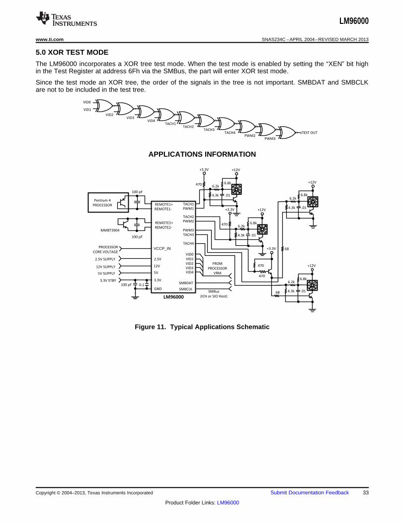
Pentium 4
PROCESSOR
LM96000
REMOTE1+
REMOTE1-
REMOTE2+
REMOTE2-
TACH1
PWM1
VCCP_INVID0
PWM3
PWM2
TACH3
TACH2
TACH4
2.5V
12V
5V
3.3V
GND
VID1
VID2
VID3VID4
SMBDAT
SMBCLK
MMBT3904
100 pF
100 pF
FROM
PROCESSOR
VRM
PROCESSOR
CORE VOLTAGE
2.5V SUPPLY
12V SUPPLY
3.3V STBY
5V SUPPLY
SMBus
(ICH or SIO Host)
100 pF
470
+3.3V
68
0.1
470
+3.3V +12V
470 6.8k
.01
6.2k
4.3k
+3.3V +12V
470 6.8k
.01
6.2k
4.3k
+12V
6.8k
.01
6.2k
4.3k
+12V
6.8k
.01
6.2k
4.3k
68
VID0
VID1
VID2VID3
VID4TACH1
TACH2TACH3
TACH4PWM2
PWM3
xTEST OUT
LM96000
www.ti.com SNAS234C –APRIL 2004–REVISED MARCH 2013
5.0 XOR TEST MODE
The LM96000 incorporates a XOR tree test mode. When the test mode is enabled by setting the “XEN” bit highin the Test Register at address 6Fh via the SMBus, the part will enter XOR test mode.
Since the test mode an XOR tree, the order of the signals in the tree is not important. SMBDAT and SMBCLKare not to be included in the test tree.
APPLICATIONS INFORMATION
Figure 11. Typical Applications Schematic
Copyright © 2004–2013, Texas Instruments Incorporated Submit Documentation Feedback 33
Product Folder Links: LM96000
LM96000
SNAS234C –APRIL 2004–REVISED MARCH 2013 www.ti.com
REVISION HISTORY
Changes from Revision B (March 2013) to Revision C Page
• Changed layout of National Data Sheet to TI format .......................................................................................................... 33
34 Submit Documentation Feedback Copyright © 2004–2013, Texas Instruments Incorporated
Product Folder Links: LM96000
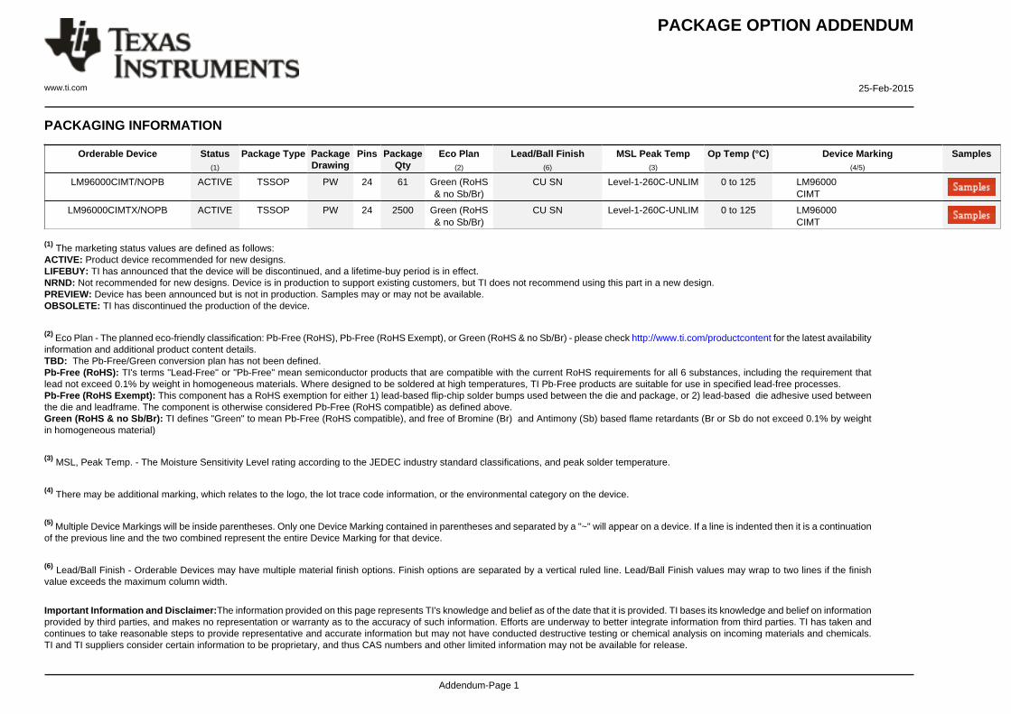
PACKAGE OPTION ADDENDUM
www.ti.com 25-Feb-2015
Addendum-Page 1
PACKAGING INFORMATION
Orderable Device Status(1)
Package Type PackageDrawing
Pins PackageQty
Eco Plan(2)
Lead/Ball Finish(6)
MSL Peak Temp(3)
Op Temp (°C) Device Marking(4/5)
Samples
LM96000CIMT/NOPB ACTIVE TSSOP PW 24 61 Green (RoHS& no Sb/Br)
CU SN Level-1-260C-UNLIM 0 to 125 LM96000CIMT
LM96000CIMTX/NOPB ACTIVE TSSOP PW 24 2500 Green (RoHS& no Sb/Br)
CU SN Level-1-260C-UNLIM 0 to 125 LM96000CIMT
(1) The marketing status values are defined as follows:ACTIVE: Product device recommended for new designs.LIFEBUY: TI has announced that the device will be discontinued, and a lifetime-buy period is in effect.NRND: Not recommended for new designs. Device is in production to support existing customers, but TI does not recommend using this part in a new design.PREVIEW: Device has been announced but is not in production. Samples may or may not be available.OBSOLETE: TI has discontinued the production of the device.
(2) Eco Plan - The planned eco-friendly classification: Pb-Free (RoHS), Pb-Free (RoHS Exempt), or Green (RoHS & no Sb/Br) - please check http://www.ti.com/productcontent for the latest availabilityinformation and additional product content details.TBD: The Pb-Free/Green conversion plan has not been defined.Pb-Free (RoHS): TI's terms "Lead-Free" or "Pb-Free" mean semiconductor products that are compatible with the current RoHS requirements for all 6 substances, including the requirement thatlead not exceed 0.1% by weight in homogeneous materials. Where designed to be soldered at high temperatures, TI Pb-Free products are suitable for use in specified lead-free processes.Pb-Free (RoHS Exempt): This component has a RoHS exemption for either 1) lead-based flip-chip solder bumps used between the die and package, or 2) lead-based die adhesive used betweenthe die and leadframe. The component is otherwise considered Pb-Free (RoHS compatible) as defined above.Green (RoHS & no Sb/Br): TI defines "Green" to mean Pb-Free (RoHS compatible), and free of Bromine (Br) and Antimony (Sb) based flame retardants (Br or Sb do not exceed 0.1% by weightin homogeneous material)
(3) MSL, Peak Temp. - The Moisture Sensitivity Level rating according to the JEDEC industry standard classifications, and peak solder temperature.
(4) There may be additional marking, which relates to the logo, the lot trace code information, or the environmental category on the device.
(5) Multiple Device Markings will be inside parentheses. Only one Device Marking contained in parentheses and separated by a "~" will appear on a device. If a line is indented then it is a continuationof the previous line and the two combined represent the entire Device Marking for that device.
(6) Lead/Ball Finish - Orderable Devices may have multiple material finish options. Finish options are separated by a vertical ruled line. Lead/Ball Finish values may wrap to two lines if the finishvalue exceeds the maximum column width.
Important Information and Disclaimer:The information provided on this page represents TI's knowledge and belief as of the date that it is provided. TI bases its knowledge and belief on informationprovided by third parties, and makes no representation or warranty as to the accuracy of such information. Efforts are underway to better integrate information from third parties. TI has taken andcontinues to take reasonable steps to provide representative and accurate information but may not have conducted destructive testing or chemical analysis on incoming materials and chemicals.TI and TI suppliers consider certain information to be proprietary, and thus CAS numbers and other limited information may not be available for release.
PACKAGE OPTION ADDENDUM
www.ti.com 25-Feb-2015
Addendum-Page 2
In no event shall TI's liability arising out of such information exceed the total purchase price of the TI part(s) at issue in this document sold by TI to Customer on an annual basis.
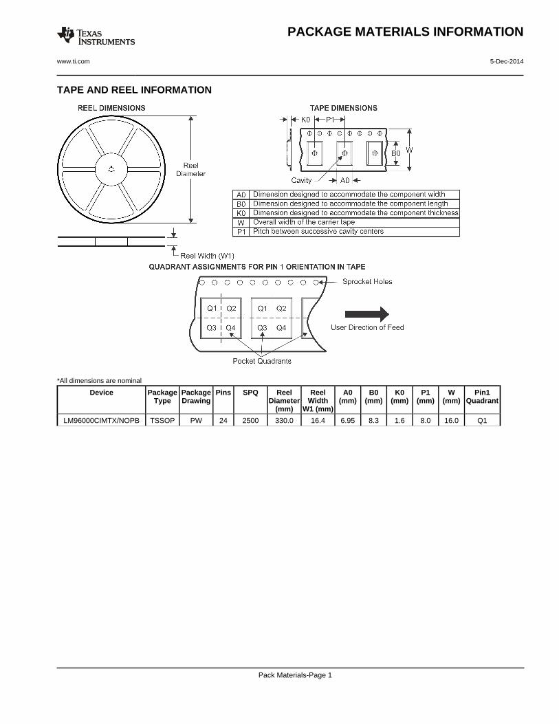
TAPE AND REEL INFORMATION
*All dimensions are nominal
Device PackageType
PackageDrawing
Pins SPQ ReelDiameter
(mm)
ReelWidth
W1 (mm)
A0(mm)
B0(mm)
K0(mm)
P1(mm)
W(mm)
Pin1Quadrant
LM96000CIMTX/NOPB TSSOP PW 24 2500 330.0 16.4 6.95 8.3 1.6 8.0 16.0 Q1
PACKAGE MATERIALS INFORMATION
www.ti.com 5-Dec-2014
Pack Materials-Page 1
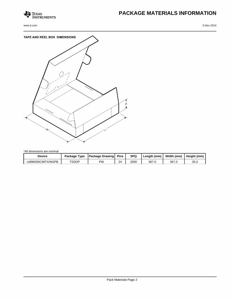
*All dimensions are nominal
Device Package Type Package Drawing Pins SPQ Length (mm) Width (mm) Height (mm)
LM96000CIMTX/NOPB TSSOP PW 24 2500 367.0 367.0 35.0
PACKAGE MATERIALS INFORMATION
www.ti.com 5-Dec-2014
Pack Materials-Page 2
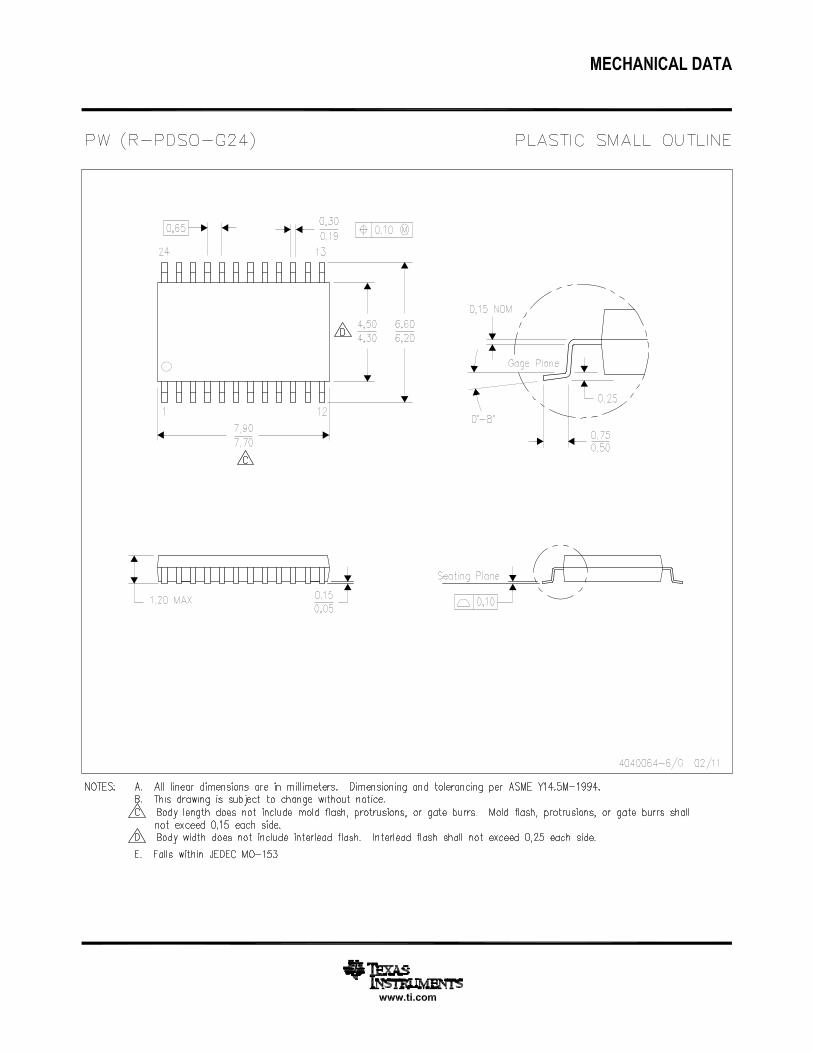
IMPORTANT NOTICE
Texas Instruments Incorporated and its subsidiaries (TI) reserve the right to make corrections, enhancements, improvements and otherchanges to its semiconductor products and services per JESD46, latest issue, and to discontinue any product or service per JESD48, latestissue. Buyers should obtain the latest relevant information before placing orders and should verify that such information is current andcomplete. All semiconductor products (also referred to herein as “components”) are sold subject to TI’s terms and conditions of salesupplied at the time of order acknowledgment.TI warrants performance of its components to the specifications applicable at the time of sale, in accordance with the warranty in TI’s termsand conditions of sale of semiconductor products. Testing and other quality control techniques are used to the extent TI deems necessaryto support this warranty. Except where mandated by applicable law, testing of all parameters of each component is not necessarilyperformed.TI assumes no liability for applications assistance or the design of Buyers’ products. Buyers are responsible for their products andapplications using TI components. To minimize the risks associated with Buyers’ products and applications, Buyers should provideadequate design and operating safeguards.TI does not warrant or represent that any license, either express or implied, is granted under any patent right, copyright, mask work right, orother intellectual property right relating to any combination, machine, or process in which TI components or services are used. Informationpublished by TI regarding third-party products or services does not constitute a license to use such products or services or a warranty orendorsement thereof. Use of such information may require a license from a third party under the patents or other intellectual property of thethird party, or a license from TI under the patents or other intellectual property of TI.Reproduction of significant portions of TI information in TI data books or data sheets is permissible only if reproduction is without alterationand is accompanied by all associated warranties, conditions, limitations, and notices. TI is not responsible or liable for such altereddocumentation. Information of third parties may be subject to additional restrictions.Resale of TI components or services with statements different from or beyond the parameters stated by TI for that component or servicevoids all express and any implied warranties for the associated TI component or service and is an unfair and deceptive business practice.TI is not responsible or liable for any such statements.Buyer acknowledges and agrees that it is solely responsible for compliance with all legal, regulatory and safety-related requirementsconcerning its products, and any use of TI components in its applications, notwithstanding any applications-related information or supportthat may be provided by TI. Buyer represents and agrees that it has all the necessary expertise to create and implement safeguards whichanticipate dangerous consequences of failures, monitor failures and their consequences, lessen the likelihood of failures that might causeharm and take appropriate remedial actions. Buyer will fully indemnify TI and its representatives against any damages arising out of the useof any TI components in safety-critical applications.In some cases, TI components may be promoted specifically to facilitate safety-related applications. With such components, TI’s goal is tohelp enable customers to design and create their own end-product solutions that meet applicable functional safety standards andrequirements. Nonetheless, such components are subject to these terms.No TI components are authorized for use in FDA Class III (or similar life-critical medical equipment) unless authorized officers of the partieshave executed a special agreement specifically governing such use.Only those TI components which TI has specifically designated as military grade or “enhanced plastic” are designed and intended for use inmilitary/aerospace applications or environments. Buyer acknowledges and agrees that any military or aerospace use of TI componentswhich have not been so designated is solely at the Buyer's risk, and that Buyer is solely responsible for compliance with all legal andregulatory requirements in connection with such use.TI has specifically designated certain components as meeting ISO/TS16949 requirements, mainly for automotive use. In any case of use ofnon-designated products, TI will not be responsible for any failure to meet ISO/TS16949.
Products ApplicationsAudio www.ti.com/audio Automotive and Transportation www.ti.com/automotiveAmplifiers amplifier.ti.com Communications and Telecom www.ti.com/communicationsData Converters dataconverter.ti.com Computers and Peripherals www.ti.com/computersDLP® Products www.dlp.com Consumer Electronics www.ti.com/consumer-appsDSP dsp.ti.com Energy and Lighting www.ti.com/energyClocks and Timers www.ti.com/clocks Industrial www.ti.com/industrialInterface interface.ti.com Medical www.ti.com/medicalLogic logic.ti.com Security www.ti.com/securityPower Mgmt power.ti.com Space, Avionics and Defense www.ti.com/space-avionics-defenseMicrocontrollers microcontroller.ti.com Video and Imaging www.ti.com/videoRFID www.ti-rfid.comOMAP Applications Processors www.ti.com/omap TI E2E Community e2e.ti.comWireless Connectivity www.ti.com/wirelessconnectivity
Mailing Address: Texas Instruments, Post Office Box 655303, Dallas, Texas 75265Copyright © 2015, Texas Instruments Incorporated


![ZXSDR BS8800 U240(V4[1].00.30) Hardware Description](https://static.fdocument.org/doc/165x107/5571fcdb4979599169981308/zxsdr-bs8800-u240v410030-hardware-description.jpg)